
Submitted:
15 August 2026
Posted:
18 August 2026
You are already at the latest version
Abstract
This work investigates and compares the weak inversion behavior and drain-induced
barrier lowering (DIBL) of conventional Gate-All- Around (GAA) MOSFETs and the
recently proposed Gate-All-Inside-and-Around (GAIA) devices from room temperature down
to deep cryogenic conditions ( 5 K). A physics-based electrostatic and transport framework
is developed to analyze short-channel effects in the subthreshold regime, where cryogenic
operation significantly modifies carrier statistics, threshold voltage, and subthreshold slope.
Results show that while both architectures benefit from improved electrostatic control
compared to planar devices, GAIA MOSFETs exhibit a systematically reduced DIBL over the
entire temperature range due to an additional insulating barrier that weakens drain-to- channel
electrostatic coupling. At cryogenic temperatures, DIBL is found to be primarily governed by
electrostatic effects rather than thermally activated transport, remaining nearly constant over a
broad temperature range before exhibiting a moderate increase below approximately 30 K. A
compact analytical model is proposed, capturing the combined effects of geometry
and temperature phenomena on DIBL and subthreshold conduction. The results provide new
insights into the role of device architecture in mitigating short-channel effects in cryogenic
CMOS technologies for quantum and ultra-low- power applications.
Keywords:
GAIA MOSFET
; short channel effect
; weak inversion
; subthreshold swing
; DIBL
; cryogenic temperatures
1. Introduction
The continuous downscaling of CMOS technologies has considerably increased the impact of short-channel effects (SCEs), which now constitute one of the main limitations to the electrostatic integrity of nanoscale MOSFETs. Among these effects, drain-induced barrier lowering (DIBL) is particularly critical because it directly affects threshold voltage stability, off-state leakage current and subthreshold operation. As transistor dimensions approach the nanometer scale, maintaining strong electrostatic control of the channel has become one of the major challenges for future CMOS technologies. Consequently, multi-gate device architectures, and in particular Gate-All-Around (GAA) MOSFETs, have emerged as the most promising candidates for ultimate CMOS scaling owing to their superior gate controllability and excellent immunity against short-channel effects [1,2,3,4].
Recently, a new transistor concept, referred to as the Gate-All-Inside-and-Around (GAIA) MOSFET, has been proposed by Balestra and Ghibaudo [5]. Unlike conventional GAA devices, the GAIA architecture introduces an additional insulating cylindrical region inducing two concentric inversion channels, thereby creating a novel electrostatic configuration that simultaneously increases the effective conduction perimeter and improves channel electrostatic confinement. Previous investigations performed at room temperature have demonstrated that this architecture provides higher drive current together with reduced short-channel effects compared with conventional GAA MOSFETs [5]. However, its behavior under cryogenic operating conditions has not yet been investigated.
In parallel with the evolution of CMOS device architectures, cryogenic CMOS electronics has attracted considerable interest during the last decade owing to its key role in emerging applications such as quantum computing, cryogenic sensors, superconducting electronics, and ultra-low-power integrated systems [6,7,8,9,10]. In these applications, CMOS circuits are required to operate over a very wide temperature range extending from room temperature down to liquid-helium temperature, where the physical mechanisms governing carrier transport differ substantially from those encountered under ambient conditions.
It is now well established that cryogenic operation profoundly modifies MOSFET electrical characteristics. Carrier mobility generally increases as phonon scattering is reduced, whereas threshold voltage, subthreshold swing, transconductance efficiency, and leakage currents are strongly affected by incomplete dopant ionization, interface traps, band-tail states, and Fermi-Dirac carrier statistics [6,7,8,9,10,11,12]. Consequently, the development of accurate physical models describing MOSFET behavior at deep cryogenic temperatures has become an essential prerequisite for the design of future Cryo-CMOS integrated circuits.
In the weak inversion regime, the drain current is classically described by diffusion-based transport models developed for MOS transistors [13,14], which predict an ideal subthreshold swing of approximately 60 mV/dec at 300 K and values below 1 mV/dec at liquid-helium temperature. In practice, however, experimental devices systematically deviate from these ideal predictions because several low-temperature physical mechanisms alter the carrier distribution and electrostatic potential within the channel [6,7,8,9,10].
Drain-induced barrier lowering, commonly defined as DIBL=-ΔVth/ΔVd, originates from the electrostatic coupling between the drain and the source-channel potential barrier. Although DIBL is generally considered to be less temperature dependent than thermally activated transport phenomena, cryogenic operation modifies both carrier statistics and charge distribution, which may significantly influence its behavior in the weak inversion regime [11,15,16]. Nevertheless, while threshold voltage, mobility, and subthreshold swing have been extensively investigated in cryogenic MOSFETs, comparatively little attention has been devoted to the systematic study of DIBL in advanced multi-gate architectures operated down to deep cryogenic temperatures.
To the best of our knowledge, no comparative investigation has yet been reported on the weak-inversion operation and drain-induced barrier lowering of GAIA and conventional GAA MOSFETs over the entire temperature range extending from room temperature down to 5 K. Furthermore, the respective roles of electrostatic confinement and cryogenic carrier statistics in determining the DIBL behavior of these architectures remain poorly understood.
In this work, we present a comprehensive numerical investigation of the weak-inversion operation of conventional GAA and novel GAIA MOSFETs using two-dimensional TCAD simulations combined with physics-based analytical modeling. The evolution of the transfer and output characteristics, subthreshold swing, threshold voltage, and drain-induced barrier lowering is analyzed from 300 K down to 5 K for different channel lengths. Particular attention is devoted to identifying the physical mechanisms responsible for the low-temperature evolution of DIBL. The results demonstrate that the superior electrostatic integrity of the GAIA architecture is preserved over the entire cryogenic temperature range. Moreover, they show that the moderate increase in DIBL observed below approximately 30 K originates primarily from the progressive transition between Maxwell-Boltzmann and Fermi-Dirac carrier statistics occurring near the source and drain regions rather than from significant modifications of the electrostatic potential itself. Finally, simple analytical expressions are proposed to accurately describe the temperature and geometrical dependences of the principal weak-inversion parameters, providing compact models suitable for the simulation of future cryogenic CMOS circuits.
2. Structure Description and Simulation Details
As previously reported in [5], the GAIA architecture consists of a core-shell nanowire incorporating an inner oxide/gate structure. Such a device could be fabricated using a sacrificial Si/SiGe core-shell process similar to that employed in Si/SiGe nanowire technologies [17], followed by the deposition of the inner oxide and metal gate using, for example, atomic layer deposition (ALD). The cross-sectional views of the cylindrical GAIA device and its conventional GAA counterpart are schematically illustrated in Figure 1.
TCAD simulations were performed using the finite-element software FlexPDE [18] in cylindrical coordinates on the device structure shown in Figure 2. For the sake of simplicity, the heavily doped source and drain regions were not explicitly included in the simulations. Instead, they were replaced by built-in potential Vbi boundary conditions, as previously proposed in [19], allowing the electrostatic influence of the source and drain junctions to be accurately reproduced while significantly reducing the computational complexity.
Throughout this work, the silicon channel is itself assumed to be non-intentionally doped, i.e., intrinsic, which is representative of the ultrathin silicon channels commonly employed in advanced CMOS technologies. This assumption has no significant influence on the conclusions of the present study and can readily be extended to any non-degenerate channel doping concentration.
To analyze the device operation, the electrostatic potential and carrier transport were obtained by solving self-consistently the Poisson equation (1) and the electron current continuity equation (2) with appropriate boundary conditions corresponding to the applied gate and drain voltages.
(Silicon) (1a)
(Oxide) (1b)
(Silicon) (2)
where V denotes the electrostatic potential, Uc the quasi-Fermi potential, V0 the silicon mid-gap potential, εox and εsi the dielectric permittivities of the oxide and silicon, respectively, n and p the electron and hole concentrations, T the absolute temperature, k (=kb/q=86µV/K) the reduced Boltzmann constant, and µ the electron mobility (see Table 1).
Since the present work focuses exclusively on the weak inversion regime, the effective electron mobility is assumed to remain independent of both the Fermi level and the inversion charge density. This assumption is physically justified because, under non-degenerate Maxwell-Boltzmann statistics, carrier transport in weak inversion is primarily governed by temperature, whereas mobility exhibits only a weak dependence on the inversion charge and on the dominant scattering mechanisms [7,11,12,19].
Under cryogenic operating conditions, however, the carrier concentrations appearing in Eqs. (1)–(3) must be evaluated using Fermi-Dirac statistics in order to correctly account for the possible onset of carrier degeneracy. The electron and hole concentrations are therefore expressed as [20]:
(3a)
(3b)
where Nc ( ) and Nv (( ) denote the effective density of states in the conduction and valence bands of silicon, respectively, QM is the Hänsch quantum correction factor [21,22], FD represents the Fermi-Dirac integral. For numerical implementation, the latter is approximated by the analytical expression proposed in [19,23]
with c ≈ 0.2. (4)
It is worth noting that, in the weak inversion regime u<<0 the Fermi-Dirac integral naturally converges toward its Maxwell-Boltzmann limit, exp(-u), thereby recovering the classical non-degenerate carrier statistics.
The numerical evaluation of the Fermi-Dirac integral at deep cryogenic temperatures requires special care in order to avoid exponential overflow in Eq. (4). To ensure numerical stability, the following truncated expressions were employed:
(5a)
(5b)
(5c)
where H(u) denotes the Heaviside step function.
The material properties and geometrical parameters used throughout the simulations are summarized in Table 1.
After solving the electrostatic and transport equations for a given set of gate voltages Vg and Vg2 and drain voltage Vd, with the source terminal grounded, the drain current was obtained by integrating the electron current density over the silicon channel cross-section. The resulting drain current was then calculated as a function of gate and drain biases for different temperatures and device geometries.
3. Results and Discussion
3.1. Transfer Characteristics in the Linear Operation Region
Figure 3 presents the simulated transfer characteristics, Id(Vg) of GAIA and GAA nMOS devices with a gate length L=15nm, obtained over a wide temperature range from 300 K down to 10 K. As expected, the drain current in the subthreshold regime exhibits a pronounced temperature dependence for both device architectures. This behavior directly results from the progressive improvement of the subthreshold swing as the temperature decreases, leading to a much steeper turn-on characteristic under cryogenic operation.
In contrast, in the strong inversion regime (see Figure 3b), the drain current becomes nearly independent of temperature because the carrier mobility was assumed to remain constant throughout the simulations. Under these conditions, the drain current mainly reflects the increase of the inversion charge with gate voltage, which can be approximated by Qi≈Cox.(Vg-Vth), where Cox denotes the gate oxide capacitance.
It is also worth noting that the GAIA architecture delivers approximately 2.4 times higher drive current than the conventional GAA device, as previously reported in [5]. This improvement originates from the significantly larger effective conduction perimeter provided by the dual-channel geometry of the GAIA structure, which increases the available inversion charge according to the perimeter ratio [2π(tce/2+tox2)+2π(tce/2+tox2+tsi)]/(2πtsi). Consequently, the GAIA architecture simultaneously offers enhanced electrostatic control and higher current drive capability.
Figure 4(a) shows the evolution of the subthreshold swing function, SS=dVg/dlog(Id) as a function of the drain current for several temperatures in the GAIA device (L=15nm). The subthreshold swing is extracted from the nearly constant plateau observed at low drain current (typically between 10-13 and 10-11 A), where transport is entirely governed by diffusion. The extracted values are subsequently plotted as a function of temperature for both GAIA and GAA devices in Figure 4(b). The subthreshold swing decreases almost linearly with temperature over the investigated range, as expected from the diffusion-controlled weak-inversion regime. This indicates that the weak-inversion transport relevant to the SS extraction remains essentially diffusion controlled.
To evaluate the influence of short-channel effects, the subthreshold swing was extracted for gate lengths ranging from 25 nm down to 10 nm for both device architectures, as shown in Figure 5(a). Although the nearly linear dependence of SS on temperature is preserved for all channel lengths, a progressive degradation of the subthreshold swing is observed as the gate length decreases. This degradation reflects the increasing loss of electrostatic control associated with short-channel effects. A clearer picture is obtained by considering the excess subthreshold swing, SS-SSmin, where SSmin=2.3kT represents the ideal thermal limit. The variations of this quantity with gate length are presented in Figure 5(b). Remarkably, the excess subthreshold swing follows an almost perfect power-law dependence on the gate length, SS-SSmin,∝L-3 over the entire investigated temperature range. This behavior is fully consistent with the scaling law previously reported at room temperature for the GAIA architecture [5], demonstrating that the dominant electrostatic mechanisms governing short-channel effects remain essentially unchanged under cryogenic operation.
Furthermore, the GAIA devices consistently exhibit lower values of both SS and (SS-SSmin) than their GAA counterparts. This confirms the superior electrostatic integrity of the GAIA architecture over the whole range of temperatures and channel lengths considered in this study.
Another key parameter reflecting short-channel effects in the linear operating regime is the threshold voltage, Vth, which was extracted using the constant-current criterion (here Id=10-11 A). As shown in Figure 6(a), the threshold voltage increases monotonically as the temperature decreases, in agreement with the well-established behavior of cryogenic MOSFETs [6,7,8,9]. The threshold voltage roll-off, ΔVth=Vth(L)-Vth(25nm), is plotted as a function of gate length for different temperatures in Figure 6(b). The results clearly indicate that threshold voltage degradation is more pronounced in conventional GAA devices than in GAIA devices, further demonstrating the improved electrostatic control provided by the GAIA architecture. Moreover, the threshold voltage roll-off progressively decreases as the temperature is lowered. This behavior is a direct consequence of the reduction of the subthreshold swing under cryogenic operation since the threshold voltage is extracted at a constant drain current within the weak inversion regime.
This point is further illustrated in Figure 7, which presents the temperature dependence of the threshold voltage extracted using different constant-current criteria. It clearly appears that the observed temperature dependence of Vth strongly depends on the selected current level. As the extraction current is increased toward the strong inversion regime, the threshold voltage becomes progressively less sensitive to temperature and would eventually become nearly temperature independent for sufficiently high inversion levels.
The power-law dependences identified in Figure 5 naturally lead to simple analytical expressions for both the subthreshold swing and the associated constant-current threshold voltage, given by Eqs. (8) and (9), respectively.
(with L in nm) (8)
(with L in nm) . (9)
As illustrated in Figure 8, these compact analytical expressions accurately reproduce the simulated variations of both the subthreshold swing and threshold voltage over a broad range of temperatures and gate lengths. Despite their simplicity, these models successfully capture the dominant electrostatic scaling mechanisms and therefore constitute a useful basis for the development of compact cryogenic MOSFET models suitable for circuit-level simulation.
3.2. Output Characteristics in the Non-Linear Region
The output characteristics Id(Vd) were simulated at each temperature by selecting the gate voltage corresponding to the threshold voltage extracted at a constant drain current here of Id=10-11A for Vd=1mV (see Figure 6). This procedure ensures that all devices operate with the same low-field drain conductance, gd0=Id/Vd (here =10-8S), thereby allowing a meaningful comparison of the output characteristics over the entire temperature range. In the weak inversion regime, the drain current progressively saturates when the drain voltage exceeds approximately 3-4.kT, as predicted by the classical Van Overstraeten diffusion model [13]. Consequently, the simulations were carried out by varying the drain voltage from approximately 0.1kT up to 6kT), depending on temperature, in order to accurately describe the transition from the linear regime to current saturation where drain-induced barrier lowering becomes significant.
Typical simulated output characteristics are presented in Figure 9 for several temperatures extending down to deep cryogenic conditions and for different channel lengths. Owing to the identical low-field conductance imposed by the extraction procedure, all curves initially exhibit the same linear behavior at small drain bias. As the drain voltage increases, current saturation progressively develops, becoming more pronounced for longer channel devices, which are less affected by short-channel effects and therefore exhibit reduced DIBL.
The DIBL coefficient was subsequently extracted from the simulated characteristics using Eq. (7) at Vd=6kT. The corresponding results are presented in Figure 10 as functions of both temperature and channel length. It can be observed that the DIBL remains nearly constant over a broad temperature range, before exhibiting a moderate increase of approximately 30–40% below about 30 K, independently of the channel length. This behavior is in good agreement with previous experimental and modeling studies reported for bulk, FDSOI and more recently FinFET technologies, which have also shown a slight enhancement of DIBL under deep cryogenic operation [6,7,26]. Moreover, the dependence of DIBL on channel length follows a power-law behavior, DIBL∝L-2.5, which is remarkably close to the scaling law previously identified for the excess subthreshold swing. This similarity further confirms that both parameters are governed by the same underlying electrostatic mechanisms associated with short-channel effects.
To better understand the physical origin of the observed DIBL increase at very low temperatures, the electrostatic potential V(x) and electron concentration n(x) were extracted along the channel from the numerical simulations for temperatures ranging from 5 K to 100 K. The corresponding profiles are presented in Figure 11. The electrostatic potential exhibits almost identical spatial distributions over the entire temperature range. This behavior is expected since, in weak inversion, the channel contains only a negligible amount of mobile charge, and the electrostatic potential is therefore mainly determined by the solution of the Poisson equation together with the imposed boundary conditions. In contrast, the electron concentration profiles display a pronounced temperature dependence in the vicinity of the source and drain regions. As the temperature decreases, distinct carrier accumulation humps progressively develop close to both contacts, becoming particularly pronounced below approximately 25 K.
The origin of these humps is clarified in Figure 12(a), where the normalized carrier concentration n/Nc is plotted near the source for different temperatures. The results clearly indicate that these localized carrier accumulations appear as soon as the electron concentration approaches approximately three times the effective density of states, n≈3.Nc, which corresponds to the onset of significant carrier degeneracy under the present conditions. This interpretation is further confirmed by Figure 12(b), which compares the complete Fermi-Dirac statistics with its Maxwell-Boltzmann and degenerate (metallic) asymptotic limits. When n<3.Nc, the semiconductor remains non-degenerate and the classical Maxwell-Boltzmann approximation accurately describes the carrier statistics. Under these conditions, the logarithm of the carrier concentration follows the electrostatic potential almost exactly. Conversely, when n>3.Nc, carrier degeneracy progressively develops and the electron concentration becomes much less sensitive to the local electrostatic potential because of the Fermi-Dirac occupation function. This reduced electrostatic sensitivity gives rise to the carrier accumulation humps observed near the source and drain.
The appearance of these degenerate regions effectively reduces the length of the non-degenerate portion of the channel controlling the current transport. In other words, the electrically active weak-inversion channel becomes slightly shorter as the temperature decreases. This effective channel shortening naturally enhances the electrostatic influence of the drain on the source-channel potential barrier, thereby producing the moderate increase in DIBL observed in the present simulations below approximately 30 K. The present simulations therefore indicate that the low-temperature enhancement of DIBL is not primarily caused by modifications of the electrostatic potential itself, which remains almost unchanged, but rather by the temperature-induced transition from Maxwell-Boltzmann to Fermi-Dirac carrier statistics occurring near the highly injected source and drain regions.
Finally, the simulated output characteristics were modeled using the classical Van Overstraeten weak-inversion formulation [13] enriched by the DIBL correction term [24,25], leading to the analytical expression given by Eq. (10).
As illustrated in Figure 13, the proposed analytical model accurately reproduces the complete Id(Vd/kT) characteristics over the entire temperature range investigated and for different channel lengths. Excellent agreement is obtained from room temperature down to deep cryogenic conditions, demonstrating that the model successfully captures both the electrostatic scaling effects and the statistical mechanisms governing weak-inversion transport.
Although only GAIA devices are presented in Figure 13, an equally good agreement was obtained for conventional GAA MOSFETs, confirming the general validity of the proposed compact formulation.
5. Summary and Conclusions
This work has presented a comprehensive numerical investigation of the weak-inversion operation and short-channel behavior of conventional Gate-All-Around (GAA) and recently proposed Gate-All-Inside-and-Around (GAIA) MOSFETs over a wide temperature range extending from room temperature down to deep cryogenic conditions (5 K). By combining two-dimensional TCAD simulations with physics-based analytical modeling, the influence of temperature and device geometry on the electrostatic integrity of both architectures has been systematically analyzed.
The results demonstrate that cryogenic operation considerably improves the subthreshold characteristics of both devices, leading to an almost linear reduction of the subthreshold swing with temperature, in agreement with the classical diffusion theory in the weak-inversion regime. Although short-channel effects become more pronounced as the gate length is reduced, the excess subthreshold swing follows a unique power-law dependence on channel length over the entire investigated temperature range. Furthermore, the GAIA architecture consistently exhibits lower subthreshold swing degradation and reduced threshold-voltage roll-off than the conventional GAA structure, confirming its superior electrostatic control.
The analysis of the output characteristics further reveals that the drain-induced barrier lowering (DIBL) remains nearly temperature independent over most of the investigated temperature range and increases only moderately below approximately 30 K. Numerical simulations show that this behavior cannot be attributed to significant modifications of the electrostatic potential distribution, which remains essentially unchanged with temperature. Instead, the observed DIBL enhancement originates from the progressive transition from non-degenerate Maxwell-Boltzmann statistics to degenerate Fermi-Dirac carrier statistics in the vicinity of the source and drain regions. The resulting carrier accumulation effectively shortens the electrically active weak-inversion channel, thereby increasing the electrostatic coupling between drain and channel.
Simple analytical expressions describing the temperature and geometrical dependences of the subthreshold swing, threshold voltage, DIBL, and weak-inversion output characteristics have also been proposed. Despite their simplicity, these compact formulations accurately reproduce the numerical simulation results over a broad range of operating conditions, making them attractive candidates for the development of compact cryogenic MOSFET models suitable for circuit-level simulation.
Overall, this study demonstrates that the GAIA architecture provides a significant improvement in electrostatic integrity compared with conventional GAA MOSFETs while preserving excellent weak-inversion characteristics over the entire cryogenic temperature range. Beyond the architectural comparison, the present work also provides a clearer physical understanding of the mechanisms governing short-channel effects under deep cryogenic operation, particularly the respective roles of electrostatics and carrier statistics. These results should contribute to the optimization of future CMOS technologies dedicated to cryogenic electronics, quantum computing interfaces, and ultra-low-power integrated circuits.
Author Contributions
G. Ghibaudo: Conceptualization (equal), Formal analysis (equal), Investigation (equal), Methodology (equal), Writing original draft (equal). F. Balestra: Conceptualization (equal), Formal analysis (equal), Investigation (equal), Methodology (equal), Writing original draft (equal).
Funding
Not applicable.
Data Availability Statement
The data presented in this study are available on request from the corresponding author.
Conflicts of Interest
The authors declare no conflicts of interest.
References
- J. P. Colinge, FinFETs and Other Multi-Gate Transistors. New York, NY, USA: Springer, 2008.
- Loubet, N.; et al. Stacked nanosheet gate-all-around transistor to enable scaling beyond FinFET. Proc. IEEE Symp. VLSI Technol., 2017; pp. T230–T231. [Google Scholar] [CrossRef]
- Gundu, K.; Kursun, V. 5-nm gate-all-around transistor technology with 3-D stacked nanosheets. IEEE Trans. Electron Devices 2022, vol. 69(no. 3), 922–929. [Google Scholar] [CrossRef]
- Taur, Y.; Ning, T. H. Fundamentals of Modern VLSI Devices, 2nd ed.; Cambridge Univ. Press: Cambridge, U.K., 2009. [Google Scholar]
- Balestra, F.; Ghibaudo, G. A novel field effect transistor architecture – the GAIA MOSFET. Eng. Res. Express 2026, vol. 8, 095329. [Google Scholar] [CrossRef]
- Gutierrez-D, E. A.; Deen, J.; Claeys, C. Low Temperature Electronics: Physics, Devices, Circuits, and Applications; Academic Press: Cambridge, MA, USA, 2001. [Google Scholar]
- Balestra, F.; Ghibaudo, G. Device and Circuit Cryogenic Operation for Low Temperature Electronics; Springer: New York, NY, USA, 2001. [Google Scholar]
- Homulle, H.; Song, L.; Charbon, E.; Sebastiano, F. The cryogenic temperature behavior of bipolar, MOS, and DTMOS transistors in standard CMOS. IEEE J. Electron Devices Soc. 2018, vol. 6, 263–270. [Google Scholar] [CrossRef]
- Incandela, R. M.; et al. Characterization and compact modeling of nanometer CMOS transistors at deep-cryogenic temperatures. IEEE J. Electron Devices Soc. 2018, vol. 6, 996–1006. [Google Scholar] [CrossRef]
- Beckers; Jazaeri, F.; Enz, C. Inflection phenomenon in cryogenic MOSFET behavior. IEEE Trans. Electron Devices 2020, vol. 67(no. 3), 1357–1360. [Google Scholar] [CrossRef]
- Cassé, M.; Ghibaudo, G. Low temperature characterization and modeling of FDSOI transistors for Cryo CMOS applications. In in Low-Temperature Technologies and Applications; IntechOpen, 2021. [Google Scholar]
- Serra di Santa Maria, F.; et al. Lambert-W function-based parameter extraction for FDSOI MOSFETs down to deep cryogenic temperatures. Solid-State Electron. 2021, vol. 186, 108175. [Google Scholar] [CrossRef]
- Van Overstraeten, R.; Declerck, G.; Muls, P. Theory of the MOS transistor in weak inversion - new method to determine the number of surface states. IEEE Trans. Electron Devices 1975, vol. 22(no. 5), 282–288. [Google Scholar] [CrossRef]
- Enz, C. C.; Krummenacher, F.; Vittoz, E. A. An analytical MOS transistor model valid in all regions of operation and dedicated to low-voltage and low-current applications. Analog Integr. Circuits Signal Process. 1995, vol. 8(no. 1), 83–114. [Google Scholar] [CrossRef]
- Akturk, et al. Compact and distributed modeling of cryogenic bulk MOSFET operation. IEEE Trans. Electron Devices 2010, vol. 57(no. 6), 1334–1342. [Google Scholar] [CrossRef]
- Dhillon, P.; et al. TCAD modeling of cryogenic nMOSFET ON-state current and subthreshold slope. Proc. IEEE Int. Conf. Simul. Semicond. Process. Devices (SISPAD), 2021; pp. 119–122. [Google Scholar] [CrossRef]
- Jiang, Y.; et al. Omega-gate p-MOSFET with nanowirelike SiGe/Si core/shell channel. IEEE Electron Device Lett. 2009, vol. 30(no. 4), 392–394. [Google Scholar] [CrossRef]
- PDE Solutions Inc., FlexPDE finite-element modeling software. Available online: https://www.pdesolutions.com.
- Ghibaudo, G.; Balestra, F. “Numerical simulation of electro-thermal properties in FDSOI MOSFETs down to deep cryogenic temperatures”. J. Electron. Electr. Eng. 2023, 2, 2498. Available online: https://. [CrossRef]
- Blakemore, J. S. Semiconductor Statistics; Dover Publications: Mineola, NY, USA, 1987. [Google Scholar]
- Hänsch, W.; Vogelsang, T.; Kircher, R.; Orlowski, M. Carrier transport near the Si/SiO2 interface of a MOSFET. Solid-State Electron. 1989, vol. 32(no. 10), 839–849. [Google Scholar] [CrossRef]
- Wang, X.; Tang, T.-W. Comparison of three quantum correction models for the charge density in MOS inversion layers. J. Comput. Electron. 2002, vol. 1, 283–288. [Google Scholar] [CrossRef]
- Catapano, E.; Cassé, M.; Gaillard, F.; de Franceschi, S.; Meunier, T.; Vinet, M.; Ghibaudo, G. TCAD simulations of FDSOI devices down to deep cryogenic temperature. Solid-State Electron. 2022, vol. 194, 108319. [Google Scholar] [CrossRef]
- Tsividis, Y.; McAndrew, C. Operation and Modeling of the MOS Transistor, 3rd ed.; Oxford Univ. Press: New York, NY, USA, 2011. [Google Scholar]
- Ghibaudo, G. Critical MOSFETs operation for low voltage/low power ICs: Ideal characteristics, parameter extraction, electrical noise and RTS fluctuations. Microelectron. Eng. 1997, vol. 39, 31–37. [Google Scholar] [CrossRef]
- Han, H.C.; et al. “Cryogenic characterization of 16 nm FinFET technology for quantum computing”. In ESSCIRC 2021-IEEE 47th European Solid State Circuits Conference (ESSCIRC); IEEE, 2021; pp. 71–74. [Google Scholar] [CrossRef]
Figure 1.
Schematic cross section of GAIA and GAA cylindrical structures with relevant thicknesses.
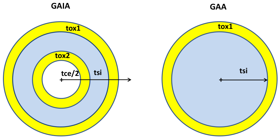
Figure 2.
Schematic of GAIA structure along cylindrical z axis with relevant thicknesses and potential boundary conditions (BC) at gates and source and drain terminals. Short channel conditions are emulated by imposing V=Vbi at source and drain boundaries.
Figure 2.
Schematic of GAIA structure along cylindrical z axis with relevant thicknesses and potential boundary conditions (BC) at gates and source and drain terminals. Short channel conditions are emulated by imposing V=Vbi at source and drain boundaries.
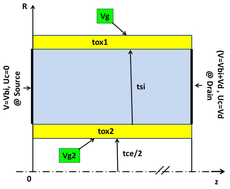
Figure 3.
Id-Vg characteristics in log (a) and linear (b) scales at various temperatures for GAIA (red solid lines) and GAA (blue dashed lines) nMOS devices (L=15nm, Vd=1mV, Vg2=Vg).
Figure 3.
Id-Vg characteristics in log (a) and linear (b) scales at various temperatures for GAIA (red solid lines) and GAA (blue dashed lines) nMOS devices (L=15nm, Vd=1mV, Vg2=Vg).
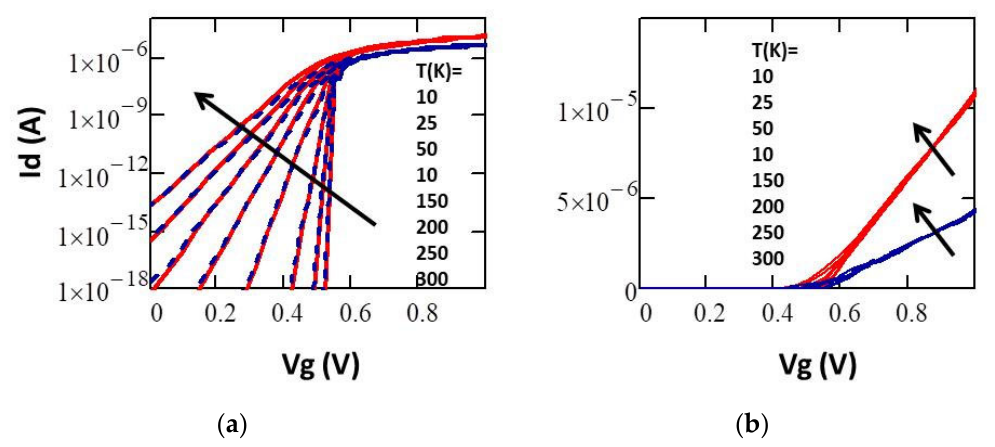
Figure 4.
a) SS=dVg/dlog(Id) versus Id characteristics for various temperatures (GAIA device) and b) variations with temperature of subthreshold swing SS: GAIA (red solid line) and GAA (blue dashed line) (L=15nm, Vd=1mV, Vg2=Vg).
Figure 4.
a) SS=dVg/dlog(Id) versus Id characteristics for various temperatures (GAIA device) and b) variations with temperature of subthreshold swing SS: GAIA (red solid line) and GAA (blue dashed line) (L=15nm, Vd=1mV, Vg2=Vg).
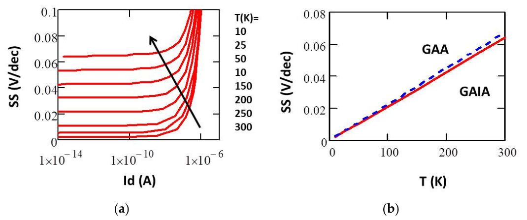
Figure 5.
a) SS versus T for various gate length L and b) (SS-SSmin) versus L for various temperatures T: GAIA=red solid lines, GAA=blue dashed lines (SSmin=2.3kT, Vg2=Vg).
Figure 5.
a) SS versus T for various gate length L and b) (SS-SSmin) versus L for various temperatures T: GAIA=red solid lines, GAA=blue dashed lines (SSmin=2.3kT, Vg2=Vg).
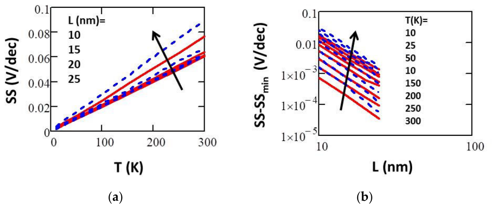
Figure 6.
a) Variations of Vth@Id=10-11A with temperature for various gate lengths and b) variations of ΔVth with gate length for various temperatures: GAIA (red solid lines) and GAA (blue dashed lines) devices (Vd=1mV, Vg2=Vg).
Figure 6.
a) Variations of Vth@Id=10-11A with temperature for various gate lengths and b) variations of ΔVth with gate length for various temperatures: GAIA (red solid lines) and GAA (blue dashed lines) devices (Vd=1mV, Vg2=Vg).
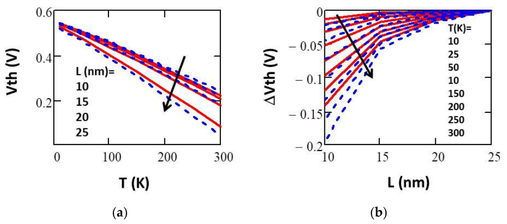
Figure 7.
Variations of Vth with temperature for various constant current measurement levels (GAIA device, L=15nm, Vd=1mV, Vg2=Vg).
Figure 7.
Variations of Vth with temperature for various constant current measurement levels (GAIA device, L=15nm, Vd=1mV, Vg2=Vg).
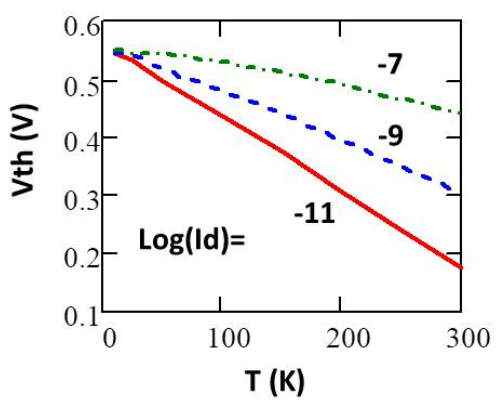
Figure 8.
Simulated (red solid lines) and modeled (blue dashed lines) variations of SS and (SS-SSmin) with T and L or T, and, variations of Vth@Id=10-11A with T and various L for GAIA devices (Vd=1mV, Vg2=Vg).
Figure 8.
Simulated (red solid lines) and modeled (blue dashed lines) variations of SS and (SS-SSmin) with T and L or T, and, variations of Vth@Id=10-11A with T and various L for GAIA devices (Vd=1mV, Vg2=Vg).
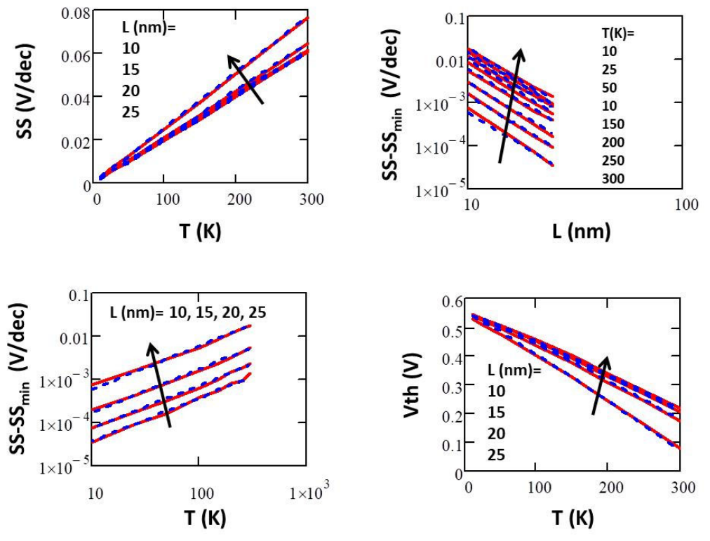
Figure 9.
Id(Vd) output characteristics in log-log scale computed at constant conductance gd0=10-8S i.e., at Vg=Vth@(Id=10-11A & Vd=1mV) for various temperatures and different gate lengths (GAIA devices, Vg2=Vg).
Figure 9.
Id(Vd) output characteristics in log-log scale computed at constant conductance gd0=10-8S i.e., at Vg=Vth@(Id=10-11A & Vd=1mV) for various temperatures and different gate lengths (GAIA devices, Vg2=Vg).
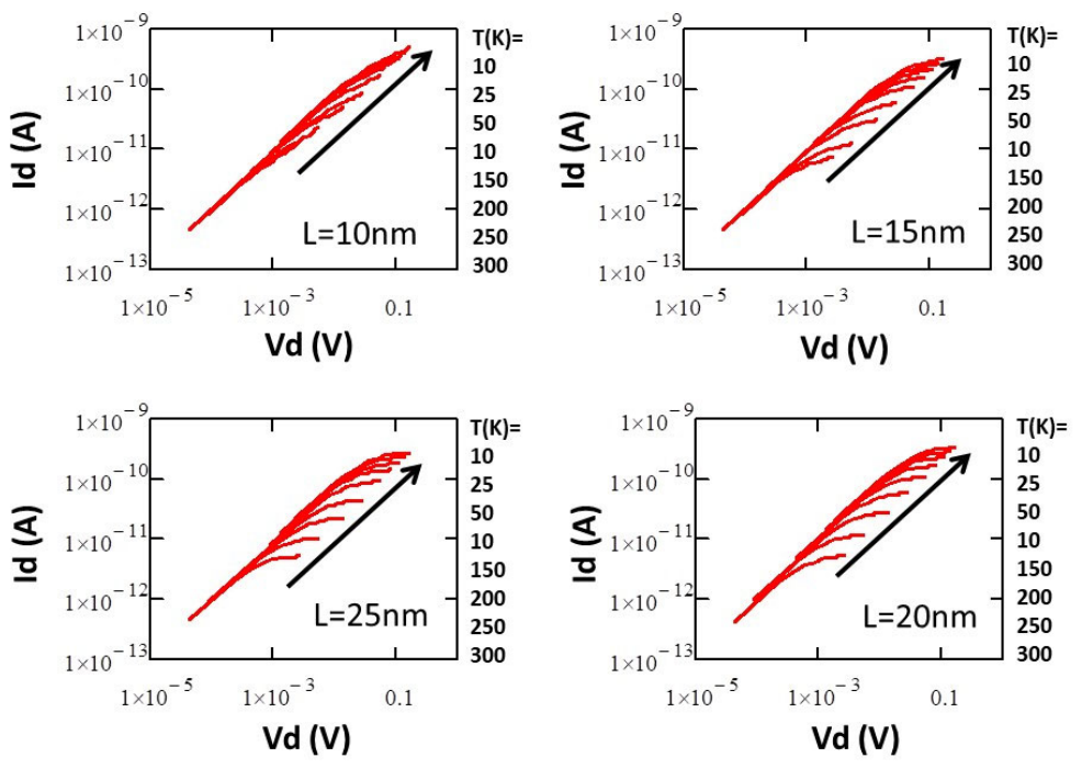
Figure 10.
Variations of DIBL coefficient with temperature (a) and channel length (b) obtained on GAIA MOS devices with constant conductance gd0=10-8S i.e., at Vg=Vth@(Id=10-11A&Vd=1mV, Vg2=Vg).
Figure 10.
Variations of DIBL coefficient with temperature (a) and channel length (b) obtained on GAIA MOS devices with constant conductance gd0=10-8S i.e., at Vg=Vth@(Id=10-11A&Vd=1mV, Vg2=Vg).
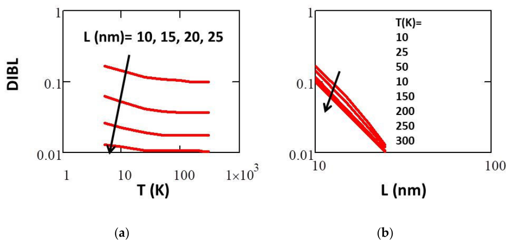
Figure 11.
Electrical potential V(x) and electron density n(x) profiles along the channel between source and drain as obtained on GAIA for various temperatures (Vd=6kT, Vg2=Vg, L=20nm).
Figure 11.
Electrical potential V(x) and electron density n(x) profiles along the channel between source and drain as obtained on GAIA for various temperatures (Vd=6kT, Vg2=Vg, L=20nm).
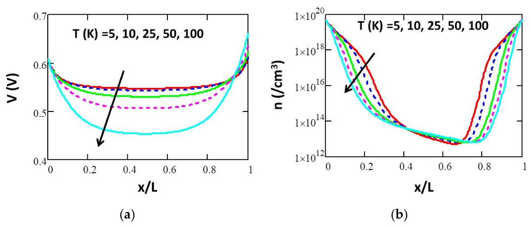
Figure 12.
a) Electron density n(x,T)/Nc(T) profiles near source along the channel as obtained on GAIA for various temperatures. b) Variations of n(x)/Nc as given by full FD statistics (red solid line), MB statistics (blue dashed line) and metallic statistics (green dashed line) for T=5K (Vd=6kT, Vg2=Vg, L=20nm).
Figure 12.
a) Electron density n(x,T)/Nc(T) profiles near source along the channel as obtained on GAIA for various temperatures. b) Variations of n(x)/Nc as given by full FD statistics (red solid line), MB statistics (blue dashed line) and metallic statistics (green dashed line) for T=5K (Vd=6kT, Vg2=Vg, L=20nm).
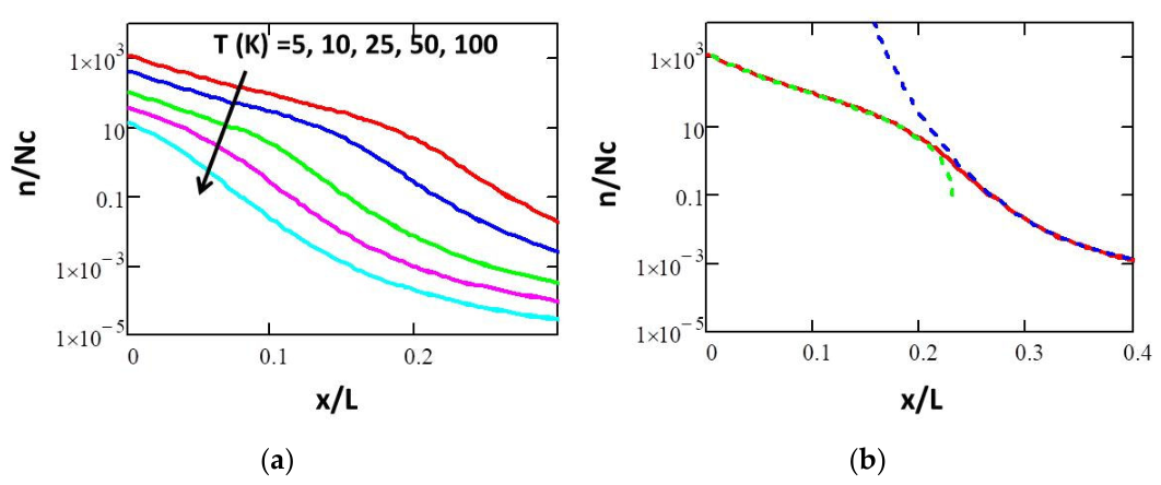
Figure 13.
Simulated (red solid lines) and modeled (blue dashed lines) Id(Vd/kT) output characteristics for L=15nm and L=20nm GAIA MOS devices with constant conductance gd0=10-8S i.e., at Vg=Vth@(Id=10-11A & Vd=1mV, Vg2=Vg).
Figure 13.
Simulated (red solid lines) and modeled (blue dashed lines) Id(Vd/kT) output characteristics for L=15nm and L=20nm GAIA MOS devices with constant conductance gd0=10-8S i.e., at Vg=Vth@(Id=10-11A & Vd=1mV, Vg2=Vg).
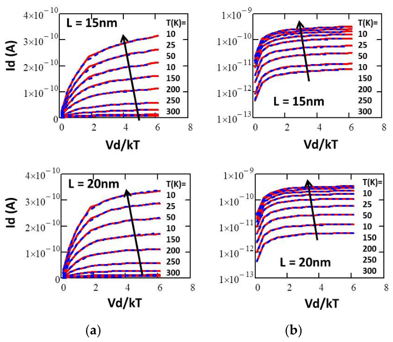

Table 1.
Simulation material and geometrical parameters used in the numerical simulations for GAIA and GAA structures.
Table 1.
Simulation material and geometrical parameters used in the numerical simulations for GAIA and GAA structures.
| Source-Drain doping level | Nd=5x1019 cm-3 |
| Built-in potential at Source-Drain | |
| Si mid-gap potential | V0=0.55 V |
| Si permittivity | εsi=12.ε0 |
| Outer Oxide 1 High K permittivity | εox1=20.ε0 |
| Inner Oxide 2 High K permittivity | εox2=20.ε0 |
| Constant mobility | µ=500 cm2/Vs |
| GAIA nominal thicknesses | tsi=5 nm, tce=5 nm, tox1=1 nm, tox2=1 nm |
| GAA nominal thicknesses | tsi=5 nm, tox1=1 nm |
Disclaimer/Publisher’s Note: The statements, opinions and data contained in all publications are solely those of the individual author(s) and contributor(s) and not of MDPI and/or the editor(s). MDPI and/or the editor(s) disclaim responsibility for any injury to people or property resulting from any ideas, methods, instructions or products referred to in the content. |
© 2026 by the authors. Licensee MDPI, Basel, Switzerland. This article is an open access article distributed under the terms and conditions of the Creative Commons Attribution (CC BY) license (http://creativecommons.org/licenses/by/4.0/).
Copyright: This open access article is published under a Creative Commons CC BY 4.0 license, which permit the free download, distribution, and reuse, provided that the author and preprint are cited in any reuse.