

Submitted:
30 June 2026
Posted:
01 July 2026
You are already at the latest version
Abstract
Surface roughness at the nanometer scale limits the optical performance of reflective components for X-ray and extreme ultraviolet beam shaping. While sub-nanometer roughness can be achieved by polishing planar substrates, it remains challenging for con-tinuous three-dimensional topographies fabricated by grayscale direct-write lithography in polymer resists. In this work, mm-long linear grayscale slopes are introduced as a cali-bration platform to distinguish between form, waviness, and roughness contributions. Process optimization reduces artefacts such as gray-value discretization and stitching, while replication into PMMA combined with the TASTE process enables a reduction of intrinsic roughness below 2 nm. Laser scanning confocal and atomic force microscopy are used as complementary techniques to assess surface quality across spatial scales. The re-sults provide insight into the origin of roughness in novolak-based resists and its evolu-tion through the fabrication chain, highlighting material limitations and paths toward smooth polymer optics.
Keywords:
grayscale lithography
; direct write lithography
; ultra-thick photoresist
; laser scanning confocal microscopy (LSCM)
; atomic force microscopy (AFM)
; polymer replication
; thermally activated selective topography engineering (TASTE)
1. Introduction
Ultra-smooth reflective optics are a key enabling technology for beam shaping and focusing in the X-ray (<10 nm) and extreme ultraviolet (EUV, i.e., 13.5 nm) spectral ranges. At such short wavelengths, as surface height fluctuations translate into phase errors and scattering, nanometer-scale surface irregularities can measurably reduce optical throughput and degrade wavefront quality [1,2,3]. As X-ray and EUV systems move toward higher numerical aperture, tighter tolerances, and larger optical footprints, sub-nanometer to few-nanometer surface roughness is a primary limitation to optical performance [4]. Importantly, optical performance is not determined by a single topology term such as a ”roughness value”: different spatial frequency bands contribute differently to scattering, imaging aberrations, and efficiency loss, making it essential to treat form, waviness, and roughness as distinct quantities (see section 2) [1,5]. Once these components can be identified and systematic errors are mitigated, e.g., via process optimization, single roughness values, e.g., the root mean square (rms) deviation for an area could again become meaningful, not only as an absolute value for comparison of different measurement methods, but also as a relative value for determining whether an improvement can be obtained by fine-tuning fabrication methods involving copying, smoothing and coating processes.
Grayscale direct-write lithography (DWL) using intensity-modulated scanning laser exposure offers an attractive route to fabricate polymer-based three-dimensional (3D) freeform surfaces with CAD-defined topographies [6,7]. In contrast to multi-step etching and polishing workflows, grayscale exposure directly encodes a continuous height map into a single photosensitive resist layer and is compatible with large-area patterning, rapid iteration, and complex shapes. This is particularly valuable when ultra-thick resists (tens to hundreds of micrometers) are required to realize deep optical profiles [8,9]. However, the same discretized dose control that enables grayscale fabrication also introduces deterministic surface artifacts. A finite number of available gray values (GV) quantizes the intended height function and can generate step-induced waviness, while field stitching and scan strategies introduce additional periodic or quasi-periodic height modulations [10]. At the same time, intrinsic resist and process physics—including polymer microstructure, photoactive compound distribution, and dissolution during development—set a roughness floor that can persist through subsequent replication steps [11]. When the roughness gets in the range of nanometers, the sizes of resist molecules and their distribution become non-negligible and nano globular structures become visible [12]. In novolak-based resists used for grayscale DWL, these mechanisms define the intrinsic nanoscale roughness [13,14,15].
A second challenge lies in the metrology of such large features with sub-nm roughness. As already introduced, surface topography of extended free-form structures can be characterized by three distinct components: form, waviness, and roughness [5,16], see Figure 1. In grayscale-fabricated 3D optics, form errors, medium-spatial-frequency waviness, and high-frequency roughness are often not clearly separated, as the analysis relies on filtering procedures that are not unique and can bias the extracted roughness values [16]. Moreover, different instruments probe different spatial bandwidths. Laser scanning confocal microscopy (LSCM) enables rapid, non-contact characterization of millimeter-scale profiles but becomes diffraction- and noise-limited at nanometer roughness levels [17]. In contrast, atomic force microscopy (AFM) provides sub-nanometer vertical resolution but is restricted in scan size and accessibility for deep or high-aspect-ratio structures. A hybrid approach is particularly effective: high-resolution methods such as AFM can be employed for roughness assessment, while techniques like LSCM allow rapid form and artifacts characterization over larger surface areas. The combined approach is therefore required to capture the full spatial spectrum of surface features [18]. Other techniques, such as scattering-based methods, provide integrative measurements over larger surface areas. While efforts have been made to compare roughness across methods and spatial frequencies, the interpretation of results remains strongly dependent on filtering procedures and measurement conditions, complicating direct comparison between techniques [19].
In this work we introduce extended shallow linear grayscale slopes (with ~ 0.5° to 1° inclination) as a controlled calibration platform for ultra-low-roughness grayscale lithography. This enables both (i) the identification and analysis of controlled fabrication of artifacts and (ii) the assessment of the bandwidth limitations inherent to each metrology method [20]. Despite the broad range of possible geometries, we focused on linear slopes with a defined ideal profile and a single-gradient geometry, enabling deviations to be quantified by subtracting a best-fit line (form removal) and then analyzing the residual height signal. These shallow slopes enable the visualization of discretization steps over a wide range of gray values (GVs). Such structures are also directly relevant for applications, as they approximate the shallow gradients found in reflective optical components, including inclined and concave focusing mirrors operating under grazing-incidence conditions over millimeter-scale distances. This geometry allows deterministic contributions, such as gray-value quantization steps, stitching artifacts, and scanner-induced ripples, to be readily identified as waviness, while enabling localized AFM measurements of stochastic roughness in accessible regions. Beyond metrology, linear slopes provide a convenient platform for directly comparing how surface features evolve throughout the complete fabrication chain, from the resist master to replicated polymer structures.
The scope of this paper is: (i) Demonstration of achieving nm-roughness in polymer surfaces manufactured with 3D DWL by eliminating systematic sources of roughness in DWL exposure and development, (ii) use and qualify LSCM and AFM as techniques to assess the quality of measurement, (iii) to establish linear slopes as a practical test structure for separating and quantifying form, waviness, and roughness in ultra-thick grayscale lithography.
2. Materials and Methods
2.1. Grayscale Lithography Fabrication Process
Grayscale lithography was performed using a Heidelberg Instruments DWL 66+ direct laser writer operating at a wavelength of 405 nm. The system employs a scanning laser beam with fast intensity modulation via an acousto-optical modulator, enabling spatially resolved dose control and grayscale exposure. The maximum number of available GV is 1’024 (10-bit gray level dynamic range), and the minimum pixel size is 50 nm. In the DWL 66+ installed at PSI in 2020, that was a big improvement from the DWL 66FS with 128 GVs (4 bit)8 and the µMLA Maskless Aligner with 256 GVs (8 bits) [21]. Current DWL 66+ configurations support substantially higher grayscale resolution to maximum number of addressable 65’536 GVs (16 bit). For shallow slopes, e.g., 10 mm long linear slopes in 100 µm thick resists, and 1’024 GVs, however, this results in 9.7 µm wide steps that are larger than the typical sizes of 0.8 µm or 1.3 µm wide laser beams for the write modes (WM) I (4 mm focal length) and III (10 mm focal length), respectively. This would result in steps that would be separated by horizontal plateaus, while smaller step sizes would be smoothened out by the overlapping laser beam.
The DWL system operates by scanning the laser beam using an acousto-optic deflector over a finite stripe width while the substrate moves in the orthogonal direction. As a result, the exposure is segmented into adjacent stripes with well-defined boundaries in one direction only. Stitching artefacts therefore arise at the interfaces between neighboring stripes, while along the scan direction the exposure is continuous. To reduce the effect of stripe-to-stripe stitching, multi-pass exposure strategies were employed in which the same nominal pattern is distributed over N laterally shifted sub-exposures (called ‘N-over’ N). In this work, CI-over N denotes an advanced strategy offered by the Heidelberg DWL software, of overlapping N sub-fields with a modified intensity distribution along the stripe, that more efficiently smoothens the intensity transition between adjacent sub-fields. The practical effect is a reduction of the effective stitching height and stitching periodicity by a factor N. When using the WM III, the nominal stripe width is 300 µm, which reduces to 30 µm with CI-over 10 and 7.5 µm with CI-over 40.
For comparison with the DWL 66+, exposures were performed at Raith, Best, The Netherlands, using the Raith PicoMaster at 405 nm laser wavelength and the same resist process conditions (Section 3.3). This DWL that allows modulation of the laser beam intensity at 65’535 GVs (16 bit) and a large area line scanning mechanism avoiding stitching.
Ultra-thick photoresist layers were fabricated using mr-P 22G, a novel novolak-based positive-tone resist from micro resist technology GmbH, Germany, that was designed for deep grayscale lithography for thickness over 100 µm, by reducing the photoactive compounds (PAC) concentration that would limit absorption. Novolak is known for its relatively large molecules, and is present as agglomerates, with sizes of a few nm [22]. Substrates were cleaned sequentially with isopropanol, acetone, and oxygen plasma. An adhesion promoter (Surpass 4000 from DisChem, Ridgway, PA, USA) was applied by spin-coating to improve film uniformity and repeatability, particularly for resist thicknesses approaching 100 µm.
To minimize bubble formation, that is due to the resist curing chemistry and particularly prone to thick resists, the resist was degassed in a glass beaker for two hours prior to spin coating. A constant resist volume of 5 ml was dispensed onto 100 mm wafers, followed by spin coating at 1000 rpm with an acceleration of 2000 rpm s⁻¹ for 4 s. Soft baking was performed using a temperature ramp from 30 °C to 90 °C with intermediate plateaus at 50 °C and 80 °C. After exposure, samples were developed in AZ726 MIF from MicroChemicals GmbH, Ulm, Germany, for 60 minutes without post-exposure bake. Subsequently, the developed resist was thermally reflowed at 90°C for 1 min.
2.2. Pattern Transfer Workflow
Linear slope masters were fabricated in mr-P 22G XP (100 µm thickness) by grayscale direct-write lithography as described above. Prior to replication, an anti-sticking layer (ASL) was deposited on the mr-P 22G XP resist master using vapor-phase silanization [23]. The silane precursor was introduced into a vacuum chamber containing the wafers, forming a monolayer of densely packed fluoroalkyl chains on the resist surface. Only 5 milliliters of silane were required, resulting in a deposition of a 1-2 nm thick anti-sticking layer.
Replication of the novolak originals was considered for several purposes, including the multiplication of the initial master, form reversal, transfer into more stable materials, and the potential for surface smoothing using materials with smaller molecular size. However, these advantages can only be realized if the replication process does not significantly increase surface roughness relative to the original.
Subsequently, the UV-curable polymer GMN PS90 from Optool AB, Veberöd, Sweden, with 114.3 MPa Young's modulus and low shrinkage of ≤0.1 %, was cast directly onto the treated master [24]. A Borofloat glass wafer, previously spin-coated with OrmoPrime 20 adhesion promoter, was placed on top of the liquid resin, forming a sandwich structure. The assembly was then exposed in a UV flood exposure system at 356 nm with a dose of 1500 mJ/cm² to fully cure the GMN PS90.
After curing, the glass wafer with the attached GMN PS90 replica was delaminated from the resist master. The resulting rigid polymer replica required no additional processing and was used directly as an imprint stamp.
The thermoplastic material used for replication and subsequent surface smoothing was a PMMA foil (Plexiglas Film 0F058, Evonik, Essen, Germany). According to the manufacturer specifications, the material exhibits a glass transition temperature Tg of ~109 °C [25], which is consistent with bulk, high-purity PMMA. This thermoplastic behavior is essential for enabling controlled thermal processing steps. Thermal nanoimprint was performed at 160 °C, well above Tg, to ensure sufficient polymer flow for faithful replication of the master structure. For the replication of a nanometer-scale reference sapphire sample (Al2O3 STEP substrate) from Shinkosha Co., Ltd., Yokohama, Japan, via thermal imprint, no ASL was applied to avoid smearing out of the 0.3 nm high and 0.6 µm long terrasses by the 1 nm long alkyl chains.
For PMMA, thermal embossing was applied to ensure replication of the height gradient. Both replication methods were optimized to preserve slope linearity and surface smoothness and minimizing defects.
The TASTE (thermally activated selective topography engineering) process was employed to further refine and transfer the slope profiles [26,27]. TASTE is here used as depth confined reduction of the glass transition temperature by UV light by breaking the chains of a linear polymer such as PMMA. By reducing its molecular weight MW and Tg locally, it enables the thermal reflow of a surface at a temperature slightly below the Tg of the pristine material, while preserving the overall shape of a 3D structure [26,28]. This enables, e.g., the smoothing of waviness or roughness below 200 nm lateral or vertical size while the shape of several µm size is preserved, thus reducing surface roughness to ~1nm. After initial replication, the structures were exposed to UV light at 172 nm at environmental pressure, and then to controlled thermal treatments, at a temperature of 105°C. The process parameters, including temperature, duration, and heating ramp rate, were optimized to maintain the overall geometry while enhancing surface quality.
2.3. Surface Characterization
Laser scanning confocal microscopy (LSCM, VK-X3100, Keyence Corp., Japan) was used as a non-contact technique for large-area and deep-profile characterization, to characterize the three-dimensional surface profile of the fabricated slopes over millimeter-scale lengths. AFM (Dimension Icon from Bruker Switzerland AG, Fällanden, Switzerland) was employed to measure local surface roughness with sub-nanometer resolution on accessible regions. AFM measurements were complementary to LSCM and are but essential, as they provide direct access to the intrinsic roughness regime, in the order of nm or sub-nm, that cannot be measured by LSCM. Measurements were conducted in non-contact mode using probes with a tip height of 4 µm, a cantilever length of 125 μm and a width of 30 μm (Nanoworld NCH-10, Neuchâtel, Switzerland). The resonance frequency was 320 kHz and force constant was 42 N/m.
2.3.1. LSCM Capabilities and Limitations
LSCM is a well-suited tool for 3D surface topographies in the micrometer range. Especially for structures that reach mm size on one axis, LSCM allows to give fast results to assess the main shape of the 3D structure. The wavelength of 404 nm provides high resolution and different types of focusing lens objectives allow inspecting the shape on different spatial scales. According to the specifications the system offers a 0.01 nm resolution in the z-dimension, but roughness measurements depend as well on the lateral resolution, which is fundamentally limited by diffraction (see Formula (1)):
which results in ~ 100 nm for the highest magnification (λ wavelength, NA numerical aperture). In addition, mechanical vibrations from the environment (e.g., air ventilation and floor vibrations) introduce background noise, which manifest as quasi-periodic features. This effect is evident in both exposed and unexposed regions, indicating that the observed waviness originates from the measurement system rather than from the fabricated structures.

Table 1.
Classification of the origins of defects affecting the LSCM and AFM measurements.
| Class | Origin | Physical meaning | Dominant spatial scale | Primary instrument / objective | Notes |
| Artifacts | Design and machine related | Stitching, gray-value (GV) discretization, multi-exposure effects | ~10–50 µm | LSCM x20 and ×50 | Large field-of-view required to resolve stitching periodicity and quantization step length |
| Intrinsic roughness | Material/ process | PAC statistics, polymer microstructure, stochastic dissolution, polymer flow | < 1 µm | LSCM x150 (optical limit) and AFM (nanoscale) | x150 provides highest optical vertical resolution; AFM used for quantitative nanoscale validation |
| Measurement noise | Metrology | Environmental vibrations, scanner jitter, stitching of optical images | Instrument- dependent | LSCM x20, x50, x150 | Present at all magnifications; more pronounced at x150 due to higher axial sensitivity |
LSCM enables reliable reconstruction of two-dimensional height profiles over millimeter-scale lengths due to its non-contact operation and large vertical scanning range. In this work, extended slopes shapes with dimensions of approximately 10 × 0.3 mm2 were measured using a x20 objective, requiring the acquisition and stitching of multiple adjacent fields of view to cover the full slope length. Stitching-related artifacts coming from the measurement technique are therefore observable in the reconstructed images. The use of higher-magnification objectives (e.g., x50) was also pursued, even if the total acquisition time increases.
Surface roughness measurements were performed using a x150 objective to exploit the highest available vertical resolution of the LSCM system. Increasing the objective magnification improves the axial and lateral resolution of the reconstructed height data, at the expense of a reduced field of view, longer acquisition times, and increased sensitivity to environmental noise and mechanical vibrations.
At x150 magnification, the acquired image size was approximately 95 × 267 µm². Although this small field of view would require extensive stitching to cover larger areas, e.g., of 10 × 10 mm2, only a single image was intentionally used for roughness analysis to avoid additional roughness contributions or artifacts that could be introduced by image stitching.
Despite its high vertical resolution, the limited lateral bandwidth of LSCM restricts its ability to resolve high-frequency surface features. Consequently, roughness values at the nanometer scale may include contributions from unresolved structures and measurement noise and should therefore be interpreted with caution.
2.3.2. LSCM Capabilities and Limitations
The main limitation of AFM measurements in this work arises from the large depth of the resist structures, which can reach up to ~100 µm. AFM provides high vertical resolution and is therefore well suited for quantitative roughness analysis on shallow or moderately deep structures. However, its applicability to deep 3D topographies is intrinsically limited by the finite geometry of the AFM tip and by the restricted vertical travel range of the scanner [18]. Accessing the bottom regions of deep features becomes increasingly challenging as the structure depth approaches or exceeds the maximum z-range of the AFM or the lateral dimensions of the structure are sufficiently large to accommodate the cantilever. To address this limitation, roughness measurements were performed on slope structures either designed to be sufficiently wide to ensure safe tip access or surrounded by high-dose frames that make specific depths (~20-60 µm) of a slope accessible.
AFM topography data were analyzed using WSxM 5.0 Develop software [29], applying standard preprocessing steps (tilt removal and line-wise flattening) prior to extracting rms roughness (Sq).
3. Results
With the current DWL 66+ system, the smoothest extended slopes were obtained using GV1024 combined with a CI-over 40 multipass exposure strategy. In this configuration, the nominal grayscale step length in the x-direction was reduced to 9.7 µm, while the effective stitching width in the y-direction decreased to 7.5 µm. In contrast, GV256 with CI-over 10 was intentionally employed as a diagnostic condition to directly resolve quantization-induced waviness, since the larger nominal step length (~39 µm over a 10 mm slope) remains clearly distinguishable from smoothing effects.
Linear slopes with a total length of L = 10 mm and width W = 300 µm were fabricated in 100 µm thick mr-P 22G XP using grayscale direct-write lithography. The slope height was adjusted by varying the exposure power. Under the optimized GV1024 condition, the reduced step length, combined with multipass overlap exposure and resist reflow, sufficiently suppressed deterministic artefacts such that they were no longer detectable with the current measurement techniques.
3.1. Non-Optimized Exposure
To identify and distinguish the dominant deterministic artefacts in grayscale DWL, two non-optimized exposure conditions were intentionally selected to isolate the effects of gray-value discretization and field stitching, respectively.
Firstly, the influence of gray-value quantization was investigated by reducing the number of gray values to 256 (GV256), while applying a high-overlap multi-pass strategy (CI-over 40). The resulting nominal step length (39 µm for a 10 mm slope) is large in comparison to smoothing effects to resolve quantization-induced waviness directly. Under these conditions, residual periodic structures can be attributed predominantly to discretization of the grayscale dose.
Secondly, stitching artefacts were isolated by maintaining the maximum gray-value resolution (GV1024) while reducing the overlap to CI-over 10. In this configuration, the effective stitching periodicity remains visible. As described and shown later in Figure 4, the periodic height modulations with a characteristic spacing correspond to the reduced overlap distance (30 µm) along the writing direction.
By separating these two contributions experimentally, it becomes possible to distinguish between GV discretization-induced waviness and periodic stitching-related artefacts, that both can be attributed to an increase of the roughness. By measuring on the terrasses between steps or between stitching artifacts, the material-related surface roughness can be determined.
Figure 2a shows 15 slopes fabricated using WM III, 256 GVs and CI-over 40, at different exposure powers (increasing from slopes 1 to 15), which determine the resulting depth gradient.
The x-direction corresponds to the slope direction (uphill) while the y-direction is perpendicular to the slopes. Slope 5 from the left appears different due to the absence of a surrounding frame; however, it exhibits the same behavior as the other structures. All slopes exhibit a short nonlinear transition region at the origin on the top of the resist, followed by an extended quasi-linear region. Figure 2b presents six selected slopes, identified by the numbers in the legend and corresponding to the structures shown in Figure 2a, where slope 1 is located on the left. The measured profiles are shown together with their respective linear fits. Figure 2c displays the residual error, defined as the difference between the measured profile and the corresponding linear fit. The initial deviation is attributed to dose threshold effects and nonlinear resist response near the surface. Beyond this region, the slope follows the intended geometry, exhibiting a form deviation below 2 µm over a length of 10 mm and a depth of 100 µm.
When fabricated using 256 GVs and a 40-pass multi-exposure strategy with staggered, overlapping exposure fields (termed CI-over for more advanced overlapping at the DWL 66+; for WM III, the writing field and thus the periodicity of stitching is reduced from 300 µm to 30 µm), deterministic waviness dominates the residual profile. For a 10 mm slope discretized into 256 levels the nominal lateral discretization length is approximately 39 µm. As shown in Figure 3, LSCM measurements reveal step-like features with a measured spacing of 39 µm between horizontal terrasses, in excellent agreement with the imposed gray-value discretization.
This confirms that these structures arise from design-imposed quantization rather than stochastic process noise. The rounding of the steps originates from the 1.2 µm wide WM III beam, which smooths sharp corners while leaving the terraces unaffected. Heights are at 250 nm and 270 nm, which is in accordance with a ~60 µm high linear slope.
In addition, periodic stitching artifacts with characteristic lateral spacing of ~30 µm are observed along the slope direction (Figure 4a), which are in accordance with the 30 µm staggered multi-pass exposure of the WM III 300 µm overlapping stripes. They originate from stripe-based writing architecture rather than insufficient dose averaging and are, due to the lower doses in each stripe and the smoother transition between stripes, still visible in a N-over 10 exposures. After linear form removal, the residual waviness amplitude is ~200 nm peak-to-valley, corresponding to Sq = 55 nm measured by AFM over 95 × 95 µm2 scan area.
AFM measurements performed locally on step regions (Figure 4d and Figure 4e) that are present as terrasses and reveal that the high-frequency roughness component remains significantly smaller, with a maximum of Sq = 4.3 nm. By choosing the scan field of 20×20 µm2, measurements can be confined to areas without stitching artifacts in x-direction. At the same time, the scan field extends over 2 GV steps in y-direction that are 9.7 µm long and 30 nm high. These steps are completely smoothened out. This confirms that the dominant contribution for high Sq in the GV256 case is discretization-related medium-spatial-frequency waviness rather than material-intrinsic nanoscale roughness.
In the CI-over 10 condition artefact amplitudes were reduced compared with single-pass exposure (CI-over 1) but remained intentionally resolvable, making this condition useful for diagnosing the origin of waviness. The fully optimized condition employed GV1024 together with high-overlap exposure (CI-over 40), in which deterministic features were largely suppressed.
3.2. Effect of Grayscale Optimization GV1024 and High Multi-Pass
In the optimized condition employing GV1024 and Ci-over 40 multipass exposure, as shown in Figure 5a, quantization steps in x- (steps) and y-direction (stitching) are no longer clearly resolved along the central part of the slopes. The strong suppression of step-like waviness over these length scales confirms that increasing the number of gray values effectively reduces medium spatial scale artefacts; As already mentioned in the introduction of Section 3, the nominal quantization for GV1024 would theoretically produce steps of 9.7 µm length and ~58.6 nm height. However, these steps are no longer distinguishable, likely due to partial exposure of adjacent pixels caused by the finite beam size. A similar effect occurs for the 7.5 µm wide stitching fields in the CI-over 40 condition, where the seamline artefacts of ~225 nm height visible for CI-over 10, are completely smoothened out.
At the same time, the enhancement of multipasses reduces the dose per pass and thus reduces the dose at the stitching seams.
AFM measurements performed on slope structures provide access to the high-frequency roughness regime. Over scan areas of 30 × 30 µm², the developed resist exhibits: Sq = 4.4 nm, as shown in Figure 5b and Figure 5c.
Importantly, neither systematic dependence of roughness on slope angle or position along the slope is observed, nor on the exact positioning of the scan field. This indicates that the nanoscale roughness is primarily governed by intrinsic material properties and stochastic development processes rather than grayscale exposure parameters. Grayscale optimization therefore primarily reduces deterministic waviness, while the intrinsic roughness floor remains approximately constant. This interpretation is further supported by cross-platform measurements performed on PicoMaster-exposed samples (Section 3.3), a DWL that allows modulation of the laser beam intensity at 65’536 GVs (16 bit) and a large area line scanning mechanism avoiding stitching, where the absence of grayscale-induced waviness does not result in a reduction of nanoscale roughness. This increase of GVs is now also available in the latest version of the DWL 66+. The consistent roughness values across fundamentally different exposure systems confirm that this roughness represents an intrinsic material limit rather than a tool-specific artifact.
3.3. Validation of the TASTE Smoothing Mechanism
To demonstrate that the TASTE process selectively smooths high-frequency features, a nanometer-scale reference sapphire sample, with ~0.3 nm atomic-scale surface steps structures was first characterized by AFM and subsequently replicated into PMMA via thermal imprint. Such single crystal α-Al2O3 templates have been previously used to demonstrate sub-nm fidelity replication into PMMA by thermal NIL with 0.26-nm-high straight steps and approximately 600-nm-wide terraces [30,31]. These results were reproduced by imprinting sapphire molds and subsequently smoothened by selective thermal reflow. For this, the resulting PMMA replica was then divided into two regions: one subjected to thermal reflow using the TASTE process, and one left untreated.
AFM characterization of the mold, the replicated and the post-processed sample are shown in Fig. 6. Figure 6a presents a 1 × 1 µm² scan of the original sapphire surface, revealing a step-like topography with 0.26-nm-high straight steps and approximately 200-nm-wide terraces, resulting in a sub-nanometer roughness of Sq = 0.25 nm. The PMMA replica (Figure 6b) reproduces the original structure with the same roughness value, confirming high-fidelity replication. After application of the TASTE process (Figure 6c), the step features in both directions are significantly smoothed, resulting in a reduced roughness of Sq = 0.1 nm. This value is slightly higher than the measured 0.05 nm roughness on the terrasses alone. These results confirm the effectiveness of the TASTE process in selectively reducing nanoscale surface features, while also demonstrating the capability of AFM to resolve sub-nanometer topography and sub-100 pm roughness.
3.4. Intrinsic Roughness of GMN-PS90 and PMMA
The linear slope geometry enables direct tracking of surface quality through successive replication steps. Replication into GMN PS90 preserves the slope geometry and roughness values over different length scales down to nm. AFM measurements yield Sq = 4.7 nm, indicating that nanoscale surface quality is largely transferred from the resist master, with minor modification likely due to polymer flow during curing.
Secondary replication into PMMA results in Sq = 4.1 nm prior to post-processing. The slight variation relative to GMN PS90 roughness is attributed to thermoplastic imprint conditions and material-dependent relaxation effects. Across both replication steps, roughness remains within the same order of magnitude as the resist master, confirming high fidelity transfer of nanoscale features via NIL.
The preservation of the slope geometry throughout the replication process up to the final PMMA replica is shown in Figure 7. For clarity, the mr-P 22G resist 2D profile was intentionally vertically offset to better visualize the overlap between the two profiles.
Application of TASTE to PMMA replicas results in a pronounced reduction of high-frequency roughness. AFM measurements show a decrease from Sq = 4.1 nm to Sq = 1.3 nm for a scan area of 10 × 10 µm² and a decrease from Sq = 3.9 nm to Sq = 0.4 nm for a scan area of 2 × 2 µm², as shown in Figure 8.
3.5. Cross-Platform Validation of Intrinsic Roughness
AFM measurements were additionally performed on mr-P 22G XP resist exposed using the PicoMaster system [32]. No measurable stitching artefacts or gray-value-induced waviness were observed in the exposed structures. Despite the absence of deterministic exposure artefacts, AFM measurements over comparable scan areas yield rms roughness values in the range of 4 ± 0.5 nm, as shown in Figure 9, consistent with those obtained on DWL-fabricated slopes (Section 3.2).
This result provides strong evidence that the observed nanoscale roughness is not limited by grayscale discretization or exposure strategy but instead represents an intrinsic material and process-dependent roughness floor of the novolak-based resist.
These findings further indicate that while different lithography platforms can significantly affect medium-spatial-frequency waviness, the high-frequency roughness remains largely invariant, reflecting fundamental material limitations.
4. Discussion
4.1. Dominant Roughness Sources at Each Stage
The quantitative evolution of roughness through the fabrication process chain is summarized in Table 2. While spin coating already results in a very low roughness of 3 ± 0.5 nm, the roughness increases due to the wet chemical development processing but stays at a relatively low level of <5 nm (artifacts and systematic errors excluded) that is seen as the fundamental limit of novolak. Replication preserves this roughness, that can be further reduced by thermal reflow to below 2 nm.
The results establish three key observations that form the basis of the Discussion: (i) deterministic waviness originates primarily from gray-value discretization and stitching; (ii) intrinsic nanoscale roughness is largely decoupled from grayscale exposure strategy, and (iii) post-processing (TASTE) enables selective suppression of stochastic roughness while preserving form. (i) can be mitigated by optimizing the exposure process, (ii) shows the intrinsic limitations by the novolak resist, and (iii) is enabled by the material-inherent ability of low MW PMMA that can be smoothened down by thermal reflow.
The present study also highlights the complementary roles of LSCM and AFM for characterizing extended three-dimensional structures. LSCM enables rapid, non-contact measurement of form fidelity and waviness over millimeter-scale lengths and over bent (concave and convex) surface areas. However, when roughness approaches a few nanometers, LSCM measurements become limited by light diffraction as well as influenced by environmental vibrations, scanner noise, and stitching artefacts. Also, optical reflections and interferences in transparent samples could compromise measurements.
4.2. Separation of Form, Waviness, and Roughness in Linear Grayscale Slopes
The primary source of waviness originates from the discrete nature of grayscale DWL exposure. Stitching artefacts arising from the exposure strategy introduce additional periodic variations with characteristic lateral spacings of several tens of micrometers but they were mitigated by optimized exposures. For a given slope height and length, the finite number of available gray values produces a quantized vertical profile with step-like height variations. The lateral step length observed in the LSCM measurements matches the expected gray-value discretization derived from the design parameters, confirming that this contribution is design-induced. Enhancing the number of GVs beyond the demonstrated 256 GVs and even beyond the 1’024 GVs possible with the DWL 66+ reduce the step length and height to values where smoothing becomes geometrically and physically favorable.
Because the spatial frequencies associated with roughness lie beyond the range resolved by LSCM, waviness and roughness must be treated separately when evaluating surface quality for optical applications. LSCM can, however, give an indication about advances towards lower roughness. In contrast, AFM measurements performed on localized regions reveal high-frequency stochastic height variations that are independent of the global slope geometry. These fluctuations represent the intrinsic surface roughness of the material and process.
4.3. Intrinsic Roughness and Roughness Transfer Through the Fabrication Chain
Cross-platform validation (Section 3.3) demonstrates that the observed roughness is independent of the lithography system and persists even in the absence of grayscale-induced waviness and stitching artefacts. This indicates that nanoscale roughness is not limited by the exposure strategy but represents an intrinsic material and process-dependent roughness floor of the novolak resist. This intrinsic roughness originates from nanoscale inhomogeneities within the novolak resist, including polymer chain packing, aggregation, and spatial variations in the distribution of PACs [22]. Such processes are known to produce nanometer-scale surface fluctuations with correlation lengths comparable to polymer molecular dimensions. The measured roughness values are consistent with previously reported results for thick positive-tone resists and in high resolution lithography [33].
This length scale is consistent with the molecular dimensions of polymer resists used for high resolution lithography, whose stochastic distribution limits the line-edge roughness (LER) and surface roughness. We adapt a reasoning for in photoresists used in Deep UV-lithography by Levinson [34]. Thick resists used in grayscale DWL are designed for low absorption, enabling exposures beyond 100 µm, which implies a sparse distribution of diazo naphthoquinone (DNQ) as PAC compounds analogous to low photo-acid generator (PAG) density in chemically amplified resists. At these scales, the size of resist molecules (e.g., phenolic components in novolak) becomes comparable to the targeted roughness and cannot be neglected. LER originates from the intrinsic inhomogeneity of molecule distribution within the resist. When PAGs are not polymer-bound, their distribution becomes uneven; even at high loading, typical spacings (~1.7 nm) set a fundamental roughness scale. In thick resists with low PAG concentration, this effect is amplified, as local solubility fluctuations during development lead to roughness on the order of a few nanometers (~4 nm). While the exact PAC density in the used novolak is unknown, low loading suggests large intermolecular spacing. This supports a plausibility argument that the observed ~4 nm roughness limit originates from a combination of molecular size, aggregation effects, and spatial variations in solubility during development, which cannot be significantly reduced by thermal post-treatment alone.
The roughness shows no significant dependence on slope angle or position along the slope, indicating that roughness is largely decoupled from macroscopic geometry. Grayscale exposure therefore primarily affects waviness, while roughness is governed by material and development processes at much smaller length scales. The measured roughness level (Sq ≈ 5 nm) thus represents the intrinsic roughness floor achievable with the present resist system.
Replication of the slopes into GMN PS90 and PMMA demonstrates that nanoscale roughness is largely transferred through the fabrication chain.
4.4. Overcoming the Intrinsic Roughness Limit: Role of TASTE and Implications for X-Ray Optics
Overcoming the intrinsic roughness limit requires materials different from novolak, with smaller molecules and strategies that enable surface smoothening after converting a 3D structure in novolak into the identical structure via pattern transfer (here replication). Although GMN-PS90 has, as negative-tone resist that is crosslinked upon exposure, high resolution capabilities proven in the process chain (Table 2), it is not suitable for post-processing via TASTE. TASTE has, in previous experiments, demonstrated reduction of 22 nm to 5 nm roughness in PMMA.30 With the slope structures created by thermal NIL, AFM measurements demonstrate a reduction in roughness from ~4 nm to as low as 1.3 nm (10 × 10 µm²) and 0.4 nm (2 × 2 µm²), representing a transition from material-limited roughness to process-engineered surface quality. In the following, we take 1.3 nm as a confirmed value.
PMMA is expected to achieve significantly lower surface roughness due to its linear polymer structure, which enables smoother chain packing and reduces intrinsic roughness. Its excellent performance in high-resolution techniques such as electron-beam, X-ray lithography, and nanoimprint further demonstrates its capability for precise pattern transfer. Thermal imprinting in PMMA has been shown to replicate features as small as ~0.3 nm in height over ~5 nm lateral length, indicating an exceptional ability to preserve surface details with near-atomic fidelity. In previous experiments, the average molecular weight MW of PMMA was reduced by exposure with 172 nm light to below 5 kg·mol−1, which would not only result in a lowering of Tg of 20-30 K in comparison to the pristine, moderate MW PMMA, but also reduce the size of the radius of gyration, a measure for the size of a polymer present as a coil. For simple comparison, MW of 4kg·mol−1 would be equivalent to 40 monomeric elements (100.12 g·mol−1 each) and would result in a sphere with diameter 2.2 nm, in comparison to 5.9 nm given for an unexposed MW of 77 kg·mol−1 [12]. Thermal reflow, however, equilibrates surface undulations by self-optimization, therefore, smaller chain segments generated during exposure could contribute to much smaller resolution and thus roughness. Smoothing of novolak, e.g., by thermal reflow, had only limited effects. The current results, although demonstrating 1.3 nm roughness as the minimum, could in effect indicate that the actual roughness is much smaller. Moreover, even 0.4 nm roughness is currently not seen as the intrinsic roughness of PMMA. The value of 1.3 nm is already below the limitation for which we consider the LSCM suitable, and for AFM might require further refinement of the measurement parameters.
The differences between 4 nm and 1.3 nm is, however, significant for practical optical elements using EUV-light. Scatter is significantly reducing the contrast of a focal spot, that can be generated by reflecting light from a concave surface with grazing incidence at an angle of a few degrees. The minimum roughness of ~4 nm in the non-smoothened novolak surface would cause nearly 34% scattering at 80° grazing incidence for EUV wavelength (according to the simplified formula (2) [35] with TIS total integrated scattering, P0 incident and PS scattered light intensity, σ rms roughness, λ wavelength, θi incident angle [35,36]). For a roughness of 1.3 nm measured for the 10 × 10 µm² area the scattering could be reduced to 4.3 %, and for 0.4 nm for the 2 × 2 µm² area to 0.4 %.
5. Conclusion
This work demonstrates that the surface roughness of grayscale lithography structures is governed by two fundamentally different contributions: deterministic artefacts introduced during exposure and intrinsic nanoscale roughness arising from (resist) material properties and stochastic development processes. While exposure optimization effectively suppresses medium-spatial-frequency waviness, it does not significantly reduce the intrinsic roughness of novolak-based resists, which remains limited to ~4 nm. A significant reduction in roughness is achieved through a combination of replication into thermoplastic PMMA and post-processing via thermally activated selective topography engineering (TASTE). This approach enables selective smoothing of high-frequency surface fluctuations, reducing roughness to the sub-2 nm regime while preserving the overall geometry of the structures. These results demonstrate that surface quality can be decoupled from the limitations of the initial resist by transferring the structures into materials with more favorable molecular properties and applying controlled thermal reflow.
While a minimum roughness of ~4 nm in the non-smoothened novolak surface would be too large for 13.5 nm EUV wavelength, for 1.3 nm roughness achieved so far this could be reduced to below 5%. However, this is still far away from the 0.2 nm roughness achieved by current glass polishing of EUV mirrors and not suitable for any use for harder X-rays in the <10 nm range. Further improvements below 1 nm roughness seem possible.
The findings highlight the critical role of material selection and post-processing in achieving ultra-smooth polymer surfaces and provide a pathway toward meeting the stringent roughness requirements of advanced optical applications.
Supplementary Materials
The following supporting information can be downloaded at: Preprints.org, Figure S1: Evolution of surface roughness during the fabrication process; Figure S2: Quantification of roughness contributions arising from stitching artefacts, grayscale discretization, and intrinsic resist roughness prior to thermal reflow; Figure S3: AFM characterization of grayscale-value (GV) steps along the slope profile before resist reflow.
Author Contributions
Conceptualization, G.M., S.S. and H.S.; methodology, G.M., S.S., J.E. and H.S.; software, G.M.; validation, G.M., D.G., S.S., J.E. and H.S.; formal analysis, G.M., D.G., S.S., J.E. and H.S.; investigation, G.M. and H.S.; resources, H.S.; data curation, G.M.; writing—original draft preparation, G.M. and H.S.; writing—review and editing, G.M., D.G., S.S., J.E. and H.S.; visualization, G.M.; supervision, S.S. and H.S.; project administration, H.S.; funding acquisition, S.S and H.S. All authors have read and agreed to the published version of the manuscript.
Funding
This research was funded by Swiss Nano Science Institute (SNI), grant number 18.01 CAPOFOX - “CAPillary Optics for FOcusing of X-rays” (Argovia-project).
Data Availability Statement
The raw data supporting the conclusions of this article will be made available by the authors on request.
Acknowledgments
The author thank Konrad Vogelsang, Muhammad Refatul Haq, Narjes Abdollahi, and Dario Marty, PSI; Kieran Hyde, FHNW; Aisha Ahsan, University of Basel, for their technical support, furthermore Florian Döring, CEO XRnanotech, for his general support of the project.
Conflicts of Interest
The authors declare no conflicts of interest. The funders had no role in the design of the study; in the collection, analyses, or interpretation of data; in the writing of the manuscript; or in the decision to publish the results.
Abbreviations
The following abbreviations are used in this manuscript:
| TASTE AFM GV EUV TIS PAC LER DNQ PAG |
Thermally Activated Selective Topography Engineering Atomic Force Microscope Gray Values Extreme Ultraviolet Total Internal Scattering Photo Active Compound Line-Edge Roughness Diazo Naphthoquinone Photo Active Generator |
References
- Sinha, S. K.; Sirota, E. B.; Garoff, S. X-ray and neutron scattering from rough surfaces. Phys. Rev. B 1988, 38(4), 2297–2312. [Google Scholar] [CrossRef]
- Spiga, D. Analytical evaluation of the X-ray scattering contribution to imaging degradation in grazing-incidence X-ray telescopes. Astron. Astrophys. 2007, 468(2), 775–784. [Google Scholar] [CrossRef]
- Schröder, S.; Herffurth, T.; Trost, M.; Duparré, A. Angle-resolved scattering and reflectance of extreme-ultraviolet multilayer coatings: Measurement and analysis. Appl. Opt. 2010, 49(9), 1503–1512. [Google Scholar] [CrossRef] [PubMed]
- Louis, E.; Yakshin, A. E.; Tsarfati, T.; Bijkerk, F. Nanometer interface and materials control for multilayer EUV-optical applications. Prog. Surf. Sci. 2011, 86(11–12), 255–294. [Google Scholar] [CrossRef]
- Elson, J. M.; Bennett, J. M. Relation between the angular dependence of scattering and the statistical properties of optical surfaces. J. Opt. Soc. Am. 1979, 69(1), 31–47. [Google Scholar] [CrossRef]
- Grushina. Direct-write grayscale lithography. Adv. Opt. Techn. 2019, 8, 163–169. [Google Scholar] [CrossRef]
- Kazanskiy, N. L.; Butt, M. A. Grayscale lithography and a brief introduction to other widely used lithographic methods : A state-of-the-art review. Micromachines 2024, 15(11), 1321. [Google Scholar]
- Lima, F.; Khazi, I.; Mescheder, U.; Tungal, A. C.; Muthiah, U. Fabrication of 3D microstructures using grayscale lithography. Adv. Opt. Techn. 2019, 8, 181–193. [Google Scholar] [CrossRef]
- Abelson; Zhou, Y.; Huang, S.; Daraio, C.; Tumkur, T. U. 3D nanolithography with metalens arrays and spatially adaptive illumination. Nature 2025, 648, 591–599. [Google Scholar] [CrossRef] [PubMed]
- Cunha, J.; Cortez, A.; Sampaio, M.; Aguiam, D. E.; Silva, C. Assessing tolerances in direct write laser grayscale lithography and reactive ion etching pattern transfer for fabrication of 2.5D Si master molds. Micro Nano Eng. 2023, 19, 1–8. [Google Scholar] [CrossRef]
- Dillon, T.; Zablocki, M.; Murakowski, J.; Prather, D. Processing and modeling optimization for grayscale lithography. Adv. Resist Mater. Process. Technol. XXV 2008, 6923, 1–13. [Google Scholar] [CrossRef]
- Jones, R. L.; et al. Formation of deprotected fuzzy blobs in chemically amplified resists. J. Polym. Sci. Part B Polym. Phys. 2004, 3063–3069. [Google Scholar] [CrossRef]
- Schuster, C.; et al. Advancing greyscale lithography and pattern transfer of 2.5 D structures using ma-P 1200G resist series. Microresist White Pap. 2022, 1–9. Available online: https://www.microresist.de/.
- Lutey, et al. Comprehensive evaluation of grayscale laser lithography build accuracy via benchmark artefacts. 2024, 12995, 7. [Google Scholar] [CrossRef]
- Xie, S.; Erjawetz, J.; Schuster, C.; Schift, H. Hybrid structures by direct write lithography—Tuning the contrast and surface topography of grayscale photoresist with nanoimprint. J. Vac. Sci. Technol. B 2021, B39, 052603. [Google Scholar] [CrossRef]
- Church, E. L. Fractal surface finish. Appl. Opt. 1988, 27(8), 1518–26. [Google Scholar] [CrossRef] [PubMed]
- de Groot, P. Principles of interference microscopy for the measurement of surface topography. Adv. Opt. Photonics 2015, 7(1), 1. [Google Scholar] [CrossRef]
- Villarrubia, J. S. Algorithms for scanned probe microscope image simulation, surface reconstruction, and tip estimation. J. Res. Natl. Inst. Stand. Technol. 1997, 102(4), 425–454. [Google Scholar] [CrossRef] [PubMed]
- Feidenhans’l, N. A.; et al. Comparison of optical methods for surface roughness characterization. Meas. Sci. Technol. 2015, 26(8). [Google Scholar] [CrossRef]
- Leach, R.; Haitjema, H. Bandwidth characteristics and comparisons of surface texture measuring instruments. Meas. Sci. Technol. 2010, 21(3), 032001 (9pp). [Google Scholar] [CrossRef]
- Heidelberg Instruments, “µMLA Maskless Aligner.” [Online]. Available online: https://heidelberg-instruments.com/product/μmla/.
- Gallatin, G. M. Resist blur and line edge roughness. Proc. SPIE 2005, 5754(14(3)). [Google Scholar] [CrossRef]
- Schift, H.; Saxer, S.; Park, S.; Padeste, C.; Pieles, U.; Gobrecht, J. Controlled co-evaporation of silanes for nanoimprint stamps. Nanotechnology 2005, 16(5), 171–175. [Google Scholar] [CrossRef]
- Asif, M. H.; Graczyk, M.; Heidari, B.; Maximov, I. Comparison of UV-curable materials for high-resolution polymer nanoimprint stamps. Micro Nano Eng. 2022, 14, 100118. [Google Scholar] [CrossRef]
- Polyvantis GmbH. “Plexiglas Film 0F058,” 58(239), 7–10, 2009. [Online]. Available online: https://www.plexiglas.de/files/plexiglas-content/pdf/239-2-EN-PLEXIGLAS-Film-0F058.pdf.
- Schleunitz; Guzenko, V. A.; Messerschmidt, M.; Atasoy, H.; Kirchner, R.; Schift, H. Novel 3D micro- and nanofabrication method using thermally activated selective topography equilibration (TASTE) of polymers. Nano Converg. 2014, 7(1), 1–8. [Google Scholar] [CrossRef] [PubMed]
- Wochnowski, M. A. S.; Eldin; Metev, S. UV-laser-assisted degradation of poly(methyl methacrylate). Polym. Degrad. Stab. 2005, 89(2), 252–264. [Google Scholar] [CrossRef]
- Chidambaram, N.; Kirchner, R.; Fallica, R.; Yu, L.; Altana, M.; Schift, H. Selective Surface Smoothening of Polymer Microlenses by Depth Confined Softening. Adv. Mater. Technol. 2017, 2(5). [Google Scholar] [CrossRef]
- Horcas; Fernández, R.; Gómez-Rodríguez, J. M.; Colchero, J.; Gómez-Herrero, J.; Baro, A. M. WSXM: A software for scanning probe microscopy and a tool for nanotechnology. Rev. Sci. Instrum. 2007, 78(1), 013705. [Google Scholar] [CrossRef] [PubMed]
- Tan, G.; et al. “Formation of 0.3-nm-high stepped polymer surface by thermal nanoimprinting,”. Appl. Phys. Express 2014, 7(5), 055202. [Google Scholar] [CrossRef]
- Akita, Y.; Watanabe, T.; Hara, W.; Matsuda, A.; Yoshimoto, M. Atomically stepped glass surface formed by nanoimprint. Jpn. J. Appl. Phys. 2007, 46(15), L342–344. [Google Scholar] [CrossRef]
- Raith, “Picomaster.” [Online]. Available online: https://raith.com/products/picomaster/.
- Mack, C.A. Fundamental Principles of Optical Lithography; John Wiley & Sons, Ltd., 2007; Available online: http://www.lithoguru.com.
- Levinson, H. J. High-NA EUV lithography: Current status and outlook for the future. Jpn. J. Appl. Phys. 2022, 61, SD0803. [Google Scholar] [CrossRef]
- Stover, C. Optical Scattering: Measurement and Analysis, 3rd edition; SPIE Press Monograph PM24: Bellingham, Wash, 2012. [Google Scholar]
- Schröder, S.; et al. Angle and wavelength resolved light scattering measurement of optical surfaces and thin films. Proc. SPIE 2013, 8838, 1–7. [Google Scholar] [CrossRef]
Figure 1.
Schematic of resist topography decomposed in the three components: form (linear slope), waviness (stitching artifacts and gray values steps), and roughness. Stitching artefacts are oriented along a single direction, here y, as they originate from the stripe-based writing strategy of the DWL system. In contrast, GVs discretization steps are governed by the design and therefore appear along the direction of height variation, independent of the writing direction.
Figure 1.
Schematic of resist topography decomposed in the three components: form (linear slope), waviness (stitching artifacts and gray values steps), and roughness. Stitching artefacts are oriented along a single direction, here y, as they originate from the stripe-based writing strategy of the DWL system. In contrast, GVs discretization steps are governed by the design and therefore appear along the direction of height variation, independent of the writing direction.
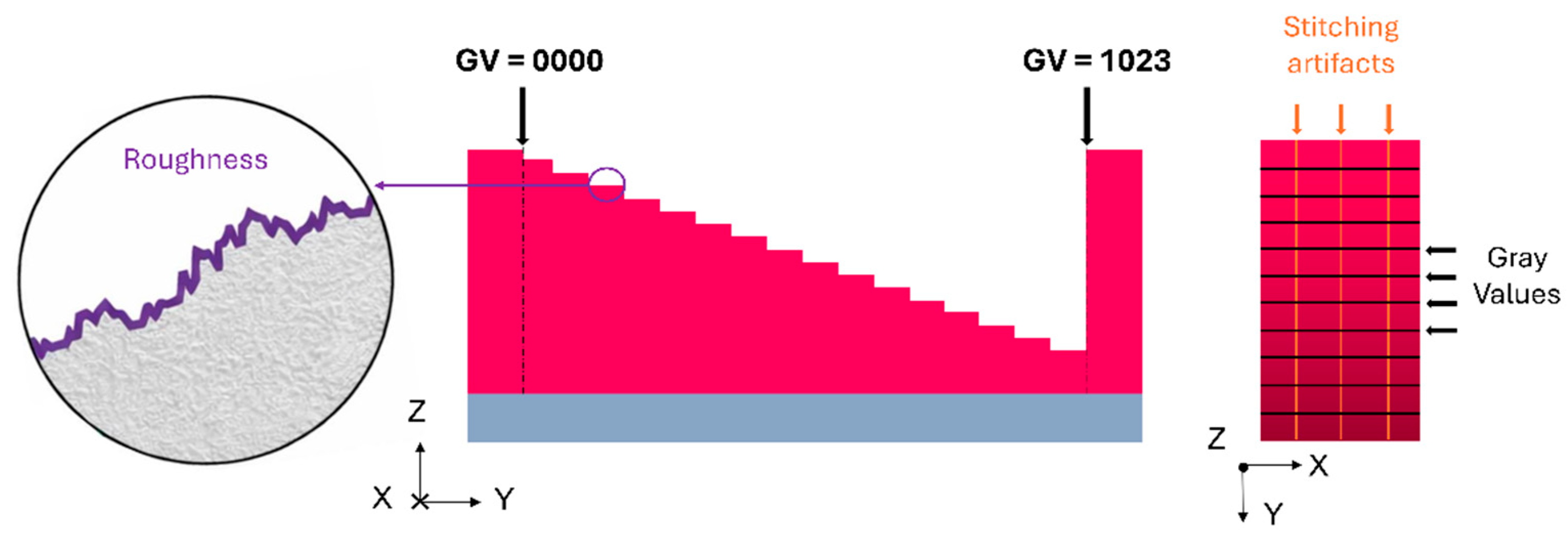
Figure 2.
(a) LSCM measurements of 15 linear slopes exposed at different laser powers with slopes descending from top to the bottom of the figure (b) Representative 2D profiles of slopes no. 3, 4, 6, 9, 11, and 13, from left to right. (c) Residuals after linear form removal. Structure written with WM III, 256 GVs and CI-over 40.
Figure 2.
(a) LSCM measurements of 15 linear slopes exposed at different laser powers with slopes descending from top to the bottom of the figure (b) Representative 2D profiles of slopes no. 3, 4, 6, 9, 11, and 13, from left to right. (c) Residuals after linear form removal. Structure written with WM III, 256 GVs and CI-over 40.
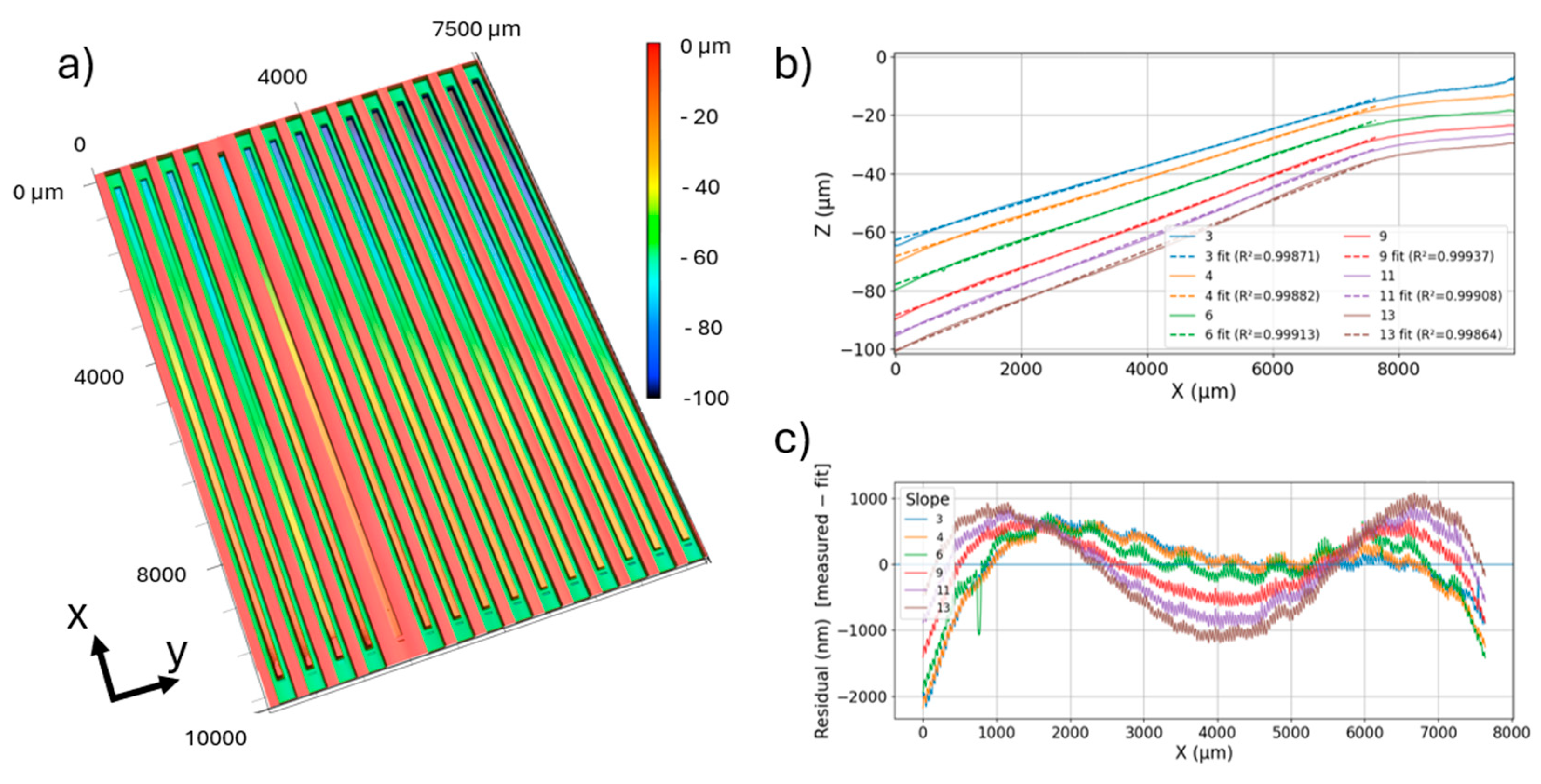
Figure 3.
(a) LSCM measurements of linear slope fabricated in mr-P 22G XP on the DWL 66+ using WM III, 256 GVs and CI-over 40. (b) 2D profile of linear slopes with different depths. (c) The lateral step spacing remains constant at ~39 μm, consistent with the imposed discretization, while the step height varies slightly due to the local change in slope angle (smaller at the beginning, larger toward the end).
Figure 3.
(a) LSCM measurements of linear slope fabricated in mr-P 22G XP on the DWL 66+ using WM III, 256 GVs and CI-over 40. (b) 2D profile of linear slopes with different depths. (c) The lateral step spacing remains constant at ~39 μm, consistent with the imposed discretization, while the step height varies slightly due to the local change in slope angle (smaller at the beginning, larger toward the end).
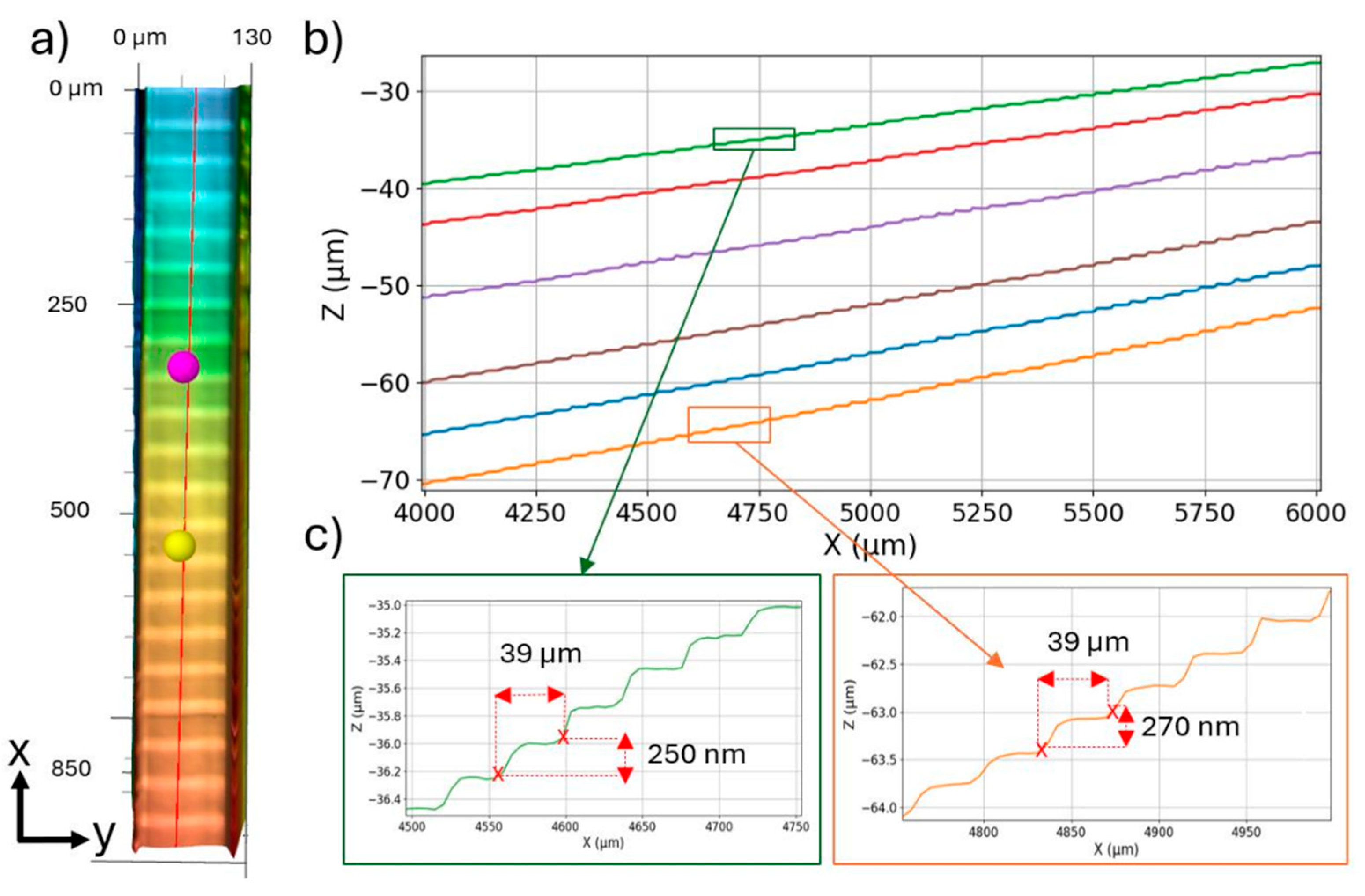
Figure 4.
Exposure artifacts on a linear slope fabricated by grayscale direct-write lithography (DWL) (a) LSCM measurements of linear slope fabricated in mr-P 22G XP on the DWL 66+ using WM III, 1024 GVs and CI-over 10. 100 µm wide slope with 256 GVs, showing stitching artifacts every 30 µm along the slope direction). (b) AFM image of the slope, the position is indicated in the LSCM image (a), with a measured total RMS roughness of 55 nm, that includes both the step and intrinsic roughness; (c) 2D profile perpendicular to the slopes, thus scanning over the stitching errors, represented by ~170 nm high steps, showing a peak and valley behavior at the border of the writing fields; (d) and (e) AFM measurements in between writing fields showing roughness of 4.1 and 4.3 nm, respectively.
Figure 4.
Exposure artifacts on a linear slope fabricated by grayscale direct-write lithography (DWL) (a) LSCM measurements of linear slope fabricated in mr-P 22G XP on the DWL 66+ using WM III, 1024 GVs and CI-over 10. 100 µm wide slope with 256 GVs, showing stitching artifacts every 30 µm along the slope direction). (b) AFM image of the slope, the position is indicated in the LSCM image (a), with a measured total RMS roughness of 55 nm, that includes both the step and intrinsic roughness; (c) 2D profile perpendicular to the slopes, thus scanning over the stitching errors, represented by ~170 nm high steps, showing a peak and valley behavior at the border of the writing fields; (d) and (e) AFM measurements in between writing fields showing roughness of 4.1 and 4.3 nm, respectively.
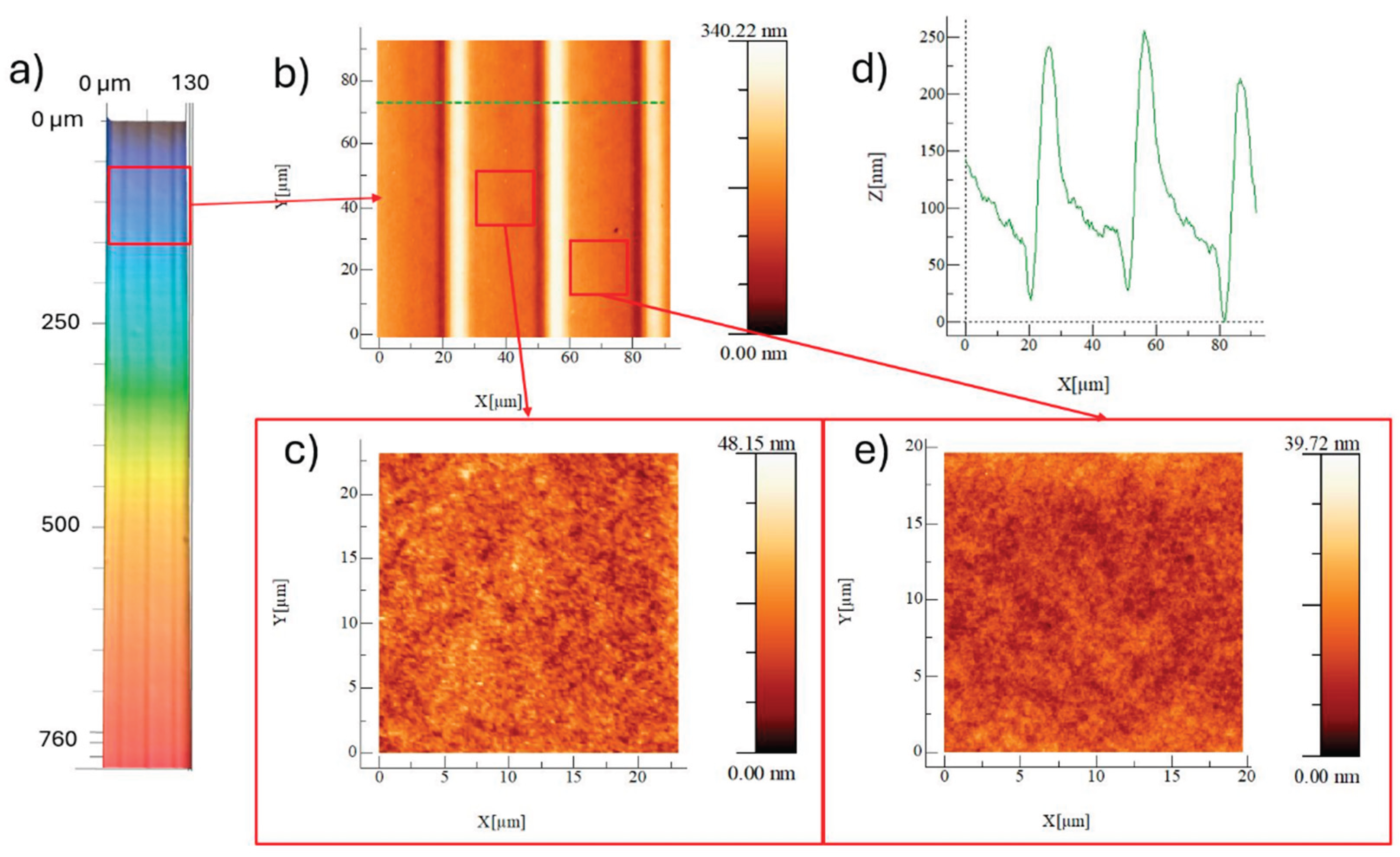
Figure 5.
(a) Linear slope fabricated by grayscale direct-write lithography (DWL). (b) and (c) AFM measurements of the linear slopes with an area of 30 x 30 µm² and 10 x 10 µm², respectively, showing a roughness of 4.4 and 4.2 nm, in line with the values obtained in Figure 4.
Figure 5.
(a) Linear slope fabricated by grayscale direct-write lithography (DWL). (b) and (c) AFM measurements of the linear slopes with an area of 30 x 30 µm² and 10 x 10 µm², respectively, showing a roughness of 4.4 and 4.2 nm, in line with the values obtained in Figure 4.
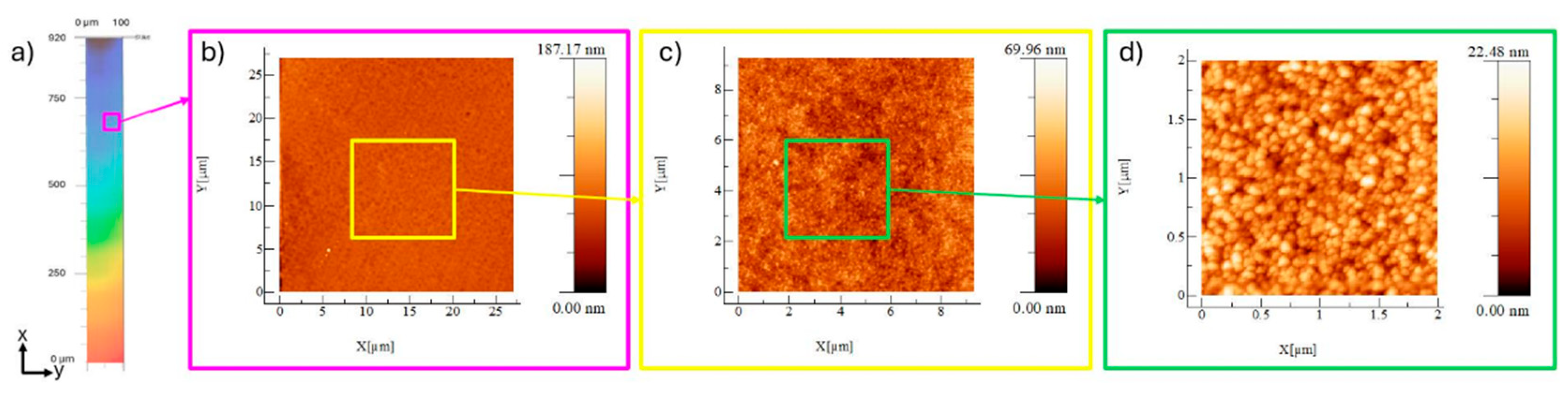
Figure 6.
AFM measurement of single crystal sapphire template with atomic-scale 0.3 nm high and 0.2 µm wide surface steps over a 1 × 1 µm² area. Inlet: 2D profile along dotted line; a) original sapphire sample. b) imprint in PMMA; c) after TASTE process. The inlet in c) shows a comparison of the 2D profile before (green) and after (orange) TASTE.
Figure 6.
AFM measurement of single crystal sapphire template with atomic-scale 0.3 nm high and 0.2 µm wide surface steps over a 1 × 1 µm² area. Inlet: 2D profile along dotted line; a) original sapphire sample. b) imprint in PMMA; c) after TASTE process. The inlet in c) shows a comparison of the 2D profile before (green) and after (orange) TASTE.
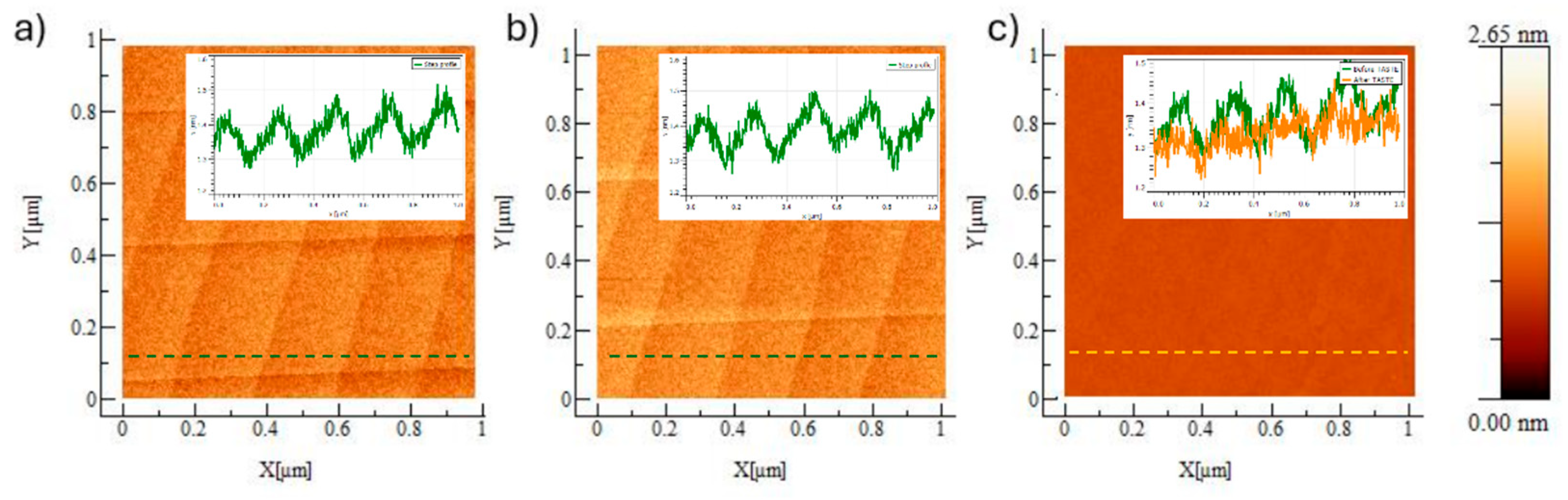
Figure 7.
2D profile of linear slopes in mr-P 22G resist and PMMA. The mr-P 22G 2D profile was intentionally vertically offset (+6 µm).
Figure 7.
2D profile of linear slopes in mr-P 22G resist and PMMA. The mr-P 22G 2D profile was intentionally vertically offset (+6 µm).
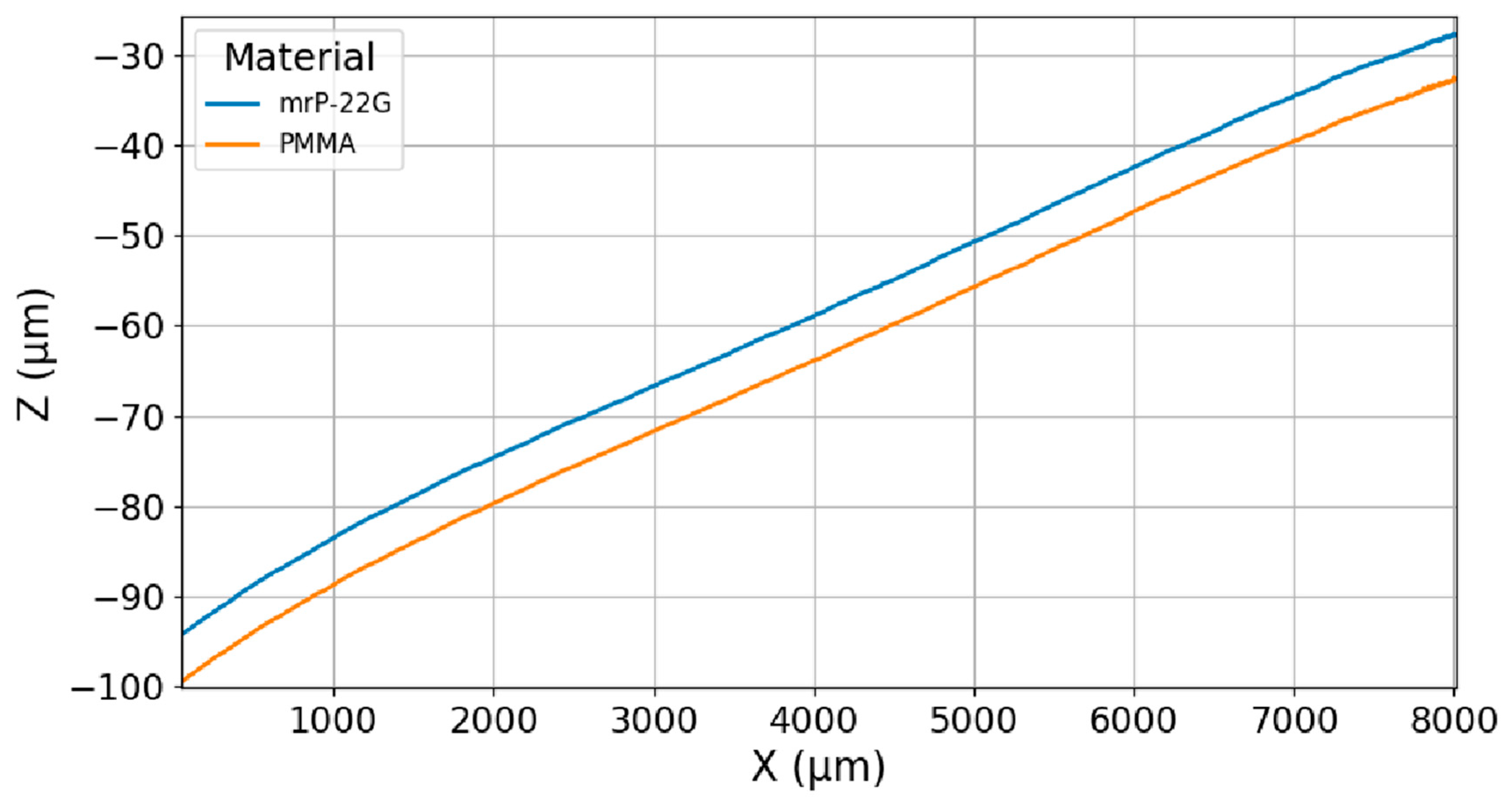
Figure 8.
(a) LSCM measurements of linear slope in PMMA, replica of linear slopes fabricated in mr-P 22G XP on the DWL 66+ using WM III, 256 GVs and CI-over 40. (b) and (d) AFM image with scan of PMMA before TASTE, the scan area is 10 x 10 µm² and 2 x 2 µm², respectively; (c) and (e) AFM image with scan of PMMA after TASTE, the scan area is 10 x 10 µm² and 2 x 2 µm², respectively.
Figure 8.
(a) LSCM measurements of linear slope in PMMA, replica of linear slopes fabricated in mr-P 22G XP on the DWL 66+ using WM III, 256 GVs and CI-over 40. (b) and (d) AFM image with scan of PMMA before TASTE, the scan area is 10 x 10 µm² and 2 x 2 µm², respectively; (c) and (e) AFM image with scan of PMMA after TASTE, the scan area is 10 x 10 µm² and 2 x 2 µm², respectively.
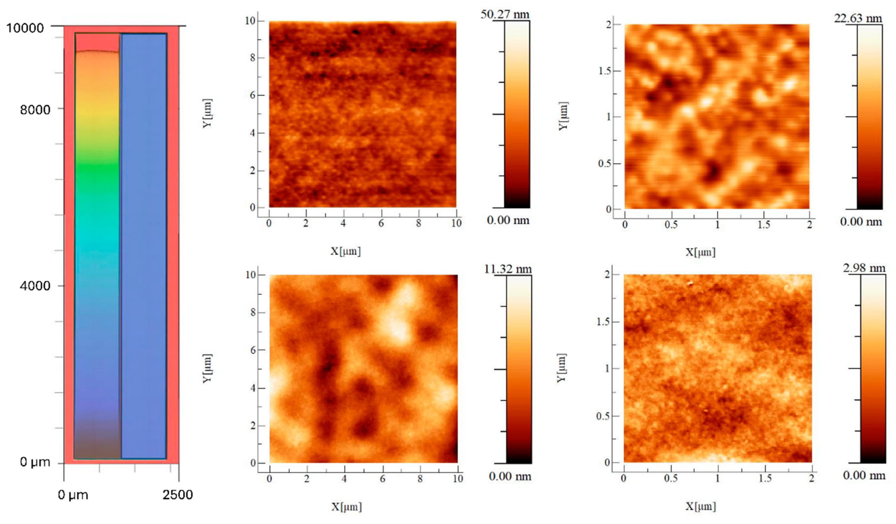
Figure 9.
AFM image of mrP 22G XP exposed with the Picomaster, the scan area is 10 x 10 µm²; (b) Histogram of heights distribution.
Figure 9.
AFM image of mrP 22G XP exposed with the Picomaster, the scan area is 10 x 10 µm²; (b) Histogram of heights distribution.
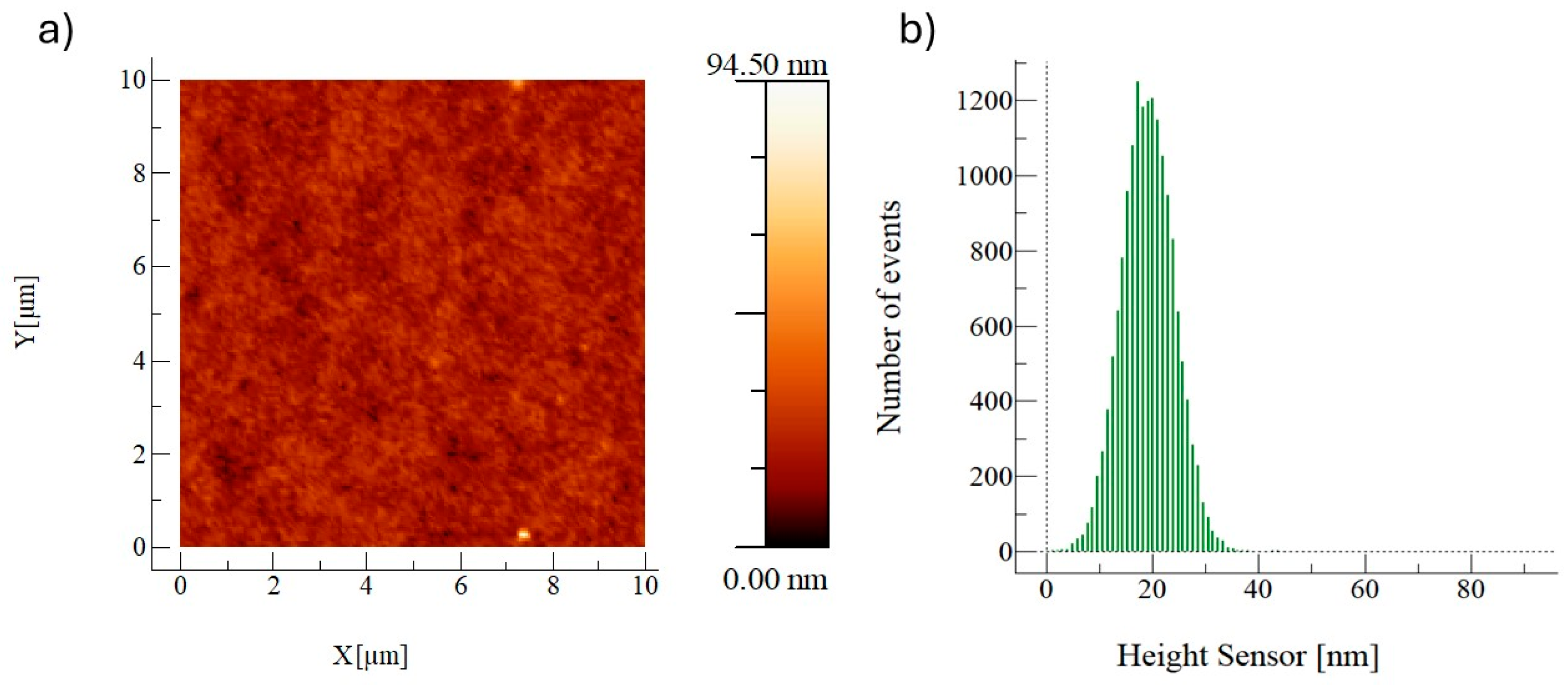
Table 2.
Quantitative evaluation of roughness through the fabrication steps from spin coating of novolak positive-tone resist to thermal reflow of the thermoplastic PMMA.
Table 2.
Quantitative evaluation of roughness through the fabrication steps from spin coating of novolak positive-tone resist to thermal reflow of the thermoplastic PMMA.
| Process step | Schematic | Material / Tool |
Main porpose |
Dominant surface contribution | Roughness / waviness (Sq) | Mitigation / optimization strategy |
| Spin coating & soft bake |  |
mr-P 22G XP | Define resist thickness (≈100 µm) | Intrinsic material roughness | 1.1 nm | Degassing, controlled bake ramp |
| Grayscale DWL exposure | 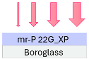 |
DWL66+ | Encode linear slope geometry | Dose discretization → waviness | 1.8 nm | Multi-pass / N-over exposure |
| Development |  |
AZ726 MIF developer | Reveal 3D topography | Stochastic development noise | < 5 nm | Dose calibration, dev. time control |
| Resist reflow |  |
mr-P 22G XP @80°C | Surface smoothening | Roughness & waviness | < 4.5 nm | — |
| Replication | 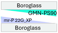 |
GMN PS90 with UV- imprint | Enable slope replication | Replication defects | < 5 nm | Optimized imprint parameters |
| Secondary replication |  |
PMMA by thermal imprint |
TASTE- compatible material | Material roughness increase | < 5 nm | Controlled embossing conditions |
| TASTE process |  |
Thermal equilibration | Reduce high- frequency roughness | Depth- selective (~200 nm) roughness reduction | 1.3 nm | Time–temperature tuning |
Disclaimer/Publisher’s Note: The statements, opinions and data contained in all publications are solely those of the individual author(s) and contributor(s) and not of MDPI and/or the editor(s). MDPI and/or the editor(s) disclaim responsibility for any injury to people or property resulting from any ideas, methods, instructions or products referred to in the content. |
© 2026 by the authors. Licensee MDPI, Basel, Switzerland. This article is an open access article distributed under the terms and conditions of the Creative Commons Attribution (CC BY) license (http://creativecommons.org/licenses/by/4.0/).
Copyright: This open access article is published under a Creative Commons CC BY 4.0 license, which permit the free download, distribution, and reuse, provided that the author and preprint are cited in any reuse.


