

Submitted:
29 June 2026
Posted:
30 June 2026
You are already at the latest version
Abstract
In all-Josephson-junction (all-JJ) logic, cell area is determined by the size of Josephson junctions, enabling intrinsically compact layouts. Tunable kinetic inductance offers a route to add circuit reconfigurability, pushing further scaling within the same all-JJ framework. In this work we present a set of basic cells for reconfigurable superconducting “kinemonics” that exploit tunable kinetic inductances of a multi-layer nanostructure to realise multiple logic functions within a single compact circuit. We then combine these gates into a universal programmable logic cell consisting of only four reconfigurable gates supplemented by a single tunable kinetic-inductance key and demonstrate that it can realise all sixteen two-input Boolean functions, making it an analogue of a look-up table with in-hardware reconfigurability. We also discuss how the same principle can be used in superconducting neuromorphic circuits, where tunable kinetic inductance controls routing, coincidence detection, inhibition, and delay for soliton-like spikes in neuron-like elements.
Keywords:
superconducting electronics
; Josephson junctions
; tunable kinetic inductors
; universal programmable logic cell
; all-JJ logic cells
; low power consumption
1. Introduction
Rapid Single-Flux Quantum (RSFQ) logic, based on the Josephson effect and magnetic flux quantization, has long been a central superconductor digital technology, combining picosecond-scale switching with very low energy dissipation [1,2,3]. As circuit complexity and integration density increase, however, the physical size of both active and passive elements becomes a major scaling constraint. In particular, inductors occupy a substantial fraction of the chip area and limit the functional density of RSFQ circuits [4].
Kinetic inductance offers a direct physical route to reducing this area penalty. In thin or nanostructured superconductors, a substantial part of the inductive energy is stored in the inertia of the superconducting condensate rather than in the magnetic field surrounding the conductor [5,6,7]. Therefore, narrow superconducting segments can provide large inductance per unit length and replace much larger geometric inductors. More broadly, kinetic inductance has become an active design resource in superconducting resonators, detectors, sensors, and quantum-circuit elements, rather than only a parasitic contribution to be minimized [8,9,10].
Beyond enabling circuit miniaturization, kinetic inductance provides additional functionality. Since it depends on the density of superconducting carriers, it can be sensitive to external stimuli and used as a functional, and in some cases tunable, circuit parameter. This principle underlies microwave kinetic inductance detectors, superconducting single-photon detectors, nonlinear kinetic-inductance sensors, tunable microwave resonators, and kinetic-inductance-based quantum elements [11,12,13,14,15,16]. For superconducting computing systems, both classical and quantum, compact kinetic-inductance elements can increase integration density and reduce parasitic magnetic crosstalk by replacing large inductive loops with local nanoscale structures [17].
In this work we use the term “superconducting kinemonics” for circuit architectures in which kinetic inductance acts as a functional control unit (variable) for SFQ-like pulse dynamics. Changing the kinetic inductance modifies the propagation, blocking, splitting, or logical combination of pulses, shifting the design philosophy from fixed superconducting wiring toward compact cells whose assignment or function can be selected after fabrication.
The term “kinemonics” also emphasizes that the proposed logic is based on controlled motion of nonlinear excitations rather than on static voltage levels. In Josephson digital circuits, a logical event is represented by a localized SFQ-like voltage pulse associated with a single magnetic flux quantum:
and by the corresponding transient redistribution of currents in the superconducting branches. In a Josephson transmission line such an excitation is often described as a fluxon or soliton-like pulse. In the lumped all-JJ cells considered here it is not an exact soliton of an integrable continuous model, but it retains the features essential for circuit operation: temporal localization, nonlinear threshold dynamics, and robust transfer from one cell to another [18]. The logic operations studied below can therefore be interpreted as controlled scattering, blocking, splitting, and threshold conversion of soliton-like SFQ events.
The use of kinetic inductors, pioneered as a route to compact superconducting digital circuits, addresses the inductor-area bottleneck but also introduces practical constraints. High-kinetic-inductance elements require tight control of film thickness, material composition or disorder, linewidth, edge quality, interface transparency, and critical-current margins, because all these factors affect the target value and spread of . Our approach therefore treats kinetic inductance not as a universal replacement for every inductive element, but as a compact control key used where tunability creates additional functionality. Fixed inductive functions are avoided where possible by relying on all-Josephson-junction cell dynamics, while tunable kinetic-inductance elements are reserved for mode selection and reconfiguration.
A possible physical implementation of such a tunable element is provided by superconducting spin-valve structures, where the relative orientation of ferromagnetic layers modifies the superconducting proximity state and can therefore change the kinetic inductance [19,20]. In circuit terms, this element acts as a kinetic-inductance control key: by switching its inductive state, the same physical cell can be assigned different logical functions. This reconfigurability increases not only the density of individual elements, but also the functional density of the whole superconducting processor, because fewer distinct circuit blocks are needed to implement a larger set of operations. It also provides a mechanism for compensating fabrication spread and adjusting operating points without redesigning the full circuit.
Here we present a set of basic cells for reconfigurable superconducting kinemonics. The library includes a controllable splitter, reconfigurable AND/OR and XOR/OR cells, and a universal programmable logic cell constructed from four reconfigurable gates and one tunable kinetic-inductance element. This universal programmable logic cell implements all sixteen two-input Boolean functions and therefore plays a role analogous to a look-up table, but with the functionality encoded in a configurable hardware basis rather than in a stored truth table.
The paper is organized as follows. Section 2 introduces the normalized Josephson-junction model and the simulation criteria used throughout the work. Section 3 presents the elementary kinetic-inductance-controlled cells: the controllable splitter, the AND/OR gate, and the XOR/OR gate. Section 4 combines these gates into a universal programmable logic cell and discusses its interpretation as a compact reconfigurable Boolean block. Section 5 explains how the same programmable primitives can be interpreted in bio-inspired spiking circuits, where Boolean functions correspond to local operations such as coincidence detection, inhibition, gating, and routing. The influence of tunable kinetic inductance on the soma dynamics of a superconducting spiking neuron is also analyzed there. Section 6 summarizes the implications of the proposed approach for compact reconfigurable digital logic and neuromorphic superconducting hardware.
2. Methodology of Modeling
The nonlinear dynamics of the proposed cells is described by the resistively and capacitively shunted Josephson-junction (RSJC) model [1]. For a conventional Josephson 0-junction, the current–phase relation below the critical current is , and the total current through the junction is expressed as
Here, is the normal resistance, and C is the capacitance of the Josephson junction. After normalisation to the critical current and the plasma frequency , the expression takes the following form:
Here, dots indicate derivatives with respect to time, t, normalized to the inverse plasma frequency, , is a damping coefficient, is a normalized critical current in case it differs from the normalising current, .
In all simulations, a logical ’1’ is represented by the arrival of a soliton-like voltage pulse at the corresponding input or output port, whereas logical ’0’ corresponds to the absence of such a pulse within the prescribed time window. A cell is considered to operate correctly if, for each input pattern, the output line produces the pulse sequence required by the target truth table and no additional switching events occur after the transient relaxation time. The inductances are expressed in normalized units,
so that changing of the kinetic inductance modifies the phase-current relation of the corresponding branch and hence the redistribution of current between the Josephson junctions during pulse propagation. The parameter maps shown below were obtained by sweeping the normalized inductances and checking this pulse-level truth-table criterion for all relevant input combinations.
3. Reconfigurable All-Josephson Junction Logic Cells
The elementary cells considered below are designed within the all-Josephson-junction (all-JJ) logic framework, in which SFQ-like pulse propagation and logic operation are governed mainly by Josephson phase dynamics, while large geometric inductors are avoided. Reconfigurability is provided by a tunable kinetic-inductance element, hereafter referred to as a kinetic-inductance control key (KICK) [21]. Changing the effective kinetic inductance of this element modifies the dynamical conditions for pulse transmission through the cell and switches the same circuit topology between two operating modes, for example AND/OR or XOR/OR. Thus, the KICK adds a compact post-fabrication control parameter to an otherwise all-JJ circuit.
In the simulations below, the KICK is treated as a tunable inductive branch with a discrete set of effective values. Microscopically, these values can be associated with different magnetic states of the described multilayer superconducting heterostructure [22,23,24,25,26], such as a spin-valve-type element, in which the proximity-controlled superfluid density changes [19,20]. Since , switching the magnetic state corresponds to switching the effective inductive state. We use this mapping at the circuit level: and define the pass and block regimes of the splitter, whereas other selected values of set the operating mode of the AND/OR and XOR/OR cells. The Josephson-junction topology is kept fixed; only the KICK state changes the dynamical conditions for SFQ-like pulse propagation through the cell.
An important practical advantage of employing tunable kinetic inductance for reconfiguration is the simplicity of control distribution. If the operation mode of a gate were instead selected by its bias current, each gate would require a dedicated current line routed to a specific internal node, which rapidly increases the wiring complexity and on-chip area overhead as the number of gates grows. Our approach simplifies the circuit layout and preserves the compactness of the all-JJ design. Hence, kinetic-inductance-based tuning offers a promising route toward area-efficient and potentially more scalable reconfiguration, as the KICK state is non-volatile and does not require a static bias line.
In the present context, superconducting kinemonics does not simply mean replacing a geometric inductor by a high-kinetic-inductance wire. Instead, it refers to circuit architectures in which kinetic inductance is used as an active design variable controlling the motion, splitting, blocking, delay, or logical combination of soliton-like pulses. For example KICK here is therefore treated as a compact tunable element whose state changes the effective dynamical threshold of a Josephson circuit without requiring a change in the active Josephson-junction layout. This distinction is important: the kinetic inductance is used not only for miniaturization, but also as a post-fabrication and, in principle, dynamically adjustable degree of freedom.
3.1. Splitter
The circuit shown in Figure 1 is a 1-to-4 splitter built from four Kinetic Inductance Controllable Keys (KICKs) connected to a single Josephson junction. In our simulations, we use all-Josephson-junction transmission lines (all-JJTLs), where a single Josephson junction replaces each inductor. The input line and each of the four output branches is implemented as an all-Josephson-junction transmission line (all-JJTL) — a design where every geometric inductor of a conventional JTL is replaced by a single Josephson junction (Figure 1(b)). The standard parameters of each all-JJTL cell are: grounded junctions with , connecting junctions with , and bias current . The KICKs allow the propagation of pulses into each line to be independently enabled or blocked by tuning their kinetic inductance.
The inductance values were selected so that each output line could be controlled independently of the others without affecting the dynamics of the processes occurring within them. Here, denotes the inductance value at which pulses pass through to the output line, while denotes the value at which pulses are blocked. Figure 2(a) presents a parameter map for possible inductance values. The yellow region indicates pairs (, ) that ensure correct operation of the splitter scheme, while the blue region corresponds to operational failure. All possible combinations of enabling/disabling the output lines were verified. An increase in the critical current of the connecting Josephson junctions, , leads to a narrowing of the operational parameter region.
3.2. AND/OR
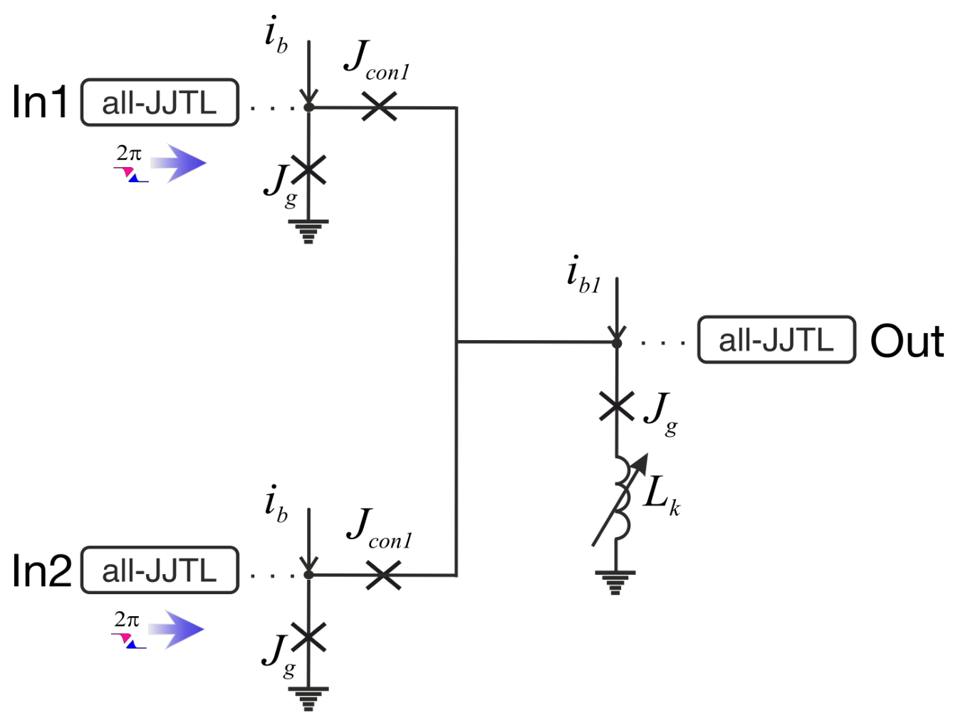
Utilizing kinetic inductance, it is possible to create a logic cell that operates as AND (for low values of inductance L) or OR (for high values of inductance L) gate. For low inductance values ( in normalized units), the inductor behaves as a weak barrier: a single input pulse cannot supply sufficient current to trigger the output junction . Only when two pulses arrive synchronously do their currents add constructively, overcoming the barrier and switching ; the cell thus operates as an AND gate. At higher inductances (), the energy storage capability of the kinetic inductor increases considerably. A single pulse now deposits energy in the kinetic inductance (the kinetic energy of the superconducting condensate), and the subsequent release of this stored energy provides an additional current surge that drives well above its critical value. In this regime the cell fires upon receiving any input, behaving as an OR gate. A further increase of beyond the value leads to the formation of several stable states and gives rise to other complex dynamics.
Figure 3.
Circuit diagram of a cell with controlled kinetic inductance for switching the circuit’s operation mode between AND and OR logic gates. : . .
Figure 3.
Circuit diagram of a cell with controlled kinetic inductance for switching the circuit’s operation mode between AND and OR logic gates. : . .
3.3. XOR/OR
The addition of kinetic inductance enables the cell to function as an XOR gate at and as an OR gate at (see Figure 4).
In this cell the junction acts as a coincidence-triggered blocking element: a phase slip of disrupts the propagating soliton-like pulse and prevents it from reaching the output. Because the current driven through this branch scales inversely with the series inductance, , the value of sets the effective threshold for switching . For low inductance values ( in normalized units), the current delivered to by a single input pulse stays below its critical value, so remains superconducting and the pulse propagates to the output. When two pulses arrive synchronously, the contributions from the two junctions add at the common node, the current through exceeds its critical value, and undergoes a slip that halts the soliton. The output thus fires for exactly one active input and is suppressed for two coincident inputs, so the cell operates as an XOR gate. For higher inductances (), the series kinetic inductance limits the current reaching below its critical value even for two coincident pulses. The junction can therefore no longer switch, the blocking mechanism is disabled, and every input — single or coincident — propagates to the output. In this regime the cell operates as an OR gate.
We also demonstrate that the functionality of the XOR gate can be further enriched by introducing two additional kinetic inductances into the circuit. The circuit in Figure 5 can be reconfigured to realise the asymmetric function ; specifically, this requires setting and (the mirrored function is obtained analogously by swapping inductance settings). This transformation is achieved solely by tuning the kinetic inductance values, without any changes to the active Josephson junctions or the addition of new bias lines. The ability to realise the non-commutative function is particularly attractive for neuromorphic or bio-inspired spiking neural networks. In such systems, the directionality of synaptic connections plays a fundamental role: the postsynaptic neuron C may be required to respond to a spike from the neuron B only when the presynaptic neuron A has not fired recently, implementing a form of gated inhibition or a directional receptive field. This operation naturally arises in circuits mimicking spike-timing-dependent plasticity (STDP), where the relative order of pre- and postsynaptic events determines whether a synapse is potentiated or depressed, or in Winner-Take-All architectures, where the activity of one input must selectively suppress or gate another.
4. Reconfigurable Logic Basis and Universal Programmable Cell
Building upon the fundamental AND/OR and XOR/OR gates with controllable kinetic inductance, we propose a novel architecture for a universal programmable logic cell. While the individual reconfigurable gates do not constitute a complete logical basis, the incorporation of a constant logical "1" enables the implementation of inversion functionality through XOR operations, thereby forming a universal set.
The proposed architecture, illustrated in Figure 6, represents an analog of a Look-Up Table (LUT) commonly used in FPGA architectures. However, instead of storing precomputed truth tables in memory, our approach implements a configurable logical basis where the functionality is defined by the operational modes of the kinetic inductance gates. This provides dynamic reconfigurability at the hardware level while maintaining the performance benefits of superconducting electronics.
Through exhaustive computational analysis of all possible gate combinations, we have determined that four reconfigurable gates, supplemented by a tunable kinetic-inductance key on one of the internal signal lines, are sufficient to implement all 16 possible two-input Boolean functions. To identify the minimal gate-level topology capable of realising all sixteen two-input Boolean functions, we performed an exhaustive depth-first search over feed-forward circuits built from reconfigurable AND/OR and XOR/OR gates. The available signal sources are the primary inputs A and B, a constant logical “1”, and the outputs of all previously placed gates. For a fixed total number of gates N, the search recursively constructs a circuit by assigning to each gate:
- 1.
- two input signals chosen from the admissible set, and
- 2.
- a gate type, either AND/OR or XOR/OR.
Once a complete N-gate topology is assembled, its functional coverage is evaluated. For every combination of the gates’ configuration bits (there are possibilities, each selecting the current operating mode of a gate), the output of the circuit is computed for the four input patterns . The set of distinct truth tables obtained across all configurations forms the coverage mask of the topology. If the mask contains all 16 possible Boolean functions, the circuit is declared universal and the search terminates. If no universal circuit with N gates exists, the search proceeds to gates; since the gate count is increased only after the exhaustive search at the current N fails, the first universal circuit found is guaranteed to use the minimal number of gates.
The optimal configuration comprises two XOR/OR gates and two AND/OR gates arranged in the topology shown in Figure 6, supplemented by a splitter at input A. The splitter distributes the signal into three lines; in one of these lines a tunable kinetic inductance is inserted. This arrangement ensures maximal functional coverage while minimizing the component count and maintaining signal integrity throughout the circuit.
Figure 6.
(a) Architecture of the universal programmable logic cell based on reconfigurable all-JJ gates. The circuit consists of four reconfigurable gates (XOR/OR and AND/OR types) and utilizes a constant logical "1" for inversion operations. A splitter at input A distributes the signal, and a tunable kinetic inductance in one of its branches acts as an additional programmable element with two states: pass and block. Together with the four gates, the state of this inductance determines which Boolean function is realised. (b) Circuit-level schematic of the same cell at the Josephson-junction level, showing the individual junctions, bias currents and KICK elements. The parameters of the splitter and of all four gates are listed in Table 1.
Figure 6.
(a) Architecture of the universal programmable logic cell based on reconfigurable all-JJ gates. The circuit consists of four reconfigurable gates (XOR/OR and AND/OR types) and utilizes a constant logical "1" for inversion operations. A splitter at input A distributes the signal, and a tunable kinetic inductance in one of its branches acts as an additional programmable element with two states: pass and block. Together with the four gates, the state of this inductance determines which Boolean function is realised. (b) Circuit-level schematic of the same cell at the Josephson-junction level, showing the individual junctions, bias currents and KICK elements. The parameters of the splitter and of all four gates are listed in Table 1.
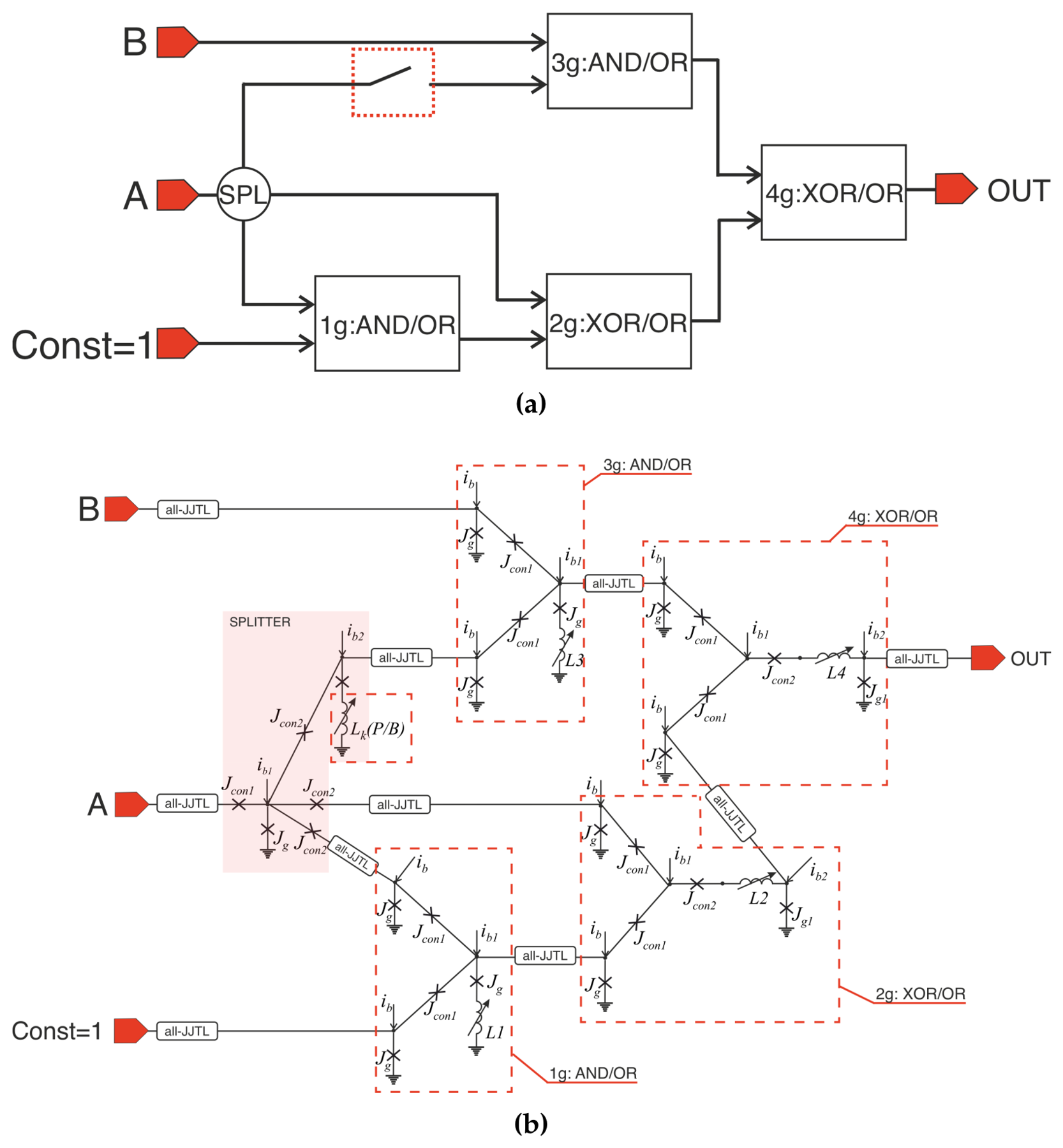

Table 1.
Parameters of the splitter and the four reconfigurable gates of the universal programmable cell (Figure 6). Junction critical currents are given as normalized amplitudes ; bias currents are normalized to . A dash denotes an element absent in the given cell.
Table 1.
Parameters of the splitter and the four reconfigurable gates of the universal programmable cell (Figure 6). Junction critical currents are given as normalized amplitudes ; bias currents are normalized to . A dash denotes an element absent in the given cell.
| Cell | Type | |||||
|---|---|---|---|---|---|---|
| Splitter | 1-to-3 | 0.7 | 0.3 | 1.0 | 1.0 | 0.95 |
| , | XOR/OR | 0.6 | 0.75 | 0.25 | 0.6 | 0.25 |
| , | AND/OR | 0.3 | – | 1.0 | 1.2 | – |
The programmable cell is configured by setting the state of five tunable kinetic inductances: one in the splitter (pass or block) and one in each of the four gates, which determines their operational mode (AND/OR or XOR/OR). This configurability enables the same physical circuit to implement diverse logical functions, including but not limited to: AND, OR, XOR, NAND, NOR, XNOR, and various implication functions.
Potential applications of this technology include:
- dynamically reconfigurable superconducting processors for adaptive computing;
- energy-efficient neuromorphic computing systems requiring programmable connectivity;
- quantum-classical interface circuits with adaptable signal processing capabilities.
The universal cell described earlier requires an external constant “1” line to implement inversion within the logic fabric. A more compact and self-contained variant can be obtained by placing a single D-flip-flop with complementary outputs on only one of the primary inputs, for instance on input A. The flip-flop stores the logical value of A and simultaneously provides both the true (A) and inverted () versions of this variable. A constant “1” is then generated internally by feeding A and into additional AND/OR gate configured as an OR gate; as long as the clocked data is held, the output of this OR remains a stable logical “1”. D-flip-flops with complementary outputs are standard primitives in superconducting digital libraries (the RSFQ DRO intrinsically offers both true and inverted outputs), so the modification introduces no fabrication overhead. The topology of the original four-gate universal block remains unchanged; the only difference lies in the way the internal signal pool is created. This arrangement makes the cell autonomous, preserves all sixteen two-input Boolean functions with the same configuration table, and enhances regularity for large-scale reconfigurable systems.
For clarity, we encode each configuration of the universal programmable cell by a five-letter word corresponding to the operating modes of a kinetic inductance and gates 1–4 in Figure 6. For the XOR/OR gates, the letter (X) denotes the XOR mode and (O) denotes the OR mode; for the AND/OR gates, the letter (A) denotes the AND mode and (O) denotes the OR mode; for the tunable kinetic inductance in the splitter line, the letter (P) denotes the pass state (high ) and (B) denotes the block state (low ). Thus a configuration word specifies a particular hardware state of the five tunable kinetic-inductance elements. Sweeping all such configuration words produces the full set of sixteen two-input Boolean functions. This representation is useful because it makes the programmable cell closer to a small reconfigurable logic fabric than to a conventional memory-based LUT: the function is selected by physical operating modes of gates rather than by reading a stored truth table.
Table 2.
Truth table of all two-input Boolean functions and their relevance to bio-inspired spiking neural networks. Functions are grouped by symmetry and potential use in neuromorphic circuits.
Table 2.
Truth table of all two-input Boolean functions and their relevance to bio-inspired spiking neural networks. Functions are grouped by symmetry and potential use in neuromorphic circuits.
| Inputs (A,B) | ||||||
|---|---|---|---|---|---|---|
| (0,0) | (0,1) | (1,0) | (1,1) | Function | Configured mode | Neuromorphic relevance |
| Constant functions | ||||||
| 0 | 0 | 0 | 0 | FALSE | BAXAX, BAXAO | Complete inhibition (silent) |
| 1 | 1 | 1 | 1 | TRUE | BOOAX, BOOAO, BOOOO, POXOO, POOAO, POOOO | Tonic excitation |
| Symmetric functions | ||||||
| 0 | 0 | 0 | 1 | AND | PAXAX, PAXAO | Coincidence detection |
| 0 | 1 | 1 | 1 | OR | BAOOO, PAXOX, PAXOO, PAOOO | Input integration |
| 0 | 1 | 1 | 0 | XOR | BAOOX | Coincidence/ anti-coincidence (STDP) |
| 1 | 1 | 1 | 0 | NAND | POOAX | Universal gate |
| 1 | 0 | 0 | 0 | NOR | POOOX | Universal gate |
| 1 | 0 | 0 | 1 | XNOR | BOXOX | Equivalence detection |
| Projection and inversion | ||||||
| 0 | 0 | 1 | 1 | A | BAOAX, BAOAO, PAOAO | Signal pass-through |
| 0 | 1 | 0 | 1 | B | BAXOX, BAXOO | Signal pass-through |
| 1 | 1 | 0 | 0 | NOT A | BOXAX, BOXAO | Inversion |
| 1 | 0 | 1 | 0 | NOT B | BOOOX | Inversion |
| Asymmetric (inhibition / implication) | ||||||
| 0 | 0 | 1 | 0 | PAOAX | Directional gating, lateral inhibition | |
| 0 | 1 | 0 | 0 | PAOOX | Directional gating, lateral inhibition | |
| 1 | 0 | 1 | 1 | POXOX | Conditional activation | |
| 1 | 1 | 0 | 1 | BOXOO, POXAX, POXAO | Conditional activation | |
5. Kinetic Inductances in Spiking Neural Network Elements
Kinetic inductance can also be used in superconducting neuromorphic circuits [27,28,29,30], in particular in bio-inspired spiking neural networks[28,31]. This neuromorphic extension is consistent with the broader view that superconducting electronics can provide ultrafast, low-dissipation hardware for spike-based computation [32], while Josephson junctions naturally support neuron-like threshold, spiking, and bursting dynamics [27,33,34]. In such systems, the main functional elements are the neuron’s soma, the axon-like transmission line, and the synaptic connection. Replacing geometric inductances by tunable kinetic inductances can reduce the occupied area, improve scalability, and suppress parasitic magnetic coupling associated with large inductive loops. At the same time, kinetic inductance provides an additional control parameter for tuning thresholds, propagation delays, and dynamical regimes of spiking elements as demonstrated in Figure 7 and Figure 8.
At the same time the neuromorphic relevance of the universal programmable cell should not be understood as a direct one-to-one mapping between Boolean gates and biological neurons. Instead, the cell provides a compact library of local event-driven operations that are repeatedly needed in spiking neural hardware. In such systems, spikes must be combined, suppressed, delayed, routed, and conditionally transmitted. Boolean functions naturally describe these local operations at the level of pulse presence or absence within a timing window. For example, AND gate implements coincidence detection, OR gate implements input integration, XOR gate implements anti-coincidence or mismatch detection, and asymmetric functions such as implement inhibition or conditional routing.
This interpretation also explains why reconfigurability is especially natural in neuromorphic applications. Unlike conventional fixed digital logic, neuromorphic circuits often require changes of effective connectivity, receptive windows, inhibition patterns, and routing rules. A kinetic-inductance-controlled cell can therefore serve as a local programmable element whose function can be adapted without redesigning the circuit layout. In this sense, the same universal cell bridges conventional Boolean logic and spike-based neuromorphic processing.
5.1. Neuromorphic Applications of the Universal Programmable Cell
As previously noted, the proposed universal cell can be used for a variety of neuromorphic applications. Furthermore, to utilize it in neuromorphic or bio-inspired systems, it is not necessary to implement all 16 Boolean operations, which significantly simplifies the cell’s configuration and fabrication. In this subsection, we have endeavored to provide a fairly comprehensive overview of the potential applications of the universal cell in different ’logical states’ that are related to the functioning of living neural structures and the underlying mechanisms.
For greater convenience, we will categorize the possible applications by logical Boolean functions that the Universal Programmable Cell (UPC) can realize.
-
Implementation of simple summation of neural signals at the input of a postsynaptic neuron, where both input signals, even individually, exceed the neuron’s threshold value.
-
This mode could be used to emulate spontaneous activity, suppressed by any input.
-
Long-Term Potentiation (LTP). One of the mechanisms of Spike-timing-dependent plasticity (STDP). The idea is as follows: suppose there is a signal that needs to be transmitted between two neurons via a synaptic connection. To implement STDP, we split signal into two identical signals, A and B, which we feed into the input of a universal block. The signal B is applied with a delay of . Consequently, the output of the block will produce a signal corresponding to the intersection () of two copies of the same signal, offset by the amount of .Spatial/Temporal summation (Threshold activation). The UPC only transmits a signal when signals A and B are received synchronously at its input.Coincidence Detection. The operating principle is similar to that of LTP, but the UPC receives two different signals: if both arrive simultaneously, the UPC generates an output signal, otherwise, it generates nothing.Associative learning. Similar to a coincidence detector, but used for Hebbian learning mechanism.
-
Conscious control of reflex actions, where decisions are made automatically at the spinal cord level but can be further controlled at the brain level. For example, the act of holding a cup of hot tea in your hands. On the one side, the body tries to let go of the cup to relieve the pain, but the brain realizes that if it does so, the cup will break and the tea will spill, so it forces the body to hold the hot cup (signals 1 and 1). At the same time, if there is no cup, then there is nothing to decide (0,0). If the brain does not interfere with the spinal cord’s function, the hand will naturally relax and the cup will fall (1,0). Similarly, even if the cup is cold, the brain may send a signal to relax the fingers, leading to the expected result (0,1).
-
(inhibition, i.e. the negation of the implication )Long-Term Depression (LTD) or the saturation effect. The second STDP mechanism, which plays a crucial role in signal transmission between neurons, alongside LTP. The UPC input receives two signals: A and B, with B delayed by a time . Since the UPC is configured to implement the inhibition function , a signal with a duration of will be generated at the block’s output. In other words, signal B is the cut-off of signal A.Temporal Filtering/Receptive Windows. Conceptually, this is the same implementation as for the LTD case. Here, delay control is added: a short time window results in high signal selectivity, while a long window leads to integration. This is another mechanism, alongside STDP, that allows for the tuning of a neuron’s temporal memory.Inhibiting activity. Being in decrement mode, the UPC can mimic the behavior of a single inhibitory neuron. If we assume that input A corresponds to the signal from an excitatory neuron and input B corresponds to the signal from a conditionally inhibitory neuron, then when the two signals are synchronized, the system’s output will always be zero. If there is no signal at input B, signal A will pass through the block.Winner-Take-All. Suppose we have several UPC whose inputs are responsible for transmitting excitatory signals, and whose inputs are responsible for inhibitory signals. Then, if we feed the output signal of each UPC to the inhibitory input of all other blocks, we obtain a Winner-Take-All mode: the block that received the excitatory signal first wins (its signal can proceed further). Such a circuit paves the way for modeling competition processes, lateral inhibition, and selectivity.Realization of the refractory period. The UPC output signal is supplied to its inhibiting input B via a feedback delay circuit. Thus, the signal received at input A temporarily prevents the block from being reactivated.Oscillatory Dynamics / Rhythmogenesis / Synchronization. By connecting several blocks via delay lines and adding excitation and inhibition signals (A and B), it is possible to emulate steady-state oscillations, burst dynamics, and phase locking, which paves the way for modeling brain rhythms.
-
with ()Full STDP mechanism realization (LTP and LTD). The combination of the LTP and LTD mechanisms described above, where the output of the LTP circuit serves as the input signal for LTD. The signal B from the LTP circuit, delayed by a time constant , is used as the signal for LTD. Using this type of circuit prevents signal A from passing indefinitely and emulates the effect of a decrease in neurotransmitter concentration in the synaptic gap (the fatigue effect).Spike-Timing Routing. Implementation of a system for controlling the arrival delay of spikes in complex circuits using STDP mechanisms.
5.2. Kinetic Inductance in the Neuron Soma
The neuron soma is the part of a spiking element where the input stimulus is integrated and converted into an output voltage spike. Earlier, we proposed a superconducting bio-inspired neuron intended for operation in spiking neuromorphic networks [35] that emulate basic patterns of biological neural activity. In that design, the dynamical regime of the neuron is controlled by the circuit parameters and by the external bias current . Since the generation of an output voltage spike is determined by the phase dynamics of the Josephson circuit, replacing selected geometric inductances by kinetic inductances offers a direct way to tune the soma dynamics after fabrication.
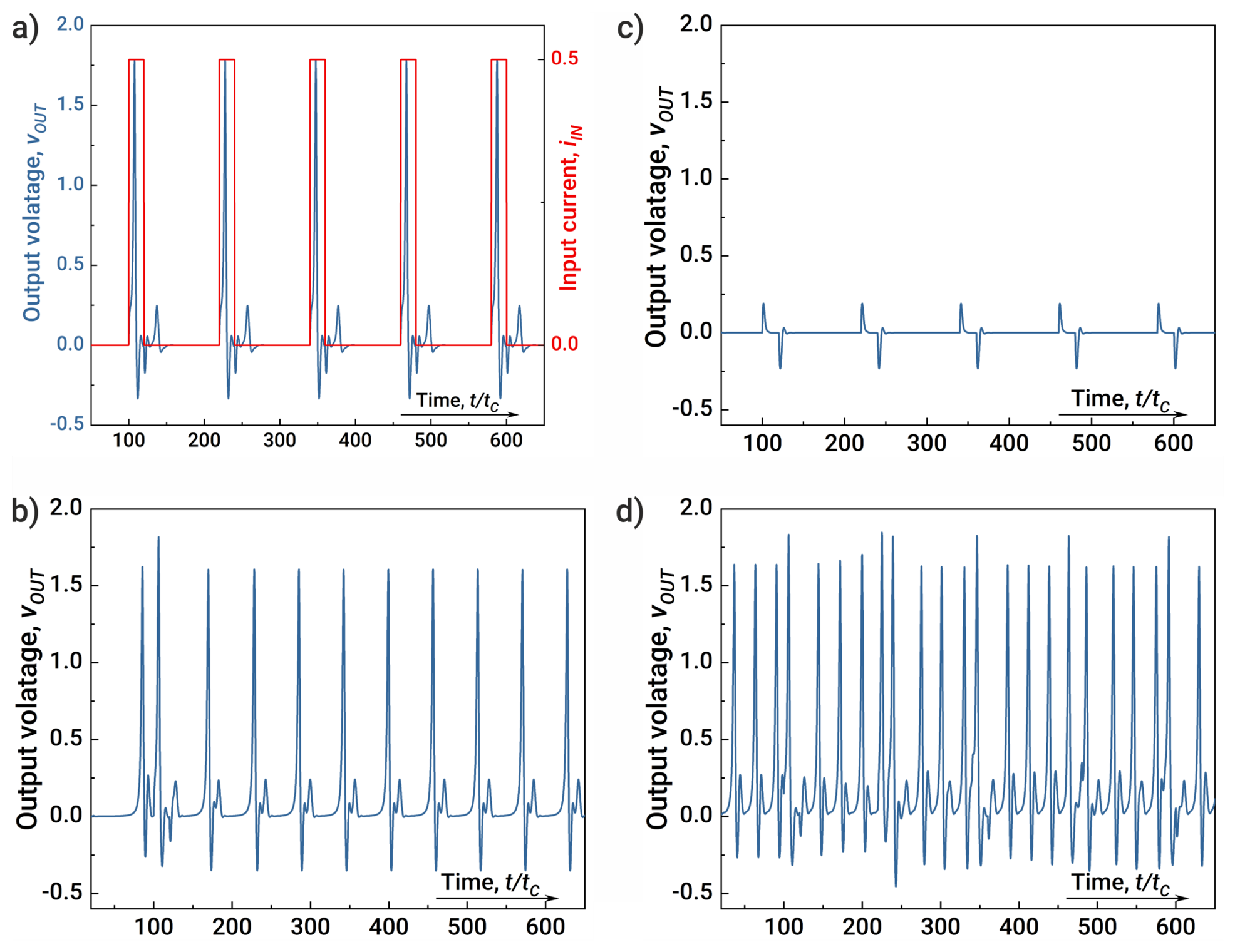
Taking the parameters of the regular mode of a spiking bio-inspired neuron from [31] as a basis and replacing the geometric inductances l, and () in the neuron’s soma with kinetic ones we have observed how the neuron’s operating regimes changed during kinetic inductance variation. The reference point was based on the following parameter values: , Josephson damping parameters (in [31] they were designated by ), and . Note that a sequence of rectangular pulses at the input with a total level , period and duration of one pulse was used as an external stimulus (here is the inverse plasma frequency, defined in the Section 2). Varying the indicated kinetic inductances with the other parameters fixed revealed three basic modes of neuron operation: regular mode (RM), steady state mode (SSM) and bursting mode (BM). In Figure 8 all the mentioned modes are marked with the corresponding designations. A separate area is occupied by the so-called non-biological mode of operation (NBM), which is characterised by continuous generation of spikes without any external influence (no input stimulus signal) and pattern activity. Typical spike-generation patterns of the neuron in all four regimes are shown in Figure 9.
6. Discussion and Conclusions
We have presented a compact set of basic cells for reconfigurable superconducting kinemonics, where kinetic inductance is used not only as a replacement for bulky geometric inductors but also as a functional control parameter. The proposed cells include a controllable splitter and two reconfigurable logic gates, AND/OR and XOR/OR. In each case, changing the kinetic inductance modifies the propagation of SFQ-like pulses and selects the operating mode of the same physical circuit.
Combining these elementary cells, we constructed a universal programmable logic cell consisting of four reconfigurable gates and a single tunable kinetic-inductance key. The cell can implement all sixteen two-input Boolean functions and therefore provides a superconducting analogue of a look-up table. In contrast to a conventional LUT, however, the functionality is not stored as a truth table in memory; it is defined by the selected modes of the kinetic-inductance-controlled gates. This makes the proposed architecture attractive for dense superconducting circuits where functional density, compactness, and post-fabrication tunability are equally important.
We also considered the role of kinetic inductance in superconducting spiking-neuron elements. In the neuron soma, replacing selected geometric inductances by kinetic inductances allows one to tune the dynamical regime of the circuit and to shift the boundaries between regular spiking, steady-state, bursting, and self-oscillatory operation. Thus, the same design principle can be used both in reconfigurable digital logic and in bio-inspired superconducting neuromorphic circuits.
The main practical advantage of this approach is the simultaneous reduction of footprint and parasitic magnetic coupling. Smaller inductive loops reduce unwanted flux cross-talk, while tunable kinetic inductance provides an additional degree of freedom for compensating fabrication spread and adjusting the circuit after fabrication. The present results are based on numerical modelling; the experimental outlook is summarized at the end of this section.
The relevant scaling metric is therefore not only the physical area of an individual inductor, but also the functional density of the circuit, i.e., the number of distinct operations that can be implemented per unit area and per active circuit element. A fixed superconducting logic library increases functional density mainly by shrinking individual cells. A reconfigurable library adds a second mechanism: the same physical cell can be assigned different logical roles in different parts of a circuit or at different stages of operation. In this sense, kinetic-inductance tuning provides a hardware-level analogue of programmability, while preserving the picosecond-scale pulse dynamics and low dissipation characteristic of Josephson logic.
The proposed architecture also clarifies the relation between conventional digital superconducting logic and neuromorphic superconducting circuits. In the digital interpretation, the universal programmable cell is a compact reconfigurable Boolean primitive: it implements all sixteen two-input functions and can therefore be used as a hardware analogue of a small LUT. In the neuromorphic interpretation, the same set of functions describes local spike-processing motifs: coincidence detection, inhibition, conditional transmission, routing, refractory blocking, and winner-take-all competition. Thus the digital and neuromorphic uses are not separate applications of unrelated devices; they are two interpretations of the same kinetic-inductance-controlled pulse logic.
This point is important because reconfigurability has a different status in the two cases. For conventional digital logic, reconfigurability is a route to higher functional density, post-fabrication correction of parameter spread, and reduced need for specialized cells. For neuromorphic hardware, reconfigurability is even more fundamental: adaptation, plasticity, and task-dependent connectivity are intrinsic parts of the computational model. A fixed superconducting spiking network would be limited to one hard-wired architecture, whereas a network built from reconfigurable kinemonic cells can modify local gating rules and effective inter-neuron connections directly on chip.
Therefore, tunable kinetic inductance provides more than a compact replacement for geometric inductors. It supplies a physically natural control variable for superconducting hardware in which compactness, low dissipation, and programmability must coexist. The next essential step is an experimental demonstration of the proposed KICK-based cells, including measurements of switching margins, timing jitter, parameter tolerance, reprogramming stability, and multi-cell operation. Such experiments will determine the practical operating window of superconducting kinemonics and its prospects as a common hardware platform for dense reconfigurable logic and cryogenic spiking neural networks.
Author Contributions
Conceptualisation, V.I.R., N.V.K., and I.I.S.; Data curation, N.V.K.; Formal analysis, N.V.K.; Methodology, V.I.R.; Software, A.A.M.; Investigation, V.I.R., A.A.M.; Supervision, I.I.S., M.V.T.; Validation, I.I.S., A.E.S., and V.I.R.; Visualisation, A.A.M.; Funding acquisition, I.I.S., M.V.T; Writing—original draft, A.E.S., N.V.K. and A.A.M.; Writing—review and editing, M.V.T. and S.V.B. All authors have read and agreed to the published version of the manuscript.
Funding
The development of the main concept of reconfigurable cells was supported by the Russian Science Foundation, Russia, Grant No. 24-19-00187. The study of the basic element for kinemonic-based neuronetworks was supported by Ministry of Science and Higher Education (agreement No. 075-15-2024-538). A.A.M. is grateful to the Foundation for the Advancement of Theoretical Physics and Mathematics "BASIS" (grant 24-2-10-6-1).
Data Availability Statement
All relevant data are included in the article.
Conflicts of Interest
The authors declare no conflict of interest. The funders had no role in the design of the study; in the collection, analyses, or interpretation of data; in the writing of the manuscript; or in the decision to publish the results.
References
- Likharev, K.K.; Semenov, V.K. RSFQ logic/memory family: a new Josephson-junction technology for sub-terahertz-clock-frequency digital systems. IEEE Transactions on Applied Superconductivity 1991, 1, 3–28. [CrossRef]
- Likharev, K.K. Superconductor digital electronics. Physica C: Superconductivity and its Applications 2012, 482, 6–18. [CrossRef]
- Holmes, D.S.; Ripple, A.L.; Manheimer, M.A. Energy-efficient superconducting computing—power budgets and requirements. IEEE Transactions on Applied Superconductivity 2013, 23, 1701610. [CrossRef]
- Tolpygo, S.K. Superconductor digital electronics: scalability and energy efficiency issues. Low Temperature Physics 2016, 42, 361–379. [CrossRef]
- Annunziata, A.J.; Santavicca, D.F.; Frunzio, L.; Catelani, G.; Rooks, M.J.; Frydman, A.; Prober, D.E. Tunable superconducting nanoinductors. Nanotechnology 2010, 21, 445202. [CrossRef]
- Tolpygo, S.K.; Bolkhovsky, V.; Oates, D.E.; Rastogi, R.; Zarr, S.; Day, A.L.; Weir, T.J.; Wynn, A.; Johnson, L.M. Superconductor electronics fabrication process with MoNx kinetic inductors and self-shunted Josephson junctions. IEEE Transactions on Applied Superconductivity 2018, 28, 1–12. [CrossRef]
- Tolpygo, S.K.; Golden, E.B.; Weir, T.J.; Bolkhovsky, V. Inductance of superconductor integrated circuit features with sizes down to 120 nm. Superconductor Science and Technology 2021, 34, 085005. [CrossRef]
- Vissers, M.R.; Gao, J.; Sandberg, M.; Duff, S.M.; Wisbey, D.S.; Irwin, K.D.; Pappas, D.P. Proximity-coupled Ti/TiN multilayers for use in kinetic inductance detectors. Applied Physics Letters 2013, 102. [CrossRef]
- Niepce, D.; Burnett, J.; Bylander, J. High kinetic inductance NbN nanowire superinductors. Physical Review Applied 2019, 11, 044014. [CrossRef]
- Grünhaupt, L.; et al. Granular aluminium as a superconducting material for high-impedance quantum circuits. Nature Materials 2019, 18, 816–819. [CrossRef]
- Day, P.K.; LeDuc, H.G.; Mazin, B.A.; Vayonakis, A.; Zmuidzinas, J. A broadband superconducting detector suitable for use in large arrays. Nature 2003, 425, 817–821. [CrossRef]
- Natarajan, C.M.; Tanner, M.G.; Hadfield, R.H. Superconducting nanowire single-photon detectors: physics and applications. Superconductor science and technology 2012, 25, 063001. [CrossRef]
- Vodolazov, D.Y. Nonlinear Kinetic Inductance Sensor. JETP Letters 2023, 118, 773–778. [CrossRef]
- Szypryt, P.; Bennett, D.A.; Fogarty Florang, I.; Fowler, J.W.; Giachero, A.; Hummatov, R.; Lita, A.E.; Mates, J.A.; Nam, S.W.; O’Neil, G.C.; et al. Kinetic inductance current sensor for visible to near-infrared wavelength transition-edge sensor readout. Communications Engineering 2024, 3, 160.
- Kalacheva, D.; Fedorov, G.; Khrapach, I.; Astafiev, O. Coplanar superconducting resonators with nonlinear kinetic inductance bridge. Superconductor Science and Technology 2023, 36, 055011. [CrossRef]
- Kalacheva, D.; Fedorov, G.; Zotova, J.; Kadyrmetov, S.; Kirkovskii, A.; Dmitriev, A.; Astafiev, O. Kinemon: An inductively shunted transmon artificial atom. Physical Review Applied 2024, 21, 024058. [CrossRef]
- Hazard, T.M.; et al. Nanowire Superinductance Fluxonium Qubit. Physical Review Letters 2019, 122, 010504. [CrossRef]
- Maksimovskaya, A.A.; Ruzhickiy, V.I.; Klenov, N.V.; Schegolev, A.E.; Bakurskiy, S.V.; Soloviev, I.I.; Yakovlev, D.S. All-Josephson junction logic cells and bio-inspired neuron based on 0- 0- π junction inductorless blocks. Chaos, Solitons & Fractals 2025, 193, 116074. [CrossRef]
- Neilo, A.; Bakurskiy, S.; Klenov, N.; Soloviev, I.; Kupriyanov, M. Spin-valve-controlled triggering of superconductivity. Nanomaterials 2024, 14, 245. [CrossRef]
- Neilo, A.A.; Bakurskiy, S.V.; Klenov, N.V.; Soloviev, I.I.; Kupriyanov, M.Y. Magnetic control of the kinetic inductance in elements of superconducting electronics. JETP Letters 2025, 121, 58–66. [CrossRef]
- Ruzhickiy, V.I.; Maksimovskaya, A.A.; Bakurskiy, S.V.; Schegolev, A.E.; Tereshonok, M.V.; Kupriyanov, M.Y.; Klenov, N.V.; Soloviev, I.I. Programmable soliton dynamics in all-Josephson-junction logic cells and networks. Beilstein journal of nanotechnology 2025, 16, 1883–1893.
- Tagirov, L.R. Low-Field Superconducting Spin Switch Based on a Superconductor/Ferromagnet Multilayer. Physical Review Letters 1999, 83, 2058–2061. [CrossRef]
- Gu, J.Y.; You, C.Y.; Jiang, J.S.; Pearson, J.E.; Bazaliy, Y.B.; Bader, S.D. Magnetization-Orientation Dependence of the Superconducting Transition Temperature in the Ferromagnet-Superconductor-Ferromagnet System: CuNi/Nb/CuNi. Physical Review Letters 2002, 89, 267001. [CrossRef]
- Fominov, Y.V.; Golubov, A.A.; Karminskaya, T.Y.; Kupriyanov, M.Y.; Deminov, R.G.; Tagirov, L.R. Superconducting Triplet Spin Valve. JETP Letters 2010, 91, 308–313. [CrossRef]
- Zdravkov, V.I.; Kehrle, J.; Obermeier, G.; Lenk, D.; Krug von Nidda, H.A.; Müller, C.; Kupriyanov, M.Y.; Sidorenko, A.S.; Horn, S.; Tidecks, R.; et al. Experimental Observation of the Triplet Spin-Valve Effect in a Superconductor-Ferromagnet Heterostructure. Physical Review B 2013, 87, 144507. [CrossRef]
- Karabassov, T.; Bobkova, I.V.; Marychev, P.M.; Stolyarov, V.S.; Silkin, V.M.; Vasenko, A.S. Competitive helical bands and highly efficient diode effect in F/S/TI/S/F hybrid structures. Beilstein Journal of Nanotechnology 2026, 17, 15–23.
- Crotty, P.; Schult, D.; Segall, K. Josephson junction simulation of neurons. Physical Review E 2010, 82, 011914. [CrossRef]
- Crotty, P.; Segall, K.; Schult, D. Biologically realistic behaviors from a superconducting neuron model. IEEE Trans. Appl. Supercond. 2023, 33, 1–6. [CrossRef]
- Segall, K.; Purmessur, C.; D’Addario, A.; Schult, D. A superconducting synapse exhibiting spike-timing dependent plasticity. Applied Physics Letters 2023, 122. [CrossRef]
- Schneider, M.; Jué, E.; Pufall, M.; Segall, K.; Anderson, C. A self-training spiking superconducting neuromorphic architecture. npj Unconventional Computing 2025, 2, 5. [CrossRef]
- Schegolev, A.E.; Klenov, N.V.; Gubochkin, G.I.; Kupriyanov, M.Y.; Soloviev, I.I. Bio-inspired design of superconducting spiking neuron and synapse. Nanomaterials 2023, 13, 2101. [CrossRef]
- Shainline, J.M.; et al. Superconducting Optoelectronic Circuits for Neuromorphic Computing. Physical Review Applied 2017, 7, 034013. [CrossRef]
- Schneider, M.; Toomey, E.; Rowlands, G.; Shainline, J.; Tschirhart, P.; Segall, K. SuperMind: a survey of the potential of superconducting electronics for neuromorphic computing. Superconductor Science and Technology 2022, 35, 053001. [CrossRef]
- Mishra, A.; Ghosh, S.; Dana, S.K.; Kapitaniak, T.; Hens, C. Neuron-like spiking and bursting in Josephson junctions: a review. Chaos 2021, 31, 052101. [CrossRef]
- Skryabina, O.V.; Schegolev, A.E.; Klenov, N.V.; Bakurskiy, S.V.; Shishkin, A.G.; Sotnichuk, S.V.; Napolskii, K.S.; Nazhestkin, I.A.; Soloviev, I.I.; Kupriyanov, M.Y.; et al. Superconducting bio-inspired Au-nanowire-based neurons. Nanomaterials 2022, 12, 1671.
Figure 1.
(a) Splitter circuit. (b) Conventional JTL (top) and all-JJTL (bottom) obtained by replacing each geometric inductor with a single Josephson junction.
Figure 1.
(a) Splitter circuit. (b) Conventional JTL (top) and all-JJTL (bottom) obtained by replacing each geometric inductor with a single Josephson junction.
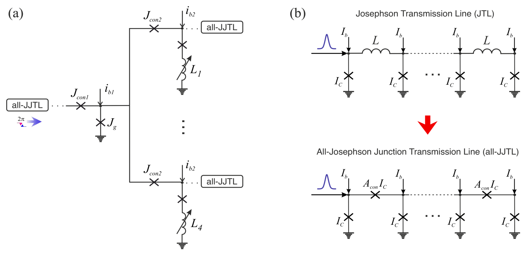
Figure 2.
(a) Parameter map of (, ). Using inductance values for enabling/disabling pulse transmission from the yellow region will not disrupt the operational mode of the other lines; the blue region indicates operational failure. The junction parameters are: with , with , and each of the four junctions with . Bias currents: ; . The bias current is applied to the common node and splits between and the four output branches. According to our simulations, starts to generate spontaneously only when , so at the junction remains stably superconducting with a comfortable static margin. A five-pointed star marks the point , which exhibits the largest separation between the blocking and transmitting inductance values while remaining slightly inside the boundary of the operational region, thereby providing a safe margin for practical implementation. (b) Orange: parameter map of valid (, ) for . Red: parameter map of valid (, ) for . An increase in the critical current of the connecting junctions leads to a narrowing of the operational parameter region.
Figure 2.
(a) Parameter map of (, ). Using inductance values for enabling/disabling pulse transmission from the yellow region will not disrupt the operational mode of the other lines; the blue region indicates operational failure. The junction parameters are: with , with , and each of the four junctions with . Bias currents: ; . The bias current is applied to the common node and splits between and the four output branches. According to our simulations, starts to generate spontaneously only when , so at the junction remains stably superconducting with a comfortable static margin. A five-pointed star marks the point , which exhibits the largest separation between the blocking and transmitting inductance values while remaining slightly inside the boundary of the operational region, thereby providing a safe margin for practical implementation. (b) Orange: parameter map of valid (, ) for . Red: parameter map of valid (, ) for . An increase in the critical current of the connecting junctions leads to a narrowing of the operational parameter region.
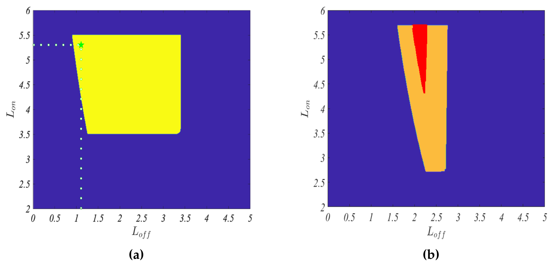
Figure 4.
Circuit diagram of a cell with controlled kinetic inductance for switching the circuit’s operation mode between XOR and OR logic gates. : . : . : . , .
Figure 4.
Circuit diagram of a cell with controlled kinetic inductance for switching the circuit’s operation mode between XOR and OR logic gates. : . : . : . , .
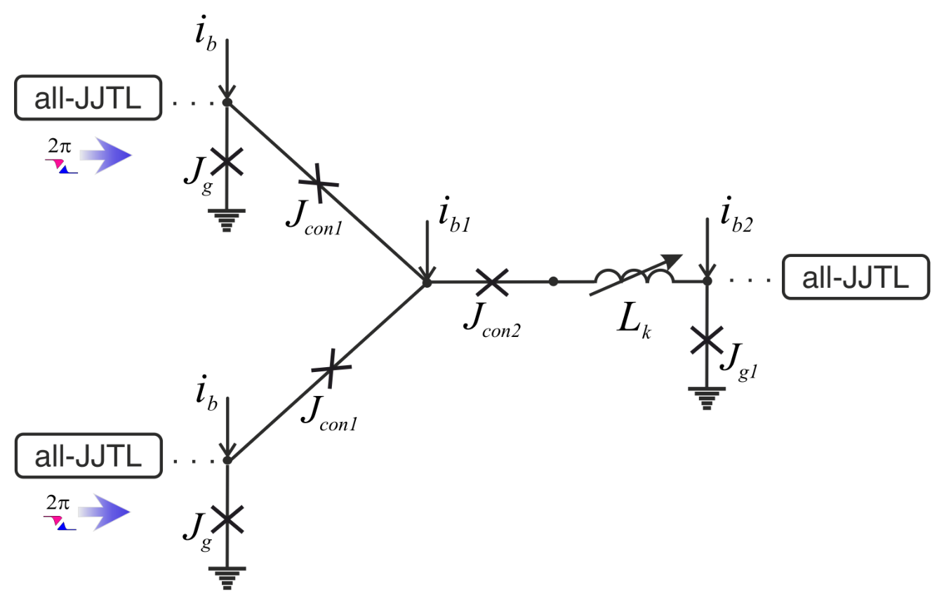
Figure 5.
Extended XOR cell with two tunable kinetic inductances, reconfigurable to realise the asymmetric functions and, by symmetry, . : . : . : . , .
Figure 5.
Extended XOR cell with two tunable kinetic inductances, reconfigurable to realise the asymmetric functions and, by symmetry, . : . : . : . , .
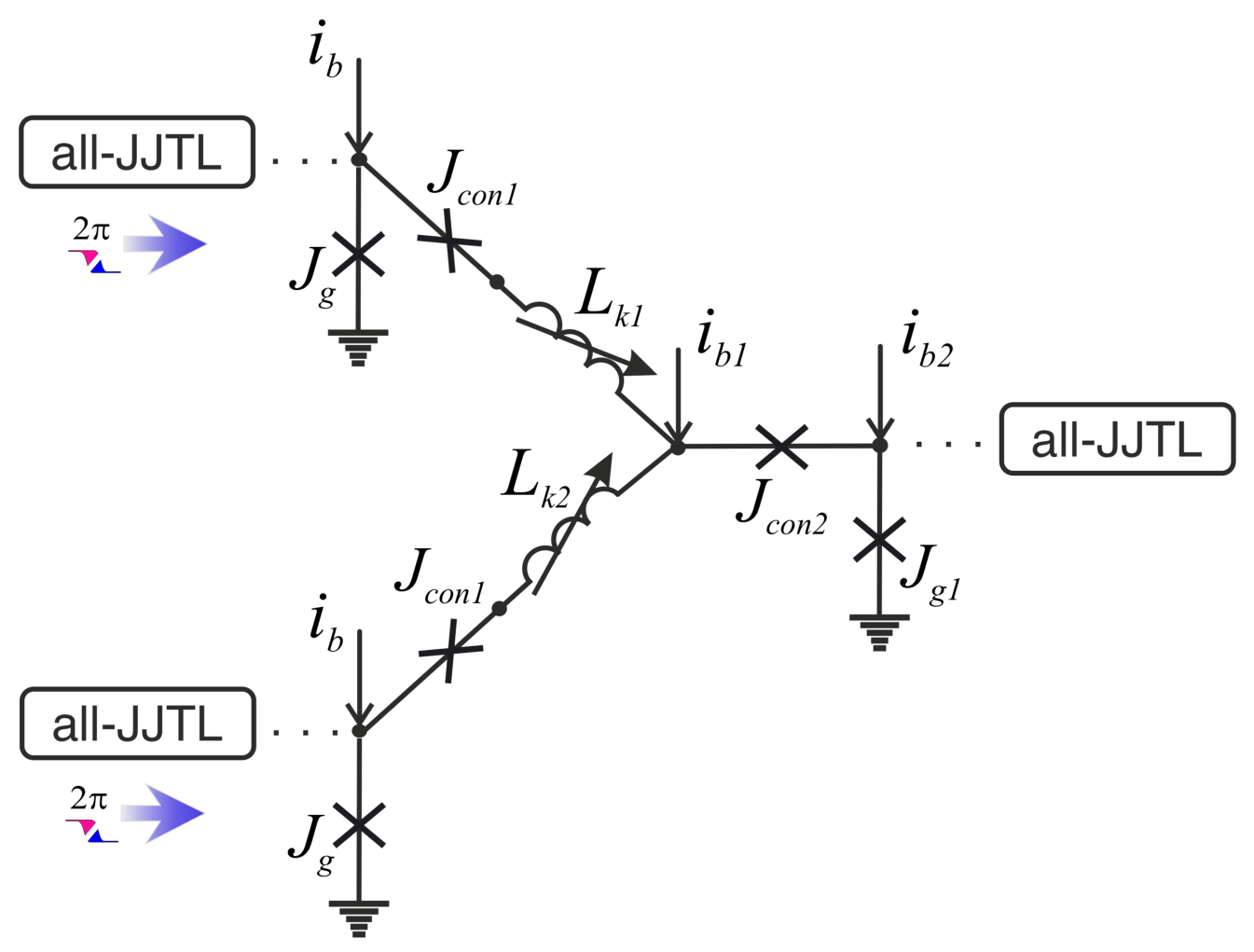
Figure 7.
Model of a superconducting bio-inspired neuron’s soma from [31]. Conventional circuit symbols for inductors, with red arrows drawn on them, denote kinetic inductance element.
Figure 7.
Model of a superconducting bio-inspired neuron’s soma from [31]. Conventional circuit symbols for inductors, with red arrows drawn on them, denote kinetic inductance element.
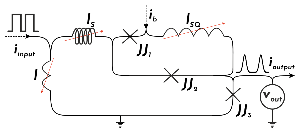
Figure 8.
Parameter domain of the superconducting bio-inspired neuron in the l– inductance plane. The labelled regions correspond to regular mode (RM), steady-state mode (SSM), bursting mode (BM), and non-biological mode (NBM). The fixed parameters are , , Josephson damping parameters (in [31] they were designated by ), and ( used as normalized critical current).
Figure 8.
Parameter domain of the superconducting bio-inspired neuron in the l– inductance plane. The labelled regions correspond to regular mode (RM), steady-state mode (SSM), bursting mode (BM), and non-biological mode (NBM). The fixed parameters are , , Josephson damping parameters (in [31] they were designated by ), and ( used as normalized critical current).
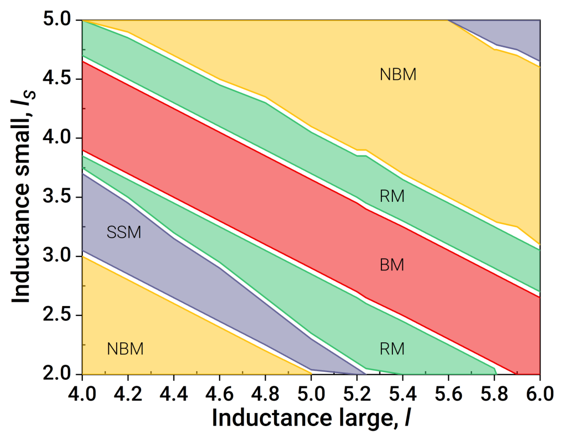
Figure 9.
Representative output-voltage traces of the superconducting bio-inspired neuron in different operating regimes: (a) regular mode, (b) bursting mode, (c) steady-state mode, and (d) non-biological mode.
Figure 9.
Representative output-voltage traces of the superconducting bio-inspired neuron in different operating regimes: (a) regular mode, (b) bursting mode, (c) steady-state mode, and (d) non-biological mode.
Disclaimer/Publisher’s Note: The statements, opinions and data contained in all publications are solely those of the individual author(s) and contributor(s) and not of MDPI and/or the editor(s). MDPI and/or the editor(s) disclaim responsibility for any injury to people or property resulting from any ideas, methods, instructions or products referred to in the content. |
© 2026 by the authors. Licensee MDPI, Basel, Switzerland. This article is an open access article distributed under the terms and conditions of the Creative Commons Attribution (CC BY) license (http://creativecommons.org/licenses/by/4.0/).
Copyright: This open access article is published under a Creative Commons CC BY 4.0 license, which permit the free download, distribution, and reuse, provided that the author and preprint are cited in any reuse.


