
Submitted:
23 May 2026
Posted:
25 May 2026
You are already at the latest version
Abstract
A compact rectangular microstrip patch antenna with enhanced impedance bandwidth is proposed for vehicular V2X applications operating at the 5.9 GHz ITS band. The design employs a single edge-notch slot to improve impedance matching and broaden the operational bandwidth. Full-wave electromagnetic simulations are performed using MATLAB Antenna Toolbox, enabling analysis of main antenna parameters including surface current distributions. Simulation results demonstrate that the slot excites an additional resonance that merges with the fundamental mode, increasing bandwidth from 240 MHz to approximately 500 MHz for VSWR < 2, fully covering the 5.85–5.925 GHz V2X band. Experimental measurements of VSWR show a bandwidth of approximately 490 MHz around the 5.9 GHz center frequency. Calculated peak gain (~8.3 dBi) and front-to-back ratio (~18.5 dB) are preserved. A parametric study of ground plane dimensions reveals the evolution of back-radiation patterns due to edge diffraction.
Keywords:
Microstrip patch antenna
; V2X communications
; bandwidth enhancement
; edge-notch slot
; MATLAB Antenna Toolbox
1. Introduction
Microstrip patch antennas are widely used in vehicular Vehicle-to-Everything (V2X) communication systems operating in the 5.9 GHz Intelligent Transportation Systems (ITS) band due to their low profile, mechanical robustness, and ease of integration into automotive platforms [1,2,3]. These properties make them suitable for rooftop installations and planar MIMO configurations in modern vehicles [1,4,11].
A major limitation of conventional microstrip patch antennas is their inherently narrow impedance bandwidth, typically ranging from 2% to 5% [5]. However, V2X systems require reliable operation over the 5.85–5.925 GHz band, which imposes strict bandwidth requirements under varying environmental and manufacturing conditions [2,3]. Increasing substrate thickness is a common approach to enhance bandwidth, but it may lead to higher cost and the excitation of surface waves that degrade radiation performance [6]. Various techniques have been proposed to increase bandwidth, including stacked patches, parasitic elements, and defected ground structures [6,7,8,9]. Among these methods, slot loading is particularly attractive due to its ability to introduce additional resonant modes without increasing antenna size or complexity [7,8]. However, many reported designs employ multiple slots or multilayer configurations, which complicate fabrication and integration [9,10]. The introduced slot in the proposed antenna modifies the surface current distribution and generates an additional resonance close to the fundamental TM₁₀ mode, resulting in significant bandwidth enhancement. This work employs MATLAB Antenna Toolbox simulation techniques [12–17] to analyze the proposed antenna with a single edge-notch slot for V2X applications.
2. Antenna Design
We performed a comparative analysis using two antennas simulated with MATLAB's Antenna Toolbox. The first antenna is used as a reference patch without slot. Both the reference and proposed antennas use Rogers RT/duroid 5880 substrate (εᵣ = 2.2, h = 1.57 mm) and a 50 × 50 mm finite ground plane. The antennas are fed by a coaxial probe. Dimensions of the probe were optimized for resonance near 5.9 GHz.

Table 1.
Dimensions of the Patch Antennas in mm.
| Parameter | Reference Patch | Slot Patch |
|---|---|---|
| Patch length (Lx) | 15.7 | 17.4 |
| Patch width (Wy) | 20.1 | 32.0 |
| Feed offset (from center) | 3.6 | 6.0 |
| Ground plane | 50x50 | 50x50 |
| Notch depth(a) | --- | 2.4 |
| Notch width (b) | --- | 18 |
Coaxial feeding method is adopted for these antennas. The inner conductor of the SMA connector with inner diameter equal 0.5 mm is connected to the patch, and the outer conductor is mated with the ground plane.
3. Reference Antenna
In this section simulation results for VSWR, Smith Chart, and gain of the reference antenna are presented. As shown in Figure 1 (left), the antenna has a simple patch geometry without a slot and operates in the 5.85–5.925 GHz V2X frequency band.
Current Distribution of the Reference Patch Antenna
Figure 2 (a) illustrates the surface current distribution (A/m) across the patch and the finite ground plane. The high current concentration at the edges of the patch and near the feed point confirms the excitation of the fundamental resonant mode. Notably, the current density tapers off significantly toward the edges of the 50x50 mm ground plane, which validates the chosen dimensions for minimizing edge diffraction and surface wave wrap-around.
VSWR and Smith Chart
As seen in Figure 3 (a), the reference antenna exhibits a bandwidth of approximately 240 MHz with a resonant frequency of approximately 5.9 GHz. This value is determined for the frequency range of 5.85 GHz to 6.09 GHz, where VSWR remains below 2.
Radiation Patterns and Gain Analysis
The left image of Figure 4(a) presents the normalized radiation patterns of the reference antenna in the E-plane (φ = 0°) and H-plane (φ = 90°), both normalized to the maximum directivity in the boresight direction (Z-axis). The patterns represent the total directivity, computed from the combined orthogonal electric field components as illustrated in the inset of Figure 4
The right image of Figure 4(a) presents the 3D total directivity pattern (dBi), showing a well-defined hemispherical beam centered on the boresight (Z-axis).
According to simulations, the maximum gain in the Z-direction is approximately G = 8.3 dBi. The relationship between the maximum gain (G) and the directivity (D) is governed by the radiation efficiency (η) as: G = η · D. The Rogers RT/duroid 5880 substrate features an exceptionally low loss tangent (tan δ = 0.0009), ensuring high radiation efficiency typically exceeding 90% (η > 0.9). Using this efficiency value, the calculated directivity (D) is approximately 9.1 dBi.
Back Radiation Level
Simulation results demonstrate that the antenna exhibits a suppressed back radiation level of -21.55 dB in E-plane and of -16.72 dB in H-plane. This result represents the effective relative side-lobe level (SLL) in the backward hemisphere compared to the main radiation beam. According to the calculations by the 3D pattern average back radiation is -9.97 dBi and Front-to-Back Ratio is equal 18.19 dB, which agrees well with the results obtained from the E- and H-plane cuts.
4. Antenna Parameters with Edge-Notch Slot
This proposed antenna is constructed on the substrate board with the same parameters as a reference patch. The right image in Figure 1 shows proposed geometry design. Slot dimensions were optimized to achieve minimum VSWR and maximum bandwidth.
Current Distribution of the Edge-Notch Slot Patch Antenna
The current distribution (Figure 2(b)) is strongly perturbed by the presence of the slot.
A pronounced current concentration appears around the feed region and along the slot edges, indicating that the slot introduces additional current paths and locally enhances the surface current density. The current is no longer uniformly distributed over the patch; instead, it is distorted and partially redirected around the slot, leading to a more complex current pattern. In contrast, the conventional patch without a slot exhibits a smoother and more symmetric current distribution (Figure 2(a)), primarily concentrated along the radiating edges. The absence of discontinuities allows the current to flow more uniformly across the patch surface. The introduction of the slot therefore increases current localization, modifies current paths, and introduces asymmetry, which affect the radiation characteristics, including bandwidth and back radiation behavior.
VSWR and Smith Chart for the Patch with Increased Bandwidth
VSWR plot (Figure 3 (b)) shows a wide impedance bandwidth where VSWR remains below
2 from 5.655 GHz to 6.159 GHz, corresponding to a bandwidth of approximately 503.8 MHz. The minimum VSWR occurs near the center frequency around 5.9 GHz, indicating good impedance matching. The corresponding Smith chart confirms this behavior: the impedance trajectory forms a relatively compact loop around the center of the chart, remaining close to the matched condition over a broad frequency range. This indicates improved broadband matching due to the presence of the slot.
Radiation Patterns and Gain Analysis
The radiation patterns of the proposed slotted antenna with 50 × 50 mm ground plane (Figure 4 (b)) show a well-defined broadside main lobe with reasonable symmetry in both the E- and H-planes. The 3D pattern confirms an overall hemispherical shape. Compared to the reference antenna, the slotted design maintains similar forward radiation characteristics, while the averaged back radiation levels are −19.27 dB (E-plane) and −17.84 dB (H-plane), resulting in a combined front-to-back ratio of approximately 18.4 dB.
Figure 5 shows normalized radiation patterns of the antenna with ground plane of 150x150 mm (a) and 250x250 mm(b). All images of Figure 5 demonstrate a well-defined broadside main lobe. However, it can be observed that the back-radiation pattern undergoes a significant transformation as the linear ground size increases from one wavelength (Figure 4) to 5 wavelength (Figure 5). For a small ground plane (50 mm), the pattern remains relatively smooth. However, as the dimensions increase, the back-lobe region exhibits rapid spatial oscillations, forming a dense "comb" of lobes, whose periodicity decreases with increasing ground plane electrical size. This phenomenon is attributed to the edge diffraction of surface currents at the boundaries of the finite ground plane.
Table 2 presents the simulated radiation characteristics of the proposed antenna across various ground plane dimensions. The results indicate that as the ground size increases from 1.02 λ to 5.08 λ, the antenna's Back-Lobe Count undergoes significant changes. The table highlights a clear correlation between the electrical size of the ground plane and the density of back-radiation oscillations, which evolve from a simple two-lobed structure into a dense multi-lobed pattern.
5. Experimental Results
The VSWR of the fabricated antenna prototype was experimentally measured using an Agilent network analyzer. The comparison between simulated and measured VSWR, shown in Figure 6(b), demonstrates good agreement, confirming the validity of the design. The measured impedance bandwidth, defined for VSWR ≤ 2, is approximately 490 MHz, covering the frequency range from 5.54 GHz to 6.03 GHz, centered around 5.9 GHz. Experimental validation of the radiation characteristics (E- and H-plane patterns) will be addressed in future work.
6. Conclusions
This article has presented a bandwidth enhancement technique for a 5.9 GHz V2X microstrip patch antenna through the introduction of a single edge-notch slot into the patch metallization. The proposed design was evaluated against a reference patch antenna through full-wave electromagnetic simulation using MATLAB Antenna Toolbox.
The introduction of the slot modifies the surface current distribution, redirecting current paths around the slot edges and introducing an additional resonance in close proximity to the fundamental TM₁₀ mode. The merging of these two resonances results in increase of the impedance bandwidth from 240 MHz for the reference patch to approximately 500 MHz for the slotted design. Radiation performance is well preserved: the peak gain of ~8.3 dBi and the front-to-back ratio of 18.5 dB are maintained at a level comparable to the reference antenna, confirming that the slot loading does not degrade the directional properties essential for automotive rooftop installation. A parametric study of the ground plane size from 1λ to 5λ reveals that the back-radiation pattern undergoes significant transformation with increasing electrical size. While the averaged front-to-back ratio remains above 17.7 dB across all studied configurations, the back-lobe region develops a dense oscillatory structure caused by edge diffraction of surface currents.
The proposed single-slot modification offers a practical and low-cost solution for V2X antenna design, requiring no additional substrate layers, no increased board thickness, and no complex geometry, making it directly suitable for integration into automotive antennas.
References
- Katare, K. K.; Yousaf, I. M.; Lau, B. K. Challenges and solutions for antennas in vehicle-to-everything services. IEEE Commun. Mag. 2021, vol. 60(no. 1), 52–58. [Google Scholar] [CrossRef]
- Intelligent Transport Systems (ITS); Access layer specification for ITS operating in the 5 GHz band. ETSI EN 302 663 V2.1.1; ETSI. 2019.
- IEEE Std 802.11-2020; IEEE Standard for Information Technology— Wireless LAN Medium Access Control and Physical Layer Specifications. 2020.
- Rabinovich, V.; Alexandrov, N.; Alkhateeb, B. Automotive Antenna Design and Applications; CRC Press: Boca Raton, FL, USA, 2010. [Google Scholar]
- Krishna, N. R. P. S.; Shirish, H.; Isfahani, A. M. H.; Manisha, K. Design of dual rectangular slotted microstrip patch antenna for S-band. Proc. 4th Int. Conf. Emerging Technol. (INCET), May 2023; pp. 1–6. [Google Scholar]
- Wang, L.; Deng, D.; Yan, B.; Luo, Z.; Feng, L.; Zheng, H. Quad-band microstrip antenna with only one slot on the edge. Proc. 11th Int. Symp. Antennas Propag. EM Theory (ISAPE), Guilin, China, Oct. 2016; pp. 295–298. [Google Scholar]
- Fan, S. T.; Yin, Y. Z.; Lee, B.; Hu, W.; Yang, X. Bandwidth enhancement of a printed slot antenna with a pair of parasitic patches. IEEE Antennas Wirel. Propag. Lett. 2012, vol. 11, 1230–1233. [Google Scholar] [CrossRef]
- Harideepak, V. Triple band crown shaped slotted microstrip patch antenna. Proc. IEEE Wireless Antenna Microwave Symp. (WAMS), Chennai, India, Jun. 2025; pp. 1–4. [Google Scholar]
- Ourahou, O.; Belhrach, H.; Ghammaz, A. A new miniaturized multi-band transparent antenna for V2X communication. IMT Web Conf., 2024. [Google Scholar]
- Chang, Y.; Gao, X.; Wang, T.; Zhang, N.; Ding, S.; Ma, S. Wideband enhanced microstrip patch antenna for C-band application. Proc. IEEE 7th Int. Conf. Civil Aviation Safety Inf. Technol. (ICCASIT), Yinchuan, China, Oct. 2025; pp. 369–373. [Google Scholar]
- Rabinovich, V.; Alexandrov, N. Antenna Arrays and Automotive Applications; Springer: New York, NY, USA, 2013. [Google Scholar]
- Shaw, M.; Sarkar, P. Determination of principal resonant frequency and optimum probe position of microstrip antenna using MATLAB. Proc. 9th Int. Conf. Electron., Mater. Eng. Nano-Technol. (IEMENTech), 2026; pp. 1–6. [Google Scholar]
- Ilyanova, D. S.; Nazarov, I. V.; Yelizarov, A. A.; Zakirova, E. A.; Khandelwal, M. K. Simulation of a reconfigurable phased antenna array with directional beam control. Proc. Int. Conf. Signal Synchronization, Generating Process. Telecommun. (SYNCHROINFO), Moscow, Russia, 2025; pp. 1–5. [Google Scholar]
- Narmatha, D.; Abinaya, K. Simulation-based antenna design using MATLAB App Designer. Res. Rev. Electron. Commun. Eng. 2025, vol. 2(no. 3), 11–21. [Google Scholar]
- Manoj, B.; Rodriguez, S. Optimization of microstrip patch antenna dimensions using genetic algorithm. Proc. 7th Int. Conf. Adv. Comput. Commun. Syst. (ICACCS), Kochi, India, 2021; pp. 598–603. [Google Scholar]
- Vavrečková, K.; Olivová, J.; Richterová, M.; Popela, M. Patch antenna for monitoring UWB signals. Proc. Int. Conf. Military Technol. (ICMT), Brno, Czech Republic, 2021; pp. 1–5. [Google Scholar]
- Yadav, S.; Patel, P. Constrained parameter analysis of microstrip antenna. Proc. Int. Conf. Soft-Computing Netw. Security (ICSNS), Coimbatore, India, 2015; pp. 1–4. [Google Scholar]
Figure 1.
Geometry of the reference and proposed patch antennas: top view and side view.
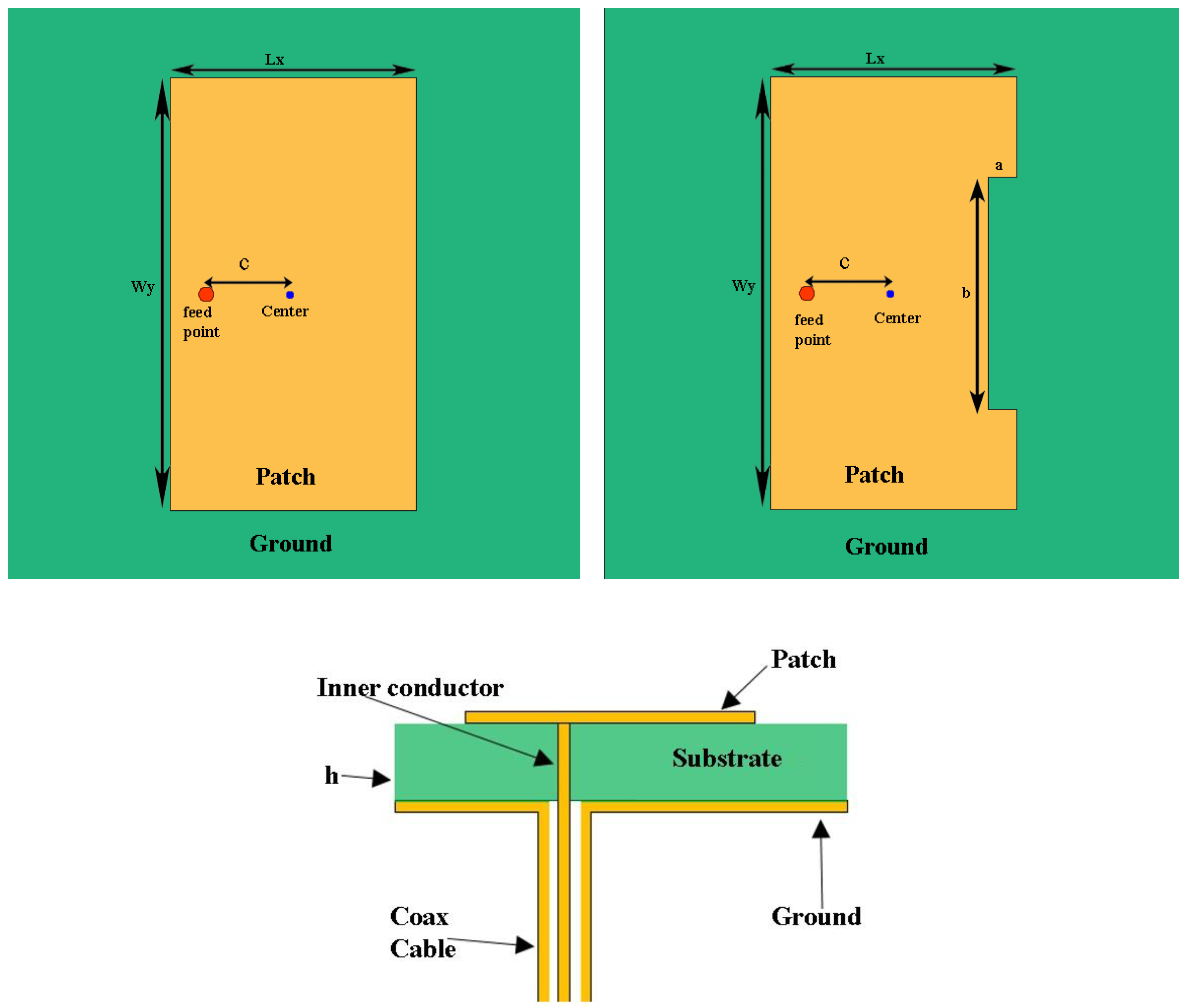
Figure 2.
Surface current distribution at 5.9 GHz. a) Reference Antenna; b) Proposed Antenna.
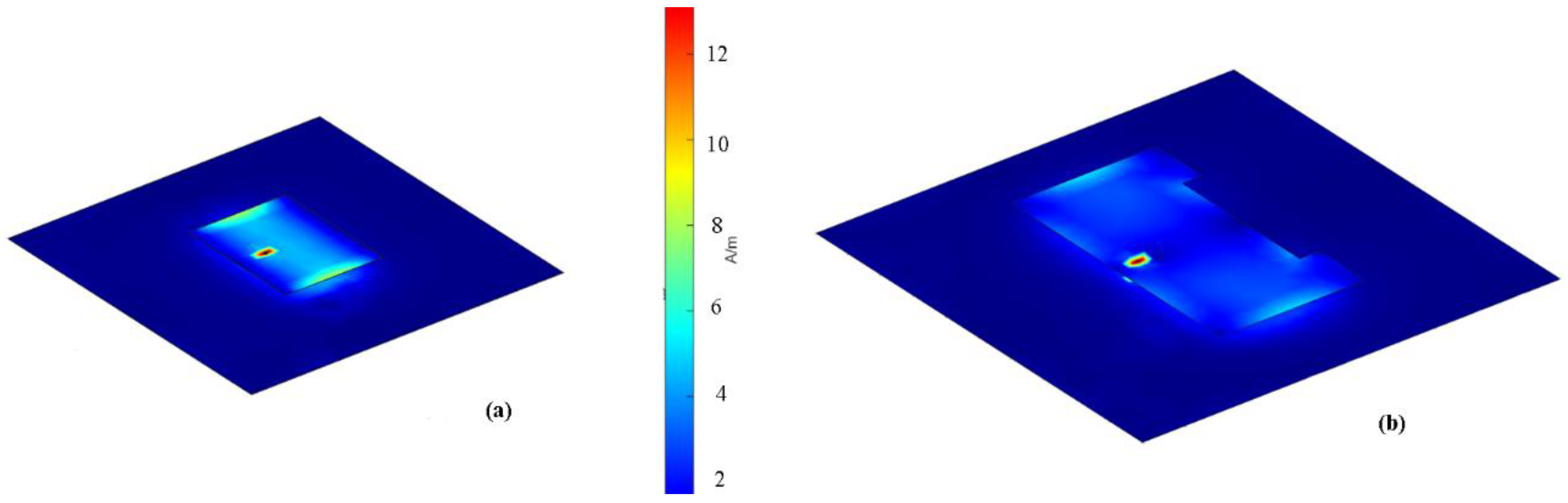
Figure 3.
VSWR and Smith chart: (a) Reference Antenna; (b) Proposed Antenna.
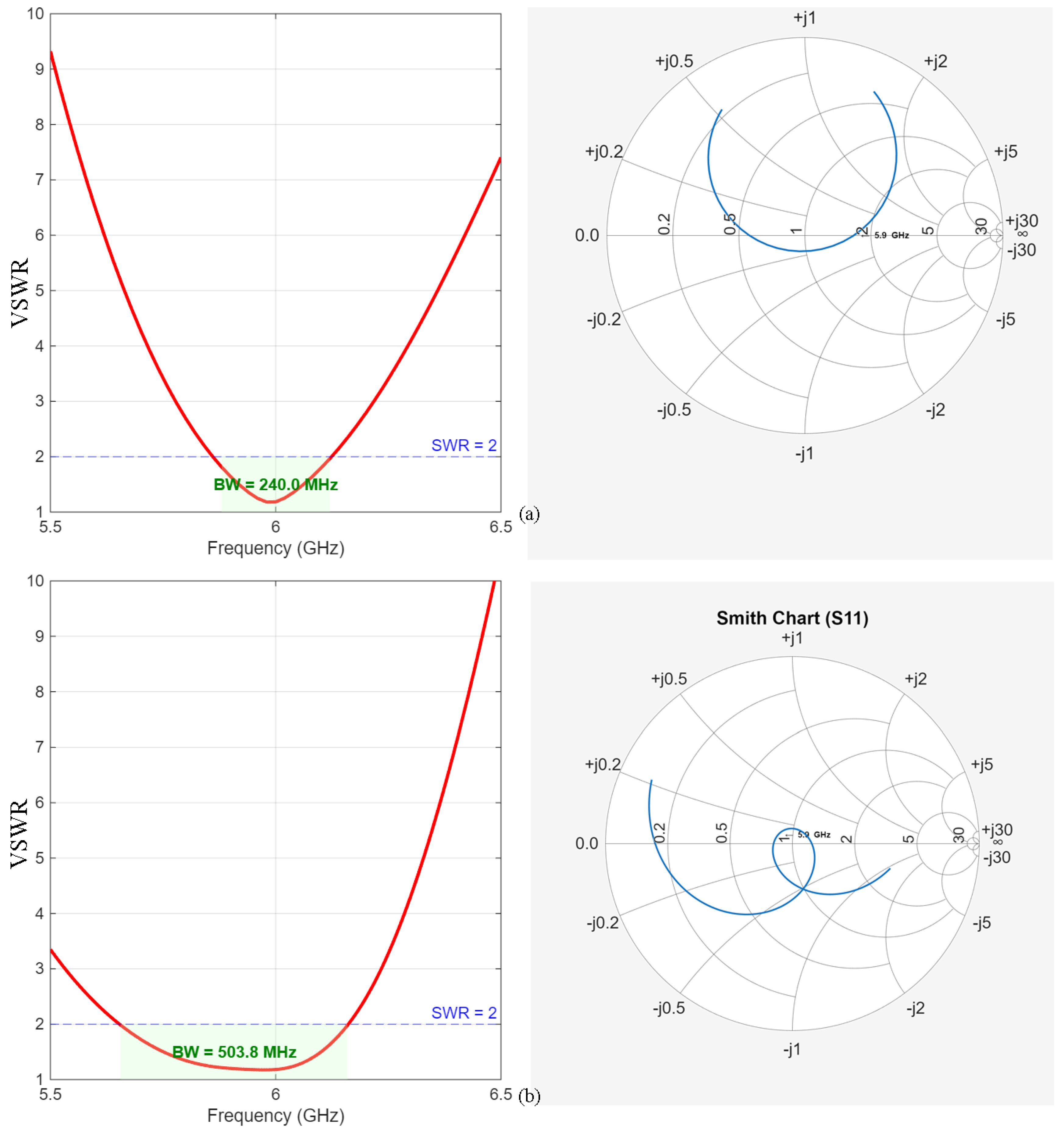
Figure 4.
2D (E- and H-plane) and 3D radiation patterns at 5.9 GHz. (a) Reference Antenna; (b) Proposed Antenna.
Figure 4.
2D (E- and H-plane) and 3D radiation patterns at 5.9 GHz. (a) Reference Antenna; (b) Proposed Antenna.
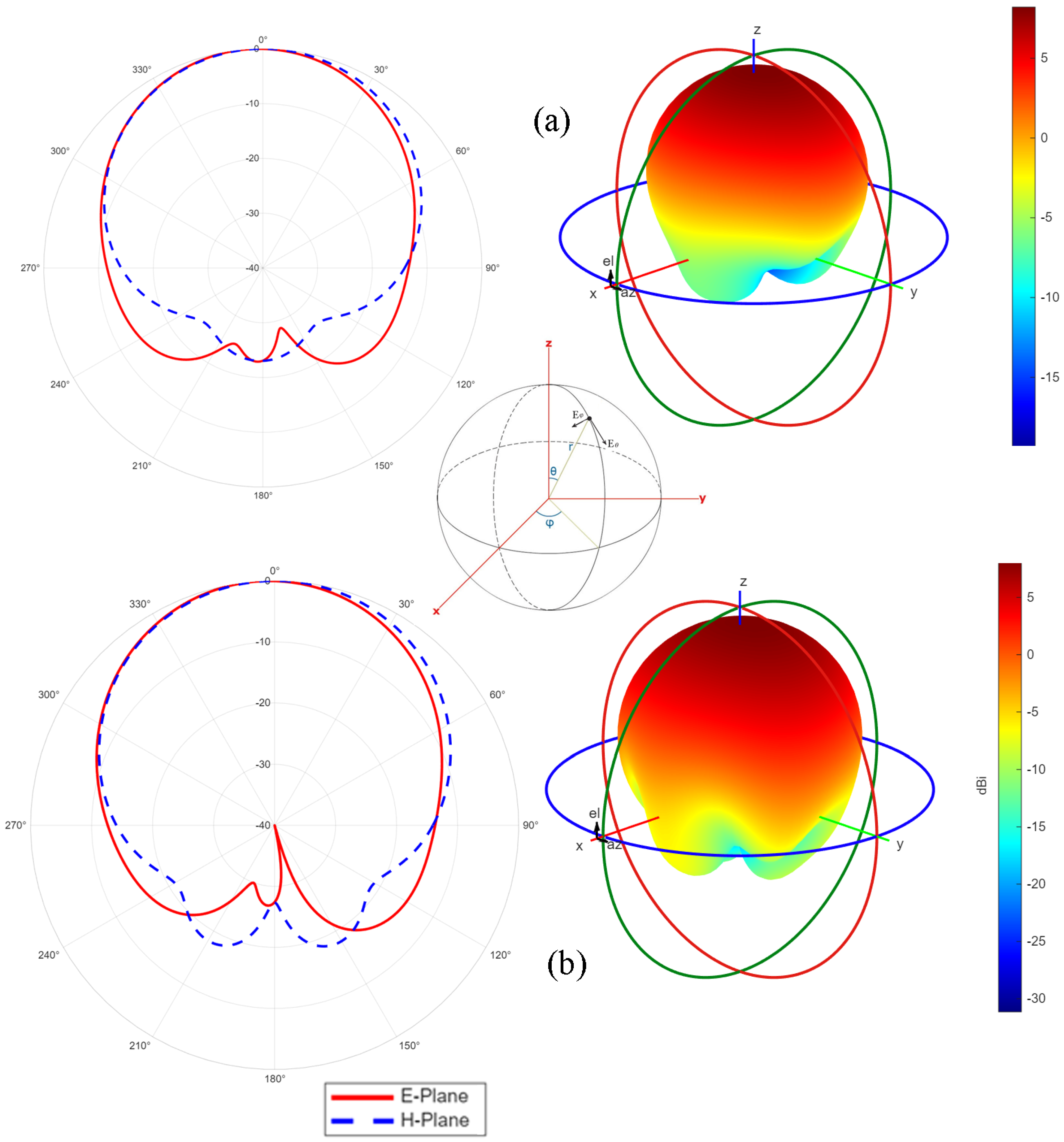
Figure 5.
Normalized E-plane (solid line) and H-plane (dashed line) radiation patterns of the proposed antenna at 5.9 GHz for (a) 150 × 150 mm and (b) 250 × 250 mm ground plane.
Figure 5.
Normalized E-plane (solid line) and H-plane (dashed line) radiation patterns of the proposed antenna at 5.9 GHz for (a) 150 × 150 mm and (b) 250 × 250 mm ground plane.
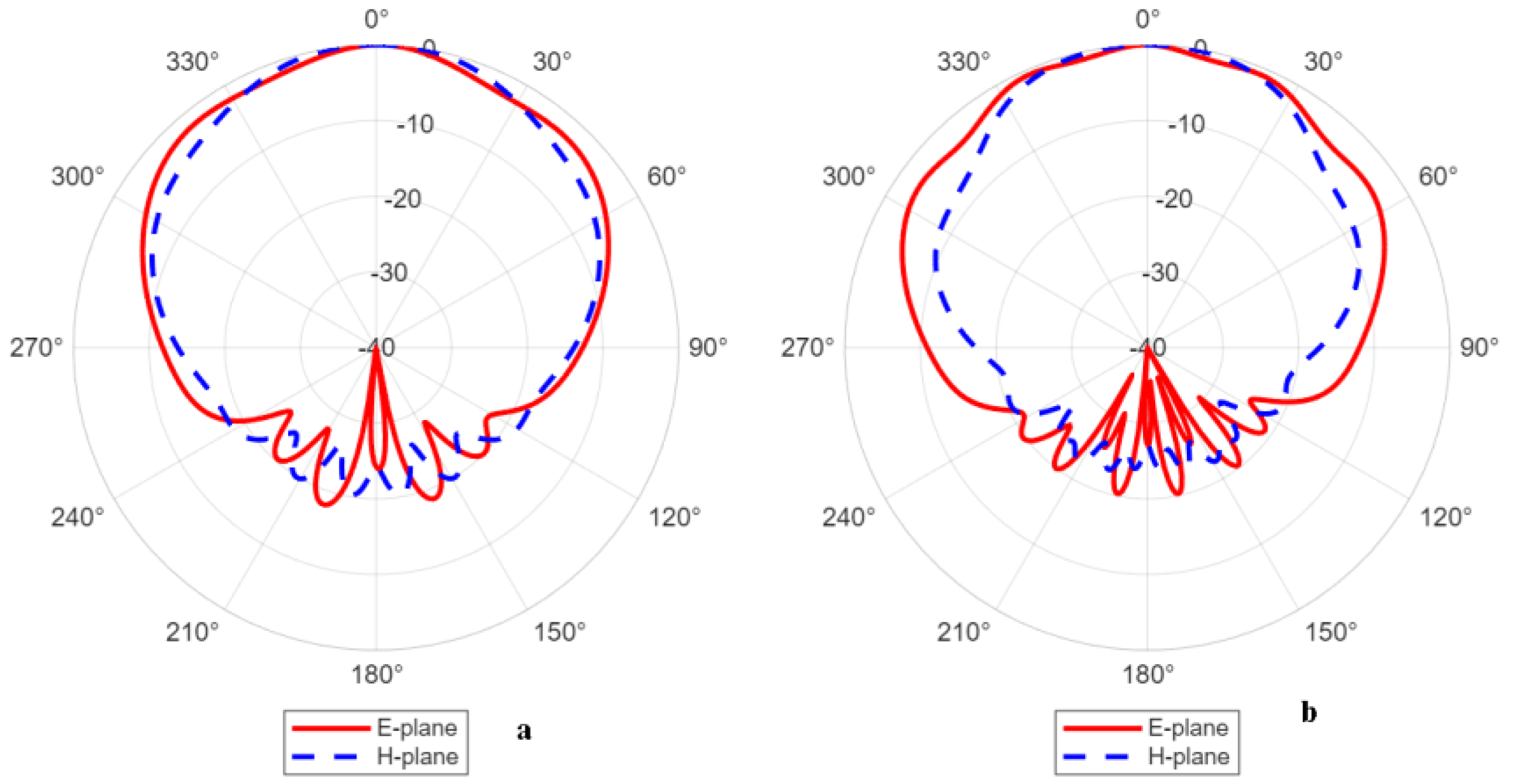
Figure 6.
(a) Antenna Prototype (b) VSWR: simulation (solid) and measurement.
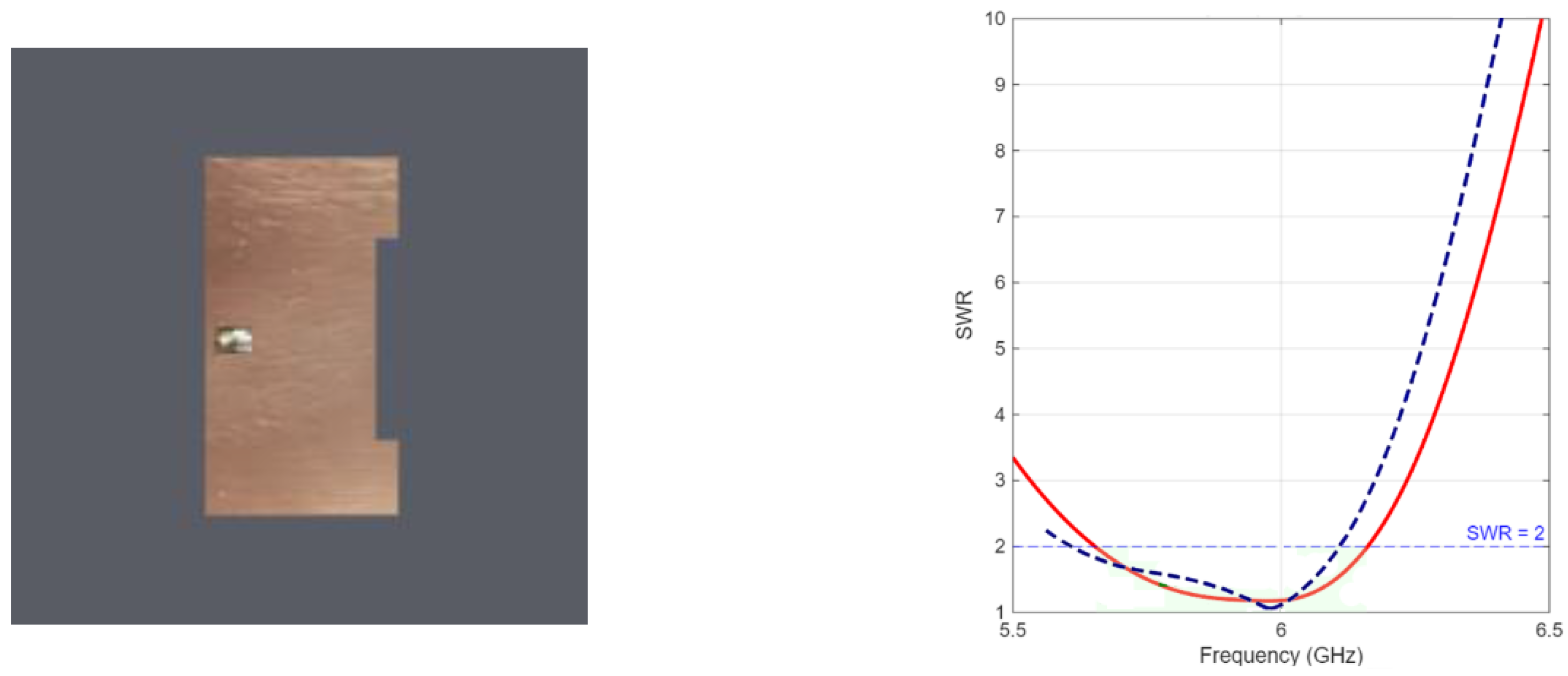
Table 2.
Front to Average Back Radiation for Antenna with Different Ground Size.
| Ground Size | λ/Lgnd | F/B (dB) 2D | F/B (dB) 3D | Peak Gain | Back-Lobe Count |
|---|---|---|---|---|---|
| 50 | 1.02 λ | 18.5 | 18.68 | 8.3 dBi | ~ 2 |
| 100 | 2.03 λ | 17.76 | 18.10 | 7.48 dBi | ~4 |
| 150 | 3.05 λ | 19.43 | 19.59 | 8.05 dBi | ~6 |
| 200 | 4.06 λ | 18.48 | 19.33 | 7.64 dBi | ~8 |
| 250 | 5.08 λ | 21.14 | 21.55 | 8.39 dBi | ~10 |
Notice: F/B means ratio between the maximum gain in the Z-direction and the average radiation in the backward hemisphere.
Disclaimer/Publisher’s Note: The statements, opinions and data contained in all publications are solely those of the individual author(s) and contributor(s) and not of MDPI and/or the editor(s). MDPI and/or the editor(s) disclaim responsibility for any injury to people or property resulting from any ideas, methods, instructions or products referred to in the content. |
© 2026 by the authors. Licensee MDPI, Basel, Switzerland. This article is an open access article distributed under the terms and conditions of the Creative Commons Attribution (CC BY) license (http://creativecommons.org/licenses/by/4.0/).
Copyright: This open access article is published under a Creative Commons CC BY 4.0 license, which permit the free download, distribution, and reuse, provided that the author and preprint are cited in any reuse.


