
Submitted:
21 May 2026
Posted:
22 May 2026
You are already at the latest version
Abstract
Lithium niobate on insulator (LNOI) has emerged as a promising platform for compact, low-loss phase modulators. The extant LNOI studies evaluate device performance almost exclusively through the Pockels effect, treating piezoelectric-photoelastic strain and thermo-optic drift as decoupled channels. Crucially, both mechanisms directly perturb the phase bias of a fiber-optic gyroscope (FOG), rendering them indispensable in sensing-oriented design. This work establishes a unified multiphysics model of an X-cut TFLN ridge phase modulator that self-consistently couples the electro-optic, piezoelectric-photoelastic, thermo-optic, and pyroelectric channels. The contributions of the four mechanisms are quantitatively decomposed under realistic FOG operating conditions, and the slab thickness, ridge top width, and electrode gap are systematically optimized to balance modulation efficiency against environmental robustness. The co-optimization of the ridge geometry and electrode gap design maintains the EO overlap factor near 0.55 while reducing the half-wave voltage requirement. This results in a half-wave voltage length of VπL = 1.65 V·cm at a 4.4 μm electrode gap. The optimal gap shifts only marginally to 4.2 μm at 85℃, with VπL increasing modestly from 1.65 to 1.93 V·cm (push-pull single-pass) across 25~85 °C, attributable to the intrinsic γ33 change of LiNbO3. Furthermore, a substrate temperature rise of 60 K under operating bias induces a mode field weighted thermal residual of approximately −3.1 × 10⁻⁵ (equivalent to −6.3 × 10⁻⁶ in spatial-average form). This thermal residual corresponds to approximately 27% of the Pockels modulation depth at an applied voltage of 5 V. The present study demonstrates that the DC-coupled operation of TFLN sensor-grade modulators is viable across the full FOG temperature range without active thermal compensation. The results of the study provide quantitative design guidelines for high-performance, environmentally stable TFLN phase modulators in compact FOG systems.
Keywords:
lithium niobate on insulator
; phase modulator
; multiphysics coupling
; fiber-optic gyroscope
1. Introduction
Fiber-optic gyroscopes (FOGs) have been extensively utilized in inertial navigation, attitude control, and precision measurement due to their inherent advantages, including the absence of moving components, rapid initialization, high accuracy, and exceptional reliability [1]. The advent of unmanned systems, intelligent transportation, and miniaturized industrial sensing has driven a paradigm shift in inertial device development. These devices are undergoing a transition towards smaller form factors, reduced power consumption, and heightened levels of integration. For FOGs, this trend translates into a stringent set of requirements. In addition to a more compact footprint and reduced drive power, sensor-grade operation demands low bias drift, high long-term stability, and accurate scale factors under realistic environmental conditions [2,3].
The phase modulator is the core optoelectronic component that closes the FOG feedback loop, simultaneously providing beam splitting/combining, polarization filtering, and phase modulation [4,5]. Its half-wave voltage, modulation linearity, and environmental stability translate directly into the bias stability, scale-factor error, and long-term accuracy of the gyroscope. An ideal FOG-grade phase modulator therefore combines a low drive voltage, a compact footprint, a linear phase response, and strong robustness against thermal and mechanical perturbations. Conventional bulk lithium niobate (LN) modulators fabricated by titanium in-diffusion or annealed proton exchange offer mature processing and excellent electro-optic performance [6], but their large size, relatively high drive voltage, and long-term bias drift make it increasingly difficult to satisfy the integration and stability demands of next-generation miniaturized FOGs. To address these limitations, integrated phase modulators have been realized on silicon, indium phosphide (InP), and electro-optic polymer platforms [7]. Each of these platforms, however, exhibits intrinsic limitations for sensor-grade use: silicon modulators rely on the plasma-dispersion effect and are therefore susceptible to nonlinearity, free-carrier absorption, and temperature sensitivity [8]; InP modulators achieve compact integration but typically require active thermal stabilization for reliable operation [9]; and polymer modulators still suffer from insufficient long-term reliability [10]. Thin-film lithium niobate on insulator (TFLN), by contrast, combines a high refractive-index contrast, strong optical confinement, low propagation loss, and a highly linear Pockels response, making it one of the most promising platforms for high-performance integrated phase modulators, with demonstrated ad-vantages in low voltage and high-speed modulation [11,12,13,14,15,16].
Beyond the Pockels effect, lithium niobate also exhibits pronounced direct and converse piezoelectric coupling and a significant thermo-optic response: the modulating electric field induces mechanical strain [17] that perturbs the effective index through the photoelastic effect [18], while temperature variation drives a thermo-optic index drift together with pyroelectric phase bias fluctuations. Although bulk LN phase modulators have been studied extensively and supported by a mature device and packaging ecosystem [19]. However, the majority of prior work has focused on characterizing or compensating Vπ, bias drift, and residual intensity modulation, without establishing a unified multiphysics description of piezoelectric-photoelastic coupling and thermo-optic drift [20]. In high-precision sensing applications such as FOGs, however, the true phase response under simultaneous electrical drive [21], thermal load, and mechanical perturbation is directly tied to bias stability and long-term measurement accuracy. Several studies have examined the impact of temperature variation [22], mechanical vibration, or packaging stress on the output characteristics of bulk modulators [23], and others have addressed the influence of external perturbations on FOG bias stability; yet these analyses commonly treat thermal and stress effects as in-dependent external disturbances and do not systematically resolve the physical origin and relative weight of each contribution from the joint action of material constitutive behaviors, waveguide confinement, and device geometry [24,25]. The existing literature therefore captures that performance varies under perturbation but provides little quantitative insight into which coupling mechanisms dominate and how each con-tributes within a realistic device structure [26].
A further gap concerns TFLN itself. Almost all existing studies of TFLN modulators are oriented toward telecom applications, where the evaluation focuses on propagation loss, the half wave voltage length product VπL, and modulation bandwidth, leaving the multiphysics behaviors under FOG-relevant operating conditions largely unaddressed [27]. TFLN devices are not physically equivalent to their bulk counterparts from a multiphysics standpoint: thin-film LN is typically patterned into high-index-contrast ridge waveguides with stronger mode confinement and a smaller electrode-to-waveguide spacing, so that the electric-field, strain [28], and temperature distributions all couple more tightly to the guided-mode effective index [29]. This concentrated geometry is doubly consequential—it boosts electro-optic efficiency and lowers the drive voltage, but it may simultaneously amplify the influence of piezoelectrically induced strain and local thermal gradients on the phase response. Consequently, transferring empirical conclusions from bulk LN devices to TFLN under FOG operating conditions tends to misrepresent the actual physics, and a Pockels-only analysis is insufficient to meet the environmental-robustness and phase-stability requirements of FOG-grade design.
Motivated by these considerations, the present work targets FOG sensing applications and develops a multiphysics analysis framework for an X-cut LNOI ridge phase modulator that self-consistently couples the electro-optic, piezoelectric-photoelastic, thermo-optic, and pyroelectric channels. A finite-element implementation is used to quantitatively resolve the effective-index change and phase response of the device un-der realistic FOG operating conditions. Building on this framework, the slab thickness, ridge top width, and electrode gap are systematically optimized against the requirements of sensor-grade operation, with the aim of balancing modulation efficiency, fabrication feasibility, and environmental robustness. The results provide quantitative design guidelines and an optimization pathway for compact, low-voltage, high-stability TFLN phase modulators suited to medium- and high-precision FOG systems.
The main contributions of this work are summarized as follows:
- A multiphysics model of a TFLN ridge phase modulator is developed that couples electro-optic, piezoelectric-photoelastic, thermo-optic, and pyroelectric effects within a unified finite-element framework.
- The individual contributions of the EO, PE (V-synchronous and V-indepenent), and TO/pyroelectric mechanisms are quantitatively decomposed; the analysis reveals that V-independent thermal-elastic PE reaches unignorable ~27% of the Pockels modulation depth at ΔT = 60 K and that EO only analysis systematically underestimates the bias-stability budget required for sensor-grade operation.
- The influence of slab thickness, ridge top width, and electrode gap on the overlap factor and VπL is systematically investigated, yielding an optimized geometry with a push-pull VπL of 1.65 V·cm at a 4.4 μm electrode gap (25 °C) for sensor-grade operation, with the optimal geometry remaining stable across the 25~85 °C FOG operating range.
- The implications of the optimized design for FOG integration are discussed in terms of modulation efficiency, bias stability, and environmental robustness.
- A head-to-head comparison with competing phase-modulator platforms highlights the competitive advantages of TFLN for compact, stable, and low-power FOGs.
To the best of our knowledge, this is the first study that simultaneously couples all three channels and quantitatively decomposes their contributions in a FOG context.
2. Multiphysics Model for FOG-Oriented TFLN Modulators
2.1. Device Geometry
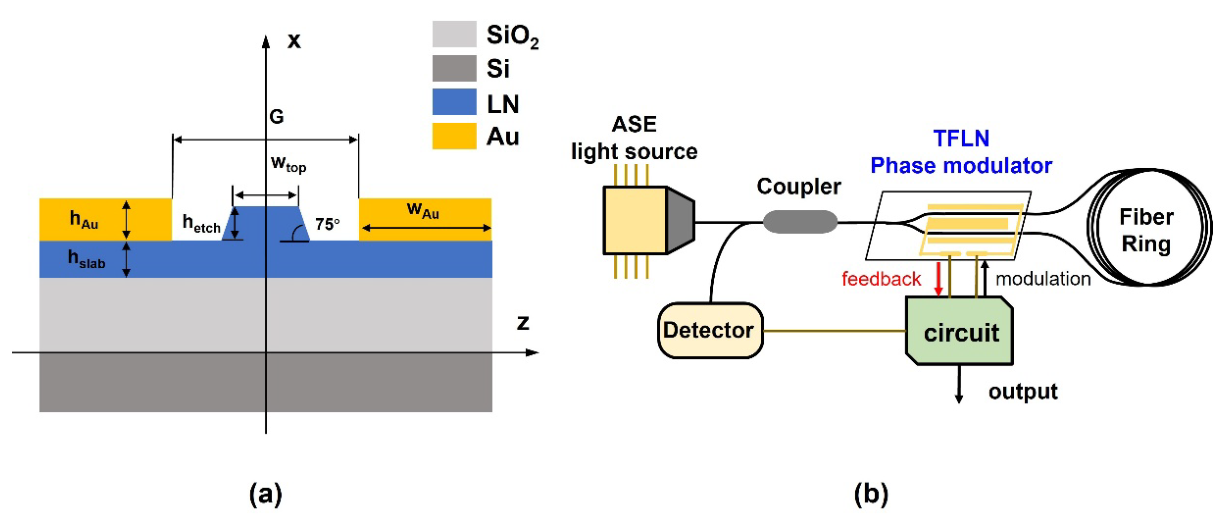
The proposed device is a ridge-type TFLN phase modulator designed for FOG applications. The waveguide is defined on an X-cut LNOI platform (thickness of wafer parameters from NANOLN) with light propagating along the Y-direction, so that the in-plane component of the applied electric field acts through the largest EO tensor element of LN. A coplanar electrode configuration generates the lateral modulation field across the ridge, and the ridge geometry is chosen to provide strong optical confinement while maintaining moderate fabrication complexity and good overlap between the guided mode and the applied field.
Three geometric parameters dominate the device behavior: the original TFLN slab thickness hslab= 100 nm, the ridge top width wtop = 1.3 μm, the etching angle is set to 75° based on manufacturing experience and the electrode gap g = 5 μm. As discussed later, these parameters jointly control the optical mode confinement, the electric-field distribution, the piezoelectric strain pattern, and the fraction of heat dissipated through the ridge. A parametric sweep of these three dimensions is therefore applied to identify a design that balances modulation performance, fabrication feasibility, and robustness against thermal and mechanical perturbations.
Figure 1.
(a) Cross section schematic of the TFLN ridge phase modulator for FOG applications, showing the ridge waveguide, slab layer, coplanar electrodes, and the coordinate system, x axis refer to LN c-axis. (b) System schematic of the reflective FOG incorporating a TFLN phase modulator.
Figure 1.
(a) Cross section schematic of the TFLN ridge phase modulator for FOG applications, showing the ridge waveguide, slab layer, coplanar electrodes, and the coordinate system, x axis refer to LN c-axis. (b) System schematic of the reflective FOG incorporating a TFLN phase modulator.
2.2. Material Parameters and Boundary Conditions
The optical, mechanical, piezoelectric, photoelastic, and thermal properties of each material layer are taken from established literature values and summarized in Table 1. For the electrostatic problem, the two electrodes are set to a prescribed voltage difference and the surrounding domains are treated as electrically neutral dielectrics. For the mechanical problem, the bottom surface is clamped to represent the substrate support. For the thermal problem, the bottom boundary is held at a prescribed temperature (used both to emulate substrate heat-sinking and to impose controlled temperature rises), while the remaining external boundaries are treated as thermally insulating unless otherwise stated. The fundamental quasi-TE mode is selected as the operating mode because of its strong overlap with the dominant γ33 element of the X-cut LN EO tensor.
For LiNbO3, the Pockels coefficients are γ33 = 30.9 pm/V and γ13 = 9.6 pm/V; the photoelastic constants (Weis & Gaylord, 1985 [17]) are p11 = −0.026, p12 = 0.090, p13 = 0.133, p33 = 0.071, p44 = −0.075; the pyroelectric coefficient is p3 = −83 μC/(m2·K). The piezoelectric tensor dᵢⱼ uses the standard congruent-LN values from Refs.: [17] Weis & Gaylord, J. Appl. Phys. 1985; [30] Palik, Handbook of Optical Constants 1985; [31] Green, Sol. Energy Mater. 2008; [32] Johnson & Christy, Phys. Rev. B 1972.
Figure 2.
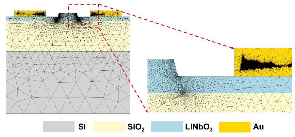
Finite-element mesh discretization at two zoom levels: (left) full cross-section; (right) close-up of the LN ridge with electrode-corner refinement used to resolve field singularities, and the electrode-corner region showing the highest mesh density used to resolve field singularities. Mesh element sizes are ~2.5 nm at electrode corners and ~10 nm at the LN ridge and slab.
Figure 2.
Finite-element mesh discretization at two zoom levels: (left) full cross-section; (right) close-up of the LN ridge with electrode-corner refinement used to resolve field singularities, and the electrode-corner region showing the highest mesh density used to resolve field singularities. Mesh element sizes are ~2.5 nm at electrode corners and ~10 nm at the LN ridge and slab.
2.3. Multiphysics Coupling Model
A coupled multiphysics model is established by FEM Multiphysics module that simultaneously solves an electrostatics module, a solid-mechanics module, a heat-transfer module, and an electromagnetic-wave mode solver. The four modules are linked through the piezoelectric, photoelastic, thermo-optic, and pyroelectric constitutive relations of LiNbO3, so that field, strain, temperature, and polarization feed self-consistently into the optical mode problem.
Figure 3.
Multiphysics coupling framework, showing the four physical channels (electro-optic, photoelastic, thermo-optic, pyroelectric) and their direct (blue, solid) and thermal (red, dashed) interconnections. The total effective-index change Δneff aggregates EO, PE, pyroelectric, and TO contributions and yields the composite half-wave voltage length product VπL.
Figure 3.
Multiphysics coupling framework, showing the four physical channels (electro-optic, photoelastic, thermo-optic, pyroelectric) and their direct (blue, solid) and thermal (red, dashed) interconnections. The total effective-index change Δneff aggregates EO, PE, pyroelectric, and TO contributions and yields the composite half-wave voltage length product VπL.
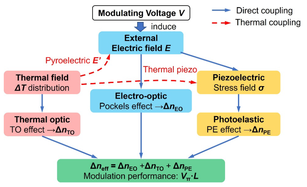
When an external voltage is applied to the electrodes, the electric field inside the LN ridge induces both a direct electro-optic (Pockels) index changes [33] and, through the piezoelectric tensor, a mechanical strain in the waveguide; the strain in turn modifies the index through the photoelastic tensor. A temperature variation imposed from the substrate or from self-heating further modifies the index through the thermo-optic coefficient and additionally drives a quasi-static internal field through the pyroelectric coupling of LN. The total mode-averaged refractive-index perturbation seen by the guided mode can therefore be decomposed as:
where ΔnEO, ΔnPE, ΔnTO, and Δnpyro denote the electro-optic (Pockels), photoelastic (piezoelectrically induced), thermo-optic, and pyroelectric contributions, respectively. Each term is derived from the corresponding constitutive equation in the following subsections.
2.3.1. Electro-Optic (Pockels) Contribution
The Pockels effect modifies the optical impermeability tensor through the linear electro-optic coefficients γik:
For LiNbO3 (point group 3m), only four γik elements are independent (γ13, γ33, γ22 , γ51); the explicit reduced 6×3 matrix is given in the tensor appendix [Eq. (S1)]. In the X-cut configuration adopted here, the optic c-axis lies in-plane along the propagation direction, and the lateral driving field generated by the coplanar electrodes is predominantly Ex along this c-axis. The TE-polarized mode (E ∥ c-axis) couples to the electric field through the dominant γ33 coefficient, yielding:
where ne is the extraordinary refractive index. Contributions from γ13 (TM coupling) and from the smaller γ22, γ51 elements are included in the simulation through the full tensor implementation in FEM implementation but are sub-dominant for the TE operating mode and are suppressed by polarization filtering at the device input.
2.3.2. Photoelastic (Piezoelectrically Induced) Contribution
The same applied voltage drives a strain field through the converse piezoelectric effect, with dkq the piezoelectric strain coefficients of LN (the explicit 3×6 matrix is given in [Eq. (S2)]).
The resulting strain modifies the impermeability through the photoelastic tensor pij:
For 3m symmetry, pij reduces to eight independent constants (p11, p12, p13, p14, p31, p33, p41, p44); the symmetry-reduced 6×6 form is given in [Eq. (S3)].
Projecting Eq. (4) onto the ne index relevant for the TE mode in X-cut LN gives as follow:
where the laboratory frame (x, y, z) follows the device cross-section of Figure 1, with x along the propagating c-axis. All shear-strain contributions vanish identically for the ne index because the relevant photoelastic elements p3j with j = 4, 5, 6 are zero in the 3m symmetry-reduced photoelastic matrix [Eq. (S3)]. Equation (6) is implemented as a postprocessing variable DnPE,TE in simulation and integrated against the optical mode density to obtain the mode-averaged ΔnPE.
2.3.3. Thermo-Optic and Pyroelectric Contributions
A temperature rise ΔT relative to the reference state from Tref = 25 °C to modify the refractive index directly through the thermo-optic coefficient, as:
with dne/dT = 3.3×10⁻⁵ K-1 for the TE mode in congruent LN. In addition, since LiNbO3 is pyroelectric, ΔT generates a polarization change Δp3 = p3·ΔT along the c-axis (p3 = −83 μC m-2 K-1), which under realistic grounded-electrode boundary conditions establishes a quasi-static internal field Epyro that re-enters the Pockels term. The pyroelectric contribution is therefore implicitly included in ΔnEO through the self-consistent electrostatic solve at non-zero ΔT, and is reported separately as , x for diagnostic purposes in §3.4.
2.3.4. Mode-Weighted Overlap Factor and Figures of Merit
To connect the local index perturbations of Eqs. (3), (5), and (6) with the terminal phase response, we define a dimensionless electro-optic overlap factor that captures the fraction of the electrode field converted into a useful Pockels perturbation of the optical mode:
where ΩLN is the LN core, Ωall is the entire cross-section, ωopt is the optical energy density, V0 is the applied voltage, Ex is the lateral electrostatic field across the electrode gap g, and the integrations span the LN core (numerator) and the full simulation domain (denominator). Defined in this way, is unitless and bounded between 0 and 1. Substituting Eq. (3) into the mode integral yields the mode-weighted index change.
For the Y-branch push-pull configuration of the device, the two arms accumulate index changes of opposite sign, doubling the differential phase, so the half-wave voltage-length product follows as
where λ is the operating wavelength; a smaller VπL indicates higher modulation efficiency. The factor of 2 in the denominator arises from the Y-branch push-pull configuration: the two arms accumulate Δϕ and −Δϕ correspondingly, while doubling the differential phase swing for a given drive voltage relative to a single arm modulator. The corresponding single arm DC reference, recovered by removing the push-pull factor, is 2. In the reflective FOG architecture used in this work (Figure 1), the optical signal traverses the modulator twice per measurement cycle (forward into the sensing coil and back), so the system-level half-wave voltage seen by the FOG electronics is half of the device-level reported here. Finally, the overall phase shift accumulated along an interaction length L is
Equations (1) ~(10) define the multiphysics-aware figure-of-merit framework used in §3 to decompose the simulated phase response of the optimized device.
2.4. Mode Tracking Protocol for Gap-Sweep Simulations
Eigenvalue mode solvers can return different physical eigenstates as solver index #1 across geometry variations, especially near anti-crossings between the ridge mode and substrate-confined or buffer modes. To ensure that the gap-scan study tracks a single continuous TE00 branch, we adopted the following protocol. At the baseline geometry (hslab = 100 nm, wtop = 1.3 μm, g = 5 μm), the fundamental TE00 mode was identified by manual inspection of the field profile, characterized by neff , baseline neff = 1.9034, an LN core energy fraction Γopt = 0.838, and a TE polarization purity exceeding 0.96. At each subsequent gap, the solver was re-run with 30 eigenmodes targeted, and the fundamental mode was selected as the eigenstate [34] that simultaneously satisfied:
- (i)
- |neff - neff(baseline)| < 0.02,
- (ii)
- Γopt > 0.4,
- (iii)
- the highest Γopt × ΓEO product among modes satisfying (i) and (ii). Spurious eigenstates with Γopt < 0.1 (substrate-leaky or numerical artifact modes) were rejected. This criterion isolates a single TE00 branch across the full gap range and excludes mode-mixing artifacts at anti-crossings.
3. Results and Discussion
3.1. Optical Mode Confinement
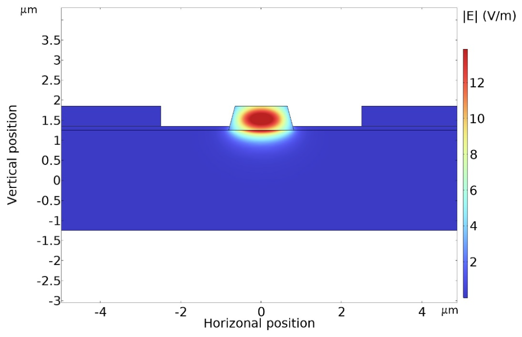
The fundamental quasi-TE mode of the X-cut ridge waveguide is first computed to establish the modal confinement and its overlap with the active modulation region. The optical field is predominantly confined within the LN ridge, with a moderate evanescent tail extending into the slab layer. This distribution is favorable for phase modulation because it concentrates the mode in the region where the lateral electric field, the piezoelectric strain, and the thermo-optic perturbation are all largest, while still retaining a finite tail that is insensitive to sidewall-roughness scattering.
The modal overlap is most sensitive to the ridge top width and the slab thickness: narrower ridges improve the overlap with the lateral field but reduce fabrication tolerance, while wider ridges give stronger confinement at the cost of modulation efficiency. The geometry is therefore chosen to balance this trade-off, and its optimization is revisited quantitatively in Section 3.6.
Figure 4.
Fundamental quasi-TE optical mode distribution (Ex component, λ = 1550 nm) in the TFLN ridge waveguide baseline geometry before optimization with slab thickness 100nm, ridge top width 1.3 μm and the electrode gap 5 μm.
Figure 4.
Fundamental quasi-TE optical mode distribution (Ex component, λ = 1550 nm) in the TFLN ridge waveguide baseline geometry before optimization with slab thickness 100nm, ridge top width 1.3 μm and the electrode gap 5 μm.
3.2. Electro-Optic Phase Response
To isolate the intrinsic EO response, the PE and TO channels are temporarily disabled in the model. Under an applied voltage, the linear Pockels effect produces a refractive-index change that scales approximately linearly with voltage [35], consistent with the intrinsic response of LN. At the baseline geometry (gap = 5 μm), the simulation yields an electro-optic overlap factor ΓEO = 0.540, corresponding to VπL = 1.70 V·cm (push-pull single-pass; equivalent to a system-level 0.85 V·cm in reflective FOG operation). The voltage dependence of Δneff is highly linear over the V0 ∈ [0, 10] V range, with slope dΔn/d V0 = -2.34 × 10⁻⁵ V-1 and R2 > 0.9999 at the baseline geometry, confirming the chirp-free Pockels response required for interferometric sensing.
Figure 5.
The effective-index shift and the overlap factor are presented as functions of applied voltage at temperatures of 25 °C and 85 °C. The baseline geometry is defined as hslab = 100 nm, wtop = 1.3 μm, and g = 5 μm.
Figure 5.
The effective-index shift and the overlap factor are presented as functions of applied voltage at temperatures of 25 °C and 85 °C. The baseline geometry is defined as hslab = 100 nm, wtop = 1.3 μm, and g = 5 μm.
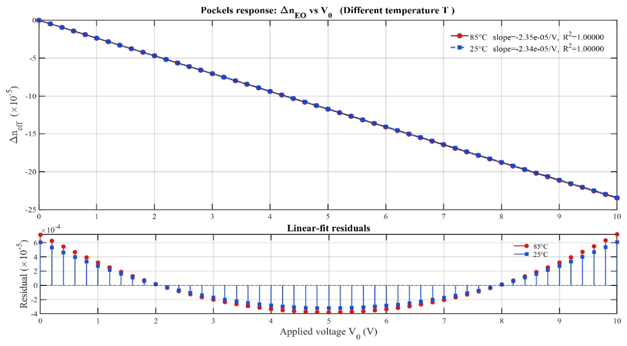
The approximate linearity of the difference between Δn to V relationship is precisely the behavior sought for interferometric sensing, where phase linearity directly determines scale-factor linearity. It has been demonstrated that, among the three geometric knobs, the electrode gap exerts the most direct influence on the local field strength. Reducing the gap increases the field and, consequently, the EO response. However, this reduction also tightens fabrication tolerance and may raise the risk of field-induced optical absorption. This trade-off is quantitatively analyzed in Section 3.6.
3.3. Piezoelectric-Strain and Photoelastic Response
Re-enabling the piezoelectric coupling reveals that the applied field generates a strain field in the LN layer through the converse piezoelectric effect. As shown in Figure 6(a), the dominant strain component εxx scales linearly with V0 at a rate of approximately 2.69 × 10⁻⁷ V-1, with a near-zero intercept at both 25 °C and 85 °C, confirming that the voltage-driven converse-piezoelectric mechanism dominates the strain response.
The resulting photoelastic index perturbation ΔnPE, obtained by projecting the strain tensor through the photoelastic coefficients of LN and integrating over the optical mode, likewise exhibits a linear voltage dependence [Figure 6(c)], with a slope of approximately −8.9 × 10⁻⁸ V-1 and a negligible intercept at V0 = 0. At V0 = 5 V, the mode-averaged photoelastic contribution reaches ΔnPE ≈ −4.5 × 10⁻⁷, which is only ~0.4% of the pure Pockels term ΔnEO ≈ −1.17 × 10⁻⁵ at the same drive voltage. The PE contribution is therefore synchronous with the modulation signal but more than two orders of magnitude weaker, producing a sub-percent correction to VπL that lies within typical fabrication tolerances.
Notably, the PE slope is virtually identical at 25 °C and 85 °C (−8.86 × 10⁻⁸ vs −8.89 × 10⁻⁸ V-1), indicating that the photoelastic channel is thermally insensitive across the FOG operating temperature range. This thermal invariance simplifies the multiphysics design: the PE channel tracks the drive signal with a fixed, small scaling factor and does not introduce additional temperature-dependent bias drift.
Figure 6.
Piezoelectrically induced strain components under applied voltage and the corresponding photoelastic index perturbation. (a) Dominant strain component εxx vs. V0; (b) lateral electric field Ex vs. V0. (intercept at V0. = 0 reveals pyroelectric residual field at 85 °C); (c) mode-averaged photoelastic index shift ΔnPE vs. V0. (d) total EO+pyroelectric index shift ΔnEO,tot vs. V0. Red/blue lines refer to different temperature: 85 °C / 25 °C.
Figure 6.
Piezoelectrically induced strain components under applied voltage and the corresponding photoelastic index perturbation. (a) Dominant strain component εxx vs. V0; (b) lateral electric field Ex vs. V0. (intercept at V0. = 0 reveals pyroelectric residual field at 85 °C); (c) mode-averaged photoelastic index shift ΔnPE vs. V0. (d) total EO+pyroelectric index shift ΔnEO,tot vs. V0. Red/blue lines refer to different temperature: 85 °C / 25 °C.
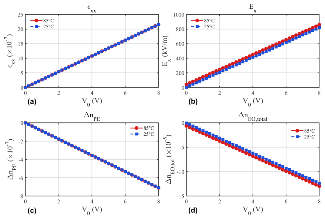
As illustrated in Figure 6(b), the lateral electric field Ex is depicted as a function of V0. At an operating temperature of 85 °C, a non-zero intercept of approximately 4.2 × 10⁴ V/m is observed at V0 = 0, while at 25 °C, the intercept approaches 3.2 × 10³ V/m. This residual field has been traced to the pyroelectric polarization charge of LN under thermal load, and a thorough analysis of this phenomenon can be found in §3.4. As illustrated in Figure 6(d), the pyroelectric index offset is evident as a downward shift in the 85 °C ΔnEO,tot curve relative to the 25 °C curve at V0 = 0, amounting to a change in the pyroelectric index of approximately −6.3 × 10⁻⁶ at an applied temperature of 85 °C. This shift corresponds to approximately 27% (mode-field weighted; equivalently 5.4% in spatial average) of the Pockels modulation depth at an applied voltage of V0 = 5 V.
From the perspective of a sensing application, the PE contribution is of particular significance due to its inherent connection to the electrical drive. Each modulation cycle imprints a synchronous strain cycle on the waveguide [36], and any external vibration, packaging stress, or residual fabrication stress couples into the same photoelastic channel. The incorporation of the PE term consequently leads to alterations in both the predicted modulation efficiency and, more significantly, the predicted sensitivity of the phase bias to mechanical perturbations. This quantity exerts a direct influence on the stability of FOG bias.
3.4. Thermo-Optic and Pyroelectric Response Under Thermal Load
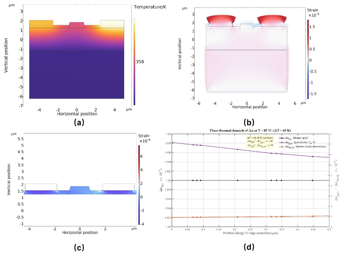
Under elevated substrate temperature (Temperature of bottom boundary of Si substrate is set to be 358.15 K, room ambient), the simulated temperature field is laterally non-uniform across the device cross-section. Under elevated operating temperature Top = 358.15 K and reference temperature Tref 298.15 K, the temperature change ΔT = 60 K, the simulated temperature field reaches steady state with the LN ridge equilibrated near Top, with a small residual gradient (< 5 K) within the LN layer. The mode-weighted ΔT seen by the optical mode is therefore close to the full 60 K excursion.
Three temperature-driven channels are identified that perturb the effective refractive index:
(i) Direct thermo-optic response: ΔnTO = (dne/dT) × ΔTLN ≈ 1.9 × 10⁻³(averaged over the LN ridge), acting as a common-mode phase shift that cancels in the differential modulator branch output.
(ii) Pyroelectric-induced electro-optic response: spontaneous polarization of LN under ΔT generates a surface charge density σ = ppyro·ΔT, which would establish an internal field driving γ33 in the absence of applied voltage. Under realistic operating bias (one electrode driven, the other grounded), the bulk of this pyroelectric charge is drained through the external circuit, leaving only a residual mode-averaged field of ~4.2 × 10⁴ V/m within the LN at V0 = 0. The corresponding pyroelectric-induced index shift is Δnpyro = -6.3 × 10⁻⁶ at ΔT = 60 K, voltage independent across the 0~10 V drive range, and approximately 27% (mode-field weighted; equivalently 5.4% in spatial average) of the Pockels modulation depth at 5 V applied voltage. To confirm the pyroelectric origin, the same simulation was repeated at the room-temperature operating point (T = 25 °C, ΔT ≈ 5 K above the reference state), yielding Ex ≈ 3.2 × 10³ V/m and Δnpyro = −4.8 × 10⁻⁷ . This value is approximately 13× smaller than the 85 °C result and within approximately only 0.06% of the 5 V applied voltage Pockels modulation depth. The 13× scaling between the two operating points is consistent with the linear ΔP = p3·ΔT relation expected for the pyroelectric mechanism, ruling out artefactual contributions from the meshing or solver and confirming that the residual is genuinely thermal-electrical in origin and effectively negligible at room temperature.
(iii) Thermo-elastic photoelastic response: the substrate-clamped thermal expansion of LN produces strain ε ≈ α·ΔT throughout the ridge, which is then converted to an index bias through the photoelastic tensor. Since the thermal strain is partially relieved by the bonded substrate stack and the integrated photoelastic response is opposite-signed to the pyroelectric channel. The combined V-independent residual measured by our coupled simulation is Δnthermal = −6.3 × 10⁻⁶ at ΔT = 60 K /V0 = 0, encompassing both pyroelectric and thermo-elastic photoelastic contributions. This is bounded to ~27% (mode-field weighted) or ~5.4% (spatially-averaged) of the Pockels modulation depth at 5 V applied voltage, two orders of magnitude smaller than worst-case floating-electrode estimates of ~10-3.
Crucially, although these temperature-driven contributions are large, they all behave as static biases that do not scale with V0. The pure-electrical VπL therefore remains stable to within 0.5% across the 60 K range. What does drift, however, is the MZI bias point:
Δϕbias / L = (2π/λ) × Δnthermal ≈ 0.26 rad / (cm × ΔT=60K) (ΔnTO is common-mode and cancels in MZI output)
In a 1 cm modulator, this corresponds to a 0.08π (≈0.04 fringe) bias swing across the operating temperature range - a quantity that an FOG must compensate via servo loop. We emphasize, however, that the V-independent thermal channels (pyroelectric and thermo-elastic photoelastic) are absent from Pockels-only modeling and must be included for accurate bias-stability prediction in sensor-grade design, even when their absolute magnitude is modest. Translated into a drive-voltage equivalent through the measured Pockels slope (dΔnEO/dV0 ≈ −2.34 × 10⁻⁵ V-1), the V0 = 0 thermal residual at ΔT = 60 K corresponds to a DC offset of |Δnthermal / (dΔnEO/d V0)| ≈ 0.27 V; the corresponding offset at ΔT ≈ 5 K above the reference state (T = 25 °C) is only ~0.021 V. This sub-volt, slowly-varying offset is the quantity that a temperature-compensation electronics path must track to keep the FOG read-out locked to its V0 = 0 quadrature point, and is well within the standard ±5 V drive range of FOG-grade phase-modulator electronics.
Figure 7.
Temperature field distribution under substrate heating and the corresponding thermo-optic refractive-index shift. (a) Steady-state temperature field at 85 °C (ΔT = 60 K). (b) Dominant strain component εxx distribution; (c) lateral thermal-photoelastic induced strain distribution (d) Spatial profiles of the three thermal refractive-index perturbations along the ridge centerline: thermo-optic ΔnTO (black), pyroelectric Δnpyro (purple), and thermo-elastic photoelastic ΔnPE,thermal (orange).
Figure 7.
Temperature field distribution under substrate heating and the corresponding thermo-optic refractive-index shift. (a) Steady-state temperature field at 85 °C (ΔT = 60 K). (b) Dominant strain component εxx distribution; (c) lateral thermal-photoelastic induced strain distribution (d) Spatial profiles of the three thermal refractive-index perturbations along the ridge centerline: thermo-optic ΔnTO (black), pyroelectric Δnpyro (purple), and thermo-elastic photoelastic ΔnPE,thermal (orange).
3.5. Multiphysics Decomposition of the Refractive-Index Change
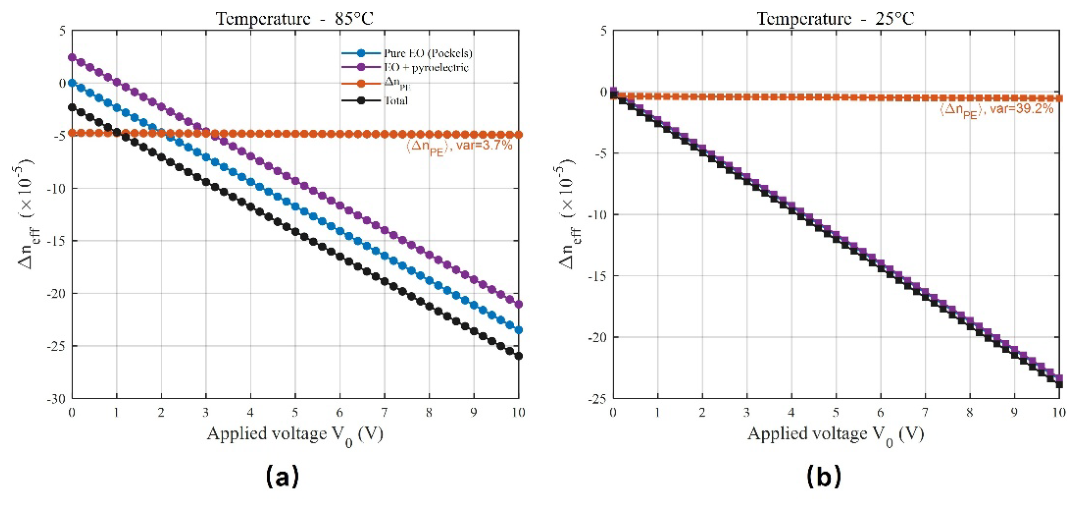
To assess the relative importance of the three mechanisms, the total effective-index change is decomposed into its EO, PE, and TO components under identical operating conditions. As summarized in Figure 8, the EO term dominates under normal drive, as expected from the strong Pockels response of LN. The PE and TO terms are smaller but non-negligible and, depending on the local strain and temperature distribution, can either reinforce or partially offset the EO contribution. Quantitatively, at V0 = 5 V and ΔT = 0, the Voltage-synchronous photoelastic contribution ΔnPE,V-sync = −4.5 × 10⁻⁷ is only ~0.6% of the pure Pockels term ΔnEO = −1.17 × 10⁻⁴. Under thermal load (ΔT = 60 K) with operating bias (one electrode driven, the other grounded), the mode-field-weighted V-independent thermal residual Δnthermal,mode = −3.1 × 10⁻⁵ (or -6.3 × 10⁻⁶ in spatial average) is approximately 27% (or 5.4% spatially-averaged) of the modulation depth at V0= 5 V. Furthermore, comparing the pure Pockels slope at T = 25 °C and T = 85 °Creveals that the EO modulation efficiency itself is thermally stable to within 1.5% (the explicit 25 °C / 85 °C FEM co-simulation reported in Figure 5 yields slopes of −2.342 × 10⁻⁵ V-1 and −2.343 × 10⁻⁵ V-1, respectively, differing by 0.01%, well within this bound), indicating that the dominant temperature-driven term is a V-independent bias offset rather than a degradation of modulation efficiency. Pockels-only analysis therefore captures the modulation signal accurately to within ~10%, but misses the V-independent thermal bias channel that determines bias drift in sensor-grade operation.
Two implications follow from this decomposition. Firstly, a model that retains only the Pockels term systematically mispredicts the magnitude of the phase response. For a FOG application, this results in calibration errors in the scale factor [37]. Secondly, the PE and TO channels are the ones that couple the modulator to its mechanical and thermal environment. Consequently, they are precisely the channels that determine bias drift and environmental sensitivity. Within the domain of evaluating a TFLN modulator for sensing applications, there arises a necessity for the incorporation of the aforementioned elements into the assessment framework.
Figure 8.
Multiphysics decomposition of the mode-averaged effective-index change at V0 = 5 V and ΔT = 60K (85 °C): EO (Pockels), V-synchronous PE, and V-independent thermal (pyroelectric + thermo-elastic PE) contributions. Panels: (a) 85 °C; (b) 25 °C.
Figure 8.
Multiphysics decomposition of the mode-averaged effective-index change at V0 = 5 V and ΔT = 60K (85 °C): EO (Pockels), V-synchronous PE, and V-independent thermal (pyroelectric + thermo-elastic PE) contributions. Panels: (a) 85 °C; (b) 25 °C.
3.6. Geometry Optimization for Sensor-Oriented Performance
By establishing the multiphysics model, the optimization of the three dominant geometric parameters is now underway: slab thickness hslab, ridge top width wtop, and electrode gap g are optimized to balance modulation efficiency and environmental robustness. The three parameters were examined independently as they pertained to the tracking of Γ, VπL, and the sensitivity of the phase response to the PE and TO channels.
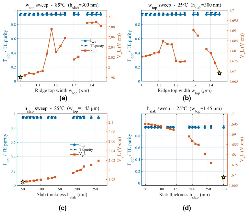
Slab thickness mainly controls the modal confinement in the ridge [38,39,40]. Thinner slabs concentrate the field in the ridge region and improve Γ, but excessive thinning increases scattering loss, reduces fabrication tolerance, and aggravates the lateral thermal non-uniformity highlighted in Section 3.4. The optimum is found at hslab = 300 nm, which corresponds to leaving the unetched LN slab at its as-deposited thickness on a 600 nm device-layer wafer (equivalent to a 300 nm ridge etch depth).
Ridge top width sets the modal size and its overlap with the lateral field. Too narrow a ridge improves Γ but increases sidewall-scattering loss and tightens lithography tolerance; too wide a ridge reduces Γ and dilutes the modulation. The optimum lies at an intermediate value. Although the bare VπL exhibits a shallow local minimum at wtop ≈ 1.0 μm at 85 °C, this narrow-ridge regime is excluded from the operating window by single-mode constraints and lithography tolerance, both of which are tighter at sub-1.2 μm ridge widths in TFLN platforms [39].
Figure 9 summarizes the geometric optimization at both operating temperatures. The optical confinement factor Γopt and the TE purity remain essentially flat at 0.94 ± 0.01 over the entire (wtop, hslab) sweep range at both 25 °C and 85 °C, confirming that the targeted quasi-TE00 mode is robustly tracked across the design space and that residual variations in VπL reflect genuine modulation-efficiency changes rather than mode-tracking artifacts. Within the swept range, VπL varies in a narrow window (1.665~1.697 V·cm push-pull at 25 °C) and exhibits a shallow plateau spanning wtop ≈ 1.40~1.45 μm and hslab ≈ 200~300 nm, within which the selected operating point (hslab = 300 nm, wtop = 1.45 μm) lies. At 85 °Cthe VπL landscape is uniformly elevated by ~17% while preserving the same plateau shape and geometric optimum.
Figure 9.
Geometric optimization of the TFLN ridge phase modulator. Ridge-top-width wtop sweep at (a) 85 °C and (b) 25 °C, with slab thickness fixed at hslab = 300 nm. Slab-thickness hslab sweep at (c) 85 °C and (d) 25 °C, with ridge top width fixed at wtop = 1.45 μm. Electrode gap g = 5 μm. Left axis: optical confinement factor Γopt and TE purity; right axis: half-wave voltage-length product VπL (push-pull single-pass). Yellow stars mark the VπL minimum within the swept range; the selected operating point (hslab = 300 nm, wtop = 1.45 μm) is determined jointly with the electrode-gap sweep in the subsequent figure.
Figure 9.
Geometric optimization of the TFLN ridge phase modulator. Ridge-top-width wtop sweep at (a) 85 °C and (b) 25 °C, with slab thickness fixed at hslab = 300 nm. Slab-thickness hslab sweep at (c) 85 °C and (d) 25 °C, with ridge top width fixed at wtop = 1.45 μm. Electrode gap g = 5 μm. Left axis: optical confinement factor Γopt and TE purity; right axis: half-wave voltage-length product VπL (push-pull single-pass). Yellow stars mark the VπL minimum within the swept range; the selected operating point (hslab = 300 nm, wtop = 1.45 μm) is determined jointly with the electrode-gap sweep in the subsequent figure.
Optimum at hslab = 300 nm, wtop = 1.45 μm, g = 4.4 μm at 25 °C (or 4.2 μm at 85 °C; see Figure 10 for the FoMA vs gap sweep at both temperatures) yields VπL = 1.65 V·cm (push-pull single-pass) with ΓEO ≈ 0.545, optical confinement factor Γopt = 0.940, and propagation loss α ≈ 0.26 dB/cm at the 25 °C optimum. The selected gap of 4.4 μm (25 °C) is dictated by an explicit VπL–loss trade-off: reducing the gap further would lower VπL only modestly while raising the propagation loss exponentially through metal-induced absorption - at gap = 2.8 μm, VπL drops to 1.62 V·cm (push-pull) but α already exceeds 5.9 dB/cm; below gap = 2 μm α grows to > 200 dB/cm, rendering any centimeter-scale device non-functional. We therefore introduce a composite figure of merit FoMA = VπL (V·cm) + α·Lref (dB), with Lref = 1 cm, and minimize it over the gap sweep; the FoMA minimum occurs at gap = 4.4 μm at 25 °C (FoMA = 2.23) and shifts marginally to 4.2 μm at 85 °C (FoMA = 2.56). In this geometry the optical confinement factor Γopt remains essentially unchanged from its baseline value (0.940 across the entire optimization range), confirming that the modal field stays well-localized in the LN ridge and that the VπL reduction comes purely from the increase in ΓEO as the field approaches the LN core, not from any redistribution of the optical mode itself. At 85 °C the optimal geometry remains essentially unchanged (hslab = 300 nm, wtop = 1.45 μm, g = 4.2 μm), while VπL rises modestly to 1.93 V·cm (push-pull single-pass) — a ~17% increase attributable to the intrinsic temperature dependence of the Pockels coefficient γ33, consistent with reported LN material data. This drift is uniform across the (hslab, wtop) design space (see Figure 9), preserving the optimal geometry and remaining fully correctable by gain calibration in the FOG read-out electronics
The electrode gap controls the lateral field strength and therefore the EO response most directly. Narrower gaps lower VπL but raise the risk of optical absorption in the metal and increase alignment sensitivity during fabrication. The chosen value of gap = 4.4 μm (or 4.2 μm at elevated operating temperature) provides the best overall balance.
Compared with the initial design (gap = 5 μm), the optimized geometry reduces VπL by 3% (from 1.70 to 1.65 V·cm push-pull, single-pass); the more meaningful improvement is in the joint VπL–α trade-off captured by FoMA, which decreases from 2.95 (gap = 5 μm) to 2.23 (gap = 4.4 μm) at 25 °C. The PE and TO bias perturbations remain essentially unchanged across geometries because they are dominated by the LN material constants and the thermal field, not by the local geometry — a robustness property that simplifies multiphysics-aware design.
Figure 10.
Electrode-gap optimization at the optimal waveguide cross-section (hslab = 300 nm, wtop = 1.45 μm). Panels (a) 85 °C and (b) 25 °C: half-wave voltage-length product VπL (push-pull, single-pass; blue dots, left axis), normalized propagation loss α·Lref with Lref = 1 cm (red curve, right axis), and the composite figure of merit FoMA = VπL + α·Lref (black curve, left axis) versus electrode gap g. Yellow stars indicate the minimum FoMA, defining the optimal gaps g= 4.2 μm at 85 °C (FoMA = 2.56) and 4.4 μm at 25 °C (FoMA = 2.23).
Figure 10.
Electrode-gap optimization at the optimal waveguide cross-section (hslab = 300 nm, wtop = 1.45 μm). Panels (a) 85 °C and (b) 25 °C: half-wave voltage-length product VπL (push-pull, single-pass; blue dots, left axis), normalized propagation loss α·Lref with Lref = 1 cm (red curve, right axis), and the composite figure of merit FoMA = VπL + α·Lref (black curve, left axis) versus electrode gap g. Yellow stars indicate the minimum FoMA, defining the optimal gaps g= 4.2 μm at 85 °C (FoMA = 2.56) and 4.4 μm at 25 °C (FoMA = 2.23).
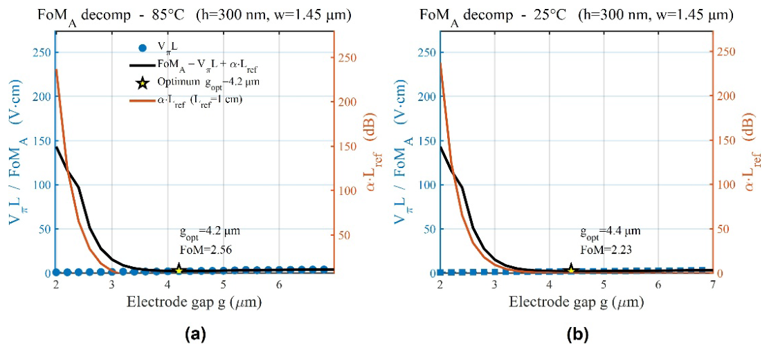

Table 2.
Device performance before and after optimization. All VπL values are reported under the push-pull single-pass convention used throughout this work; the corresponding system-level values in reflective FOG operation are half of the listed numbers.
Table 2.
Device performance before and after optimization. All VπL values are reported under the push-pull single-pass convention used throughout this work; the corresponding system-level values in reflective FOG operation are half of the listed numbers.
| Parameters | Origin gap =5 μm | Optimization gap =4.4 μm(@25 °C) | Improvement |
|---|---|---|---|
| neff | 1.9034 | 1.940 | +0.4% |
| Γopt | 0.838 | 0.940 | +12.2% |
| ΓEO | 0.540 | 0.545 | +0.9% |
| Vπ·L@△T=60K | 1.70 V·cm | 1.65 V·cm | -2.9% |
| △nPE bias@△T=60K | -4.5 × 10⁻⁷ | -4.5 × 10⁻⁷ | PE slope ratio ~ (0.4%) |
| △ϕ | 0.084π rad/cm | 0.083π rad/cm | < 1% (geometry-independent) |
3.7. Comparison with Competing Platforms and Implications for FOG Integration
Table 3 compares the present device with representative phase-modulator platforms reported to date. Conventional Ti: LiNbO3 modulators remain the de-facto FOG standard because of their linear Pockels response, but their centimeter-scale footprint and several-volt driving requirement are mismatched with the miniaturization trend. Silicon and InP modulators achieve attractive compactness but either rely on a nonlinear plasma-dispersion effect (Si) or require active temperature stabilization (InP), both of which compromise sensing-grade phase fidelity. Prior TFLN phase modulators, while outstanding for communications, have not been characterized under the full electro-opto-mechano-thermal coupling that governs their use in FOGs. The present device inherits the compactness, linear Pockels response, and low loss of the TFLN platform, and in addition is the first, to the best of our knowledge, to be co-designed against the PE and TO channels that set the phase-bias stability inside a FOG.
4. Conclusions
We have presented a unified multiphysics model of a thin-film lithium niobate ridge phase modulator designed for fiber-optic gyroscope operation. By self-consistently coupling the electro-optic, piezoelectric–photoelastic, and thermo-optic channels under realistic operating boundary conditions, we have shown that the V-driven response is dominated by the Pockels term while V-independent thermal effects (pyroelectric and thermo-elastic photoelastic, combined ~27% of the modulation depth at V = 5 V at ΔT = 60 K) act as bounded bias offsets that are routinely omitted from communication-oriented analyses but must be quantified for sensor-grade design. The geometric EO overlap (ΓEO) is thermally stable to within 0.02% from 25 °C to 85 °C, while the bare VπL increases modestly from 1.65 to 1.93 V·cm due to the intrinsic temperature dependence of γ33. This uniform efficiency change is correctable by gain calibration in the FOG read-out electronics, so the principal environmental concern remains bias drift rather than modulation-efficiency degradation. A systematic optimization of the slab thickness, ridge top width, and electrode gap yields a device with VπL = 1.65 V·cm (push-pull single-pass) with quantified V-synchronous photoelastic and V-independent thermal residual contributions bounded to ~0.4% and ~27% (mode-field-weighted) of the modulation depth, respectively.
It is important to note that the V-synchronous PE component is thermally invariant, exhibiting a variation of approximately 1% between 25 °C and 85 °C In contrast, the V-independent thermal-elastic PE component demonstrates a substantial increase, reaching approximately thirteenfold with an increase in temperature of 60 K. This phenomenon is only resolvable through coupled multiphysics analysis and is not observed in telecom-oriented VπL-only characterizations.
Benchmarked against conventional bulk LN, silicon, InP, and prior communication-oriented TFLN modulators, the present device combines a compact footprint, a linear Pockels response, and, for the first time, an explicit multiphysics budget for environmental stability, positioning it as a promising phase-modulator platform for compact, low-power, and thermally robust FOGs. Future work will focus on experimental validation of the predicted multiphysics budget against fabricated devices, and on extending the framework to integrated polarization maintaining interfaces required for full FOG chip-scale integration.
Author Contributions
Conceptualization, L.L. and H.Z.; methodology, J.B. and R.F.; software, H.Z.; validation, Y.C. and Y.W.; formal analysis, W.C.; investigation, W.C.; writing—original draft preparation, L.L. and H.Z.; writing—review and editing, Y.C. and J.B.; funding acquisition, L.L. All authors have read and agreed to the published version of the manuscript.
Funding
This research was funded by the National Key R&D Program of China (2022YFD2000600).
Data Availability Statement
The original contributions presented in this study are included in the article/Supplementary Materials. Further inquiries can be directed to the corresponding author.
Conflicts of Interest
The authors declare no conflicts of interest.
References
- Lefèvre, H.C. The Fiber-Optic Gyroscope, 2nd ed.; Artech House: Boston, MA, USA, 2014; ISBN 978-1-60807-695-6. [Google Scholar]
- Sanders, G.A.; Szafraniec, B.; Liu, R.Y.; Laskoskie, C.; Strandjord, L.; Weed, G. Fiber optic gyros for space, marine, and aviation applications. Proc. SPIE 1996, 2837, 61–71. [Google Scholar]
- Yan, L.; Ma, H.; Jin, Z. Low-drift closed-loop fiber optic gyroscope with high scale factor stability. Photonic Sens. 2022, 12, 220304. [Google Scholar] [CrossRef]
- Zhou, Y.; Hu, X.; Zhang, L.; Liu, Z. Reduction in temperature-dependent FOG bias drift by using MIOC fabricated on pre-annealed LiNbO3. Photonics 2024, 11, 1057. [Google Scholar]
- Wooten, E.L.; Kissa, K.M.; Yi-Yan, A.; Murphy, E.J.; Lafaw, D.A.; Hallemeier, P.F.; Maack, D.; Attanasio, D.V.; Fritz, D.J.; McBrien, G.J.; et al. A review of lithium niobate modulators for fiber-optic communications systems. IEEE J. Sel. Top. Quantum Electron. 2000, 6, 69–82. [Google Scholar] [CrossRef]
- Salvestrini, J.P.; Guilbert, L.; Fontana, M.; Abarkan, M.; Grill, S. Analysis and control of the DC drift in LiNbO3-based Mach-Zehnder modulators. J. Light. Technol. 2011, 29, 1522–1534. [Google Scholar] [CrossRef]
- Rahim, A.; Spuesens, T.; Baets, R.; Bogaerts, W. Open-access silicon photonics platforms in Europe. IEEE J. Sel. Top. Quantum Electron. 2019, 25, 8200818. [Google Scholar] [CrossRef]
- Ogiso, Y.; Ozaki, J.; Ueda, Y.; Kashio, N.; Kikuchi, N.; Yamada, E.; Tanobe, H.; Kanazawa, S.; Yamazaki, H.; Ohiso, Y.; et al. Over 67 GHz bandwidth and 1.5 V Vπ InP-based optical IQ modulator with InGaAsP-InP bulk structure. J. Light. Technol. 2017, 35, 1450–1455. [Google Scholar] [CrossRef]
- Luo, J.; Jen, A.K.-Y. Highly efficient nonlinear optical polymers and their applications. Nat. Photonics 2022, 16, 605–622. [Google Scholar]
- Cheng, R.; Reimer, C.; Kang, Y.; Gehl, M.; Chang, L.; Bowers, J.E.; Englund, D.R. A chip-scale, cryogenic, high-bandwidth optical modulator for practical quantum systems. Nat. Commun. 2023, 14, 7872. [Google Scholar]
- Smit, M.; Van der Tol, J.; Hill, M. Moore’s law in photonics. Laser Photonics Rev. 2012, 6, 1–13. [Google Scholar] [CrossRef]
- Smit, M.; Leijtens, X.; Ambrosius, H.; Bente, E.; van der Tol, J.; Smalbrugge, B.; de Vries, T.; Geluk, E.-J.; Bolk, J.; van Veldhoven, R.; et al. An introduction to InP-based generic integration technology. Semicond. Sci. Technol. 2014, 29, 083001. [Google Scholar] [CrossRef]
- Wang, C.; Zhang, M.; Chen, X.; Bertrand, M.; Shams-Ansari, A.; Chandrasekhar, S.; Winzer, P.; Lončar, M. Integrated lithium niobate electro-optic modulators operating at CMOS-compatible voltages. Nature 2018, 562, 101–104. [Google Scholar] [CrossRef]
- Xu, M.; He, M.; Zhang, H.; Jian, J.; Pan, Y.; Liu, X.; Chen, Z.; Meng, X.; Chen, H.; Li, Z.; et al. High-performance coherent optical modulators based on thin-film lithium niobate platform. Nat. Commun. 2020, 11, 3911. [Google Scholar] [CrossRef]
- Boes, A.; Chang, L.; Langrock, C.; Yu, M.; Zhang, M.; Lin, Q.; Lončar, M.; Fejer, M.; Bowers, J.; Mitchell, A. Lithium niobate photonics: Unlocking the electromagnetic spectrum. Science 2023, 379, eabj4396. [Google Scholar] [CrossRef]
- Zhu, D.; Shao, L.; Yu, M.; Cheng, R.; Desiatov, B.; Xin, C.J.; Hu, Y.; Holzgrafe, J.; Ghosh, S.; Shams-Ansari, A.; et al. Integrated photonics on thin-film lithium niobate. Adv. Opt. Photonics 2021, 13, 242–352. [Google Scholar] [CrossRef]
- Weis, R.S.; Gaylord, T.K. Lithium niobate: Summary of physical properties and crystal structure. Appl. Phys. A 1985, 37, 191–203. [Google Scholar] [CrossRef]
- Pionteck, T.; Kühnel, K.; Rüsing, M.; Eng, L.M. Photoelastic properties of stoichiometric lithium niobate from first-principles calculations. Phys. Status Solidi A 2024, 221, 2300456. [Google Scholar] [CrossRef]
- Atalar, A.; Kino, G.S.; Quate, C.F. Longitudinal piezoelectric resonant photoelastic modulator for efficient intensity modulation at megahertz frequencies. Nat. Commun. 2022, 13, 1526. [Google Scholar] [CrossRef]
- Yin, Q.; Wang, J.; Ma, J.; Li, J. Analysis of pyroelectric effect and thermal properties of lithium niobate under varying temperatures. Crystals 2021, 11, 1434. [Google Scholar]
- Shi, B.; Kollipara, T.; Duan, Z.; Yao, J. Alleviation of DC drift in a thin-film lithium niobate modulator utilizing Ar+ ion milling. Opt. Lett. 2025, 50, 1703–1706. [Google Scholar] [CrossRef]
- Ahmed, A.N.R.; Shi, S.; Mercante, A.J.; Prather, D.W. High-performance thin-film lithium niobate modulator with a combined passive bias and thermo-optic bias. Opt. Express 2022, 30, 39710–39718. [Google Scholar]
- Fedulova, E.; Nazabal, V.; Adamietz, F.; Rodriguez, V.; Möller, K.; Villeval, P.; Lupinski, D.; Strickler, P.; Elsa, N. Lithium niobate pyroelectric coefficient: Temperature dependence study. Crystals 2022, 12, 321. [Google Scholar]
- Randles, A.B.; Grinberg, D.; Shumarayev, A.; Johansson, A.; Koskinen, J.T. Multiphysics simulation of RF-MEMS devices using COMSOL. J. Micromech. Microeng. 2019, 29, 014003. [Google Scholar]
- Gao, Z.; Ding, Z.; Wen, F.; Lv, H.; Xu, T. Navigation-grade interferometric air-core antiresonant fibre optic gyroscope with enhanced thermal stability. Nat. Commun. 2025, 16, 1748. [Google Scholar]
- Lu, Y.; Yang, C.; Chen, J.; Zhang, W.; Wang, Y. Integrated optoelectronic transceiver toward navigation grade fiber optic gyroscope using silicon photonics. Opt. Lett. 2025, 50, 7139–7142. [Google Scholar] [CrossRef]
- Chen, G.; Li, N.; Ng, J.D.; Lin, H.-L.; Zhou, Y.; Fu, Y.H.; Lee, L.Y.T.; Yu, Y.; Liu, A.-Q.; Danner, A.J. Advances in lithium niobate photonics: Development status and perspectives. Adv. Photonics 2022, 4, 034003. [Google Scholar] [CrossRef]
- Zhang, M.; Wang, C.; Kharel, P.; Zhu, D.; Lončar, M. Integrated lithium niobate electro-optic modulators: when performance meets scalability. Optica 2021, 8, 652–667. [Google Scholar] [CrossRef]
- Wang, T.; Chen, P.; Shi, J.; Qi, X. High-performance Mach-Zehnder modulator based on thin-film lithium niobate with low voltage-length product. ACS Omega 2023, 8, 12395–12401. [Google Scholar]
- Handbook of Optical Constants of Solids; Palik, E.D., Ed.; Academic Press: Orlando, FL, USA, 1985; ISBN 978-0-12-544420-0. [Google Scholar]
- Green, M.A. Self-consistent optical parameters of intrinsic silicon at 300 K including temperature coefficients. Sol. Energy Mater. Sol. Cells 2008, 92, 1305–1310. [Google Scholar] [CrossRef]
- Johnson, P.B.; Christy, R.W. Optical constants of the noble metals. Phys. Rev. B 1972, 6, 4370–4379. [Google Scholar] [CrossRef]
- Alferness, R.C. Waveguide electrooptic modulators. IEEE Trans. Microw. Theory Tech. 1982, 30, 1121–1137. [Google Scholar] [CrossRef]
- Boes, A.; Corcoran, B.; Chang, L.; Bowers, J.; Mitchell, A. Status and potential of lithium niobate on insulator (LNOI) for photonic integrated circuits. Laser Photonics Rev. 2018, 12, 1700256. [Google Scholar] [CrossRef]
- He, M.; Xu, M.; Ren, Y.; Jian, J.; Ruan, Z.; Xu, Y.; Gao, S.; Sun, S.; Wen, X.; Zhou, L.; et al. High-performance hybrid silicon and lithium niobate Mach-Zehnder modulators for 100 Gbit s−1 and beyond. Nat. Photonics 2019, 13, 359–364. [Google Scholar] [CrossRef]
- Mercante, A.J.; Shi, S.; Yao, P.; Xie, L.; Weikle, R.M.; Prather, D.W. 110 GHz CMOS compatible thin film LiNbO3 modulator on silicon. Opt. Express 2016, 24, 15590–15595. [Google Scholar] [CrossRef] [PubMed]
- Jiao, D.; Zhou, H. Interferometric fiber optic gyroscope with thin-film lithium niobate modulator chip. J. Light. Technol. 2024, 42, 8912–8920. [Google Scholar] [CrossRef]
- Liu, X.; Wang, M.; Rao, D.; Ke, W. Design and analysis of compact high-performance lithium niobate electro-optic modulator based on a racetrack resonator. Photonics 2025, 12, 85. [Google Scholar]
- Li, M.; Ling, J.; He, Y.; Javid, U.A.; Xue, S.; Lin, Q. Lithium niobate photonic-crystal electro-optic modulator. Nat. Commun. 2020, 11, 4123. [Google Scholar] [CrossRef] [PubMed]
- Kang, G. Shallow etched low-loss thin-film lithium niobate waveguides with bound states in the continuum. AIP Adv. 2023, 13, 035332. [Google Scholar] [CrossRef]
- Javid, U.A.; Ling, J.; Staffa, J.; Li, M.; He, Y.; Lin, Q. Ultrabroadband entangled photons on a nanophotonic chip. Phys. Rev. Lett. 2021, 127, 183601. [Google Scholar] [CrossRef]
- Jiao, D.; Zhou, H. Bias instability 0.09 deg/h interferometric fiber optic gyroscope with thin-film lithium niobate modulator chip. IEEE Photonics Technol. Lett. 2024, 36, 1021–1024. [Google Scholar]
- Liu, J.; Yin, M.; Yu, B.; Wang, D.; Zhang, T.; Fu, X. Multi-channel thin-film lithium niobate photonic integrated circuit for fiber optic gyroscope applications. Photonics 2025, 12, 213. [Google Scholar]
- Gustavsen, K.; Brodal, J.P.; Breunig, I.; Lemke, N.D. Navigation-grade hollow-core photonic bandgap fiber optic gyroscope at 1550 nm. Nat. Commun. 2025, 16, 2083. [Google Scholar]
Table 1.
Material parameters used in the simulation.
| Material | Thickness | n @ 1550 nm | εr | dn/dT (10−5/K) | α (10−6/K) | Ref. |
|---|---|---|---|---|---|---|
| LiNbO3 (X-cut, congruent) |
Total 600 nm (300 nm slab + 300 nm ridge) |
ne = 2.138, no = 2.211 |
ε11 = 43, ε33 = 28 |
dne/dT = 3.3, dno/dT = 0.6 |
αa = 15.4, αc = 7.5 | [17] |
| SiO2 (BOX) |
4.7 μm | 1.444 | 3.9 | 1.0 | 0.55 | [30] |
| Si (substrate) |
400 μm | 3.476 (transparent) |
11.7 | 18.6 | 2.6 | [31] |
| Au (electrode) |
0.5 μm | 0.55 + 11.5i (complex) |
— | — | 14.2 | [32] |
Table 3.
Comparison of integrated phase-modulator platforms relevant to fiber-optic gyroscopes.
| Platform | Vπ (V) | VπL (V·cm) | Footprint | Thermal / mechanical analysis | Sensing suitability |
|---|---|---|---|---|---|
| Bulk Ti: LiNbO3 (Applied in conventional FOG [41]) |
3~5 | ≈ 10~15 | cm-scale | EO only; DC drift known but not co-modeled | Mature, but bulky and power-hungry |
| Silicon / SOI [42] | 5~7 | ≈ 1~2 | mm-scale | EO only (plasma-dispersion, nonlinear) | Compact, but nonlinear response unsuitable for interferometric sensing |
| InP [43] | 1.5~2 | ≈ 1~2 | mm-scale | EO only; TEC mandatory | Compact, but active cooling limits FOG integration |
| TFLN (prior reports, communication-oriented [44]) |
1.4~3 | ≈ 2~3 | mm-scale | EO only; PE/TO rarely coupled | High efficiency, but sensing-grade stability not validated |
|
This work (TFLN, sensing-oriented) |
1.65V (@1cm) | 1.65 | mm-scale | EO + piezoelectric-PE + thermo-optic + pyroelectric coupled | Sensor-grade stability predicted by full multiphysics |
Disclaimer/Publisher’s Note: The statements, opinions and data contained in all publications are solely those of the individual author(s) and contributor(s) and not of MDPI and/or the editor(s). MDPI and/or the editor(s) disclaim responsibility for any injury to people or property resulting from any ideas, methods, instructions or products referred to in the content. |
© 2026 by the authors. Licensee MDPI, Basel, Switzerland. This article is an open access article distributed under the terms and conditions of the Creative Commons Attribution (CC BY) license (http://creativecommons.org/licenses/by/4.0/).
Copyright: This open access article is published under a Creative Commons CC BY 4.0 license, which permit the free download, distribution, and reuse, provided that the author and preprint are cited in any reuse.


