Submitted:
19 February 2026
Posted:
26 February 2026
You are already at the latest version
Abstract
CdSe-coated electrodes, formed by electrodeposition of CdSe barrier layers on metallic Ti or porous TiO2 substrates were characterized by electrochemical impedance spectroscopy in a (photo)cell with aqueous redox electrolytes based on the sulfide/polysulfide and ferro/ferricyanide couples. Common to the metallic and oxide substrate electrodes, the shape and features of Mott–Schottky plots were found to be influenced by the electrode material properties, the electrolyte contact, and measurement conditions (illumination, frequency, potential-scan speed). The information obtained from capacitance measurements are evaluated on the basis of the ideal Schottky-diode model and photocurrent voltammetry data. The rationale behind the observed non-idealities is inquired, and peculiarities of the measuring procedure connected to the non-stationary character of the interface are discussed.
Keywords:
Mott–Schottky
; electrochemical impedance
; cadmium selenide
; titanium oxide
; electrodeposition
; photocurrent voltammetry
1. Introduction
The energetics at a semiconductor/electrolyte (SC/EL) interface, i.e., Fermi level, band edge positions, space charge layer width, and related parameters, can be sought through differential capacitance (C) measurements by means of electrochemical impedance (EI) spectroscopy. For an ideal Schottky barrier interface, the Mott-Schottky relation predicts a linear dependence of the inverse square of the semiconductor depletion layer capacitance on the applied potential, with a slope that is determined by the dopant concentration [Eq. (1)].
In Eq. (1), proper for n-type semiconductor electrodes, CSC is the SC space charge capacitance, εr the relative permittivity of the SC bulk, U the electrode potential, UFB the flat band potential of the SC, ND the ionized donor concentration, and kB, T, e have their usual meaning. The well-known assumptions for an ideal Schottky barrier interface on which the derivation of Eq. (1) is based are briefly the following [1]: (i) the capacitance of the Helmholtz layer and of other possible surface layers is negligibly large; (ii) the bulk semiconductor, the contacts and the electrolyte have zero resistance; (iii) the (liquid) junction barrier has perfectly blocking properties; (iv) no surface states are present on the electrode; (v) the permittivity ε of the semiconductor is frequency-independent; (vi) only one type of completely ionized donors is present, and their spatial distribution is homogeneous; (vii) the interface is perfectly planar and the space charge region does not extend into the substrate.
Mott–Schottky analysis is widely used for rapid predictions of energetic parameters, not only for structurally precise electrodes, but also in ambiguous situations involving ill-defined materials. When attempting to characterize SC electrochemical interfaces, complications arise that are associated to the failure to satisfy one or, often, several of the assumptions that accompany the simple Schottky model. For instance, it is assumed that any potential change at the SC/EL junction appears on the SC side only, implying that the band edges of the SC are pinned at the interface. However, when charging of surface states takes over or/and the potential-drop in the Helmholtz layer is important, the Fermi level may be pinned at the interface rendering the band edges mobile. In general, the imperfect SC/EL interface lies at an intermediate state between band-edge and Fermi-level pinning, which means that the applied potential, apart from producing band bending in the SC, is partly expended to surface state charging [2,3]. The ability of surface states to store electrons creates a shunt capacitance CSS (= dQSS/dU; where QSS the charge density for surface states) in parallel with the space charge component CSC. Furthermore, the SC/EL interface is more or less a chemically unstable system, so that time-dependent effects related to corrosion processes show up during the measuring procedure. The properties of the electrolyte contact are very important in this connection.
The present work intends to an examination of polycrystalline semiconductor electrodes in (photo)electrochemical cells (PEC) employing common electrolytes by means of Mott-Schottky analysis, in order to address the deviations usually observed from the ideal diode behavior and to identify their sources. The investigation is exemplified by use of electrodes prepared by electrodeposition of CdSe barrier layers on metallic titanium or on porous titania substrates. In general, the electrodeposition and properties of CdSe on common metallic substrates (as well as on transparent conductive oxides) have been widely investigated, whereas deposition on TiO2 is more specific and comes under the scope of n-TiO2 sensitization by inorganic semiconductors [3]. In effect, CdSe has been found to extend the light-harvesting spectrum range of TiO2 [4]; however, no attempt was made here to identify TiO2 sensitization effects.
Our present concern was to examine the effect of the different microstructure and conductivity type of Ti and TiO2 substrates on the photoelectrochemical behavior of the electrodes especially with respect to impedance measurements. Specific (differential) capacitance data (C; F cm−2) were collected from impedance measurements in PEC, and plotted as inverse square capacitance (C−2) vs. applied potential. The capacitance was calculated using standard equivalent circuit for Mott–Schottky measurements. No attempt was made to obtain advanced quantitative simulations of the complex impedance response (Nyquist plots) based on multi-component equivalent circuits [5]. Ongoing research results using constant phase element simulations will be presented in a separate publication.
2. Materials and Methods
The electrochemical setup consisted in a single compartment, thermostat-controlled three-electrode cell driven by a Voltalab 40 PGZ 301 unit or a Wenking PGS 81R (Bank Electronic) potentiostat. Commercial-grade titanium metal (99.6%, ASTM grade 2) cylinders with exposed area of ca. 1.13 cm2 were used as working electrodes, a Pt grid as counter and Ag/AgCl (3 M KCl) reference (+0.207 V vs. SHE at 25 °C). Electrodeposition of CdSe was performed on rotating disc Ti electrode from an aqueous acidic (pH = 1.9) solution of 0.2 M CdSO4, 10−3 M SeO2 under potentiostatic conditions at a bath-temperature of 85 °C [6]. The Ti working electrodes were used either pretreated so as to have a clean, oxide-free surface – the treatment consisting in abrasion; polishing by alumina 0.3 μm powder; cleaning by common solvents in ultrasonic bath; etching in 10% HF solution for 10 s and thoroughly wash in water – or as-anodized in a two electrode cell (stainless steel counter) containing a 0.5% wt. HF, 1 M H3PO4 aqueous solution, to form an ordered TiO2 nanotube matrix of monodispersed 100 nm in-diameter nanotubes [4]. Water (18.3 MΩ cm), purified by an ultrapure water system (Easy Pure Barnstead RF) and as received analytical grade reagents were used for the preparation of solutions. Deposits were subjected to heat treatment in a tube furnace (Ionic System GmbH; Kiel Cell 2.0) in nitrogen atmosphere at 300 or 500 °C (heating rate: 10 °C min−1, 1 h at final temperature and natural cooling). Linear sweep voltammetry and photovoltammetry were performed at stagnant baths, in a thermostat-controlled cell at 23 °C, using a three-electrode setup (commonly Pt counter and Ag/AgCl reference or Pt pseudo-reference).
Potential-step electrochemical impedance (EI) measurements were carried out in a three-electrode photoelectrochemical cell (PEC) (Pt counter, Ag/AgCl reference or Pt pseudo-reference) driven by the Voltalab 40 PGZ 301 platform. A sulfide/polysulfide (SPS) solution (S−/Sn−2) made of 1 M Na2S, 1 M S, 1 M NaOH, and a ferro/ferricyanide (FFC) solution ([Fe(CN)6] −3/−4) made of 0.1 M K4[Fe(CN)6], 0.1 M K3[Fe(CN)6], 1 M Na2SO4 were used as redox electrolytes in the PEC. The respective background solutions, namely 1 M NaOH for SPS and 1 M Na2SO4 for FFC were also used for control experiments. For illumination of the cell, a 150 W discharge metal-halides source (color temperature 4200 K) of controllable light intensity was used; typically using an irradiance of 100 mW cm−2 (unit solar) at the surface of the active electrode. Impedance measurements were performed by sweeping the applied potential stepwise in the range from 0.0 to −0.8 V (vs. Ag/AgCl) in either 10 or 50 mV steps, using a step duration of 20 s; the superimposed ac-signal had a 10 mV sine wave amplitude and was adjusted at different constant frequencies in the range from 10 kHz to 10 mHz.
3. Results and Discussion
Stoichiometric and compact CdSe films of a zinc blende structure (JCPDS #19–0191), with a thickness of 2–3 μm, a strong (111) crystallographic texture and low roughness were obtained on Ti substrate by typical electrodeposition from an acidic selenite bath [6]. Similar CdSe barrier films of 1–2 μm thickness with weaker texture and nodular morphology were deposited on the porous titania substrates [4]. Depending on the plating specifications and post-treatment, the characteristic (Debye–Scherrer) size of the crystallite structure in the films varied from 40 to 130 nm. The CdSe/Ti and CdSe/(TiO2)Ti specimens were used as electrodes in PEC, either as-prepared without any post treatment, or after thermal annealing at various temperatures. Annealing resulted in more uniform, larger grain layers, refined from any traces of elemental Se. At calcinating temperatures above 400 °C, a wurtzite CdSe structure (JCPDS #08–0459) was established from the kinetically controlled, as-deposited zinc blende phase of CdSe.
3.1. Interface energetic
In order to extract information from EI measurements and evaluate their significance, some prior knowledge of interface energetics is needed. Characteristic energies of the electrodes, i.e., the band edge positions of CdSe films as-prepared by electrodeposition (polycrystalline; pc-films), were estimated through the flat-band potential (UFB) values as-determined from the onset potential (Uonset) in photocurrent voltammetry measurements in common electrolytes (e.g., Figure 1). The open circuit potential UOC in the dark was taken as the zero point for each measurement cell and considered equal to the redox potential for the employed electrolyte (UR/O). The UFB position was taken 0.10 V more negative than the Uonset value, on account of the electron back-diffusion current [7]. The conduction band edge (UCB) of the SC was taken as lying at −0.12 V relative to UFB [8], and the valence band edge (UVB) was located through the known value of the energetic band gap of CdSe (1.70 eV). The assessed values of UFB, UCB, and UVB are given in Table 1, along with selected data from the literature regarding n-CdSe single crystal (sc) electrodes in the respective electrolytes.
The overall resulting interface energetics is depicted in the scheme of Figure 2. It is seen that our estimated band edges for the polycrystalline electrodes are systematically shifted to slightly more positive potentials compared to those reported for single crystal electrodes; otherwise the agreement is rather good. From these data it appears that use of the depletion layer model (Mott–Schottky) is justified at the first place, since the UR/O values lie in the band gap range of the semiconductor electrode.
3.2. Different Electrolytes
Mott–Schottky plots in the dark and under illumination for CdSe/(TiO2)Ti electrodes and different liquid contacts are shown in Figure 3. The graphs were very similar for the CdSe/Ti electrodes. In these diagrams, the potential is scanned to the negative direction starting from the open circuit potential UOC in the dark taken as the zero point (actually UOC = UR/O vs Ag/AgCl). Since the SC electrode is n-type, the scan direction corresponds to a Fermi level displacement from the dark equilibrium position, towards the flat band potential UFB of the semiconductor.
It is seen in Figure 3 that the capacitance C increases in the order: FFC < Na2SO4 < NaOH < SPS, both for the dark and illuminated cells. In principle, the smaller C (higher C−2) measured in the FFC system compared to the SPS should be expected, on account of the more positive redox potential of this electrolyte (Table 1), causing larger band bending in the SC and thereby wider space charge region. Assuming that the recorded capacitance equals CSC, the U-intercepts of the plots in Figure 3 should correspond to the flat band potentials UFB vs. UOC in the dark, i.e., to the maximum band bending (UFB −UR/O) for each CdSe//electrolyte junction as given in the scheme of Figure 2. Drawing of intercept lines at the proper capacitance scale shows that the UFB vs. UOC values for the redox solutions, found at ca. −0.75 V (cf. Figure 4a for CdSe/TiO2 in SPS solution) and −1.00 V for FFC, approach those predicted in Figure 2. However, the U-intercepts for the FFC and Na2SO4 solutions are found at quite more negative values than expected from Figure 2; i.e., at −1.60 rather than −1.00 V for FFC and −0.80 rather than −0.65 V for Na2SO4. It seems that abnormally high C−2 values are involved in this case, which could be due to surface modification of the electrode during the measurement process.
Indeed, the CdSe surface in contact to FFC has been known [14] to undergo abundant formation of stable corrosion products, such as ferro-ferricyanide compounds and amorphous Se from the hole-mediated decomposition of CdSe, which add a substantial dielectric capacitance component in series to the SC space charge. It must be emphasized, however, that the absence of similar effects for SPS is only due to the fact that corrosion products build up on the electrode surface much more slowly than in the FFC case, while also any produced Se dissolves easily in the polysulfide electrolyte (Section 3.5). To be sure, the photovoltammetric (onset potential) measurements were considered more reliable, because their time scale is much smaller compared to the EI experiment, so the results in Table 1 correspond to the initially measured values, before time-dependent phenomena step in (also [2]).
Illumination of the electrodes during measurement results in an overall increase in C (decrease in C−2) at a given applied potential (Figure 3b). Considering that band-edge unpinning is very probable under conditions of intense anodic (photo)corrosion, this change of junction capacitance can be attributed to the displacement of band edges to the positive direction and consequent decrease of the band bending and space charge layer width, due to trapping of photoinduced holes at surface states. At any rate, the presence of a redox couple in the electrolyte should conduce to the stability of the system as enhancing the hole-scavenging ability for the n-type SC. “Stability” tests involving successive voltage-stepping scans were used to check each CdSe//electrolyte system. In particular, three EI recording cycles were performed involving a first scan in the dark (“dark 1”) followed by a second scan under illumination and a third again in the dark (“dark 2”). The relative increment ΔC/C between “dark 1” and “dark 2” was estimated at several selected potentials and taken as a measure of the photocorrosion effect. From “dark 1” to “dark 2”, the resulting plots always shifted to lower C−2 values, indicating that all systems are prone to photocorrosion. The SPS system was always more stable as giving a ΔC/C ratio around 1 compared to 1.5 for the FFC and the background electrolytes.
3.3. Effect of Annealing on the C−2 vs. U Plots
From the preceding remarks, it is clear that the foremost prerequisite to obtain reliable EI data is the selection of a redox electrolyte appropriate for the specific electrode type (i.e., CdSe in the present case). The C−2 vs. U plots for the SPS cell, which is the most photocorrosion-resistant system of those presently investigated, are depicted in their appropriate capacitance scale in Figure 4, for CdSe/Ti and CdSe/TiO2 electrodes, as-prepared (Figure 4a) and annealed at 500 °C (Figure 4b). Similar graphs are given in the diagrams of Figure 5 with ordinate scale normalized to unity, for as-prepared and annealed (at 300 and 500 °C) electrodes. The shapes of the plots in these diagrams are not unusual in the literature, and encompass curved rather than straight lines for the non-treated electrodes, as well as annealing-induced features on the slope and the U-axis intercept. Recall that the annealing treatment affects only the CdSe layer, while at temperatures above 400 °C, a wurtzite CdSe structure is obtained. Thermal oxidation of the Ti substrate to rutile TiO2 during treatment of CdSe/Ti must be ruled out in view of the oxygen-free annealing atmosphere.
Specifying a single slope for the curved lines in Figure 4a to estimate the active donor concentration ND in the non-treated electrodes from Eq. 1, is rather tricky. On the basis of the ideal model, and disregarding any changes of the electrode during the measurement, the shape of the plots may imply that the active donor concentration ND is not uniform across the CdSe layer and decreases with the distance from the SC/EL interface towards the SC bulk; the lower ND values correspond to the higher slope (∝ 1/ND) obtained at the more positive potentials, whereat the depletion region extends deeper in the SC electrode. After annealing the electrodes, the Mott–Schottky lines become steeper and present an upright segment at potentials positive to about −0.25 V (Figure 4b). In addition, annealed electrodes present an appreciable shift of the projected U-intercept to less negative values compared to the non-treated electrode (Figure 5), the magnitude depending on the annealing temperature.
The steep change of Mott–Schottky slope as recorded in aqueous electrolyte for electroplated polycrystalline CdSe electrodes has been addressed in the literature (e.g., [15]); however, no explanation is known to us. Within the depletion-layer approximation – cf. assumption (vi) of the ideal model – the observed segmented line shape could be interpreted by assuming either (1) the existence of two donor types, D1 and D2, in the same semiconductor phase, associated to two discrete energy levels within the bandgap, a shallow and a deep; or (2) response of both the n-type CdSe layer and TiO2 substrate, in sequence. In case (1), as the potential increases and the Fermi level moves down the energy gap, a Mott-Schottky slope of would be obtained upon reaching the shallow level, and a slope of upon reaching the deep level; this sequence would cause however a decrease in the slope, contrary to the observed. In case (2), the slope would change from to, and since the TiO2 substrate has a much lower donor concentration than CdSe, this would be in accord with the observed direction in slope change. However, comparison between the CdSe/(TiO2)Ti and CdSe/Ti electrodes (Figure 4 and Figure 5) suggests that the response regards solely the CdSe layer, since a similar slope change is observed regardless of the substrate.
Since, in general, the non-linearity of Mott–Schottky plots is largely connected to a disordered solid state structure, it can be assumed that in non-treated electrodes, the donor concentration drops gradually from the electrolyte interface towards the SC bulk due to the more defective (donor-rich) character of the upper CdSe layers, whereas in the annealed samples the ND is high at the surface contacting the electrolyte and abruptly drops in the bulk. In other words, the thermal treatment, by restoring a uniform crystallized layer, eliminates lattice imperfections with a donor character, thus steeping the Mott–Schottky plot. Calculations based on the ideal model as a rough approximation (Appendix A) may corroborate this claim, as indicating that the high donor concentration region has practically zero thickness; hence it should correspond to the inter-phase region of the CdSe//SPS contact.
The elimination of bulk donor states would be expected to move the Fermi level towards the intrinsic position in the middle of the bandgap, which explains the positive shift of the projected flat band potential (Figure 5). This model suggests that the high-slope line is representative of the bulk SC properties and allows quantitative predictions to be made from the slope and intercept of this line. On the other hand, the low-slope regions are complicated by the occurrence of surface states, which introduce energetic states close to the conduction band of the SC, presumably with density that follows an exponential decay from the band edge to lower energies within the bandgap (this “band tailing” in the polycrystalline electrode has been evidenced clearly by photocurrent spectroscopy). At the more negative potentials, charging of the surface states will make CSS the main component of the overall capacitance, and as the potential is scanned more positive and the Fermi level moves deeper in the bandgap, the exponential decrease of surface state density will be followed by an exponential increase of C−2 with potential. At some point, though, CSC dominates and a linear Mott–Schottky behavior is established [1], pretty much as the curve shape indicates. The reconstructive effect of annealing partly restores, thus, a linear behavior of the electrode at the more positive potentials, where the measured capacitance corresponds to CSC.
Further insight can be gained here with the assistance of photocurrent voltammetry (PV) data. For non-treated CdSe/Ti samples, the U-axis intercept of Figure 4a indicates a UFB lower than −0.60 V, close to the PV result (Figure 1), which gives a Uonset at about the same potential (UFB ≈ Uonset − 0.1 V). But, the PV curve for the annealed at 500 °C electrode (Figure 6) presents an appreciable photocurrent inversion from anodic to cathodic at more positive potentials, which is not observed with the non-treated electrode. In principle, the photocurrent switch signifies a transition from depletion to accumulation zone as the potential crosses the Fermi level. It occurs at approximately −0.50 (Figure 6), i.e., more negative than the claimed intercept of the upright line in Figure 4b, making the UFB estimation based on the higher slope of Figure 4b more ambiguous than considered. But, even if the quantitative agreement is not good, this result corroborates a shift of the Fermi level deeper (more positive) into the CdSe bandgap in the annealed samples. The photocurrent inversion is no longer observed already after two PV cycles so it can be considered to be implicit in the pristine CdSe phase before degradation starts in the PEC. Actually, evolving photocorrosion modifies the electrode interface, building up a dielectric Se layer (Section 3.5), which, although not restricting the anodic photocurrent as being a good hole-conductor, inhibits the cathodic photocurrent by imposing an energetic barrier to the CdSe conduction band electrons (ECB of Se lies approximately 1.0 to 1.2 eV above the ECB of CdSe [10,16]).
An alternative way to account for the uncertainty in the position of the Fermi level in terms of the photocurrent switching and the segmented appearance of the Mott–Schottky plot is to invoke the so-called Photoelectrochemical Photocurrent Switching (PEPS) effect, which describes the observed behavior as depending on the relative positions of the Fermi level and the surface state energy, rather than the position of the Fermi level itself with respect to the band edges. Hints on this effect and its significance are illustrated in the Appendix B.
3.4. Frequency Dependence and Electron Density Calculation
Impedance measurements performed with the CdSe//SPS system show strong variation of the Mott–Schottky slope with frequency, implying that the assumption (v) of the ideal model is not valid due to dielectric relaxation; that is, frequency dependence of the dielectric constant ε. When the determination of ND is not possible from a single experiment at one frequency, a slope averaging procedure can be attempted as suggested by Gomes and Cardon [1], by plotting C−2 vs. U at different EI frequencies and specifying limiting slope values: the maximum slope is given by 2/[eεoε(0)ND] and the minimum slope by 2ε(0)/[eε0εi2ND], where ε(0) and εi are the relative permittivities for zero and limiting high frequency, respectively. Since the dielectric constant drops asymptotically from ε(0) to εi, within the applied range of frequencies, the higher frequencies correspond to higher Mott-Schottky slopes [1,17]. The donor density is calculated from the geometrical average of the two limiting terms (square root of their product), which is 2/[eε0εiND].
The EI experiments were performed with successive voltage scans of varying constant frequencies in the direction from high to low frequency. In order to examine also the time dependence of the process, two series of measurements were carried out, one with 10 mV-step scans (Figure 7) and the other with 50 mV-step scans (Figure 8). The step-duration was maintained at 20 s, therefore the 50 mV sequence, allowing a faster scanning of the fixed potential range, involved a smaller number of recording points (Appendix C). At any rate, according to the Gomes–Cardon procedure, and using a high frequency relative permittivity value of εi for CdSe equal to 6.20, the donor density in the semiconductor was estimated from the 10 mV-stepping experiments as 5.39 × 1018 cm−3, and from the 50 mV-stepping experiments, as 4.36 × 1018 cm−3. These values are reasonably close to each other and indicate an approximate electron density of 5 × 1018 cm−3.
The first three cycles of the fast-scan experiments were excluded from the electron-density calculation procedure, due to the presence of a moving summit, i.e., a local capacitance drop, which appears clearly at −0.60 V during the 10 kHz cycle (Figure 8a), and moves towards −0.40 V during the subsequent two cycles (the scaling is not clear in the diagram) before disappearing (Figure 8b). This peak was absent in the “slow” experiments with the SPS system, i.e., when the voltage scans were carried out in 10 mV steps (Figure 7), and needs a special consideration.
3.5. Surface Corrosion Effects: Formation of Dielectric Layer on the Electrode
The former observation signifies an ongoing chemical modification of the CdSe electrode during measurement that becomes visible on the Mott–Schottky plots, insofar as the SPS solution is concerned, only when increasing the scan rate of the potential (by an effect analogous to redox peak amplification with higher scan rate in cyclic voltammetry). In the less “stabilizing” environment of other electrolytes, this feature is prominent even with the “slow” 10 mV-stepping scans. Thus, the slight bending observed at voltages around −0.55 V in Figure 3a for the Na2SO4 solution (TiO2 substrate), which becomes more intense with illumination (Figure 3b), may be considered to have a common origin with the peak in Figure 8a. The peak is further enhanced for annealed electrodes processed in Na2SO4 solution (Figure 9a at ca. −0.55 V) and even more intense when a Ti substrate is used instead of TiO2 (Figure 9b); in this case a broad hump can also be seen on the curve regarding the NaOH solution (at ca. −0.50 V). Overall, for fixed potential-scan rate, the peak location remains at about the same potential, independent of substrate, electrolyte, or application of thermal annealing. On the other hand, the peak height is affected by all of the previous factors inasmuch as they change the electrode conductivity and surface-hole concentration. Thus, the use of metallic Ti substrate increases the electrode conductivity and also the peak height, while a similar effect is observed when the hole-scavenging ability of the solution is low, and also upon illumination; that is, factors that increase the hole concentration at the SC surface.
The local capacitance drop observed in Figure 3, Figure 8 and Figure 9 between −0.60 and −0.40 V can be attributed to the formation of a surface dielectric layer. In their C−2 vs. U plots, recorded with potentiodynamic EI spectroscopy on anodic TiO2 layers in contact with acidic electrolyte, Bondarenko et al. [18] observed a slight bowing, similar to the one appearing at about −0.60 V in Figure 3a and b for TiO2/CdSe//Na2SO4, which they attributed to the presence of a thin layer of different composition generated on the electrode surface by H+ intercalation in the TiO2 lattice. In our case, the dielectric layer is probably amorphous selenium produced by (photo)corrosion during the measurement process; CdSe is known to undergo a hole-mediated decomposition, which is catalyzed by light [10,13,19]:
CdSe(s) + 2h+ → Cd2+(aq) + Se(s)
The dynamic features of the EI measurement process with our SC electrodes, involving a decrease in peak height and displacement of its location to more positive potentials during successive voltage scans (Figure 8a), may be illustrated by considering transitions from high to low capacitance lines as the corrosion product progressively passivates the electrode and its growth rate decreases. The elements of this analysis have been previously addressed; in their general approach, Fabregat-Santiago et al. [20] suggested that complete coverage of a SC electrode by a thin dielectric surface layer results in a parallel shift of the Mott-Schottky plot to higher C−2 values, due to capacitance drop, whereas an incomplete coverage of the electrode manifests itself as a slope increase, i.e., again a capacitance drop.
The evolution of the Mott–Schottky line is modeled in Figure 10; the 1/C2 plot follows initially the Mott–Schottky line of the bare CdSe electrode (dashed line 1) and gradually, as the scan proceeds towards negative potentials, goes over the dashed line 2 of a completely (Figure 10a) or partly covered electrode (Figure 10b). The transition is accompanied by a curve bending as shown and formation of a peak; in effect, the larger the increase of the Se layer thickness during a single scan, the more pronounced is the peak and more negative the potential it occurs. Thus, the peak height progressively decreases as the dielectric layer added at each consecutive scan is thinner, while the peak is displaced to more positive potentials. Growth of the Se layer ceases when the electrolyte dissolves the chalcogen as fast as it is formed, i.e., when the rate of Se production by the photocorrosion reaction becomes equal to its dissolution rate. In the presence of a redox couple in solution (as SPS), the equilibrium point is reached soon and the thickness of the Se layer remains small since the oxidation of the reduced form of the redox couple competes with the anodic corrosion of CdSe. By contrast, in the background solutions (and also FFC), the corrosion rate is high and the equilibrium point corresponds to a significantly larger thickness of the dielectric layer. As a result, whereas in SPS the observed peak quickly disappears and can be observed only in fast potential-scan experiments, in the other solutions it can be observed even by slow potential scanning.
4. Conclusions
The redox voltammetry and the EIS-measured capacitance of polycrystalline CdSe-coated Ti and TiO2 electrodes in contact with various electrolyte solutions were studied in PEC in the dark and under illumination. The interface energetics of the system was constructed on the basis of photocurrent voltammetry measurements. The dependence of C−2 on applied potential was determined at different time scales and frequencies. Deviations from the linear Schottky-diode behavior and uncertainty in the determination of energetic parameters from Mott–Schottky plots were examined and attributed to the presence of donor density gradients and surface states in the semiconductor electrode, but also to ongoing chemical corrosion, especially when the hole-scavenging ability of the electrolyte was poor. A strong dependence of the electrode capacitance on the applied EI frequency was observed, due to dielectric relaxation effects. By use of the Gomes–Cardon approximation, the donor concentration of CdSe electrodes was estimated from multiple frequency experiments as ca. 5×1018 cm−3. Annealing recrystallization of the photoelectrochemically active CdSe layers resulted in quasi-linear Mott–Schottky plots, which were segmented however to different slopes due to high density of surface states.
Time-dependent phenomena associated to chemical activity at the electrolyte contact during the EI measurement were analyzed. The formation of a dielectric selenium layer on the electrode, produced by the (photo)corrosion of CdSe, was connected to a local capacitance drop observed at a specific range of potentials. The dynamic features of this process were illustrated by considering transitions from high to low capacitance lines as the corrosion product progressively passivated the electrode.
Author Contributions
Conceptualization, D.S.K. and M.B.; methodology, D.S.K. and M.B.; validation, D.S.K., P.P and M.B.; formal analysis, D.S.K. and M.B.; investigation, D.S.K., P.P and M.B.; resources, M.B.; data curation, D.S.K., P.P and M.B.; writing—original draft preparation, D.S.K. and M.B.; writing—review and editing, D.S.K., P.P and M.B.; visualization, D.S.K. and M.B.; supervision, M.B.. All authors have read and agreed to the published version of the manuscript.
Conflicts of Interest
The authors declare no conflicts of interest.
Abbreviations
The following abbreviations are used in this manuscript:
| SC | Semiconductor |
| EL | Electrolyte |
| EIS | Electrochemical Impedance (EI) Spectroscopy |
| PV | Photo-Voltammetry |
| PEPS | Photoelectrochemical Photocurrent Switching |
| PEC | Photoelectrochemical Cell |
| FFC | Ferro|FerriCyanide redox solution |
| SPS | Sulfide|PolySulfide redox solution |
| sc | single crystal |
| pc | polycrystalline |
Appendix A. Calculation of the Depletion Layer Width
If the semiconductor film is grossly divided in two individual layers, SS and SEL, contacting the substrate and the electrolyte respectively, and containing a single type of donor with different concentrations ND(SS) < ND(SEL), then upon increasing the potential, thus expanding the SC depletion region from the electrolyte contact towards the bulk, the Mott–Schottky slope will increase abruptly from [2/eεrND(SEL)] to [2/eεrND(SS)]. Referring to Figure 4b, for the low-slope region between −0.3 and −0.5 (i.e., ΔU = 0.2 V), we find from the graph that Δ(C−2)/ΔU ≈ (0.5 × 10² m4 F−2)/(0.2 V) = 250 m4 V−1 F−2 , which, according to Eq. 1, must equal 2/(eε0εrND). Then, using the standard expression of the Schottky model for the depletion layer width, Eq. (A1), with ε0 = 8.85×10⁻¹² F m−1, εr = 6.20 for CdSe, and e = 1.60 × 10⁻¹⁹ C, we find dsc ≈ 10−3 nm. This length practically corresponds to the surface of the electrode.
Appendix B. PEPS
The Photoelectrochemical Photocurrent Switching (PEPS) effect, addressed by Szacilowski and Macyk [21], describes how surface states with a HOMO and a LUMO level can trigger a cathodic photocurrent component, switching the total current from anodic to cathodic. In our system, when the Fermi level of the electrode is below the HOMO level of an intra-bandgap surface state, i.e., at relatively positive applied potentials, there will be no contribution to the electrochemical current from electrons photo-excited to the conduction band (LUMO level) because these electrons recombine easily with photo-excited holes of the HOMO. When the Fermi level is above the HOMO level, i.e., at relatively negative applied potentials, a photo-excited hole rapidly recombines with a back-diffused electron from the CB and the remaining photo-excited LUMO electron is available to reduce an Ox species in the electrolyte, giving a cathodic photocurrent. In Figure 6, as the applied potential becomes more positive, the photocurrent switching from cathodic to anodic occurs when the, already triggered, constant cathodic photocurrent, becomes smaller than the increasing anodic one. The inversion point should lie energetically above HOMO, that is, at more negative potentials [22]. The surface states start to significantly contribute to the total capacitance (introducing a parallel component), and influence the Mott-Schottky plot, at the HOMO level, which lies at more positive potentials than the inversion point (> −0.50 V; Figure 6). This happens because the Fermi level enters the surface-state rich energetic zone.
Appendix C. The Influence of Measurement Time
EIS experiments were performed at different scan rates in order to examine the significance of the time scale for the obtained results. For performing faster scans, change of the potential step was considered more appropriate, rather than to reduce the measurement time at each potential step, so that to preserve quasi-equilibrium conditions in the interfacial double layer during the process. In Figure A1, it is seen that, if the step duration is too short (e.g., 1 s), a misleading result is obtained, as the Mott–Schottky plot has a U-intercept much more positive than the accurate flat band potential which must not differ much from the value determined by photocurrent voltammetry.
Figure A1.
Normalized C−2 vs. U for CdSe/TiO2 electrodes in SPS redox. Impedance measurements carried out in the dark at constant frequency 5 kHz; potential scan with 10 mV steps. Step duration 20 s and 1 s.
Figure A1.
Normalized C−2 vs. U for CdSe/TiO2 electrodes in SPS redox. Impedance measurements carried out in the dark at constant frequency 5 kHz; potential scan with 10 mV steps. Step duration 20 s and 1 s.

References
- Gomes, W.P.; Cardon, F. Electron energy levels in semiconductor electrochemistry. Prog. Surf. Sci. 1982, 12, 155–216. [Google Scholar] [CrossRef]
- Chandrakaran, K.; Kainthla, R.C.; Bockris, J. O’M. An impedance study of the silicon-solution interface under illumination. Electrochim. Acta 1988, 33, 327–336. [Google Scholar] [CrossRef]
- Vogel, R.; Hoyer, P.; Weller, H. Quantum-sized PbS, CdS, Ag2S, Sb2S3, and Bi2S3 particles as sensitizers for various nanoporous wide-bandgap semiconductors. J. Phys. Chem. 1994, 98/12, 3183–3188. [Google Scholar] [CrossRef]
- Karoussos, D.; Kosanovic, T.; Bouroushian, M. CdSe electrodeposition on anodic, barrier or porous Ti oxides. A sensitization effect. J. Solid State Electrochem. 2010, 14, 241–248. [Google Scholar] [CrossRef]
- Hankin, A.; Bedoya-Lora, F. E.; Alexander, J. C.; Regoutz, A.; Kelsall, G. H. Flat band potential determination: avoiding the Pitfalls. J. Mater. Chem. A 2019, 7, 26162–26176. [Google Scholar] [CrossRef]
- Bouroushian, M.; Charoud-Got, J.; Loizos, Z.; Spyrellis, N.; Maurin, G. Structure and properties of CdSe and CdSexTe1−x electrolytic deposits on Ni and Ti cathodes: influence of the acidic bath pH. Thin Solid Films 2010, 381, 39–47. [Google Scholar] [CrossRef]
- Beranek, R. (Photo)electrochemical methods for the determination of the band edge positions of TiO2-based nanomaterials. Adv. Phys. Chem. 2012, 2011, Article ID 786759, 20 pages. [Google Scholar] [CrossRef]
- Pandey, R.K.; Gore, R.B.; Rooz, A.J.N. Investigation of traps and minority carrier diffusion length in n-CdSe films. J. Phys. D: Appl. Phys. 1987, 20, 1059–1062. [Google Scholar] [CrossRef]
- Redfield, D.; Bube, R.H. Photoinduced Defects in Semiconductors; Cambridge University Press: Cambridge, 1996. [Google Scholar]
- Allongue, P.; Tenne, R. Primary reactions in the photocorrosion of CdSe through photocapacitance measurements. J. Electrochem. Soc. 1991, 138/1, 261–268. [Google Scholar] [CrossRef]
- Pandey, R.N.; Chandra Babu, K.S.; Singh, D.; Srivastava, O.N. Studies on n-CdSe/Τi semiconductor septum based photoelectrochemical solar cell in regard to the influence of structural and compositional characteristics of the semiconductor electrode. Bull. Chem. Soc. Japan 1992, 65, 1072–1077. [Google Scholar] [CrossRef]
- Frese, K.W., Jr. Electrochemical studies of photocorrosion of n-CdSe. J. Electrochem. Soc. 1983, 130, 28–33. [Google Scholar] [CrossRef]
- Frese, K.W., Jr. Capacitance/voltage studies on etched and anodized single-crystal n-CdSe. J. Appl. Phys. 1982, 53, 1571–1576. [Google Scholar] [CrossRef]
- Bouroushian, M.; Karoussos, D.; Kosanovic, T. Photoelectrochemical properties of electrodeposited CdSe and CdSe/ZnSe thin films in sulphide-polysulphide and ferro-ferricyanide redox system. Solid State Ionics 2006, 177, 1855–1859. [Google Scholar] [CrossRef]
- Bhattacharya, C.; Datta, J. Studies on anodic corrosion of the electroplated CdSe in aqueous and non-aqueous media for photoelectrochemical cells and characterization of the electrode/electrolyte interface. Mater. Chem. Phys. 2005, 89, 170–175. [Google Scholar] [CrossRef]
- Nguyen Hoai, V.N.; Amal, R.; Beydoun, D. Photodeposition of CdSe using Se-TiO2 suspensions as photocatalysts. J. Photochem. Photobiol. A: Chem. 2006, 179, 57–65. [Google Scholar] [CrossRef]
- Lunkenheimer, P.; Bobnar, V.; Pronin, A.V.; Ritus, A.I.; Volkov, A.A.; Loidl, A. Origin of apparent colossal dielectric constants. Phys Rev B 2002, 66, 052105–4. [Google Scholar] [CrossRef]
- Bondarenko, A.S.; Ragoisha, G.A. Variable Mott–Schottky plots acquisition by potentiodynamic electrochemical impedance spectroscopy. J. Solid State Electrochem. 2005, 9, 845–849. [Google Scholar] [CrossRef]
- Tenne, R.; Hodes, G. Selective (photo)electrochemical etching of semiconductor surfaces. Surf. Sci. 1983, 135, 453–478. [Google Scholar] [CrossRef]
- Fabregat–Santiago, F.; Garcia–Belmonte, G.; Bisquert, J.; Bogdanoff, P.; Zaban, A. Mott–Schottky analysis of nanoporous semiconductor electrodes in dielectric state deposited on SnO2(F) conducting substrates. J. Electrochem. Soc. 2003, 150/6, E293–E298. [Google Scholar] [CrossRef]
- Szacilowski, K.; Macyk, W. Chemical switches and logic gates based on surface modified semiconductors. C. R. Chimie 2006, 9/2, 315–324. [Google Scholar] [CrossRef]
- Sato, N. Electrochemistry at metal and semiconductor electrodes; Elsevier Science: Amsterdam, 1998; pp. 344–347. [Google Scholar]
Figure 1.
Chopped-light photocurrent voltammetry for non-treated n-CdSe/Ti electrodes in contact with sulfide/polysulfide (SPS) and ferro/ferricyanide (FFC) electrolytes (scan to the positive direction; rate 10 mV s−1).
Figure 1.
Chopped-light photocurrent voltammetry for non-treated n-CdSe/Ti electrodes in contact with sulfide/polysulfide (SPS) and ferro/ferricyanide (FFC) electrolytes (scan to the positive direction; rate 10 mV s−1).
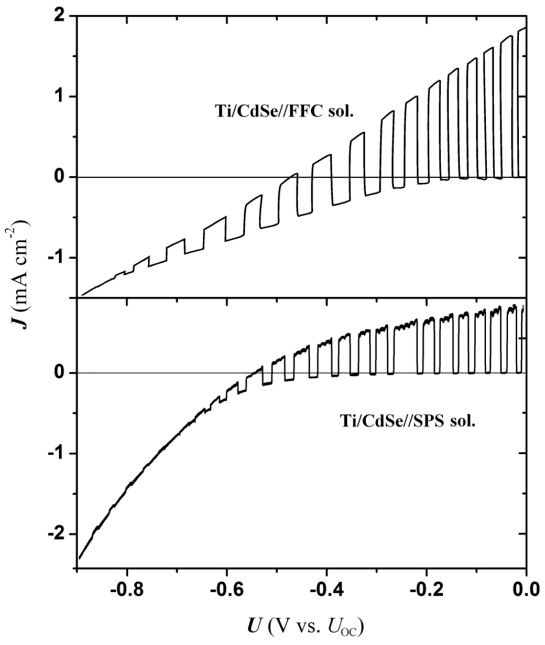
Figure 2.
Interface energetics for single crystal (sc) CdSe and polycrystalline (pc) CdSe/Ti electrodes in the respective electrolytes, according to the data of Table 1 (all values are quoted as V/SHE). The maximum band bending (EFB−ER/O) expected for each pc-CdSe//electrolyte system is indicated.
Figure 2.
Interface energetics for single crystal (sc) CdSe and polycrystalline (pc) CdSe/Ti electrodes in the respective electrolytes, according to the data of Table 1 (all values are quoted as V/SHE). The maximum band bending (EFB−ER/O) expected for each pc-CdSe//electrolyte system is indicated.
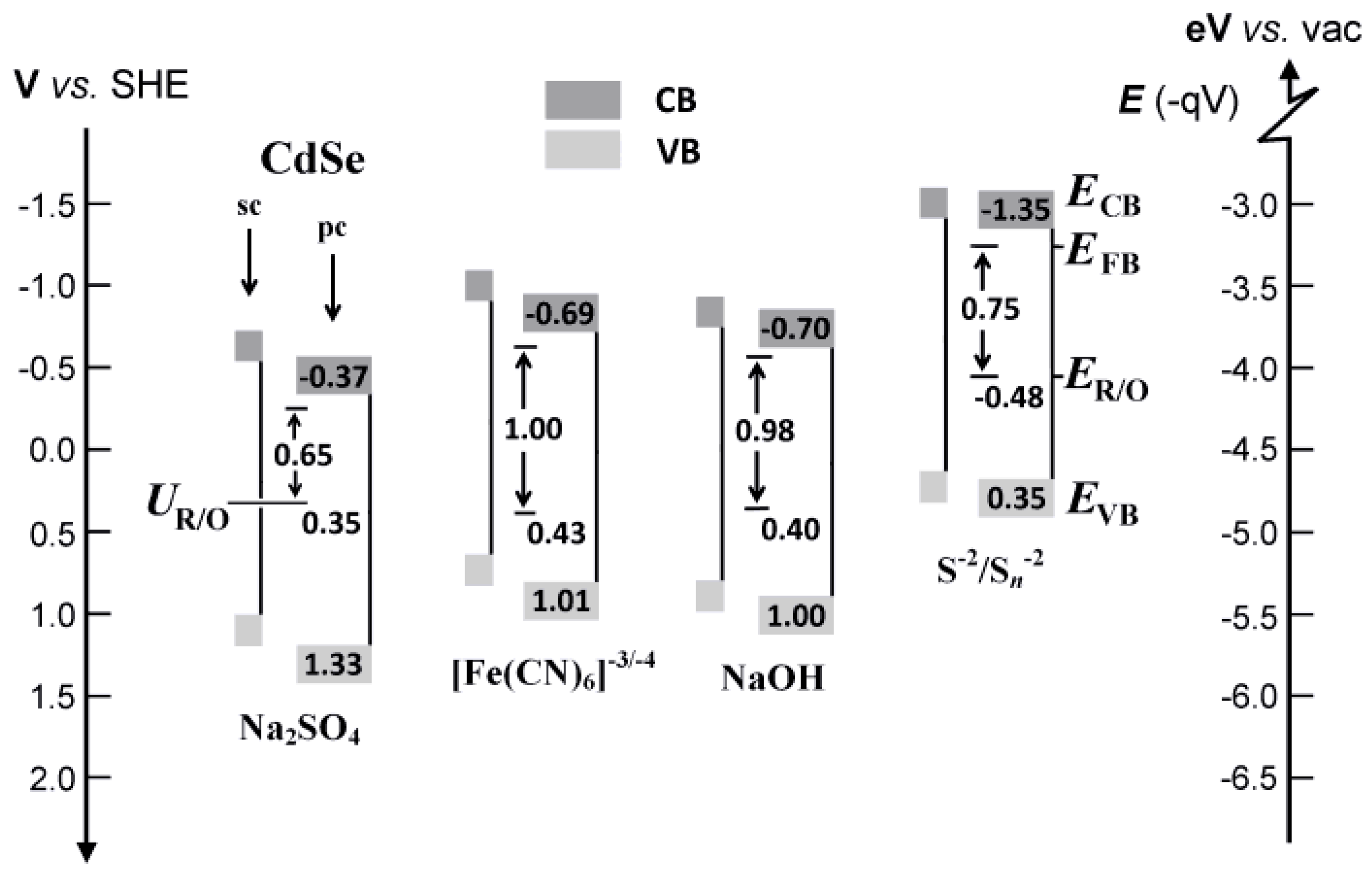
Figure 3.
Inverse square capacitance (C−2) vs. applied potential (U) for CdSe/(TiO2)Ti electrodes in contact with the SPS and FFC redox electrolytes and the respective NaOH and Na2SO4 (background) electrolytes: (a) in the dark; (b) under unit solar illumination. Impedance measurements performed at constant frequency 5 kHz; potential scan with 10 mV steps from 0.0 to −0.8 V.
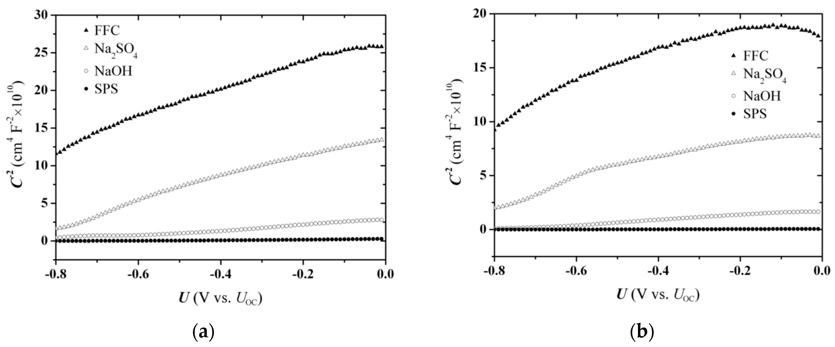
Figure 4.
C−2 vs. U plots for CdSe/TiO2 and CdSe/Ti electrodes in contact with SPS redox: (a) CdSe as-deposited; (b) CdSe annealed at 500 °C. Impedance measurements carried out in the dark at constant frequency 5 kHz and potential scan with 10 mV steps.
Figure 4.
C−2 vs. U plots for CdSe/TiO2 and CdSe/Ti electrodes in contact with SPS redox: (a) CdSe as-deposited; (b) CdSe annealed at 500 °C. Impedance measurements carried out in the dark at constant frequency 5 kHz and potential scan with 10 mV steps.
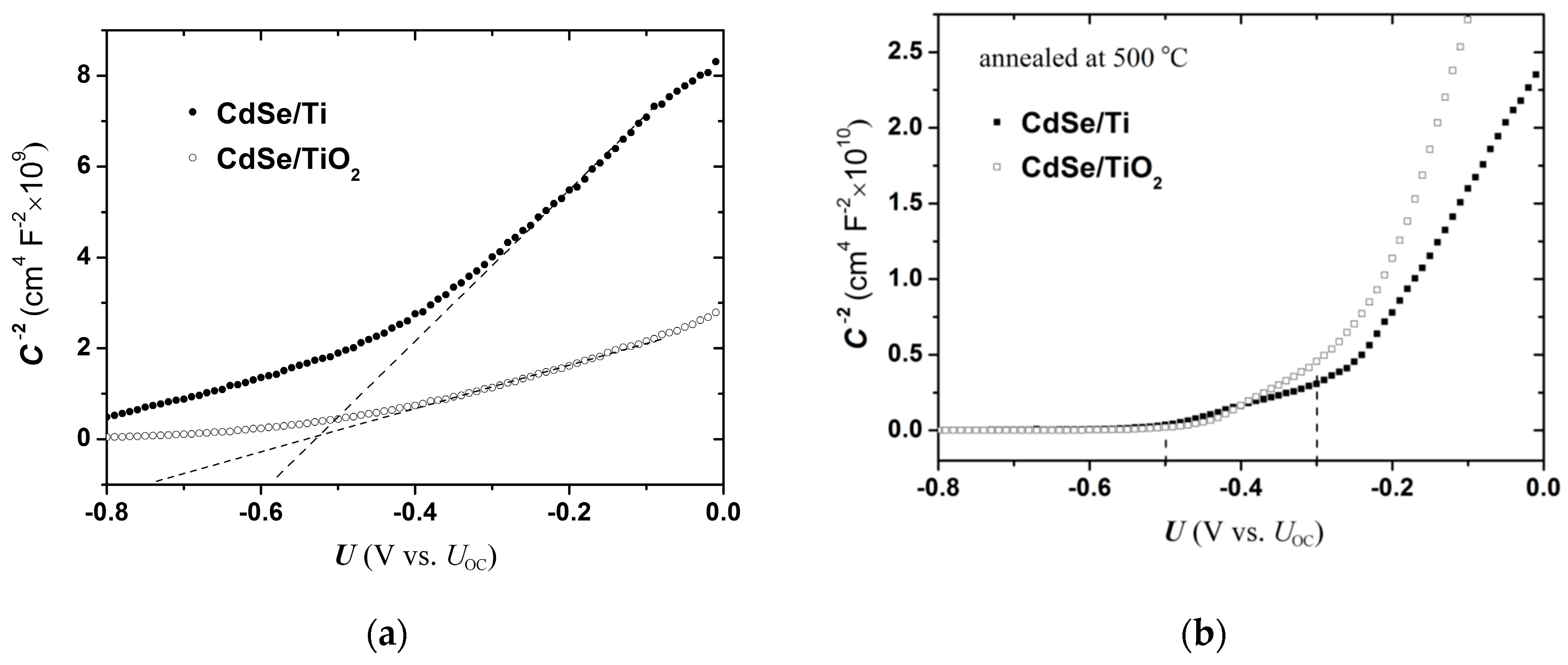
Figure 5.
Normalized C−2 vs. U for non-treated and annealed CdSe/Ti (a) and CdSe/TiO2 (b) electrodes, in contact with SPS redox. Impedance measurements carried out in the dark at constant frequency 5 kHz and potential scan with 10 mV steps.
Figure 5.
Normalized C−2 vs. U for non-treated and annealed CdSe/Ti (a) and CdSe/TiO2 (b) electrodes, in contact with SPS redox. Impedance measurements carried out in the dark at constant frequency 5 kHz and potential scan with 10 mV steps.
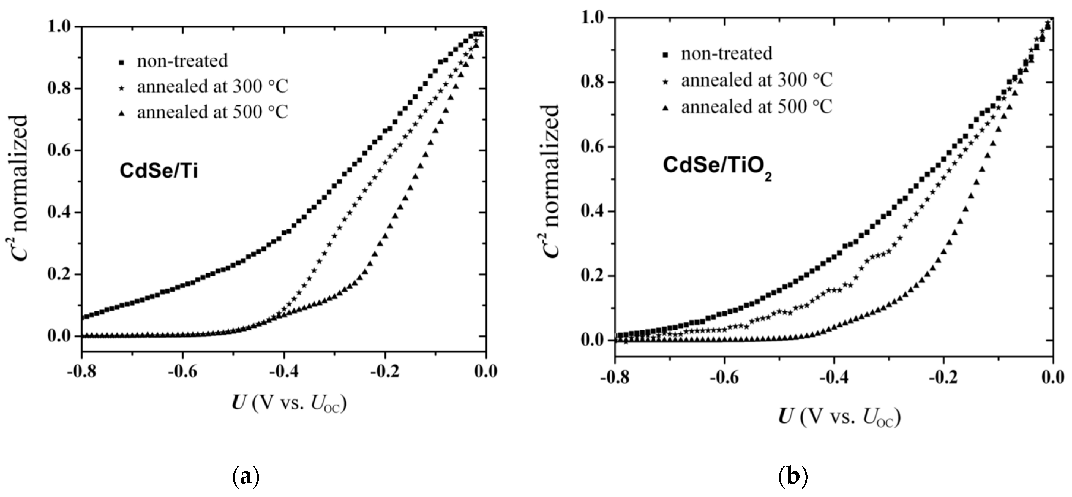
Figure 6.
Chopped-light photocurrent voltammetry for n-CdSe/Ti electrode annealed at 500 °C, in contact with SPS redox electrolyte (scan to the positive direction; rate 10 mV s−1). The photocurrent switch at ca. −0.50 V fades out with repetitive potential scans.
Figure 6.
Chopped-light photocurrent voltammetry for n-CdSe/Ti electrode annealed at 500 °C, in contact with SPS redox electrolyte (scan to the positive direction; rate 10 mV s−1). The photocurrent switch at ca. −0.50 V fades out with repetitive potential scans.
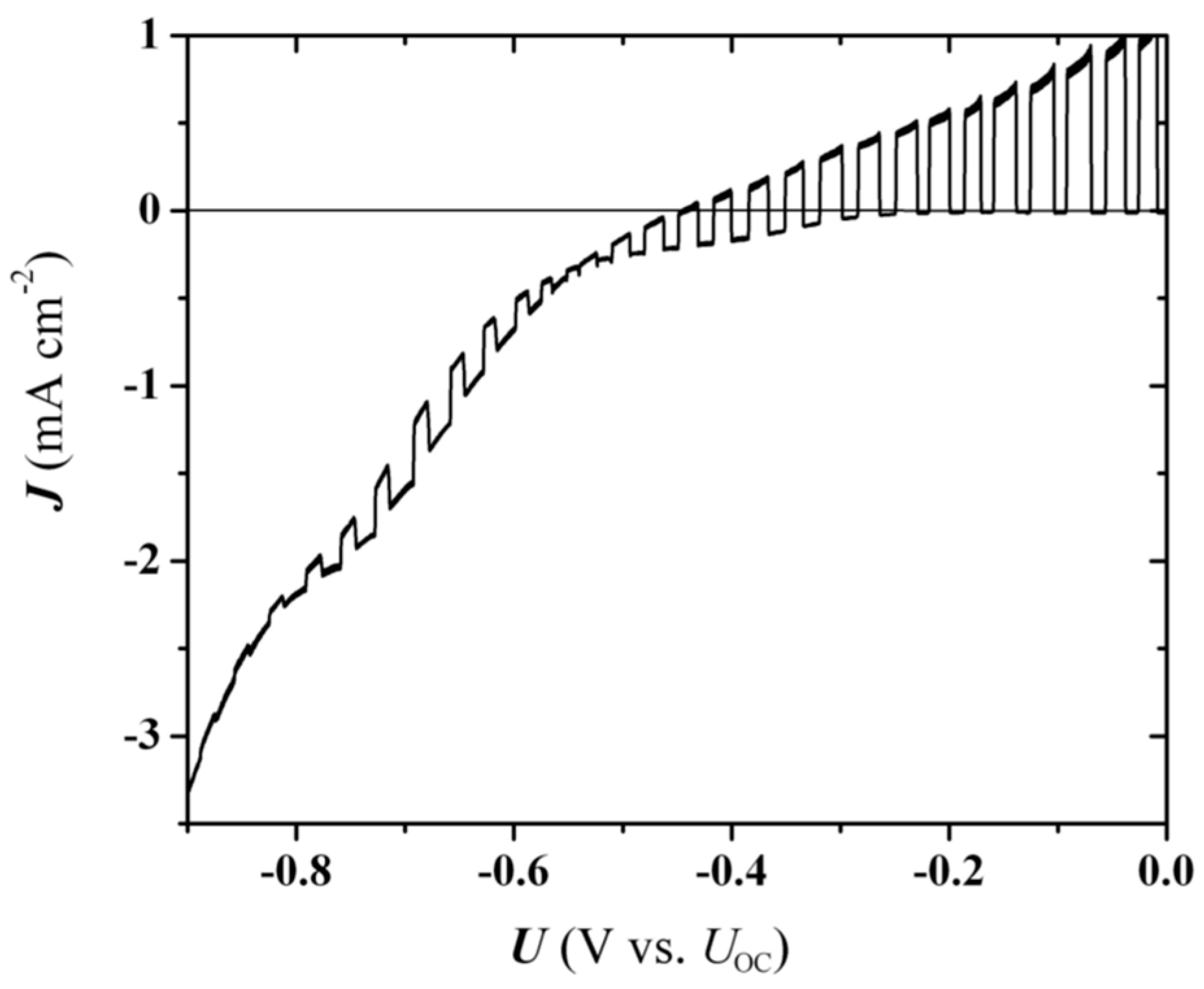
Figure 7.
C−2 vs. U plots for as-prepared CdSe/TiO2 electrodeposits in contact with the SPS redox solution in the dark. EI measurements were performed with successive scans of 10 mV steps at various constant frequencies, in the direction from higher to lower frequency.
Figure 7.
C−2 vs. U plots for as-prepared CdSe/TiO2 electrodeposits in contact with the SPS redox solution in the dark. EI measurements were performed with successive scans of 10 mV steps at various constant frequencies, in the direction from higher to lower frequency.
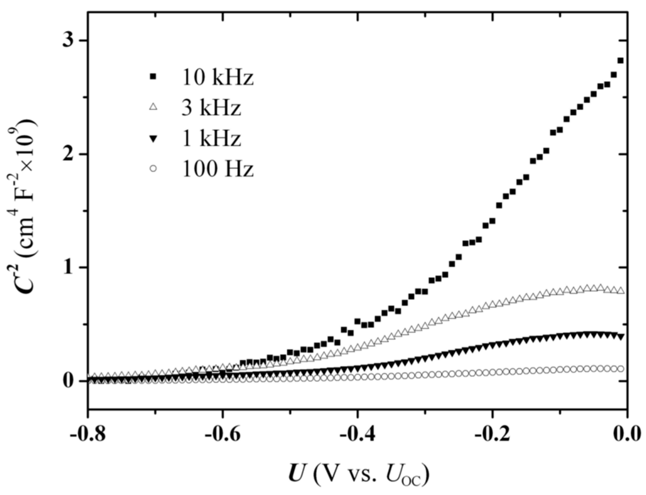
Figure 8.
C−2 vs. U plots of as-prepared CdSe/TiO2 electrodeposits in contact with the SPS redox solution in the dark. EI measurements were performed with successive scans of 50 mV steps at various constant frequencies, in the direction from higher to lower frequency.
Figure 8.
C−2 vs. U plots of as-prepared CdSe/TiO2 electrodeposits in contact with the SPS redox solution in the dark. EI measurements were performed with successive scans of 50 mV steps at various constant frequencies, in the direction from higher to lower frequency.
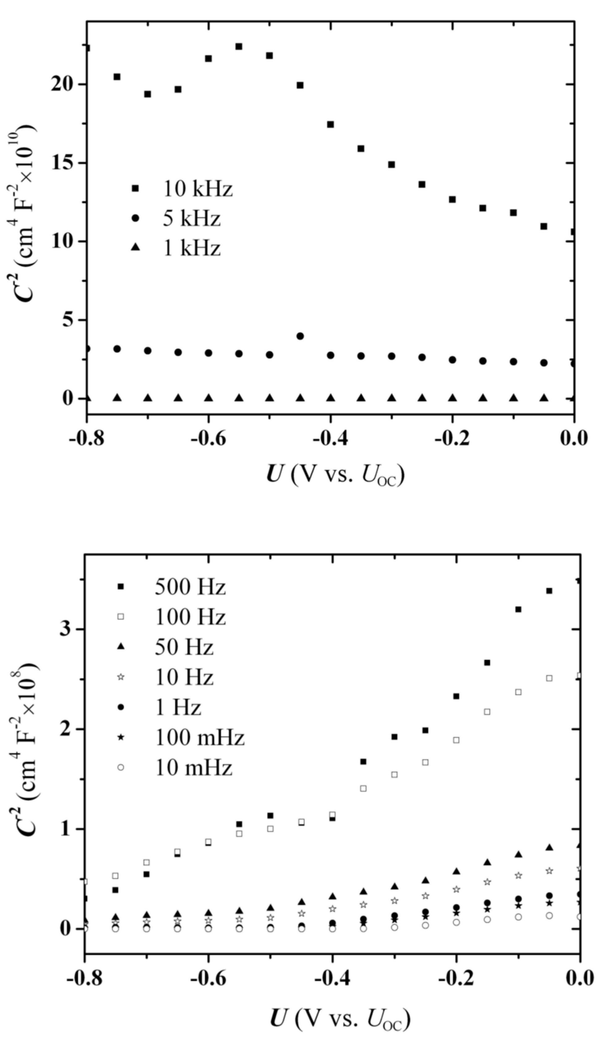
Figure 9.
C−2 vs. U plots of (a) TiO2/CdSe//Na2SO4; (b) Ti/CdSe//Na2SO4 and Ti/CdSe//NaOH electrodes. The electrodes were annealed at 300 °C. Impedance measurement performed under unit solar illumination at 5 kHz; potential scan with 10 mV steps.
Figure 9.
C−2 vs. U plots of (a) TiO2/CdSe//Na2SO4; (b) Ti/CdSe//Na2SO4 and Ti/CdSe//NaOH electrodes. The electrodes were annealed at 300 °C. Impedance measurement performed under unit solar illumination at 5 kHz; potential scan with 10 mV steps.
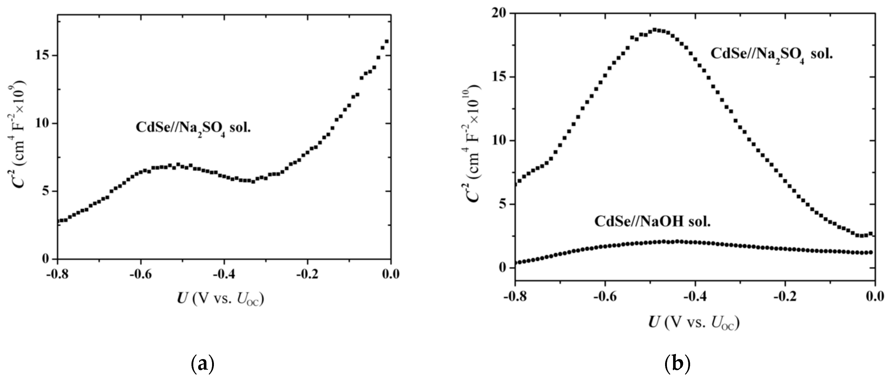
Figure 10.
Schematic of the C−2 vs. U graph evolution during successive scans towards the negative potentials, reflecting coverage of the electrode by a dielectric layer. In both diagrams, the dashed line 1 corresponds to the initial, uncoated electrode. In (a) complete surface covering occurs from scan 1 and gradually thinner layers are added after each scan (schematic above diagram). In case (b) partial surface covering of the electrode still holds after three scans.
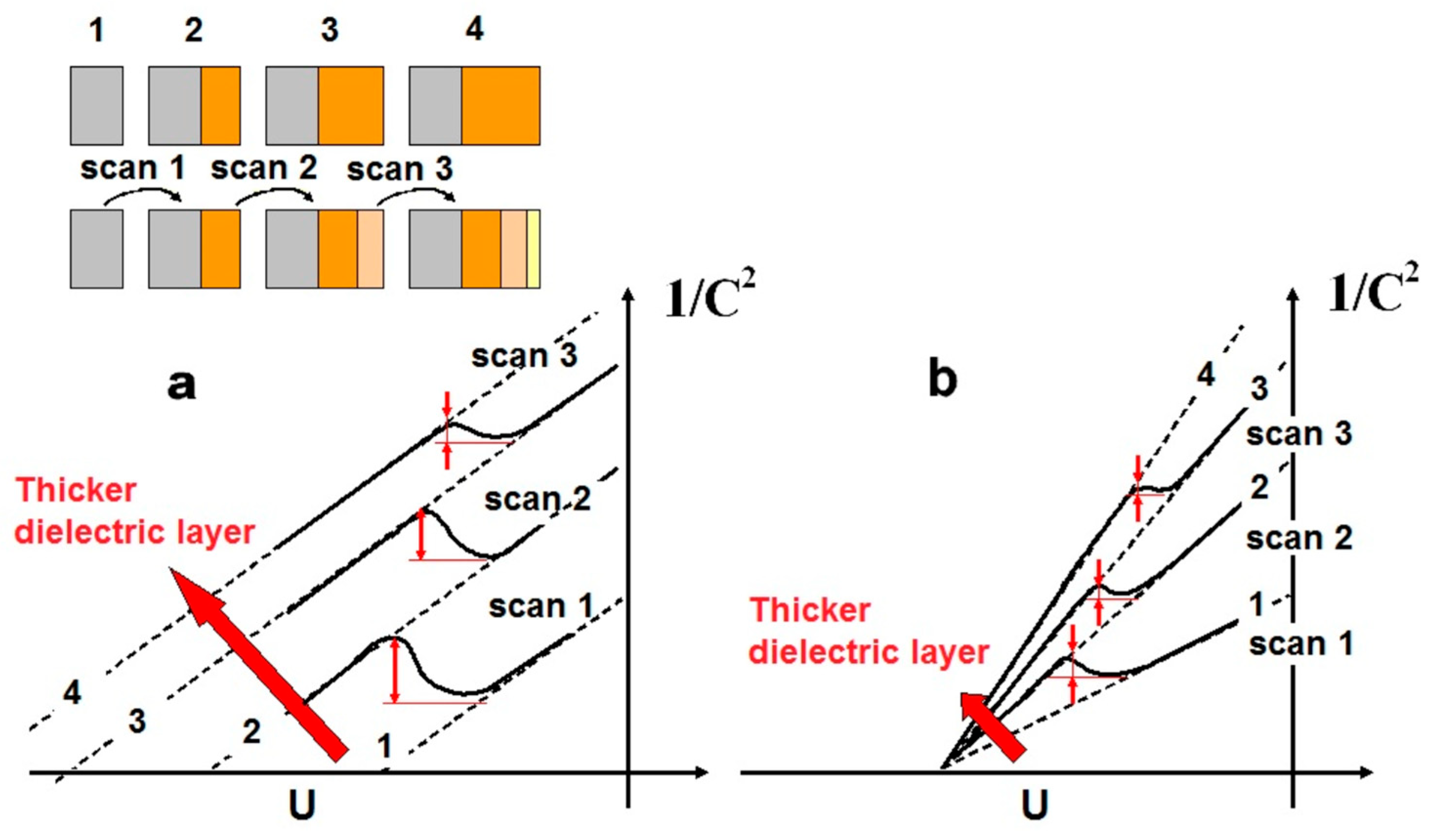

Table 1.
Redox potentials (UR/O) for the indicated electrolytes, along with flat band potentials (UFB) and band edge potentials (UCB, UVB) for single crystal n-CdSe (literature values; Lit.), and pc-CdSe/Ti (present measurements; Exp.) electrodes in each electrolyte. The exp. UR/O values are determined by cyclic voltammetry on Pt electrode vs Ag/AgCl. All values are given in V vs. SHE.
| Electrolyte Solution |
UR/O | UFB | UCB | UVB | ||||
|---|---|---|---|---|---|---|---|---|
| Lit. | Exp. | Lit. | Exp. | Lit. | Exp. | Lit. | Exp. | |
| 1 M Na2SO4 | 0.40 c | 0.35 | −0.48 c | −0.25 | −0.60 | −0.37 | 1.10 | 1.33 |
| 1 M NaOH | 0.40 | 0.40 | −0.71 b | −0.58 | −0.83 b | −0.70 | 0.87 | 1.0 |
| [Fe(CN)6]-3/-4 | 0.36 d, e | 0.43 | −0.72 d, e | −0.57 | −0.84 | −0.69 | 0.86 | 1.01 |
| S-2/Sn-2 | −0.48 a | −0.48 | −1.26 b | −1.23 | −1.38 b | −1.35 | 0.32 b | 0.35 |
Disclaimer/Publisher’s Note: The statements, opinions and data contained in all publications are solely those of the individual author(s) and contributor(s) and not of MDPI and/or the editor(s). MDPI and/or the editor(s) disclaim responsibility for any injury to people or property resulting from any ideas, methods, instructions or products referred to in the content. |
© 2026 by the authors. Licensee MDPI, Basel, Switzerland. This article is an open access article distributed under the terms and conditions of the Creative Commons Attribution (CC BY) license (http://creativecommons.org/licenses/by/4.0/).
Copyright: This open access article is published under a Creative Commons CC BY 4.0 license, which permit the free download, distribution, and reuse, provided that the author and preprint are cited in any reuse.


