Submitted:
13 February 2026
Posted:
14 February 2026
You are already at the latest version
Abstract
High-Al-content AlGaN microrods represent an effective platform for engineering deep-ultraviolet (DUV) emission. Here, we fabricated AlGaN microrods with varying diameters (2, 3, and 4 μm) via a top-down approach involving inductively coupled plasma dry etching followed by a KOH wet chemical modification. Their crystallographic facets and size-dependent optical properties were systematically investigated using scanning electron microscopy (SEM), cathodoluminescence (CL) spectroscopy, and CL mapping. We found that the KOH treatment selectively forms a-plane-dominated sidewalls on the high-Al-content portion of the microrods, whereas the etch pit bottoms stabilize as m-plane facets. Notably, the CL spectra show that the band-edge emission intensity of the 2-μm microrods is enhanced by a factor of 2.55 compared to the 4-μm structures. CL mapping further unveils the competitive dynamics between radiative recombination within the quantum wells and non-radiative recombination at surface states. These findings pinpoint 2 μm as a critical dimension for maximizing spontaneous emission from these high-Al-content AlGaN microrods.
Keywords:
AlGaN microrods
; deep-ultraviolet emission
; cathodoluminescence
; size effect
1. Introduction
AlGaN-based materials are pivotal for the development of deep-ultraviolet (DUV) optoelectronic devices for applications including sterilization, biochemical sensing, optical communication, and high-resolution lithography [1,2,3,4]. This is attributed to their direct and tunable wide bandgap, which covers the UVC spectral region. Nevertheless, the external quantum efficiency (EQE) of AlGaN-based DUV light-emitting devices remains disappointingly low compared to that of InGaN-based visible emitters, especially for wavelengths below 250 nm[5], which severely limits their practical applications.
Micro- and nanostructured architectures have emerged as a promising strategy to address these efficiency bottlenecks in III-nitride optoelectronics. Microrod structures, in particular, are advantageous due to their ability to facilitate strain relaxation, enhance light extraction, and control optical modes. The inherent large surface-to-volume ratio of microrods allows for effective strain relief, thereby suppressing the quantum-confined Stark effect (QCSE)[6]. Moreover, these structures function as optical microcavities, which can tailor the local photonic density of states and modulate spontaneous emission via the Purcell effect, ultimately improving the radiative recombination efficiency.
In the GaN-based material system, microrod and microdisk structures have demonstrated low-threshold lasing and effective confinement of whispering-gallery modes (WGMs) [7,8]. However, the extension of these microrod architectures to high-Al-content AlGaN systems for UVC emission is comparatively underdeveloped. Specifically, the intricate relationships connecting microrod morphology, crystallographic facet evolution, size-dependent optical phenomena, and defect-related emission in the DUV regime have yet to be systematically elucidated.
In this study, we fabricated AlGaN microrods with diameters of 2, 3, and 4 μm using a top-down approach that combines inductively coupled plasma (ICP) dry etching with a subsequent wet chemical treatment. Through a correlative analysis using detailed morphological characterization, cathodoluminescence (CL) spectroscopy, and CL mapping, we systematically investigated the relationships between crystallographic facet formation, size-dependent emission properties (intensity and linewidth), and spatial emission distribution. This work clarifies the critical roles of size confinement and surface-related effects in modulating UVC spontaneous emission, providing experimental insights to guide the design of high-performance AlGaN-based deep-ultraviolet optoelectronic devices.
2. Materials and Methods
2.1. Sample Preparation
The samples used in this study were fabricated from a standard AlGaN-based UVC LED epitaxial wafer grown on a sapphire substrate grown by metal–organic chemical vapor deposition (MOCVD). The epitaxial structure consists of a 3-μm-thick AlN layer, a 1.6-μm-thick n-Al0.62Ga0.38N layer, a 0.6-μm-thick n-Al0.35Ga0.65N layer, eight-period of Al0.8Ga0.2N/Al0.62Ga0.38N multiple quantum wells (MQWs), a 50 nm-thick p-Al0.88Ga0.12N EBL and a 50 nm-thick p-GaN layer.
The fabrication process of the AlGaN microrods is illustrated in Figure 1. Prior to patterning, the epitaxial wafer was immersed in diluted hydrochloric acid to remove surface oxides, followed by sequential ultrasonic cleaning in acetone, ethanol, and deionized water. A 500-nm-thick SiO2 layer was then deposited by plasma-enhanced chemical vapor deposition (PECVD). Positive photoresist (S1805) was spin-coated, and circular patterns with different diameters were defined by photolithography. A 30-nm-thick Ni film was deposited by electron-beam evaporation and subsequently lifted off in acetone to form circular Ni hard masks. Using the Ni disks as etching masks, the circular patterns were transferred into the SiO2 layer by inductively coupled plasma (ICP) etching. Subsequently, deep ICP etching was employed to transfer the defined patterns into the AlGaN epitaxial layers, forming microrods with well-controlled diameters. After dry etching, the remaining SiO2 layer was removed using buffered oxide etchant (BOE). To further eliminate etching-induced surface damage and improve sidewall quality, the samples were subjected to wet chemical treatment in a 2 mol/L KOH solution heated to 80 °C for 10 min. Through this combined dry and wet etching process, AlGaN microrods with diameters of 2 μm, 3 μm, and 4 μm were obtained.
2.2. Structural and Optical Characterization
High-resolution X-ray diffraction (HR-XRD) was employed to characterize the crystallographic orientations of the AlGaN microrods. The sidewall morphologies were examined using scanning electron microscopy (SEM). Cathodoluminescence (CL) spectroscopy and CL mapping were performed to investigate the optical emission properties.
CL measurements were conducted at an electron beam acceleration voltage of 12 kV with a beam current of approximately 5 nA. The excitation mode was point excitation, with an electron beam spot size of approximately 20 nm and an integration time of 2 s. Multiple microrods with different diameters were measured under identical conditions to ensure reliable comparison. Spatially resolved CL mapping was further carried out to obtain two-dimensional emission distributions, local spectra, and quantitative parameters, including emission intensity, peak position, and full width at half maximum (FWHM). The working distance was set to 9.3 mm to achieve sufficient spatial resolution for resolving emission variations across the microrods.
3. Results and Discussion
3.1. Morphological Analysis
To determine the crystallographic orientations of the sidewalls and etching pits in the AlGaN microrods, X-ray diffraction (XRD) φ-scan measurements of the r-plane were performed. Within a scanning range of 180°, diffraction peaks appeared at 60° intervals, originating from the sixfold symmetry of the wurtzite crystal structure. By rotating the sample to one diffraction peak position, the horizontal cross-sectional direction was aligned with the m-plane, followed by side-view observations using scanning electron microscopy (SEM).
Figure 2 shows the side-view SEM images of the AlGaN microrods. Before KOH treatment, the microrod is a lithographically defined cylinder, and the sidewalls show roughness caused by ICP etching, as shown in Figure 2a. After treatment with KOH, the microrod exhibited a prismatic structure of specific crystal planes as shown in Figure 2b. In the high-Al-content AlGaN region of the microrod, the sidewalls form an angle of approximately 30° with respect to the m-plane direction, while the bottom facets of the etching pits remain parallel to the m-plane. Based on the geometrical relationships among crystallographic planes in the wurtzite structure, the sidewalls are identified as a-planes, whereas the bottom facets correspond to m-planes.
Figure 2b show that following KOH treatment, the sidewalls become smoother and evolve into stable facets dominated by a-planes, while the etching pits expand outward and stabilize as m-plane–related semipolar facets. After KOH treatment, it is very unusual for high Al-content components to spontaneously exhibit the a-plane. In numerous past studies, it has been found that for GaN-based materials, the crystal plane that spontaneously appears after KOH treatment is always the m-plane[9,10,11]. Therefore, AlN and materials with high Al content have crystal plane characteristics different from those of GaN. The top part of the microrod is made of low-Al-content AlGaN and GaN, so it still tends to form m-planes. However, because the thickness of this part is too small, it ultimately appears nearly circular.
This facet-selective etching behavior can be attributed to differences in atomic configurations between nonpolar planes. For AlN, the surface atomic density of the a-plane (0.745 Å⁻²) is higher than that of the m-plane (0.645 Å⁻²), resulting in greater chemical stability of the a-plane[12]. In alkaline KOH solution, negatively charged OH⁻ ions experience stronger electrostatic repulsion near the a-plane family, whereas the repulsion is weaker near the m-plane family. As a result, m-plane–related facets are preferentially etched during wet chemical treatment, while a-plane facets tend to be preserved. Consequently, the microrod sidewalls are dominated by a-plane facets with minor residual ridges originating from m-plane segments, whereas the bottom etching pits preferentially expose m-plane–related facets during outward etching.
The observed facet evolution behavior is consistent with previous reports on top-down fabricated GaN and AlN micro- and nanostructures. Similar facet selectivity, featuring a-plane or a-plane–related semipolar sidewalls and m-plane–dominated bottom facets, has been reported in high-aspect-ratio GaN/AlN nanopillars fabricated by combined dry and wet etching processes[13,14,15]. In addition, ultrasharp periodic AlN nanotips fabricated by thinning processes also exhibit a-plane–related semipolar sidewalls with an angle of approximately 30° relative to the m-plane at the bottom facets[16]. These results indicate that facet separation toward a-plane and m-plane families during wet chemical etching is highly dependent on the Al component in the wurtzite III-nitride materials.
Figure 3 presents SEM images of microrods with diameters (D) of 2 μm, 3 μm, and 4 μm, and exhibit consistent facet characteristics. The lower half of the high-alumina component in all microrods exhibits a clear a-face, while the crystal face features of the upper half of the low-alumina component gradually disappear.
Overall, the microrod morphology is governed by both etching conditions and intrinsic crystallographic properties. The formation of a-plane sidewalls provides a well-defined structure for the size-dependent optical properties discussed below.
3.2. Point Spectral Analysis
The size-dependent optical properties were investigated by performing point-excitation CL spectra from individual AlGaN microrods with diameters of 2, 3, and 4 μm, as presented in Figure 4. To elucidate the underlying recombination dynamics, spectra were recorded at three distinct excitation currents, 5.0, 0.5, and 0.05 nA, corresponding to relative power densities of P, 0.1P, and 0.01P, respectively, while maintaining identical collection conditions.
The representative spectra in Figure 4a and Figure 4c, and 4e consistently reveal three distinct emission peaks for all microrods. The dominant feature is a DUV emission centered at ~250 nm, which is accompanied by a shoulder-like feature at ~290 nm and a broad blue luminescence band near 440 nm. Crucially, the evolution of these bands with increasing excitation power is markedly different, indicating that they come from different recombination.
Figure 4b and Figure 4d, and 4f summarize the normalized emission intensities as a function of microrod diameter. The 250 nm emission intensity increases significantly with decreasing microrod diameter and displays a superlinear dependence on excitation power. The 290 nm emission follows a similar size-dependent trend, although the enhancement is less pronounced. Based on their spectral positions, we attribute the 250 nm peak to band-edge recombination within the MQWs. In contrast, the 290 nm peak is assigned to recombination in the lower-Al-content AlGaN layer, likely following carrier diffusion out of the QWs.
In contrast, the 440 nm emission displays a weak dependence on excitation power and exhibits clear saturation at higher levels. This behavior is characteristic of recombination by deep-level defects. In AlGaN, this blue luminescence is widely attributed to carbon-related defects (such as C-N), which serve as radiative recombination centers[17,18].
To deconvolve the spectral components, the CL spectrum of a representative microrod was fitted using a multi-peak Gaussian function (Figure 5). The analysis yields three distinct peaks, labeled A, B, and C. These peaks are assigned to band-edge recombination in the MQWs (A), the lower-Al-content AlGaN layer (B), and carbon-related deep-level defects (C), respectively. The extracted center wavelengths for each peak are consistent with these physical assignments.
The evolution of the band-edge emission FWHM with excitation power reveals distinct differences in carrier recombination dynamics between the microrods (Figure 6(a)). The 4-µm microrod displays a consistently narrow FWHM, indicating a high degree of material homogeneity. Conversely, the 2-µm microrod exhibits a significantly broader FWHM at low excitation, which progressively narrows at higher powers.
This behavior is explained by the magnified role of surface states in structures with a high surface-to-volume ratio. These surface states create a broad distribution of energy levels that act as alternative recombination pathways. At low carrier densities, recombination occurs across this wide energy landscape, resulting in significant spectral broadening. However, under high excitation, the system undergoes a state-filling effect: the more efficient, intrinsic band-edge recombination channel becomes saturated with carriers and dominates the emission spectrum. This saturation diminishes the relative contribution of the broader surface-state recombination, leading to the pronounced line-narrowing observed in the 2-μm microrod.
A strong enhancement in band-edge emission intensity is also observed as the microrod diameter decreases (Figure 6b). Under identical excitation conditions, the integrated intensity from the 2 µm microrods is 2.55 times greater than that from the 4 µm structures. This intensity boost is a key signature of the Purcell effect, where the optical cavity formed by the microrod increases the spontaneous emission rate. By accelerating radiative recombination, the cavity allows emission to more effectively compete with non-radiative processes, thereby boosting the overall light output. The previously discussed line-narrowing behavior further supports this conclusion, as the Purcell effect selectively enhances the primary band-edge recombination channel that comes to dominate the spectrum at high power.[19].
3.3. Spatially Resolved Spectral Analysis
To directly visualize the impact of surface recombination, we performed spatially resolved cathodoluminescence (CL) mapping. The monochromatic maps, taken at the 250 nm band-edge emission, reveal a luminescent core surrounded by a non-radiative "dead layer" at the microrod perimeter (Figure 7). This dead layer represents the region where charge carriers are depleted by rapid non-radiative recombination at the surface states.
Furthermore, the width of this dead layer exhibits a strong dependence on the microrod diameter. As summarized in Figure 8, the dead layer width increases with diameter before beginning to saturate. This trend is governed by carrier diffusion: in larger microrods, carriers generated deeper within the core can diffuse a greater distance before reaching the surface, resulting in a wider apparent region of suppressed emission near the edge.
This size-dependent behavior is governed by a competition between two key processes: radiative recombination within the quantum wells and non-radiative recombination at the etched sidewalls. In smaller microrods, the small diameter provides stronger strain relaxation. This reduces band bending near the microrod edge suppressing electron diffusion toward the sidewalls s [20], and the quantum-confined Stark effect (QCSE) leading to greater electron-hole wavefunction overlap and a higher radiative recombination rate. As a result, carriers recombine radiatively before they can diffuse to the surface, resulting in a narrower non-emissive "dead layer."
Conversely, in larger microrods, strain relaxation is less complete. The stronger QCSE suppresses radiative efficiency, increasing the carrier lifetime. This provides more time for carriers to diffuse laterally toward the sidewalls, where they are captured by etch-induced defect states and recombine non-radiatively. The dead layer width therefore increases with diameter. However, this width is ultimately limited by the carrier diffusion length, explaining the slower increase observed for the largest microrods (Figure 8).
To identify the source of the non-radiative regions, we compared the spatial distribution of the band-edge emission with that of the defect-related luminescence (Figure 9). The maps reveal a clear anti-correlation: the bright band-edge emission is concentrated in the microrod core, while the defect emission is also dominant at the perimeter, spatially coinciding with the non-emissive "dead layer."
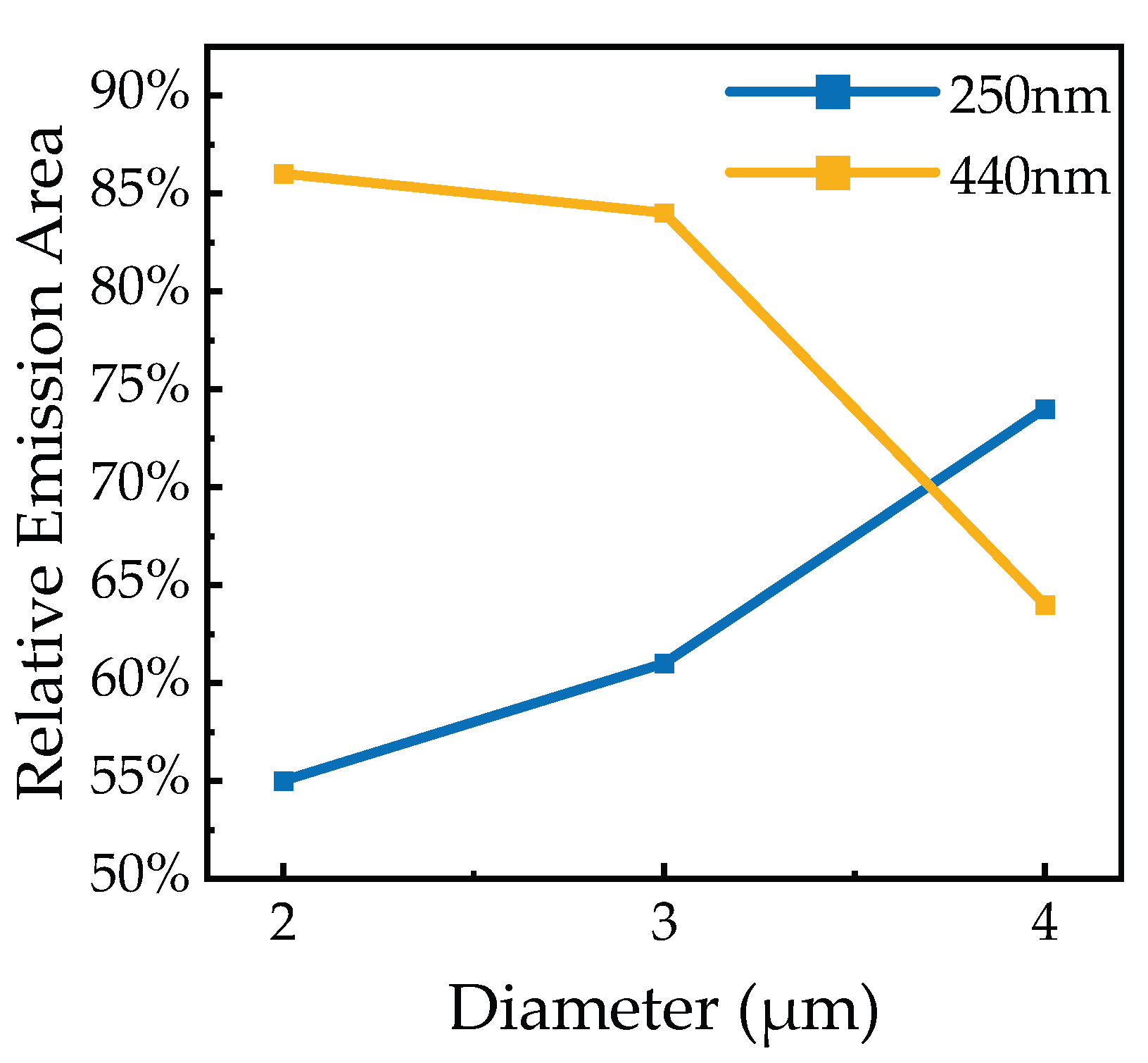
This spatial competition is quantified in Figure 10. As the microrod diameter increases from 2 µm to 4 µm, the fractional area of band-edge emission grows significantly from 55% to 74%. Concurrently, the area dominated by defect-related emission shrinks from 86% to 64%. At this point, an interesting pattern can be observed: although the band-edge emission volume ratio in small-sized microrods is smaller than that in large-sized microrods, the overall band-edge emission intensity is stronger (as seen in Figure 6b), which demonstrates a change in the radiative mechanism in the small-sized microrods.
Overall, the 2-µm AlGaN microrods emerge as the optimal structure, exhibiting superior band-edge emission intensity, excitation-induced linewidth narrowing, and distinct spatial emission. This peak performance arises from a synergy between two size-dependent effects. First, like other smaller microrods, they benefit from significant strain relaxation, which suppresses the QCSE and enhances intrinsic radiative recombination. Crucially, however, it is at the 2-µm diameter that the Purcell effect becomes most pronounced, further accelerating spontaneous emission. This combined enhancement of both radiative efficiency and emission rate defines 2 µm as a critical dimension for tailoring the optical properties of AlGaN microrod structures.
4. Conclusions
In summary, the facet evolution and size-dependent emission behavior of AlGaN microrods fabricated by dry etching followed by KOH wet chemical modification were investigated. We found that the KOH treatment preferentially forms a-plane-dominated sidewalls on the high-Al-content regions of the microrods, whereas the etch pit bottoms stabilize as m-plane facets. Optical characterization reveals smaller microrods exhibiting enhanced band-edge emission and excitation-dependent linewidth narrowing. In particular, the band-edge emission intensity of the 2-μm microrods is enhanced by a factor of 2.55 compared to the 4-μm structures. CL mapping further unveils the competitive dynamics between radiative recombination within the quantum wells and non-radiative recombination at surface states. These results identify 2 μm as a critical dimension for maximizing spontaneous emission in AlGaN microrods and emphasize the importance of facet engineering and size confinement in designing high-performance deep-ultraviolet optoelectronic devices.
Author Contributions
Conceptualization, P.C.; methodology, X.S., T.X. and Z.Y.; software, X.S., J.Z. and Z.Y.; investigation, X.S. and P.C.; formal analysis P.C.; resources, P.C., Z.X., D.C., Y.S., R.Z. and Y.Z.; data curation, X.S.; writing—original draft preparation, X.S.; writing—review and editing, P.C.; supervision, Y.S., R.Z. and Y.Z; Funding acquisition, P.C. All authors have read and agreed to the published version of the manuscript.
Funding
This work is supported by National Key Research and Development Program of China (2024YFE0204600).
Data Availability Statement
All data, theory detail that support the findings of this study are available from the corresponding authors upon reasonable request.
Acknowledgments
The authors acknowledge Jiangsu Provincial Key Laboratory of Advanced Photonic and Electronic Materials, State Key Laboratory of Spintronics and Nanjing University for their support in advanced microtechnology and clean room facilities.
Conflicts of Interest
The authors declare no conflict of interest.
References
- Chatterley, Christie; Linden, Karl. Demonstration and evaluation of germicidal UV-LEDs for point-of-use water disinfection. Journal of Water and Health 2010, 8, 479–486. [Google Scholar] [CrossRef] [PubMed]
- Mahajan, Sumeet. Mechanisms of SARS-CoV-2 Inactivation Using UVC Laser Radiation. ACS Photonics 2024, 11, 42–52. [Google Scholar]
- Ponce, F. A.; Bour, D. P. Nitride-based semiconductors for blue and green light-emitting devices. Nature 1997, 386, 351–359. [Google Scholar] [CrossRef]
- Taniyasu, Y.; Kasu, M.; Makimoto, T. An aluminium nitride light-emitting diode with a wavelength of 210 nanometres. Nature 2006, 441, 325–328. [Google Scholar] [CrossRef] [PubMed]
- Zhang, C Y; Jiang, K; Sun, X J; et al. Recent Progress on AlGaN Based Deep Ultraviolet Light-Emitting Diodes below 250 nm. Crystals 2022, 12, 1812. [Google Scholar] [CrossRef]
- Leung, B. Y.; et al. Strain relaxation and dislocation reduction in AlGaN step-graded buffer for crack-free GaN on Si (111). Physica Status Solidi (c) 2014, 11, 610–613. [Google Scholar] [CrossRef]
- Li, Yuyin; Chen, Peng; Zhang, Xianfei. The Study on the Lasing Modes Modulated by the Dislocation Distribution in the GaN-Based Microrod Cavities. Nanomaterials 2023, 13, 2228. [Google Scholar] [CrossRef] [PubMed]
- Li, Yuyin; Zhou, Jing; Chen, Peng. GaN microdisks with a single porous optical confinement layer for whispering gallery mode lasing. Appl. Phys. Lett 2024, 125, 093504. [Google Scholar] [CrossRef]
- Zhuang, D; Edgar, J H. Wet etching of GaN, AlN, and SiC: a review. Materials Science and Engineering: R: Reports 2005, 48, 1–46. [Google Scholar] [CrossRef]
- Seitz, M; Boisvere, J; Melanson, B; Morrell, JW; Manimaran, NH; Xu, K; Zhang, J. Analytical study of KOH wet etch surface passivation for III-nitride micropillars. iScience 2024, 27, 109423. [Google Scholar] [CrossRef] [PubMed]
- Hartensveld, Matthew; Ouin, Gildas; Liu, Cheng; Zhang, Jing. Effect of KOH passivation for top-down fabricated InGaN nanowire light emitting diodes. J. Appl. Phys. 2019, 126, 183102. [Google Scholar] [CrossRef]
- Leathersich, Jeff; et al. Homoepitaxial growth of non-polar AlN crystals using molecular dynamics simulations. Surface Science 2013, 616, 195–201. [Google Scholar] [CrossRef]
- Coulon, P M; Kusch, G; Fletcher, P; et al. Hybrid top-down/bottom-up fabrication of a highly uniform and organized faceted AlN nanorod scaffold. Materials 2018, 11, 1140. [Google Scholar] [CrossRef] [PubMed]
- Jaloustre, L; De Mello, S S; Labau, S. Faceting mechanisms of GaN nanopillar under KOH wet etching. Materials Science in Semiconductor Processing 2024, 173, 108095. [Google Scholar] [CrossRef]
- Kazanowska, Barbara A.; et al. Fabrication and field emission properties of vertical, tapered GaN nanowires etched via phosphoric acid. Nanotechnology 2022, 33, 035301. [Google Scholar] [CrossRef] [PubMed]
- Armstrong, R F; Shields, P A. Ultrasharp periodic AlN nanotips formed via purely subtractive nanofabrication. Microelectronic Engineering 2025, 298, 112312. [Google Scholar] [CrossRef]
- Xie, Z; Sui, Y; Buckeridge, J. Assignment of multiband luminescence due to the gallium vacancy–oxygen defect complex in GaN. Applied Physics Letters 2018, 112, 262104. [Google Scholar] [CrossRef]
- Reshchikov, M A. Fine Structure of the Carbon-Related Blue Luminescence Band in GaN. Solids 2022, 3, 231–236. [Google Scholar] [CrossRef]
- Purcell, E M. Spontaneous emission probabilities at radio frequencies. Physical Review 1946, 69, 681. [Google Scholar]
- Jiang, C R; Moniz, S J A; Wang, A Q; et al. Photoelectrochemical devices for solar water splitting-materials and challenges. Chemical Society Reviews 2017, 46, 4645–4660. [Google Scholar] [CrossRef] [PubMed]
Figure 1.
Fabrication process of the microrod cavities. The original epitaxial wafer (a), the SiO2 deposition (b), the Ni hard mask formed by photolithography and lift-off (c), etching of SiO2(d), inductively coupled plasma itching of the wafer (e), and removal of the SiO2(f).
Figure 1.
Fabrication process of the microrod cavities. The original epitaxial wafer (a), the SiO2 deposition (b), the Ni hard mask formed by photolithography and lift-off (c), etching of SiO2(d), inductively coupled plasma itching of the wafer (e), and removal of the SiO2(f).
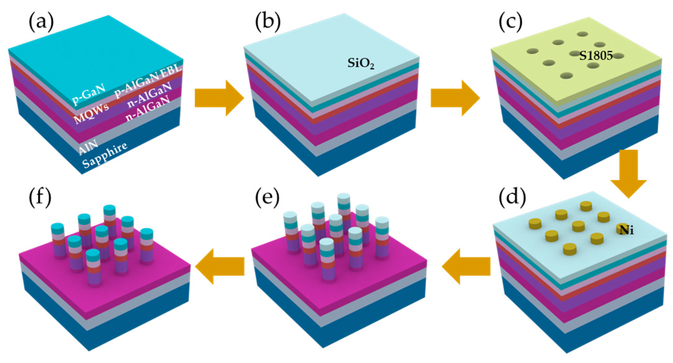
Figure 2.
SEM side-view images of AlGaN microrod (a) before and (b) after modification. The scale bars represent 2 μm.
Figure 2.
SEM side-view images of AlGaN microrod (a) before and (b) after modification. The scale bars represent 2 μm.
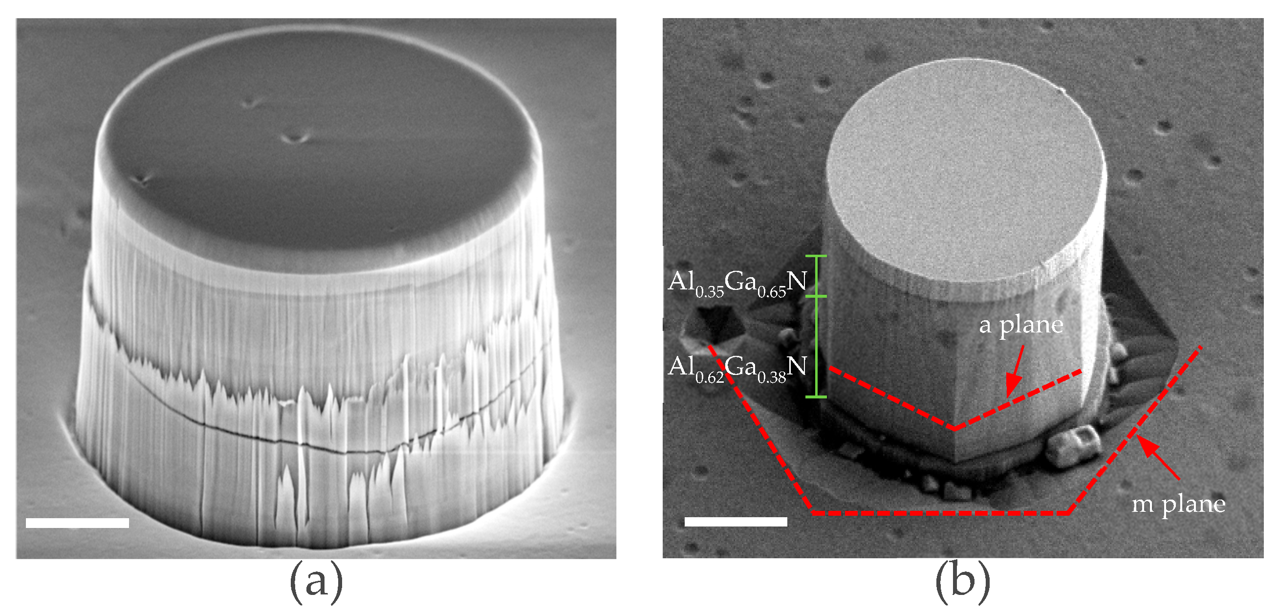
Figure 3.
SEM side-view images of microrods with different sizes. The scale bars represent 1 μm.
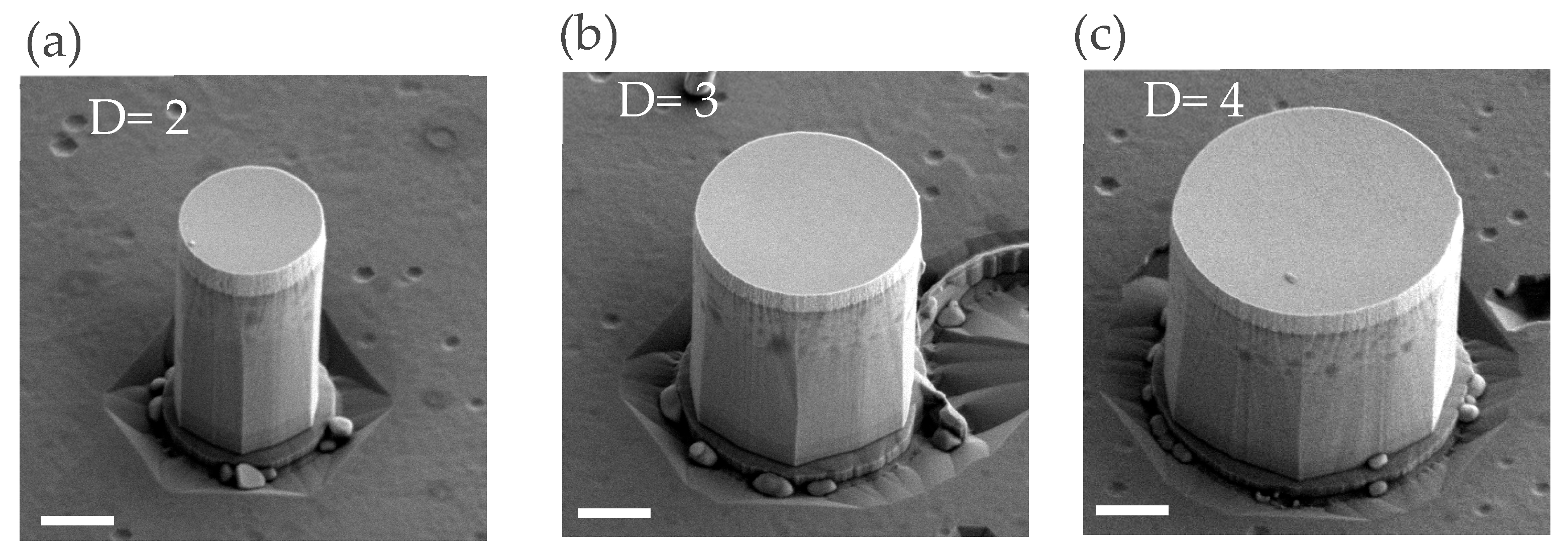
Figure 4.
CL from (a) 2 μm, (c) 3 μm, (e) 4 μm microrod. The dependence of CL peak intensity on excitation power is shown in (b, d, f) for each emission peak.
Figure 4.
CL from (a) 2 μm, (c) 3 μm, (e) 4 μm microrod. The dependence of CL peak intensity on excitation power is shown in (b, d, f) for each emission peak.
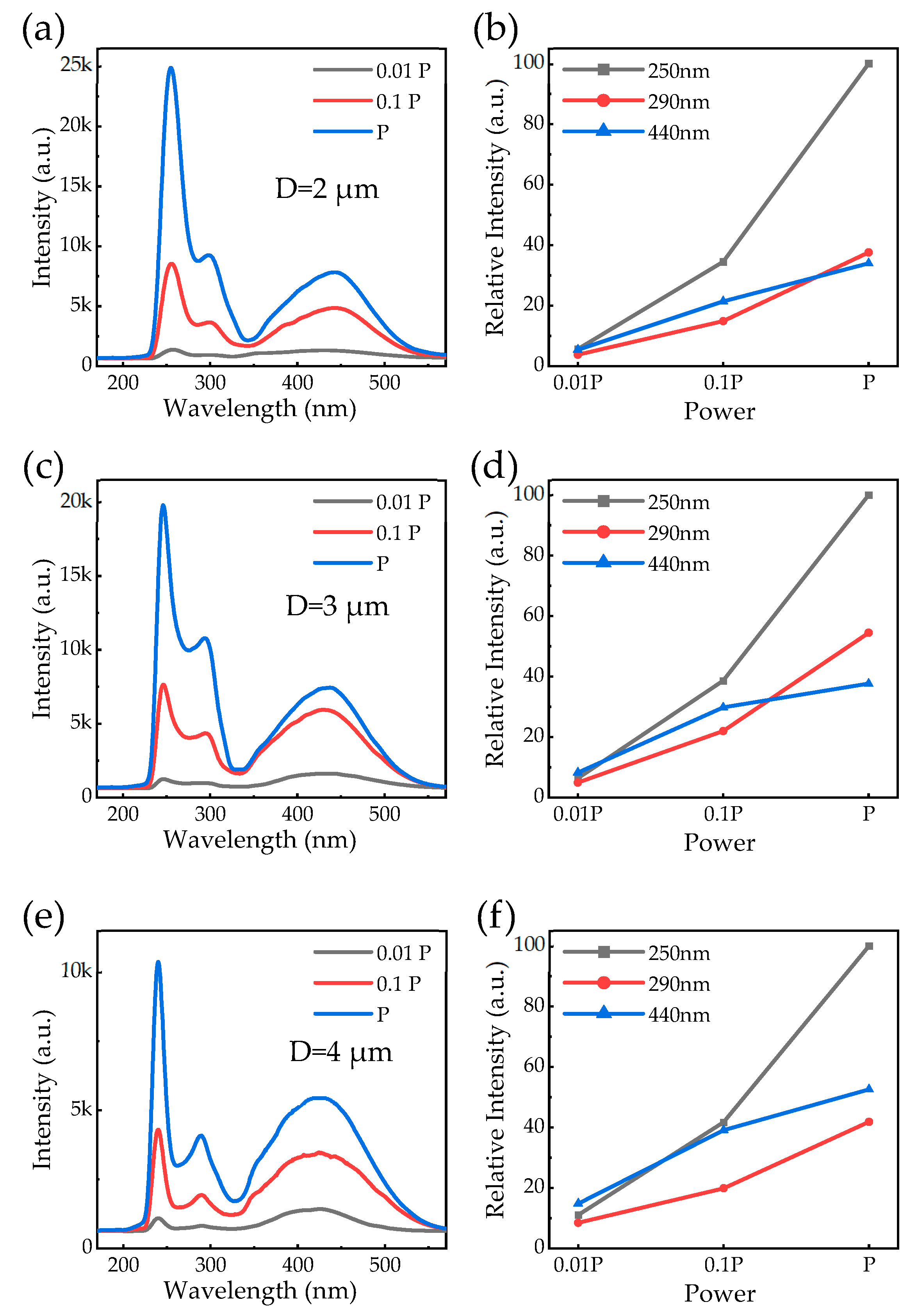
Figure 5.
Gaussian fitting of the CL spectrum of 2-μm-diameter AlGaN microrod (a) and band-edge emission peak (b).
Figure 5.
Gaussian fitting of the CL spectrum of 2-μm-diameter AlGaN microrod (a) and band-edge emission peak (b).
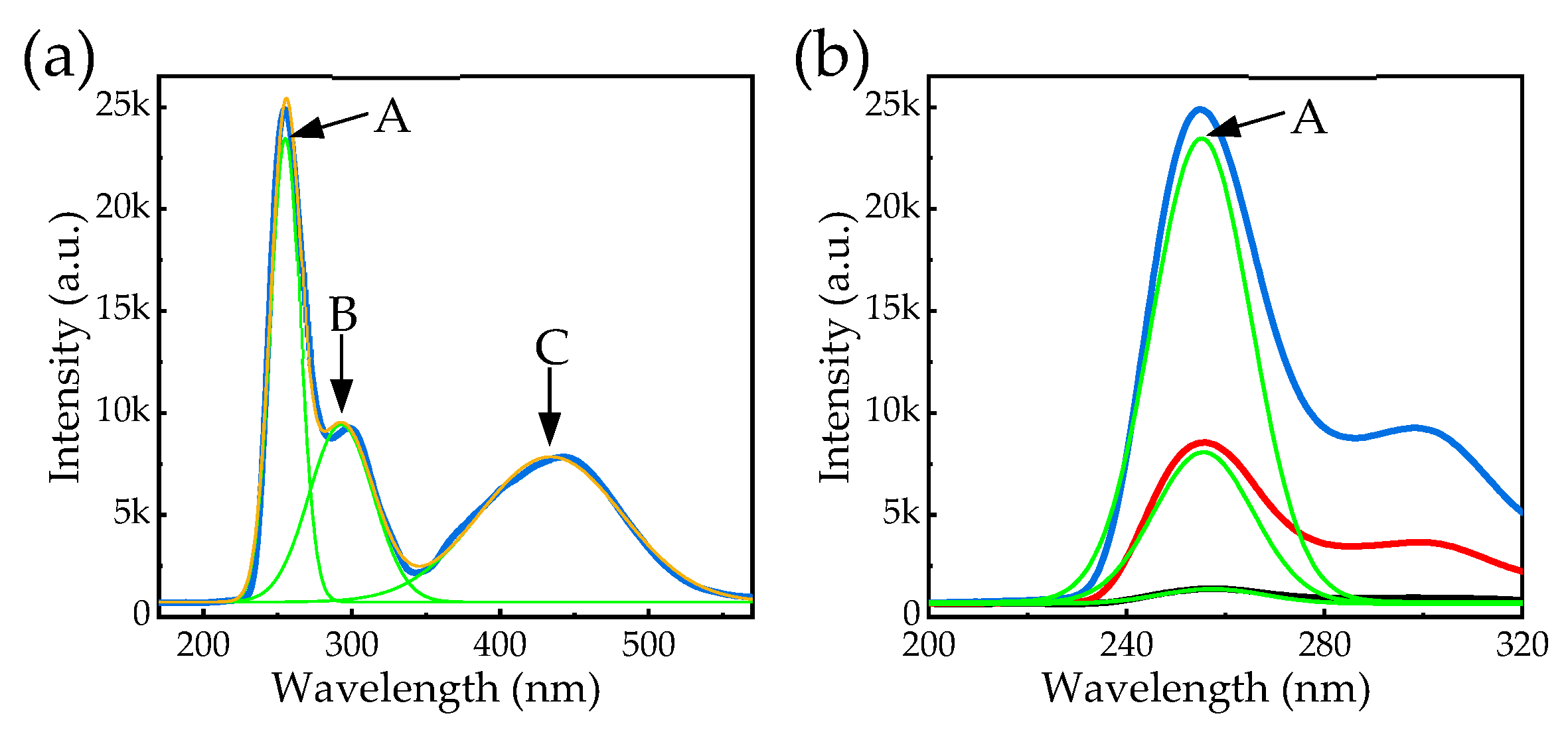
Figure 6.
Variation of FWHM for samples of different sizes (a) and variation of the peak intensity of the band-edge emission (b).
Figure 6.
Variation of FWHM for samples of different sizes (a) and variation of the peak intensity of the band-edge emission (b).
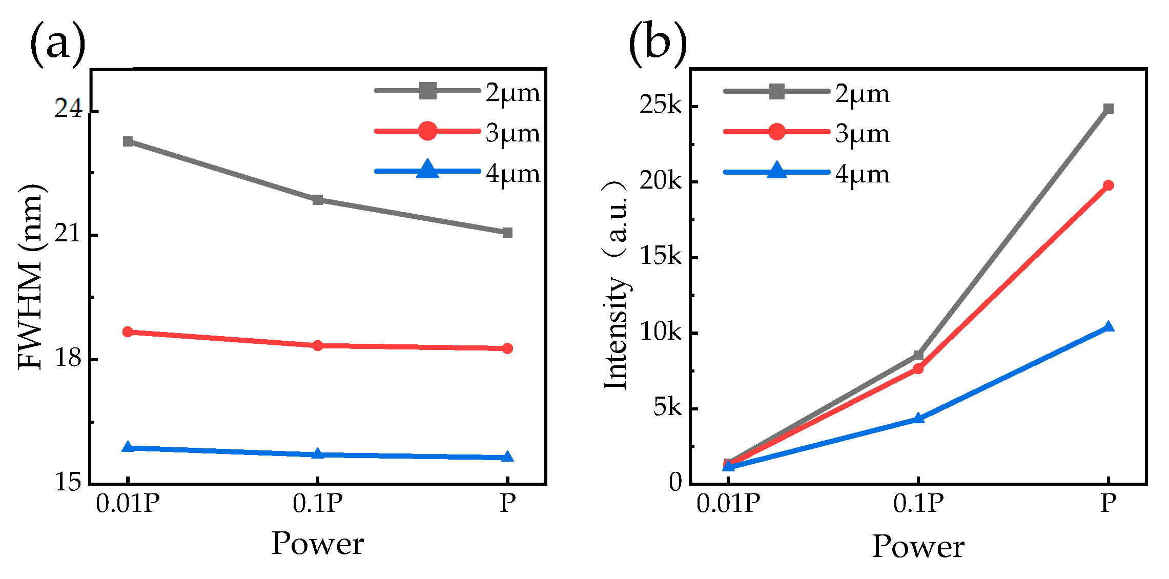
Figure 7.
CL mapping images of samples with different sizes. outer dashed lines indicate the microrod edges, inner dashed lines indicate the boundaries of the band-edge emission regions.
Figure 7.
CL mapping images of samples with different sizes. outer dashed lines indicate the microrod edges, inner dashed lines indicate the boundaries of the band-edge emission regions.
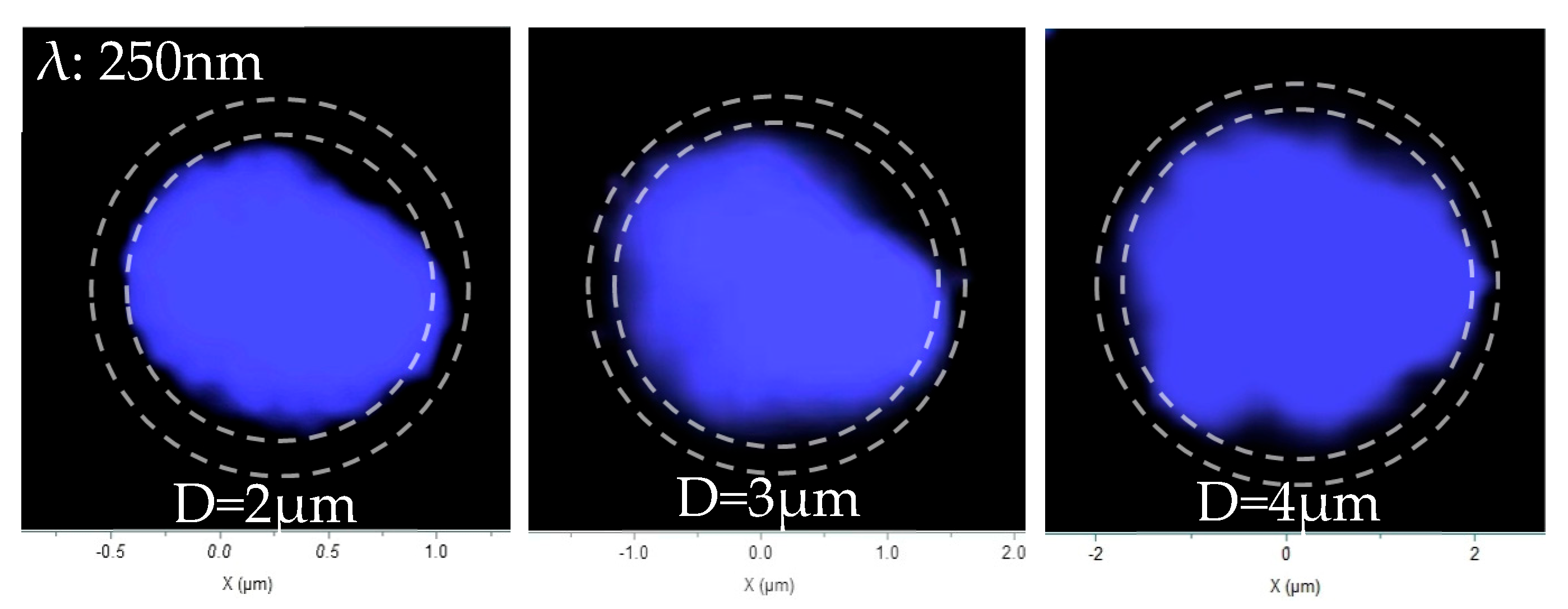
Figure 8.
Variation of the non–band-edge emission width for microrod of different sizes.
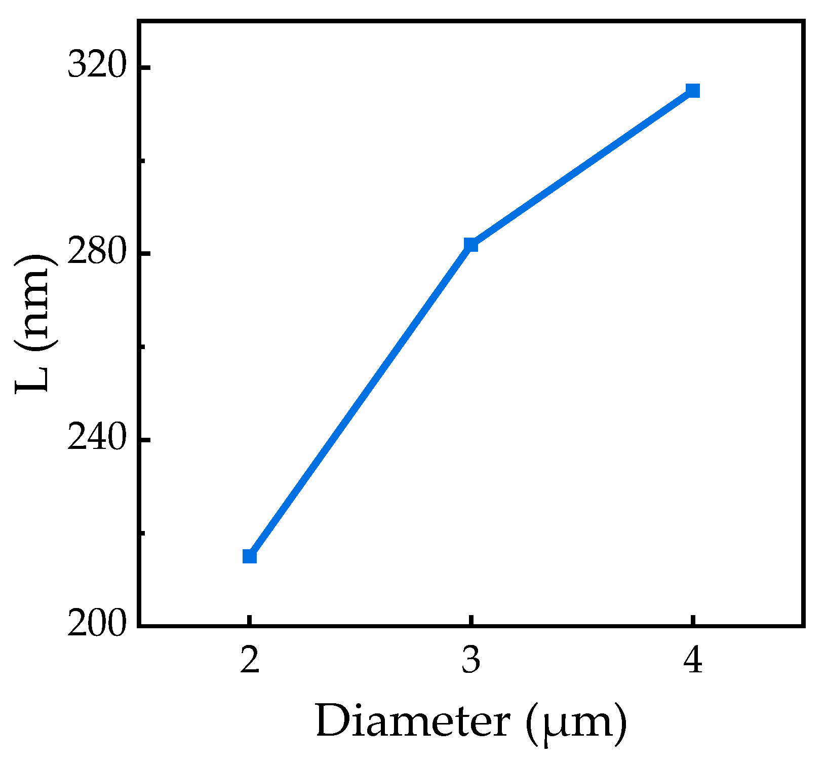
Figure 9.
CL mapping images of different luminescence peaks. dashed lines indicate the microrod edge contours.
Figure 9.
CL mapping images of different luminescence peaks. dashed lines indicate the microrod edge contours.
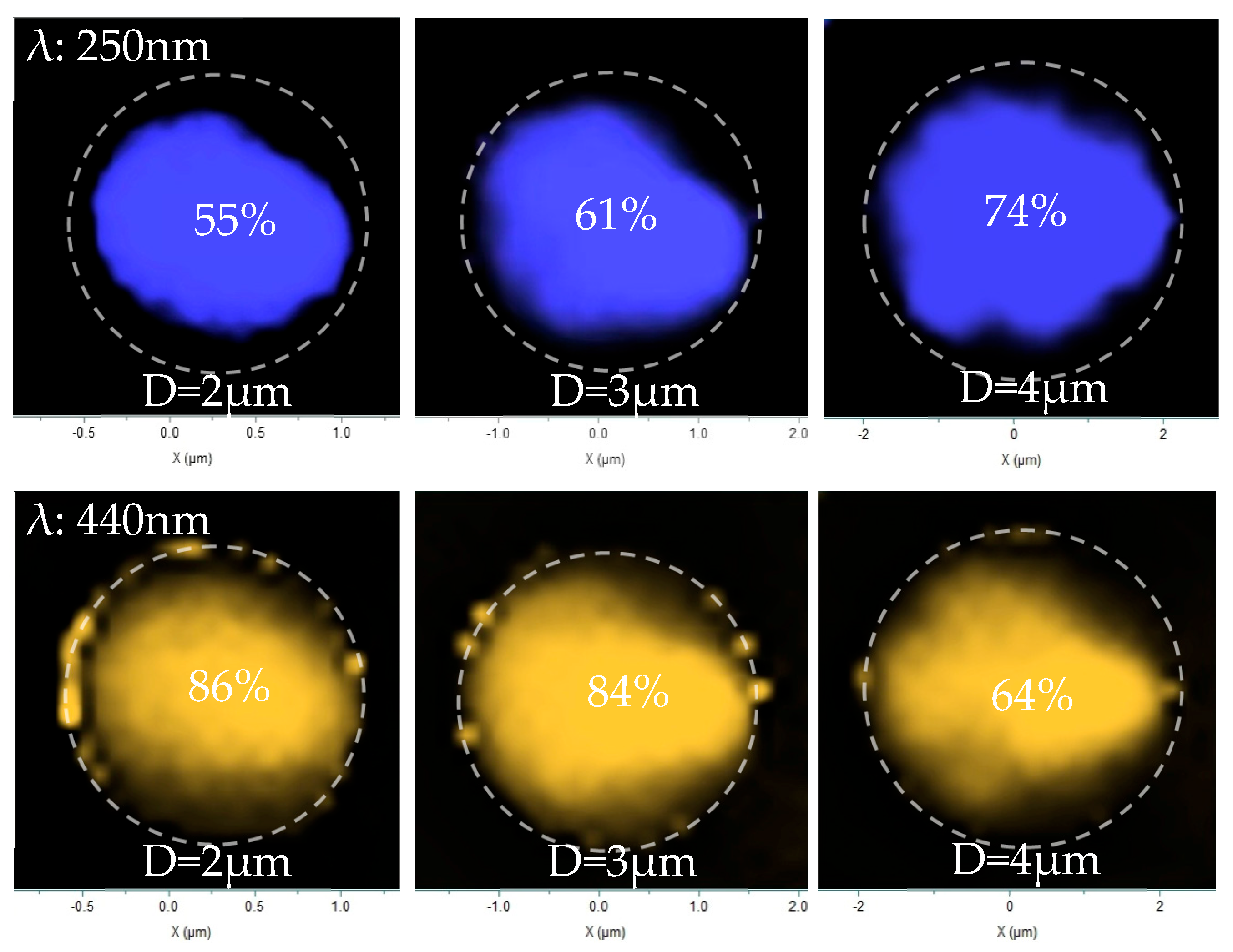
Figure 10.
Relative emission areas of different luminescence peaks.
Disclaimer/Publisher’s Note: The statements, opinions and data contained in all publications are solely those of the individual author(s) and contributor(s) and not of MDPI and/or the editor(s). MDPI and/or the editor(s) disclaim responsibility for any injury to people or property resulting from any ideas, methods, instructions or products referred to in the content. |
© 2026 by the authors. Licensee MDPI, Basel, Switzerland. This article is an open access article distributed under the terms and conditions of the Creative Commons Attribution (CC BY) license (http://creativecommons.org/licenses/by/4.0/).
Copyright: This open access article is published under a Creative Commons CC BY 4.0 license, which permit the free download, distribution, and reuse, provided that the author and preprint are cited in any reuse.


