Submitted:
11 February 2026
Posted:
12 February 2026
You are already at the latest version
Abstract
Micro-electro-mechanical systems (MEMS) sensors offer the benefits of compact size, lightweight design, and low cost, making them widely applicable in consumer electronics, vehicles, health, defense, and communications. With enhanced performance, MEMS sensors have also found applications in oil exploration and geophysical studies. For years, pressure and temperature sensing during hydraulic fracturing has been employed to enhance the down-hole conductivity of oil and gas extraction. Nevertheless, the pursuit of developing high-precision MEMS sensors for oil exploration continues to be an active area of research. This paper details the design, fabrication, packaging, and characterization of a silicon-on-insulator (SOI) MEMS piezoresistive pressure sensor integrated with a temperature sensor. It also describes the design of a chamber that simulates real conditions at the bottom of oil exploration wells. The sensors were successfully designed and fabricated based on physics-based simulations, deep reactive ion etching and anodic bonding techniques. The pressure sensors, along with the signal conditioning system, demonstrated a linear response, with a maximum linear error of 4.95% at 7 MPa and a reduced linear error of less than 3.5% at 24 MPa. Additionally, a quadratic approximation for the temperature sensors was achieved, showing a maximum resistance change of 8.5% at 140 ºC.
Keywords:
micro-electro-mechanical system
; pressure sensor
; temperature sensor
; finite element modelling
; silicon on insulator
; fabrication
; MEMS characterization
1. Introduction
Monitoring hydraulic fracturing is crucial for the development of unconventional oil and gas [1,2,3]. This process involves injecting high-pressure fluid into the target reservoir, which generates, expands, or connects cracks to the natural fractures. As a result, the porosity and permeability of underground reservoirs are enhanced, thereby boosting the productivity of unconventional oil and gas resources. During hydraulic fracturing, the most critical down-hole parameters are pressure and temperature. Consequently, the pressure sensors used in hydrocarbon wells must endure harsh conditions while maintaining accuracy, stability, and reliability over several weeks of measurement. Specifically, these pressure sensors must function at pressures up to 210 MPa and temperatures of approximately 210 °C [4].
Recent advancements in microfabrication and micro-electro-mechanical systems (MEMS) have been effectively leveraged by pressure sensors. MEMS technology has demonstrated particular efficacy in pressure sensing applications. Despite significant progress in the development of pressure sensors, the industry continues to seek novel MEMS solutions capable of meeting the demands of applications in harsh environments. In the subsequent discussion, the available technologies, including optical fiber, resonant, capacitive, piezoelectric, and piezoresistive types, are analyzed.
Various physical parameters, including acceleration, strain, humidity, and temperature, can be monitored using optical strain gauges or fiber optic sensors (FOS) [5,6,7]. Unlike traditional electrical sensors, FOS do not require an electrical supply, rendering them completely inert and immune to electromagnetic interference [5,7]. Among the various options, one of the most reliable FOS for downhole applications is based on the refractive index variation in a fiber Bragg grating (FBG) embedded in a fiber. The FBG expands or contracts in response to the pressure or force applied to the FOS, thereby altering the refractive index. However, detecting slowly varying strain with temperature changes poses a significant challenge because optical fibers are inherently very temperature-sensitive. Therefore, temperature compensation is necessary when using FOS for high-temperature and high-pressure measurements [8].
In resonant sensors, it is essential to stimulate the mechanical resonant frequency. This frequency is influenced by two primary parameters: the spring constant of the bending section and its effective mass, which vary based on these factors. This principle underlies the use of changes in the resonance frequency as a detection method [9,10]. To achieve the desired sensitivity and resolution, a high-quality factor is required [11]. MEMS resonators are characterized by low power consumption and the ability to operate at high frequencies with stability and precision. In addition, they can function across a wide range of pressures, making them ideal for industrial applications. However, despite these benefits, MEMS resonator pressure sensors are vulnerable to environmental influences such as temperature fluctuations and mechanical shocks, which can affect their performance and reliability. Furthermore, the fabrication process of MEMS resonators can be complex and costly, potentially limiting their widespread adoption in certain markets.
Capacitive sensors exhibit less temperature drift than piezoresistive sensors, because capacitance is generally not created through a diffusion method [12]. These sensors are typically constructed as standard parallel-plate capacitors. When the pressure-sensitive membrane, positioned on one or both sides of the sensor, undergoes a change, it alters the electrode separation or dielectric constant of the medium between the plates, thereby changing the capacitance. Capacitive pressure sensors operate effectively across a broad pressure range, from 250 Pa to 70 MPa [13]. Additionally, they offer high pressure sensitivity and low power consumption [14,15]. However, due to parasitic and stray capacitances, measuring the capacitance and linearizing the output signal presents challenges. Moreover, the manufacturing of capacitive sensors typically requires essential pretreatments, sophisticated equipment, and high process temperatures [16].
Mechanical stress is transformed into analog voltage via piezoelectric sensors [17,18,19]. When pressure is applied, the piezoelectric crystal structure is deformed, thereby altering the internal dipole moment of the piezoelectric material. Consequently, the electrical surface potential changes in response to the applied force. This characteristic allows piezoelectric sensors to require minimal energy, as they are self-powered. Due to their excellent piezoelectric properties, piezoelectric ceramic materials, such as PZT, , ZnO, and AlN [20] are frequently used as piezoelectric transducers. These sensors can measure a wide range of pressures, typically from 0.7 kPa to 70 MPa, and are renowned for their high sensitivity, accuracy, and robustness [13]. However, the design of the electronic interface is more complex than that of other sensor types. A charge amplifier is necessary to convert the very high-impedance charge output into a voltage signal, and must be positioned close to the sensing element [13].
The earliest and most widely used type of pressure sensors are piezoresistive ones. Typically, resistive components are deposited, implanted, or diffused onto a membrane that is sensitive to stress [12,21,22,23,24]. Hence, the variation in piezoresistors caused by the induced stress in the membrane is converted into a voltage output owing to the piezoresistive effect. Materials such as single crystal silicon, polysilicon, and are frequently used to construct pressure-sensitive diaphragms for piezoresistive sensors. These sensors, particularly those based on silicon, have excellent sensitivity, linearity, and straightforward signal processing [25]. However, the main drawbacks of piezoresistive sensors are their relatively high power consumption and temperature dependence of the sensor output, which must be compensated electronically.
Conversely, numerous types of temperature sensors have been developed using MEMS technology, including capacitive, resonant, piezoresistive, and resistor-based types. Capacitive temperature sensors typically consist of two separate capacitor plates or comb drive structures. The distance between these plates, or the overlapping area of the comb structures, changes with temperature [26]. Resonant temperature sensors depend on frequency variations in the resonator caused by thermal strain. This strain primarily arises from the different thermal expansion coefficients of the substrate and device layers of the fabricated structures [27]. Piezoresistive temperature sensors function based on the principle of stress-induced resistance changes in the embedded piezoresistor. Thermal stress is generated by mismatches in the thermal expansion coefficients of materials within the structure [28]. Resistor-based temperature sensors utilize a temperature-sensitive resistor or thermistor to measure temperature, exploiting the principle that the electrical resistance of certain materials changes predictably with temperature [29].
The aim of this work was to design a miniaturized pressure sensor integrated with a temperature sensor to monitor the conditions at the bottom of oil exploration wells in the Chicontepec region of Veracruz, Mexico, during hydraulic fracturing operations. The device must function reliably at temperatures between 90 and 115 °C and withstand pressures of up to 70 MPa. Furthermore, strict packaging constraints require that the total diameter of the sensor die assembly does not exceed 2 mm per side. Considering these design requirements, along with the analysis presented in this section and the capabilities of the available fabrication equipment, piezoresistive pressure and resistive temperature sensing approaches were selected. The fabrication was based on silicon-on-insulator (SOI) technology, deep reactive ion etching (DRIE), and anodic bonding processes.
2. Materials and Methods
In this section, the design and fabrication processes of piezoresistive pressure sensors and resistive temperature sensors are explained. Initially, a general structure of MEMS sensors is introduced, followed by an in-depth exploration of the pressure sensor design, including finite element modelling. Subsequently, the design and finite element modelling of the temperature sensor are discussed. Finally, the fabrication stages are described in detail.
2.1. MEMS Sensors Structure
The MEMS structure was fabricated using a standard microfabrication process based on SOI technology. This approach allows for a more flexible selection of the resistivity values of the active layer, which helps to better define the values of the piezoresistive elements and facilitates the formation of ohmic contacts on these elements, thereby eliminating the need for an ion implantation process [30]. The active layer was isolated from the handle wafer using a 2m-thick buried oxide (BOX) layer. This active layer was machined to define the piezoresistive pressure sensors and resistive temperature sensors. A membrane was constructed on the handle wafer by etching the bottom side of the SOI wafers, with the membrane connected to the active layer through the BOX layer.
2.2. Design and Simulation of Pressure Sensor
The geometry of the membrane is crucial for pressure sensors. Designs featuring rectangular membranes exhibit maximum stress at the center of each side of the perimeter. In this study, a circular membrane was selected because of its uniform stress and strain distributions along the perimeter, as illustrated in Figure 1. The strain in a circular membrane is less than the maximum stress observed in rectangular membranes of the same area and thickness. A membrane-isolated chamber was created by partially machining the handle side of the SOI wafer using the DRIE BOSCH process, followed by a wafer bonding process with a Borofloat 7740 wafer to form a sealed enclosure.
To effectively utilize piezoresistive conversion, the orientation of the piezoresistors in the design of pressure sensors must be precisely determined. It is widely recognized that p-type silicon demonstrates a significant piezoresistive effect when aligned along the [110] direction [31,32]. When stress is applied to p-type silicon in this orientation, the valence bands, including the light and heavy hole bands, split and warp, enhancing their mobility and resulting in substantial changes in resistivity. Consequently, SOI wafers with a (100) plane, a 5 m thick p-type active layer with a resistivity of 0.015 -cm, and a 450 m thick handle wafer were chosen for the pressure sensor implementation. Anisotropic chemical etching with potassium hydroxide (KOH) extends from the active layer to the BOX layer, defining piezoresistive structures. The non-vertical profile of the KOH-etched active layer was formed by the intersection of the (111) and (100) planes. Additionally, this non-vertical profile facilitated the proper continuity of the metal lines from the top (100) plane through the resulting (111) plane, post-KOH, and down to the BOX layer parallel to the (100) plane.
Finite element simulations were performed using COMSOL Multiphysics version 4.0 software [33] to investigate how different parameters of the silicon structure model affect the surface stress experienced by the piezoresistive elements. The mechanical properties of the membranes were determined numerically by applying pressure to the active layer side of the sensor, utilizing a Young’s modulus of and Poisson’s ratio of for silicon [34]. To determine the appropriate size and thickness of the circular membrane, multiple finite element models were analyzed across a range of membrane thicknesses and diameters to ensure that the yield strength of 7.7 GPa for silicon did not exceed [35].
First, serpentine shaped piezoresistive sensing elements were designed following the resistive rosettes model proposed in [36,37] as shown in Figure 1(a). Subsequently, four piezoresistors were defined along the radial and circumferential membrane axes, along the [110] direction, positioned at the membrane edge region as shown in Figure 1(b). This configuration ensures that the resistance of the two longitudinal piezoresistors increases due to the positive coefficient, and that of the two transverse piezoresistors decreases owing to the negative coefficient when pressure is applied to the membrane [36,37].
2.3. Design and Simulation of Temperature Sensor
Temperature sensors were strategically positioned in the unstressed regions of the membrane to ensure that they primarily responded to the temperature changes. However, owing to the constraints of die dimension specifications, they cannot be placed too far from the membrane edge. Figure 1(b) illustrates the proposed layout designed to minimize piezoresistive contributions when these thermal resistors are integrated near the membrane of the pressure sensor. The design was evaluated through a finite element simulation of two different temperature resistor layouts, as shown in Figure 2. One layout features a simple serpentine with elements aligned along the [110] crystal direction (see Figure 2(b)), whereas the other employs the proposed mixed serpentine design (see Figure 2(a)). The proposed design incorporates a combination of elements arranged both parallel and perpendicular to the [110] crystal direction, forming a mixed serpentine shape. In this configuration, individual elements experience both positive and negative resistance changes due to strain deformation outside the membrane perimeter, as depicted in Figure 2(a). This design effectively cancels out the piezoresistive contributions across different silicon elements [38]. The advantage of this temperature sensor layout is its ability to optimize the total die area of the sensor.
2.4. Fabrication of Sensors
This section summarizes the fabrication steps for the pressure and temperature sensors. As shown in Figure 3, the fabrication steps are as follows:
- (a)
- Start with a SOI wafer consisting of a 5 m device layer (100) plane with a resistivity of 0.015 -cm, a BOX layer of 2 m and a 450 m handle wafer with a resistivity of 10 -cm.
- (b)
- The SOI wafer was subjected to a dry oxidation process for 30 minutes at 1000 °C for 110 nm growth on both sides of the wafer. Then, a 100 nm chrome layer was deposited on the bottom of the wafer using sputter deposition at a rate of 0.75 Å per second for the first 25 nm, and then the rate was increased to 1.0 Å per second for a total deposition of 60 nm.
- (c)
- Structures were defined on the device layer using the Shipley’s S1813 photoresist. These include piezoresistive pressure and resistive temperature sensors, as well as supportive structures that facilitate subsequent wafer bonding procedures, as outlined in step (l). A buffered oxide etch (BOE) was used to etch the top oxide, ensuring that the defined structures remained protected by the photoresist and oxide.
- (d)
- The top device layer was etched with KOH at 82 °C until it reached the BOX layer. A slightly modified design mask, combining both triangular and rectangular structures, was used, which differed from that employed by [37].
- (e)
- A thick layer of photoresist was deposited and defined with narrower features (undersized) from the device feature mask design, to leave only narrow openings on top of the device structures. This process covered the top edges of the device structures and their exposed sidewalls, resulting from the KOH process.
- (f)
- The previous photoresist protective layer enabled to proceed with a BOE of . The photoresist thoroughly protects the bottom BOX layer, particularly at its oxide interface with the KOH machined sidewalls of the device structures.
- (g)
- After stripping the photoresist and etching the bottom chrome, the SOI wafer undergoes a piranha cleaning process. This was followed by a second dry oxidation process to grow 80 nm of . Subsequently, 100 nm of chrome was deposited on the bottom of the wafer using sputter deposition. The deposition rate was initially set at 0.75 Å per second for the first 25 nm, then increased to 1.0 Å per second for the remaining 75 nm.
- (h)
- In the next step, photoresist is used to define a sacrificial mask on the device side layer, featuring narrow openings to facilitate the BOE in the BOX layer. The layout definition of these openings is crucial for the subsequent anodic bonding process [36]. Due to the isotropic nature of the BOE, an undercut profile is formed in the BOX layer from the narrow openings in the photoresist. A 60 nm aluminum sputter deposition was then applied to the device side, allowing metal deposition on certain sections of the handle wafer through the openings in the BOX layer.
- (i)
- After cleaning the photoresist, the top metal is lifted-off, leaving only the aluminum on the BOX layer’s openings. Then, a second lift-off process was performed on the device layer to define a sacrificial layer by sputter deposition of 200 nm of chrome. This metal forms a connection between the top section of the device structures and the handle wafer through BOX openings. It is important to note that the metal maintains a continuous connection from the top section of the device structures through its micromachined sidewalls to the top face of the BOX and through the smoothly isotropic etched shape of the BOX layer to the handle wafer.
- (j)
- The SOI wafer is coated with photoresist on both sides. The photoresist on the handle wafer side is patterned, and the chrome and oxide layers on the handle wafer are etched.
- (k)
- The patterned handle wafer defines the cavity of the pressure sensor by partially etching silicon using a DRIE process. Each DRIE cycle consisted of a passivation step followed by an etching step, with specific process chamber conditions (gas flow and power settings) as follows: the passivation step used 76 sccm of , 8 W of forward RF power, and 805 W of ICP power for 5 s; the etching step employed 76 sccm of , 27 W of forward RF power, and 765 W of ICP power for 5 s. Each cycle etched an average of 0.3 m of silicon. This process defines the pressure sensor membrane, resulting in a final thickness of 190 m. Dry etching with is used to clean the remaining photoresist on the handle wafer, followed by wet etching of the chrome and oxide layers of the handle wafer.
- (l)
- The bottom layer of chrome on the handle wafer was wet etched, followed by BOE of the handle oxide layer. The photoresist from the device side was stripped, and the wafer was cleaned using the piranha process before anodic bonding of the SOI and Borofloat wafers. The metallized top layer acted as an electrode for the surrounding contacts in the pressure cavity, ensuring the proper current flow required for the anodic bonding process at the interface between the handle and glass wafers. The parameters utilized in the SB6/8 wafer bonder for the anodic bonding of the SOI and Borofloat wafers were as follows: a membrane pressure of 150 kPa, a vacuum of mBar, a temperature of 280 °C, a voltage of 1000 V, and a maximum current of 12 mA. During the bonding process, the current remained constant at 12 mA for 100 s before decreasing exponentially to 240 A after 7 min and 23 s.
- (m)
- After bonding the wafers, the sacrificial top chrome contacts were etched to prepare for the formation of ohmic contacts on the upper surface of the device structures, specifically the piezoresistive sensors.
- (n)
- A lift-off photoresist was employed to define openings in specified regions for ohmic contacts on the device layer of the pressure and temperature sensors. Subsequently, 75 nm of Al/Si (95% and 5%, respectively) was deposited at 164 °C via sputtering. The utilization of an Al/Si alloy facilitates its diffusion into silicon, thereby forming ohmic contacts.
- (o)
- After cleaning the lift-off photoresist, a new lift-off photoresist was applied to define wider openings for the ohmic contact regions on the top of the sensors. Subsequently, a second sputter deposition of 75 nm of Al/Si (95% and 5%, respectively) at 174 °C was performed.
- (p)
- A 50 nm chromium sputter deposition was used to temporarily protect the top Al/Si interface from oxidation. The lift-off photoresist was cleaned, and the bonded wafers were cleaned with piranha solution. Then, to establish ohmic contacts, thermal treatment in an inert gas environment at 450 °C for 30 min was used.
- (q)
- After the ohmic contact was formed, the oxidized top chrome was stripped off. Using photoresist for lift-off, a new 75 nm layer of sputtered chrome was deposited, followed by 250 nm of gold evaporative deposition on the device layer, culminating in a final lift-off process. Chrome and gold were smoothly deposited from the top of the device structures and connected through the machined sidewalls to define the metallized interconnections of a full Wheatstone bridge circuit. This metallization procedure was also used to connect the contact pads for wire bonding immediately after the chips were diced from the wafer. First the dicing process partially cuts the Borofloat wafer from the bottom.
3. Results
A three-dimensional model of the MEMS structure was developed using COMSOL simulations. Figure 4 shows the results of the membrane structure simulation. Figure 4(a) shows the Von Misses stress as a function of the applied pressure in the range of 7 MPa to 70 MPa for membrane thicknesses of 100, 150, 200, 250, and 300 m, and a diameter of 1550 m. Based on these results, the final design was selected with a membrane thickness of 190 m, corresponding to a Von Mises stress value of 20% of the fracture strength of silicon. For the chosen membrane dimensions, Figure 4b and Figure 4c show the distributions of Von Mises stress at both the upper and lower surfaces of the membrane under a pressure of 70 MPa.
Figure 5 shows the simulation results for the temperature resistor structures depicted in Figure 2(a) and Figure 2(b). In Figure 5(a), the Von Mises stress distribution under an applied pressure of 70 MPa at a constant temperature is shown, with both resistor structures positioned 20 m from the membrane edge. Figure 5(b) compares the relative resistance change for the two resistor configurations when subjected to an applied pressure of 70 MPa at the center of the membrane.
The complete design of the MEMS sensor, including the supportive structures, BOX openings, and metal layers, is shown in Figure 6. Figure 6(a) shows the layout of the design with four pressure piezoresistors and four temperature resistors. The cross-section of the supportive structure is shown in Figure 6(b). As shown, the metal layer was deposited along the inclined sections of the KOH etched edges of the device structures, connecting the device layer to the handle wafer. Figure 6(c) shows the cross section of both the pressure sensor and bonding support structure, located at the top left and top right, respectively.
The MEMS sensor, which features four pressure sensors arranged in a full Wheatstone bridge signal conditioning configuration and four temperature sensors, is illustrated in Figure 7. Figure 7(a) shows a top view of the MEMS sensors along with their supporting structures. Figure 7(b) depicts a perfilometer image, obtained with a Dektak Bruker perfilometer, of the supporting structure of two adjacent dies. The MEMS sensor chips were glued with silver paint from the bottom section and wire-bonded into a 48-pin dual in-line package, with each package containing four dies, as shown in Figure 7(c).
An experimental setup was developed to characterize the pressure and temperature sensors and to validate the performance of the proposed design. The setup for measuring pressure at various temperatures is shown in Figure 8. A chamber for high-pressure conditions was developed to test the piezoresistive sensors. The design included a low-cost, three-stage pressure system comprising: 1) a manual deadweight tester DWT1305D-100; 2) a piston cylinder symplex RC-series connected to an auxiliary chamber designed to separate testing fluids (see Figure 8); and 3) a custom-designed stainless steel chamber with eight Conax high-pressure feedthroughs HPPL14, each equipped with six 24AWG electrical cables (see Figure 8). The three-stage system enabled the separation of the specialized hydraulic fluid utilized by the deadweight tester from the oil under test with MEMS sensors. It also facilitated the testing of high-pressure and temperature sensors using up to 48 individual electrical lines. All designed chambers adhered to the autoclave high-pressure standard specification for all connections. The pressure of the system was continuously monitored via RS-232 communication using an Additel 681-series high-precision gauge sensor, as illustrated in Figure 8. Furthermore, the two interconnected chambers, processing electronic circuit, and feedthroughs are depicted.
Figure 9 illustrates the stainless-steel chamber design. The auxiliary chamber, depicted in Figure 9(a) as a fluid separator, and the testing chamber, shown in Figure 9(b)-(e), were both designed to endure 70 MPa of pressure, utilizing a finite element simulation with a safety factor of 4. The upper chamber in Figure 9(a) corresponds to the lower chamber shown in Figure 8. Below this chamber, the Simplex piston was attached (not shown in Figure 8). The deadweight tester provides pressure to the piston, which pressurizes the internal testing oil in the auxiliary chamber. This pressurized oil was then linked to the testing chamber, positioned on top of the auxiliary chamber as depicted in Figure 8. The testing chamber was designed with a height of , a diameter of , and an internal diameter of . It also featured a depth of to facilitate sensor handling and testing. During the finite element simulation of the stainless-steel chamber, as shown in Figure 9(c), the maximum Von Mises stress recorded was less than 20% of the yield tensile strength of 2.1 GPa for the AISI 302 austenitic stainless steel [30].
As illustrated in Figure 6(a), four piezoresistors were aligned along the radial and circumferential axes of the membrane in the [110] direction. Positioned at the edge of the membrane, they were connected in a full Wheatstone bridge configuration to measure the piezoresistive response of the pressure sensor. With the layout depicted in Figure 6(a) and a device layer resistivity of 0.015 -cm, each serpentine-shaped piezoresistor exhibited a static resistance (under zero-pressure conditions) of . Figure 6(a) also shows the directions of the longitudinal stress and transverse stress . Piezoresistors and are subjected to stresses that are oriented at 90 °C relative to those affecting and . Consequently, the longitudinal stress component for and corresponds to the transverse stress component for and , and vice versa. The relative change in the resistance for each piezoresistor can be expressed as
where is the Poisson’s ratio of silicon, and and are the longitudinal and transverse piezoresistive coefficients, respectively.
As shown in Figure 8, an electronic circuit was employed to ensure accurate calibration of the sensor signals. Figure 10 shows the schematic circuit designed to measure the piezoresistive response of each full Wheatstone bridge. and represent the relative resistance changes of the piezoresistive elements, as given by Equation (1). Under conditions of zero pressure, the resistances are equal, such that . The input-output relationship for the Wheatstone bridge is expressed by
The circuit design incorporates INA2126 operational amplifiers, a voltage supply of , and stages for pre-amplification, offset calibration, and amplification. The total gain achieved was 76. Given that in practice and , the Wheatstone bridge exhibits minor nonlinearity, as depicted in Figure 11 for the measured output voltage of four sensors tested up to 55 MP.
From Equation(2), the sensor sensitivity is given by
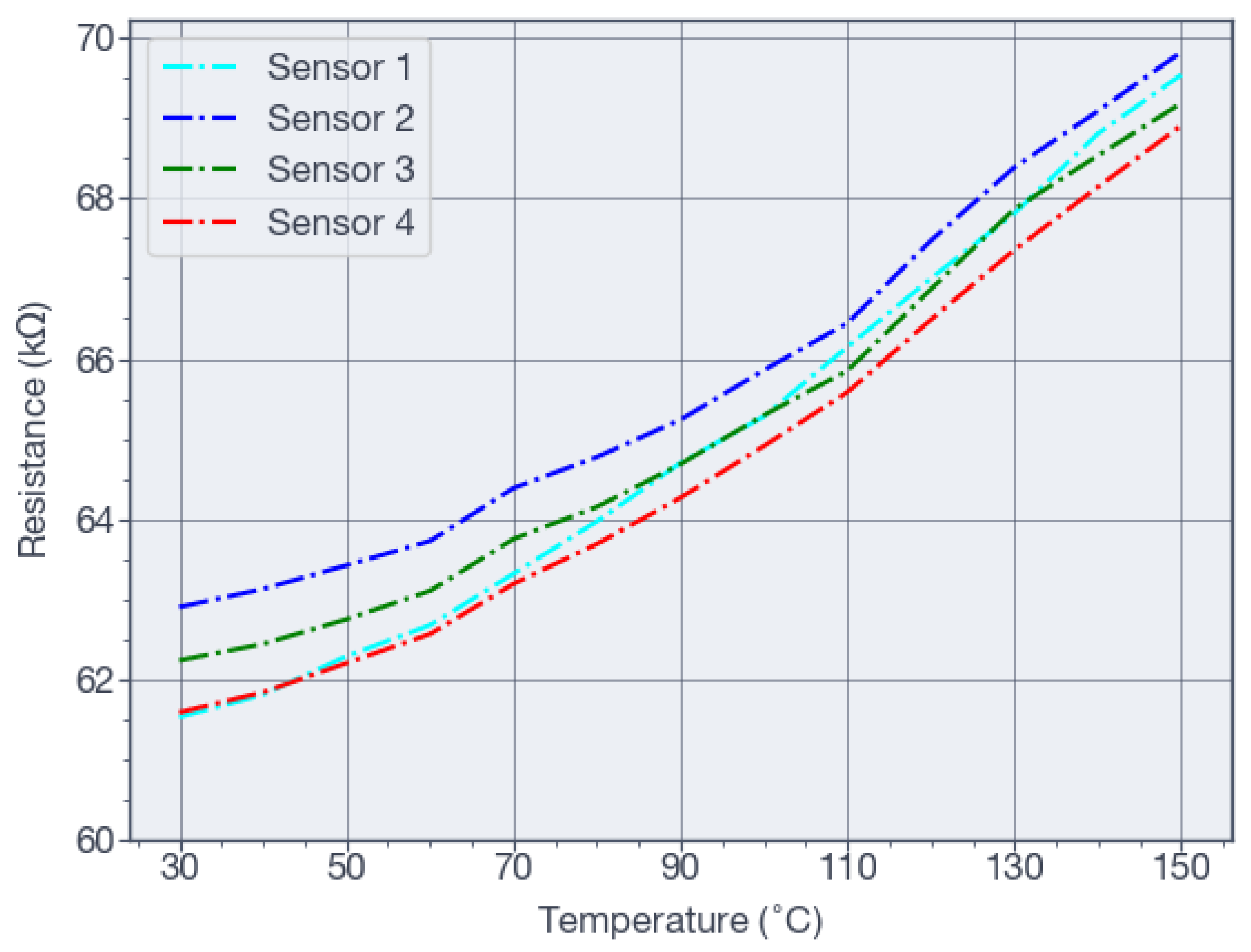
The implementation of the temperature sensors is intended to directly measure the operational temperatures at the bottom of the well. This approach also compensates for minor variations in the piezoresistive elements caused by temperature fluctuations. The design incorporates four resistive temperature sensors on each die sensor, as depicted in Figure 6(a) and Figure 7(a). Two resistors were connected in series, and these two sets were arranged in parallel, with measurements taken from two opposite corners. All temperature tests were conducted using a Barnstead Thermolyne 48000 electric furnace, within a temperature range of 30 °C to 150 °C, in increments of 10 °C. Figure 12 presents the resistance values for the four sensors, as measured using an Agilent 34401 meter.
The resistance exhibited an average increase of 8.5% over the temperature range of 32 °C to 140 °C. The quadratic approximation of the change in resistance as a function of temperature is expressed by
where represents the resistance in k, and T denotes the temperature in Celsius.
4. Discussion
The final design of the MEMS pressure sensor was determined based on the results of the finite element simulations, as depicted in Figure 4 and Figure 5. The MEMS structure comprises a membrane with a diameter of 1550 m and a thickness of 190 m. According to the simulation results presented in Figure 4(b) and Figure 4(c), at a maximum applied pressure of 70 MPa, the maximum displacement at the membrane center was 9.5 m, and the maximum Von Mises stress at the inner edge was 1418.81 MPa (see Figure 4(a)), which represents approximately 20% of the yield strength of silicon. Maximum strain deformation was observed along the membrane edge, as illustrated in Figure 4(b) and Figure 4(c), where the four piezoresistors were positioned. The results shown in Figure 5 were used to determine the placement of the temperature resistors, as depicted in Figure 2(a). The findings in Figure 5(b) for an applied pressure of 70 MPa at a constant temperature indicate a reduction in the percentage of piezoresistance change (less than 1.6%) for the temperature resistor of Figure 2(a), compared to a 9.2% piezoresistive change for the design shown in Figure 2(b) when the temperature resistors are located 20 m from the edge of the membrane. The proposed design is applicable to smaller die dimensions by positioning temperature sensors near the stress regions on the membrane edge because of its advantageous self-cancelling piezoresistive effect.
Anodic bonding of the handle side of the SOI wafer to the Borofloat wafer is a critical step in the fabrication process, specifically step l), as shown in Figure 3. This bonding process requires a voltage with a minimum activation energy of 0.97 eV to initiate the bonding effect [39]. The presence of a thick dielectric layer of 2 m on the SOI wafers impedes current flow through the wafers, complicating the achievement of the requisite activation energy for bonding the handle side of the SOI wafer to the Borofloat wafer. Although a BOX layer thickness of 380 nm has been successfully employed to bond Borofloat and SOI wafers [40], an alternative method is required for thicker BOX layers. Most anodic bonding systems utilize a limited current ranging from 5 mA to 15 mA for at least one minute to achieve an activation energy on the anodic bond surface at 1000 V for silicon and Borofloat wafers of . Consequently, in step i) of the fabrication process (see Figure 3) a thin layer of chrome was deposited in the openings. This metal layer is electrically connected to the supporting structures, facilitating current flow during anodic bonding. The MEMS structure uses support structures at the edges of sensor devices to withstand mechanical pressure. Without these supports, the sensing structures might break because of the mechanical force required for the anodic bonding process. Figure 7(b) illustrates four supportive structures at the center with BOX openings on their sides. They are flanked by two temperature sensors on the left and right, corresponding to two distinct sensor devices. In addition, larger structures featuring internal BOX openings are observed at the top and bottom. Figure 7(a) also displays the final dicing regions of the device structures, which cut the supportive structures by half.
The characterization phase was limited by the Viton O-ring employed in the testing chamber of Figure 8, which was capable of withstanding a maximum pressure of 55 MPa. Consequently, the pressure limit during the tests was 79% of the initial target. The results presented in Figure 11 demonstrate a maximum linear error of 4.95% at 7 MPa, which decreased to less than 3.5% upon reaching a pressure of 24 MPa. These findings were obtained under the assumption that the Additel pressure sensor (depicted in Figure 8) provided an accurate reading and that the temperature remained constant at 32 °C. The measurement results of Figure 11 showed that the full-scale output of the pressure sensor was 16.6 V and the sensitivity was 301.81 mV/MPa. During pressure testing, a hysteresis effect was observed in the sensors, with an error of approximately 0.2 MPa following the first high-pressure testing cycle and approximately 0.13 MPa after the second cycle.
5. Conclusions
A high-sensitivity MEMS piezoresistive pressure sensor, integrated with a temperature sensor, was successfully designed, fabricated, and characterized for downhole applications. These sensors are intended to facilitate the monitoring of the hydraulic fracturing process and are thus engineered to withstand conditions of 70 MPa and 90 °C. The piezoresistive elements were effectively designed by appropriately selecting an active layer resistivity of 0.015 -cm, thereby obviating the need for an ion implantation process. Temperature resistors were successfully positioned near the edge of the membrane of the pressure sensor owing to the self-cancellation of the piezoresistive effect by a combination of longitudinal and transverse serpentine-like structures. The proposed fabrication process utilizes SOI wafers and, incorporates DRIE and anodic bonding techniques. The auxiliary structures on the device layer facilitated the anodic bonding of the SOI and Borofloat wafers. A cost-effective high-pressure testing system was developed to enable the testing of sensors at up to 55 MPa and 150 °C. The fabricated pressure sensors exhibited a linear response with a sensitivity of 301.81 mV/MPa. Furthermore, a quadratic response of the temperature sensors was achieved, with a maximum percentage change in the resistance of 8.5% at a temperature of 140 °C. We will further investigate the hysteresis effect observed in both the pressure and temperature sensors.
Author Contributions
Conceptualization, J.M.; Data curation, J.M. and A.S.; Investigation, A.J.; Methodology, J.M. and A.S.; writing—original draft preparation, A.J.; writing—review and editing, J.M. and A.S.; All authors have read and agreed to the published version of the manuscript.
Funding
This research was funded by “SECIHTI-MX grant number MADTEC-2025-M-721”, Programa Presupuestario F003 “Programas Nacionales Estratégicos de Ciencia, Tecnología y Vinculación con los Sectores Social, Público y Privado.”
Institutional Review Board Statement
Not applicable.
Informed Consent Statement
Not applicable.
Data Availability Statement
The raw data supporting the conclusions of this article will be made available by the authors on request.
Conflicts of Interest
The authors declare no conflicts of interest.
Abbreviations
The following abbreviations are used in this manuscript:
| MEMS | Micro-electro-mechanical systems |
| SOI | Silicon-on-insulator |
| FOS | Fiber optic sensors |
| FBG | Fiber Bragg grating |
| DRIE | Deep reactive ion etching |
| BOX | Buried oxide |
| KOH | Potassium hydroxide |
| BOE | Buffered oxide etch |
References
- Sun, H.; He, N.; Application and Research of Microseismic Monitoring System and Hydraulic Fracturing Technology in Coal Mines. Water 2024, 16, 1062. [CrossRef]
- Hu, J.; Fu, M.; Yu, Y.; Li, M. New Method for Monitoring and Early Warning of Fracturing Construction. Processes; 2024, 12, 765. [CrossRef]
- Li, R.; Zhai, H.; Jiang C.; Zhu, W.; Li, X.; Wang, Z.; Wang, Y. A review of laboratory hydraulic fracturing experiments on shales. Geoenergy Sci. Eng.; 2025, 254, 214028. [CrossRef]
- Patel, M.S.; Sinha, B.K. A Dual-Mode Thickness-Shear Quartz Pressure Sensor for High Pressure Applications. IEEE Sens. J.; 2018, 18, 4893-4901. [CrossRef]
- Pendão, C.; Silva, I. Optical Fiber Sensors and Sensing Networks: Overview of the Main Principles and Applications. Sensors; 2022, 22, 7554. [CrossRef]
- Johny, J.; Amos, S.; Prabhu, R. Optical Fibre-Based Sensors for Oil and Gas Applications. Sensors; 2021, 21, 6047. [CrossRef]
- Tosi, D.; Molardi, C.; Sypabekova, M.; Blanc, W. Enhanced Backscattering Optical Fiber Distributed Sensors: Tutorial and Review. IEEE Sens. J.; 2021, 21, 12667–12678. [CrossRef]
- Zhao, N.; Zhang, Z.; Lin, Q.; Yao, K.; Zhu, L.; Chen, Y.; Zhao, L.; Tian, B.; Yang, P.; Jiang, Z. Research on the High Temperature and High Pressure Gold-Plated Fiber Grating Dual-Parameter Sensing Measurement System. Micromachines; 2022, 13, 195. [CrossRef]
- Verma, G.; Mondal, K.; Gupta, A. Si-based MEMS resonant sensor: A review from microfabrication perspective. Microelectron. J.; 2021, 118, 105210. [CrossRef]
- Morten, B.; De Cicco, G.; Prudenziati, M. Resonant pressure sensor based on piezoelectric properties of ferroelectric thick films. Sens. Actuators A: Phys.; 1992, 31, 153-158. [CrossRef]
- Miller, J.M.L.; Ansari, A.; Heinz, D.B.; Chen, Y.; Flader, I.B.; Shin, D.D.; Villanueva, L.G.; Kenny, T.W. Effective quality factor tuning mechanisms in micromechanical resonators. Appl. Phys. Rev.; 2018, 5, 041307. [CrossRef]
- Yao, Z.; Liang, T.; Jia, P.; Hong, Y.; Qi, L.; Lei, C.; Zhang, B.; Xiong, J. A High-Temperature Piezoresistive Pressure Sensor with an Integrated Signal-Conditioning Circuit. Sensors; 2016, 16, 913. [CrossRef]
- Avnet Abacus Pressure Sensors: The Design Engineer’s Guide Available online: https://www.avnet.com/wps/portal/abacus/ solutions/technologies/sensors/pressure-sensors (accessed on 12 June 2025).
- Arefin, M.S.; Redouté, J.M.; Yuce, M.R. A Low-Power and Wide-Range MEMS Capacitive Sensors Interface IC Using Pulse-Width Modulation for Biomedical Applications. IEEE Sens. J.; 2016, 16, 6745-6754. [CrossRef]
- Zhang, C.; Gallichan, R.; Budgett, D.M.; McCormick, D. A Capacitive Pressure Sensor Interface IC with Wireless Power and Data Transfer. Micromachines; 2020, 11, 897. [CrossRef]
- Abdul, B. Development of a Novel Silicon Membrane MEMS Capacitive Pressure Sensor for Biological Applications. Eng. Proc.; 2023, 48, 54. [CrossRef]
- Seo, Y.; Kim, D.; Hall, N.A. Piezoelectric Pressure Sensors for Hypersonic Flow Measurements. JJ. Microelectromech. Syst.; 2019, 28, 271-278. [CrossRef]
- Kordrostami, Z.; Hassanli, K.; Akbarian, A. MEMS piezoresistive pressure sensor with patterned thinning of diaphragm. Microelectron. Int.; 2020, 37, 147-153. [CrossRef]
- Song, P.; Ma, Z.; Ma, J.; Yang, L.; Wei, J.; Zhao, Y.; Zhang, M.; Yang, F.; Wang, X. Recent Progress of Miniature MEMS Pressure Sensors. Micromachines; 2020, 11, 56. [CrossRef]
- Wei, H.; Wang, H.; Xia, Y.; Cui, D.; Shi, Y.; Dong, M.; Liu, C.; Ding, T.; Zhang, J.X.; Ma, Y.; Wang, N.; Wang, Z.; Sun, Y.; Wei, R.; Guo, Z. An overview of lead-free piezoelectric materials and devices. J. Mater. Chem. C; 2018, 6, 12446–12467. [CrossRef]
- Mireles, J.Jr.; Estrada, H.; Ambrosio, R.C. Sensors for hydraulic-induced fracturing characterization. In Proceedings of SPIE 8031, Micro- and Nanotechnology Sensors, Systems, and Applications III, Orlando, Florida, United States, 13 May 2011. [CrossRef]
- Niu, Z.; Zhao, Y.; Tian, B. Design optimization of high pressure and high temperature piezoresistive pressure sensor for high sensitivity. Rev. Sci. Instrum.; 2014, 85, 015001. [CrossRef]
- Li, C.; Cordovilla, F.; Jagdheesh, R.; Ocaña, J.L. Design Optimization and Fabrication of a Novel Structural SOI Piezoresistive Pressure Sensor with High Accuracy. Sensors; 2018, 18, 439. [CrossRef]
- Kanekal, D.; Ravichandran, V.; Shukla, P.; Jindal, S.K.; Sahoo, S.P. Finite element and circuit modelling of SiC MEMS multi-turn piezoresistive sensor device for reliable high-pressure sensing in hostile environments. World J. Eng.; 2025, 18, 439. [CrossRef]
- Bao, M. Analysis and Design Principles of MEMS Devices, 1st ed.; Elsevier: Amsterdam, The Netherlands, 2005; isbn 0444516166.
- Ma, H.Y.; Huang, Q.A.; Qin, M.; Lu, T. A micromachined silicon capacitive temperature sensor for wide temperature range applications. J. Micromech. Microeng.; 2010, 20, 055036. [CrossRef]
- Fan, Z.; Li, Z.; Tang, R.; Wu, G.; Yang, S.; Tu, L. Temperature resolution analysis of resonant MEMS temperature sensor based on quality factor optimization. IEEE Sens. J.; 2025, 25, 14902-14910, . [CrossRef]
- Cai, C.; Tan, J.; Hua, D.; Qin, M.; Zhu, N. Piezoresistive temperature sensors fabricated by a surface micromachining CMOS MEMS process. J. Sci. Rep.; 2018, 8, 17065. [CrossRef]
- Algamili, A.S.; Khir, M.H.; Ahmed, A.Y.; Rabih, A.A.; Ba-Hashwan, S.S.; Alabsi, S.S.; Al-Mahdi, O.L.; Isyaku, U.B.; Ahmed, M.G.; Junaid, M. Fabrication and Characterization of the Micro-Heater and Temperature Sensor for PolyMUMPs-Based MEMS Gas Sensor. Micromachines, 2022, 13, 525. [CrossRef]
- Jaeger, R.C. Introduction to Microelectronic Fabrication, 2nd ed.; Prentice Hall: New Jersey, USA, 2002; isbn 978-0201444940.
- Kanda, Y. Piezoresistance effect of silicon. Sens. Actuators A: Phys.; 1991, 28, 83-91. [CrossRef]
- Liu, Y.; Jiang, X.; Yang, H.; Qin, H.; Wang, W. Structural Engineering in Piezoresistive Micropressure Sensors: A Focused Review. Micromachines; 2023, 14, 1507. [CrossRef]
- COMSOL: MEMS Module Available online: https://www.comsol.com/mems-module (accessed on 21 June 2025).
- Skalka, P.; Kotoul, M. Determination of Mechanical and Fracture Properties of Silicon Single Crystal from Indentation Experiments and Finite Element Modelling. Materials; 2021, 14, 6864. [CrossRef]
- Tilli, M.; Motooka, T.; Airaksinen, V.M.; Franssila, S.; Paulasto-Kröckel, M.; Lindroos, V. Handbook of Silicon Based MEMS Materials and Technologies, 2nd ed.; Elsevier: USA, 2015; isbn 978-0323299657.
- Chen, S.; Zhu, M.Q.; Ma, B.H.; Yuan, W.Z. Design and optimization of a micro piezoresistive pressure sensor. In Proceedings of the 2008 3rd IEEE International Conference on Nano/Micro Engineered and Molecular Systems, Sanya, China, 06-09 January 2008; 351-356. [CrossRef]
- Suhling, J.C.; Jaeger, R.C. Silicon piezoresistive stress sensors and their application in electronic packaging. IEEE Sens. J.; 2001, 1, 14-30. [CrossRef]
- Barlian, A.A.; Park, W.T.; Mallon, J.R.; Rastegar, A.J.; Pruitt, B.L. Review: Semiconductor Piezoresistance for Microsystems. Proc. IEEE; 2009, 97, 513-552. [CrossRef]
- Dziuban, J.A. Bonding in Microsystems Technology, 1st ed.; Springer: Amsterdam, The Netherlands, 2006; ISBN 978-1402045783; [CrossRef]
- Kim, H.S.; Blick, R.H.; Kim, D.M.; Eom, C.B. Bonding silicon-on-insulator to glass wafers for integrated bio-electronic circuits. Appl. Phys. Lett.; 2004, 85, 2370–2372. [CrossRef]
Figure 1.
Layout design of (a) the serpentine-shaped piezoresistive elements and their dimensions, and (b) the location of the piezoresistive elements on top of the membrane.
Figure 1.
Layout design of (a) the serpentine-shaped piezoresistive elements and their dimensions, and (b) the location of the piezoresistive elements on top of the membrane.
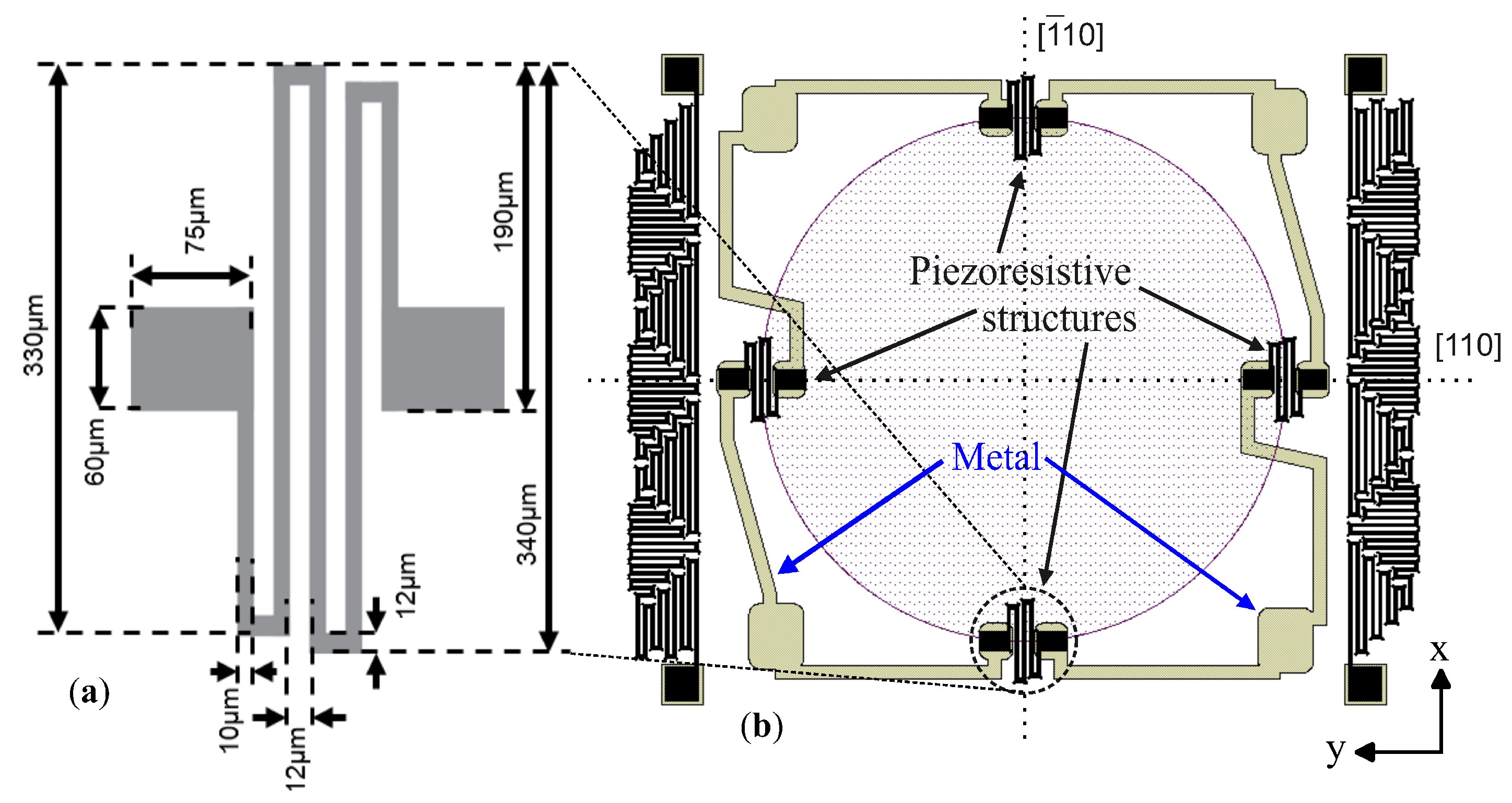
Figure 2.
Layout of the studied temperature sensors. (a) Longitudinal and transverse piezoresistive sections for the cancellation of piezoresistance due to stress and (b) only longitudinal sections.
Figure 2.
Layout of the studied temperature sensors. (a) Longitudinal and transverse piezoresistive sections for the cancellation of piezoresistance due to stress and (b) only longitudinal sections.
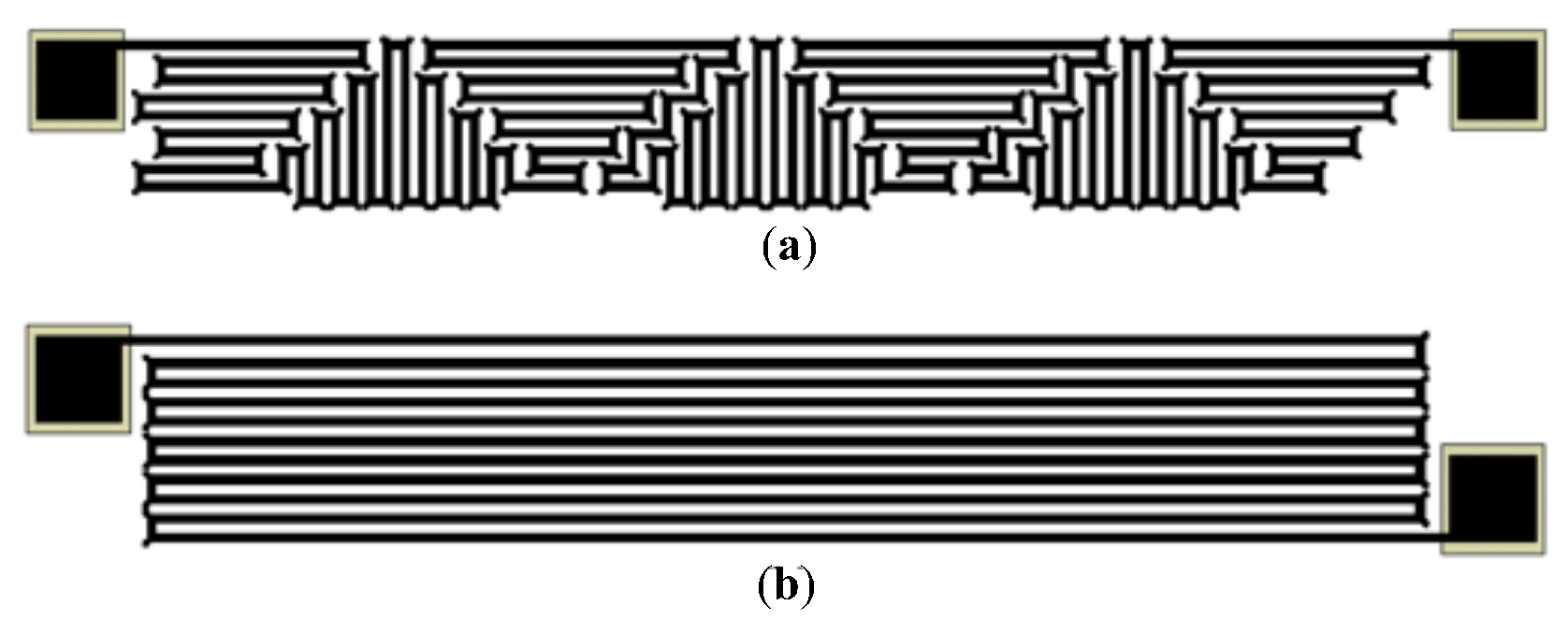
Figure 3.
Fabrication steps for MEMS pressure and temperature sensors.
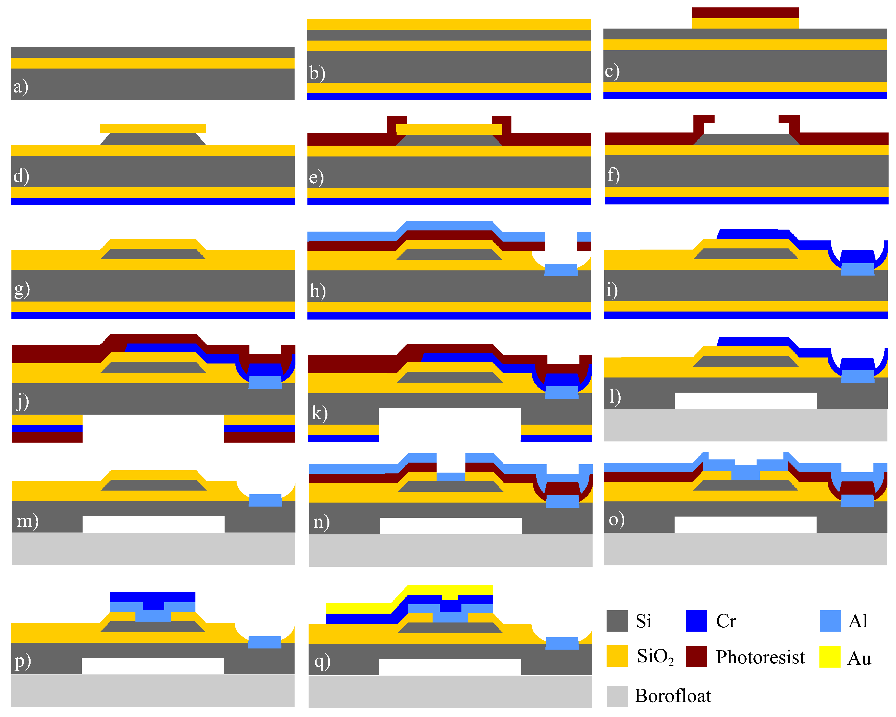
Figure 4.
Finite element simulation results for the membrane. (a) Maximum Von Mises stress for various membrane thickness values as a function of applied pressure. (b) Top and (c) bottom Von Mises stress distributions for a circular membrane with a diameter of 1550 m, a thickness of 190 m, and applied pressure of 70 MPa.
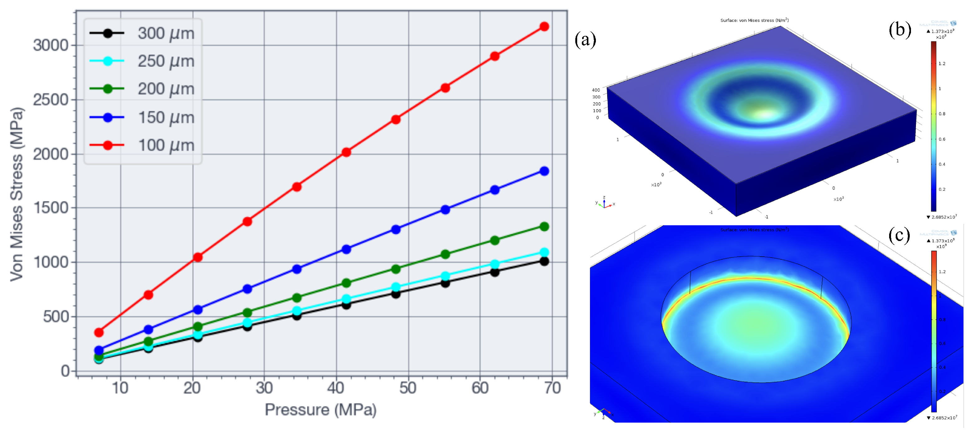
Figure 5.
Finite element simulation of temperature resistors. (a) Membrane under 70 MPa of pressure with the resistor structures shown in Figure 2(a) and Figure 2(b). (b) Comparison of the percentage of change in the piezoresistance value between both designs due to the top membrane stresses as a function of the distance from the membrane edge.
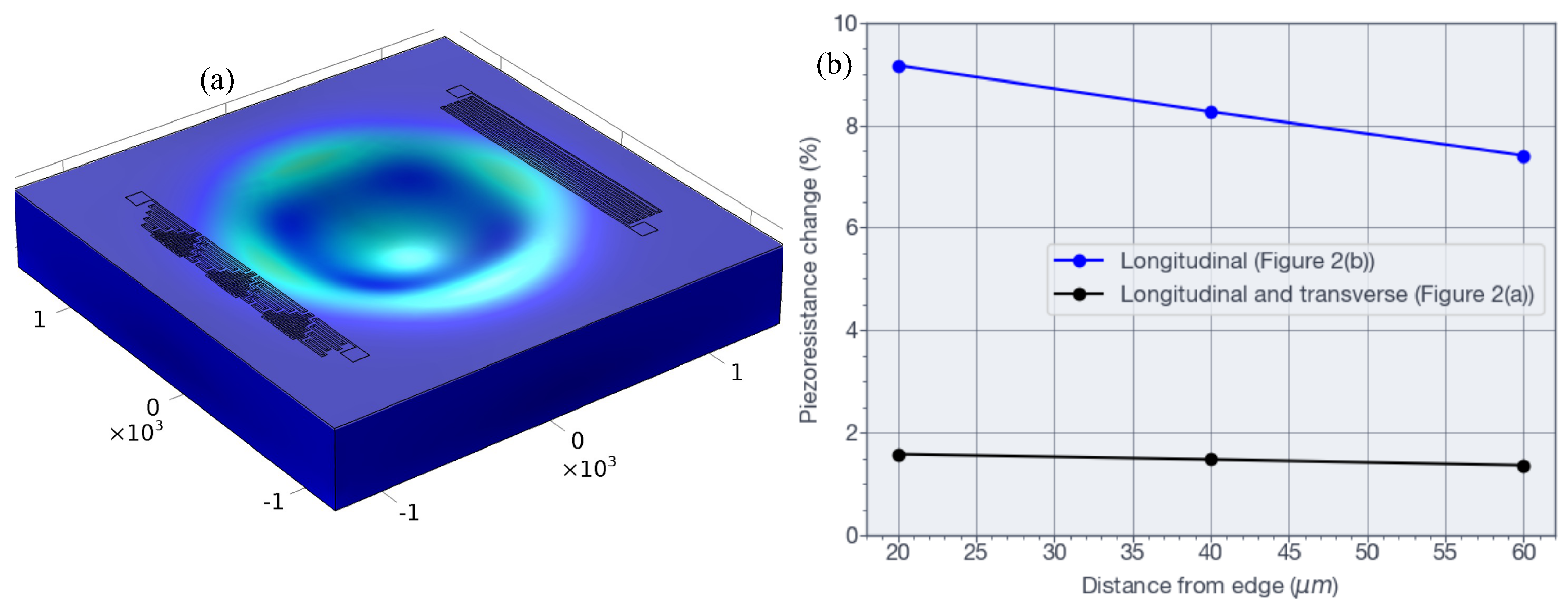
Figure 6.
(a) Complete layout design, including the four pressure piezoresistors and four temperature resistors. (b) Cross section of the supportive structure showing the BOX openings. (c) Cross section of the piezoresistor and bonding support structure.
Figure 6.
(a) Complete layout design, including the four pressure piezoresistors and four temperature resistors. (b) Cross section of the supportive structure showing the BOX openings. (c) Cross section of the piezoresistor and bonding support structure.
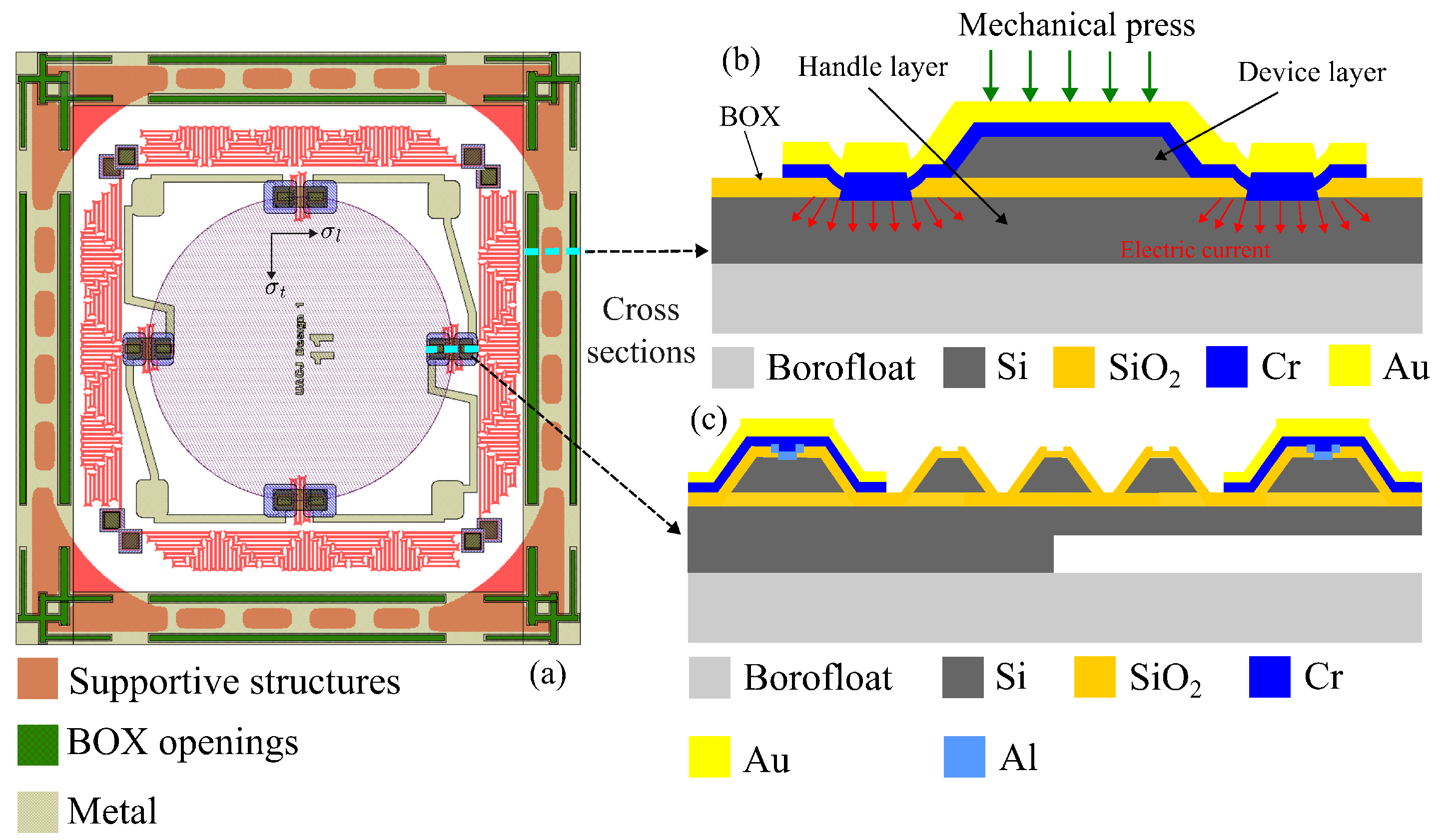
Figure 7.
MEMS sensor fabricated. (a) Top view of pressure and temperature sensors. (b) Perfilometer image showing supportive structure used for bonding the SOI and Borofloat wafers. (c) Four dies wire bonded into a 48 pin dual in line package.
Figure 7.
MEMS sensor fabricated. (a) Top view of pressure and temperature sensors. (b) Perfilometer image showing supportive structure used for bonding the SOI and Borofloat wafers. (c) Four dies wire bonded into a 48 pin dual in line package.
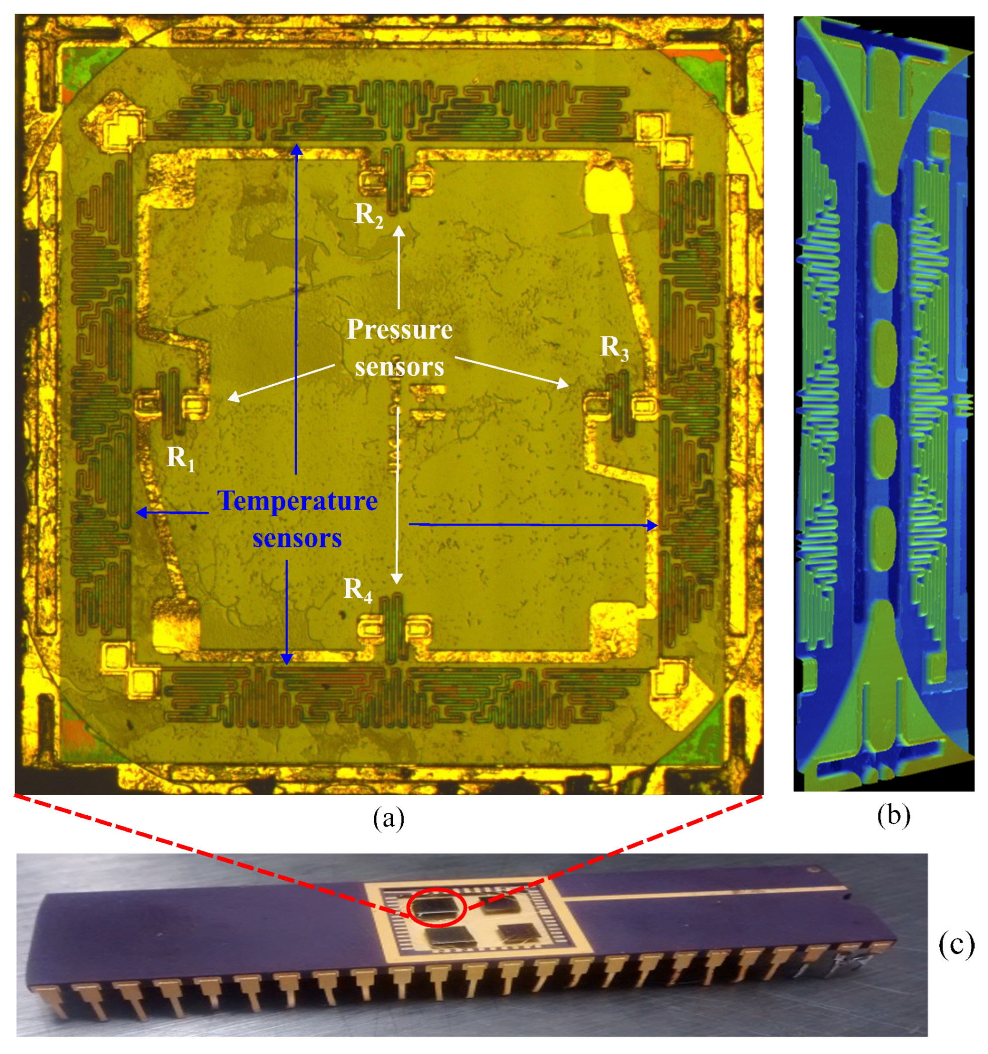
Figure 8.
Low cost setup used in the characterization of pressure and temperature sensors.
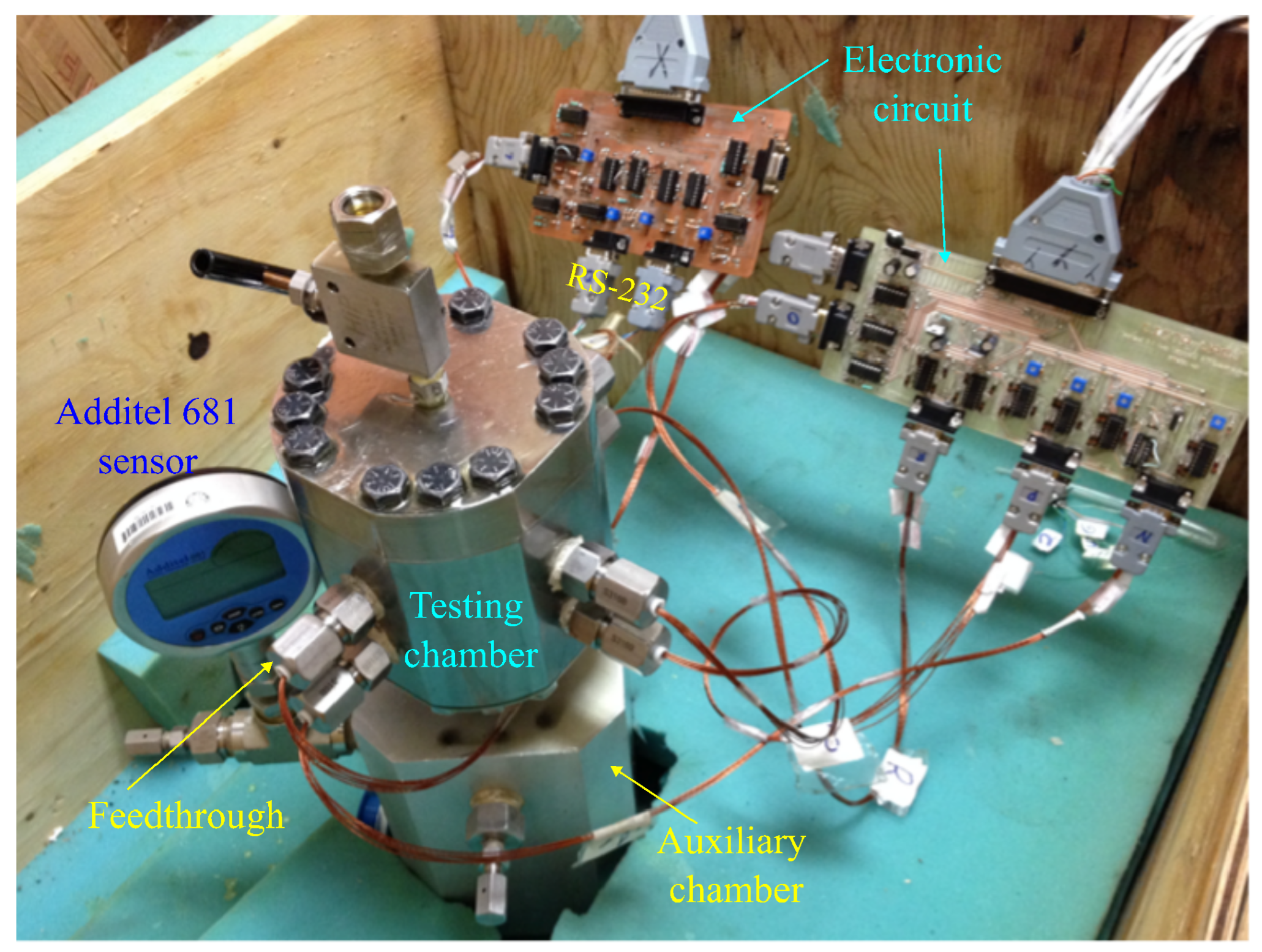
Figure 9.
Customized designed chambers for high pressure testing. (a) Simplex piston cylinder for fluid isolation below the auxiliary chamber, (b) high pressure testing chamber showing four of eight feedthrough connectors, (c) finite element simulation results from stainless steel testing chamber, (d) cross section of testing chamber showing autoclave high pressure connectors, and (e) machined testing chamber showing internal cavity for sensor placement.
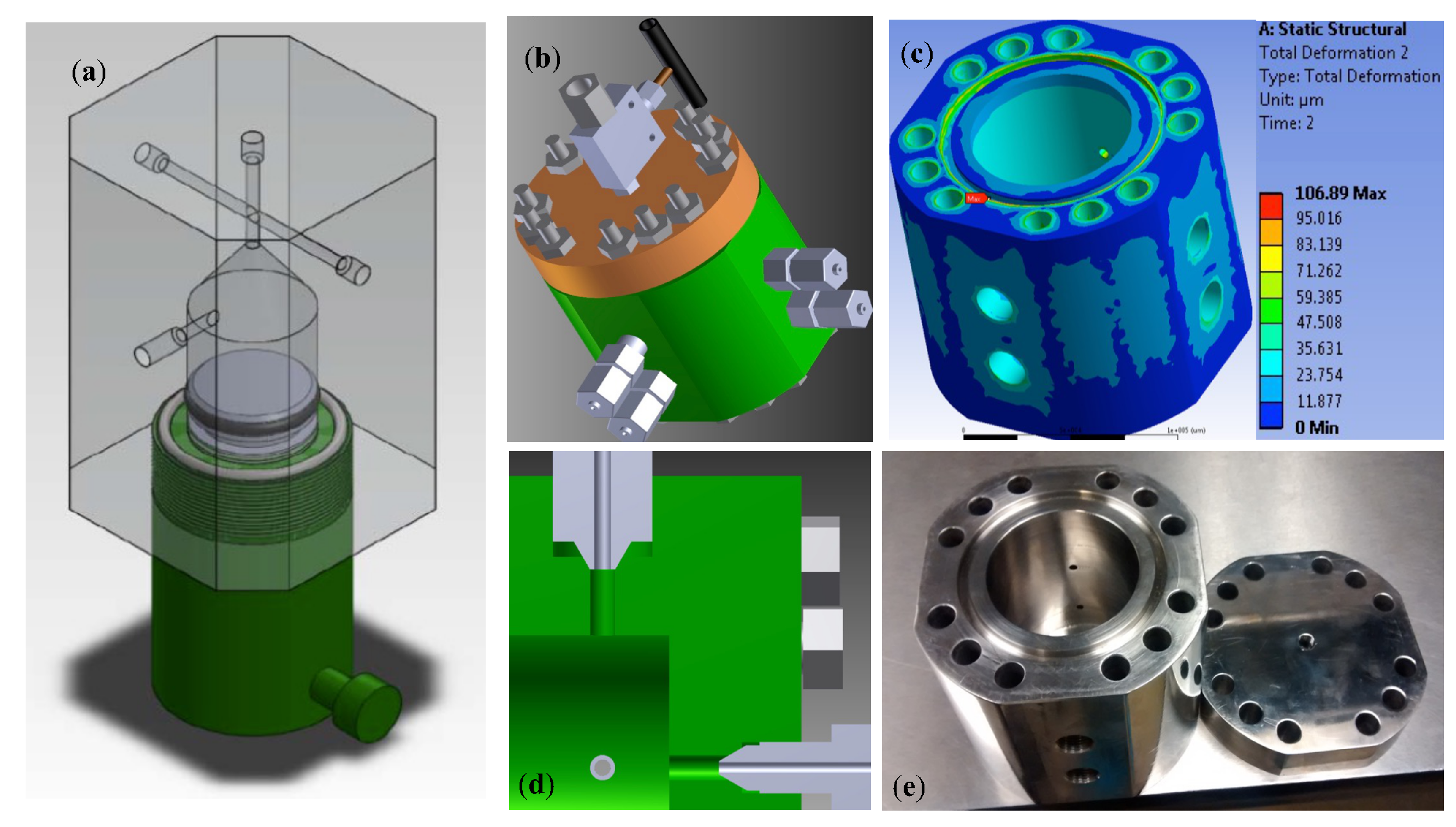
Figure 10.
Electronic circuit used for the calibration and reading of the pressure sensor signals.
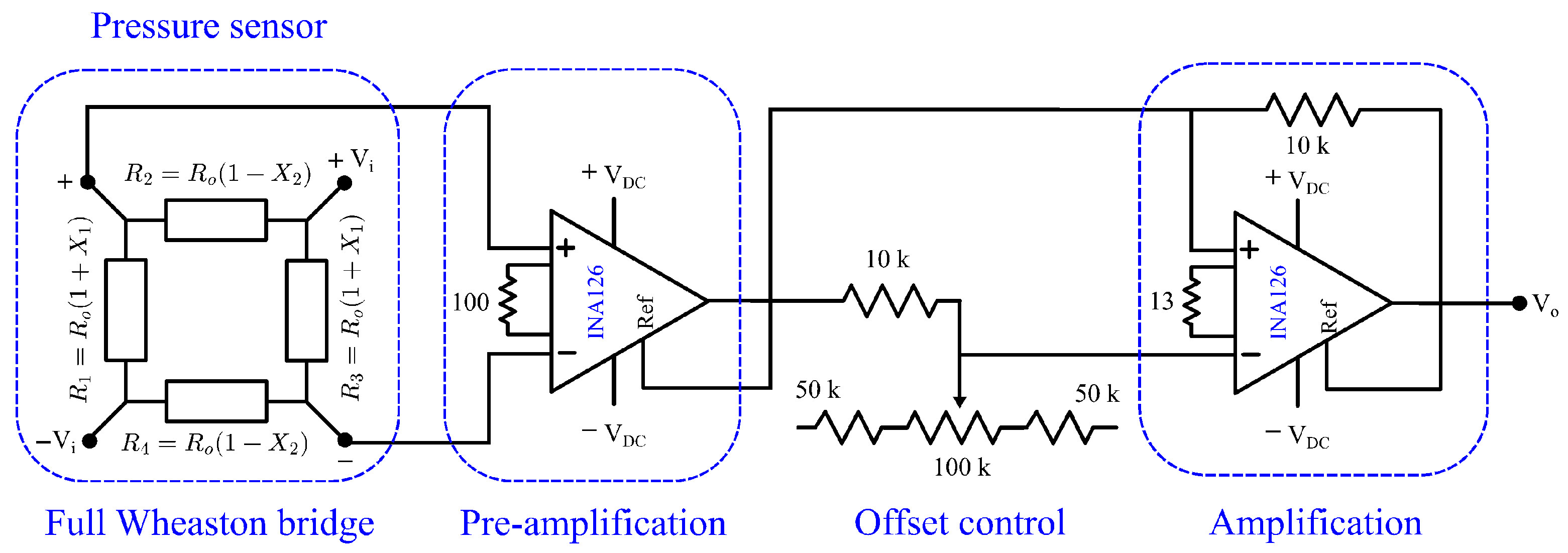
Figure 11.
Output voltaje of pressure sensor after signal conditioning and amplification as function of pressure.
Figure 11.
Output voltaje of pressure sensor after signal conditioning and amplification as function of pressure.
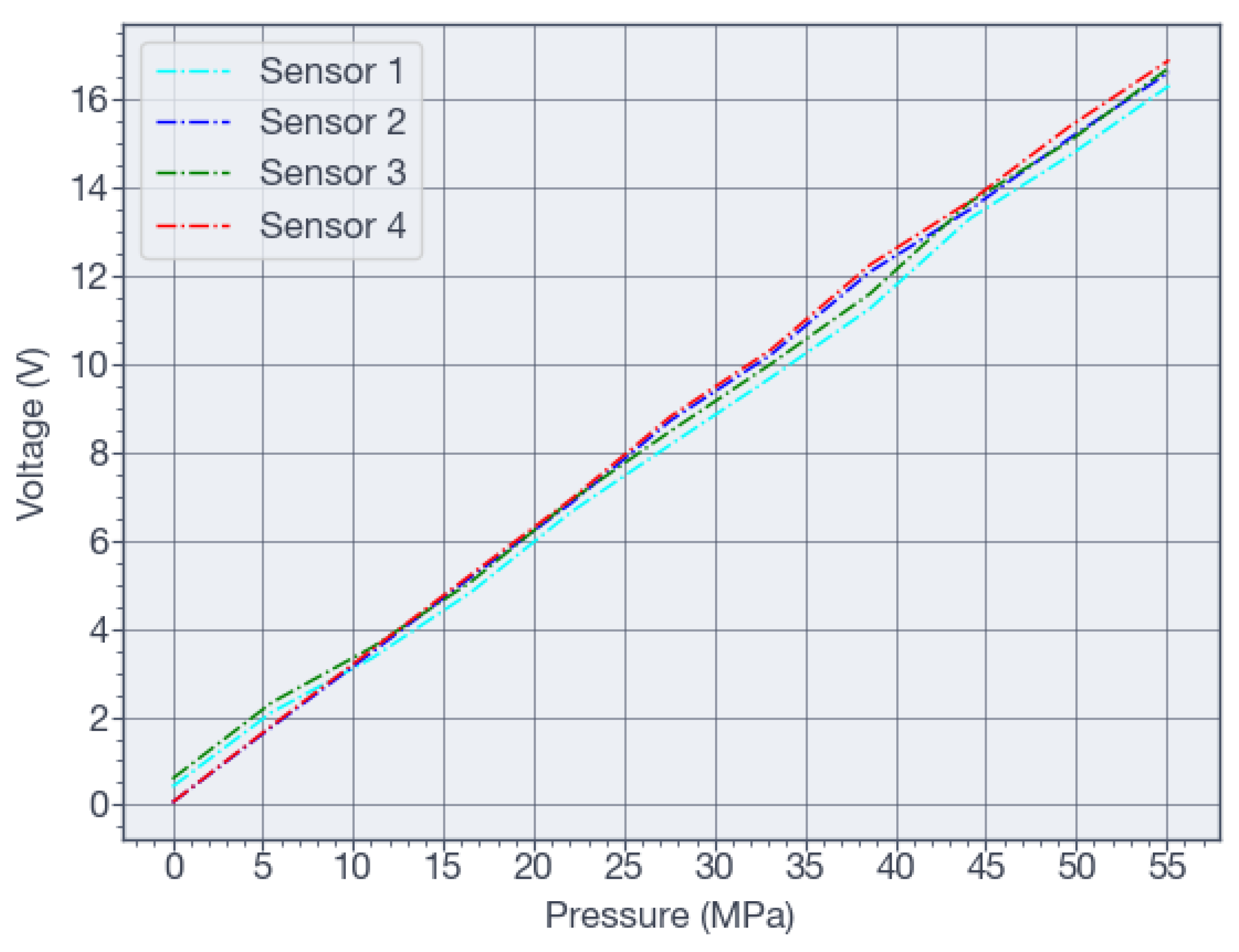
Figure 12.
Resistance as function of temperature measured by four temperature sensors.
Disclaimer/Publisher’s Note: The statements, opinions and data contained in all publications are solely those of the individual author(s) and contributor(s) and not of MDPI and/or the editor(s). MDPI and/or the editor(s) disclaim responsibility for any injury to people or property resulting from any ideas, methods, instructions or products referred to in the content. |
© 2026 by the authors. Licensee MDPI, Basel, Switzerland. This article is an open access article distributed under the terms and conditions of the Creative Commons Attribution (CC BY) license (http://creativecommons.org/licenses/by/4.0/).
Copyright: This open access article is published under a Creative Commons CC BY 4.0 license, which permit the free download, distribution, and reuse, provided that the author and preprint are cited in any reuse.


