
Submitted:
02 February 2026
Posted:
03 February 2026
You are already at the latest version
Abstract
Sine and cosine wave synthesis is utilized for generating sinusoidal-alike values in the digital domain. While this task is commonly handled through software, dedicated hardware like Direct Digital Synthesis (DDS) is also available. However, both methods rely on memory resources, such as look-up tables and Read-Only Memories (ROMs), which face latency limitations related to additional memory access times on top of additional Si area. With the advent of real-time arithmetic for sine wave approximation, this paper presents a digital module that employs iterative multiply-accumulate (MAC) operations for sine and cosine synthesis, ready to be integrated in Systems-on-Chip (SoCs), Field Programmable Gate Arrays (FPGAs), or even standalone Application-Specific Integrated Circuits (ASICs). When implemented on a Xilinx (AMD) XC7A100T-3CSG324 FPGA, the proposed architecture compared to other ROM-less solutions like Taylor approximation, achieves 80.80% lower resource utilization, 80.89% reduced propagation delay, and 36.66% higher accuracy in sine and cosine wave approximation, both operating as 32-bit systems with one sample per clock cycle. Furthermore, the proposed sine accelerator, accompanying control and communication IPs, and custom firmware were deployed on an FPGA-based function generator platform and experimentally validated.
Keywords:
sine wave
; cosine wave
; horner scheme
; polynomial approximation
; digital controller
; FPGA
; waveform synthesis
; hardware acceleration
; function generation
1. Introduction
Sinusoidal waves can be found in applications such as touch screen controllers [1], electromagnetic interference (EMI) cancellation in power electronics [2], software-defined radio, inverters, radar systems, 3D graphics acceleration, instrumentation and signal processing [3,4]. A common application of sinusoidal wave generators is to provide excitation bursts in the kHz and MHz range to perform sensor characterization [5]. Other systems employ sinusoidal waves in motor control applications with Hall sensors [6].
Sine wave generation is a task that most basic applications are solving with software implementations of lookup tables in the memory of a microcontroller which feed data into digital-to-analog converters (DACs) or Pulse Width Modulation (PWM) drivers through Direct Memory Access (DMA) peripherals [7]. The synthesis of sinusoidal functions can also be performed through hardware systems, that can be either fully analog [8] or digital-based circuits [1] to generate the desired sinusoidal waveform.
Commonly used software-based solutions, along with digital circuits based on the Direct Digital Synthesis (DDS) technique, require either lookup tables (LUTs) or Read-Only Memories (ROMs) [9]. The additional data storage circuitry significantly affects function generation latency due to the slow nature of memory access operations and incurs costs associated with the high silicon area required when handling large volumes of data. The data volume problem generated by LUTs and ROMs is based on two limitations - memory depth and memory width. First, achieving a high fidelity signal requires storing more sample points in the memory, which increases the depth of the memory. For instance, 16384 values have better time resolution than 1024, but the address bus width required is 16 bits instead of 10. Secondly, improving the precision of each sample involves increasing the number of bits for the data stored in the memory, which expands the width of the memory. A 16 bit value yields a quantization error of 30.517 ppm, while a 24 bit value offers a quantization error less than 0.12 ppm.
To address the area and latency limitations, ROM-less digital circuits that utilize real-time computation through the implementation of various algorithms have emerged [10]. These architectures use multiple complex circuits such as multipliers and dividers that require large area and significantly increase the total propagation delay between the input data and the synthesized function output.
This work extends [11] and presents a new real-time computation approach in the sense of utilizing the same multiplier and adder in an iterative manner (thus achieving area reduction) in order to generate a high precision sine wave approximation. Moreover, the accelerator was integrated into a FPGA-based function generation system, featuring additional digital IPs for communication (UART) and overall system control, i.e., a FSM, and register access for configuration and accelerator output. Furthermore, a custom firmware framework was developed to manage the FPGA board, to drive the 50 MS/s DAC PCB, and interface with an oscilloscope for experimental validation.
To assess the performance of the proposed work regarding area, latency, and accuracy, a figure of merit was defined that integrates all three metrics. Compared to the best out of the referenced implementation, Taylor approximation, this work shows an improvement of 80.80% in terms of area, 80.89% for propagation delay, and 36.66% higher accuracy for a 32-bit sine and cosine wave approximation design.
Section 2 presents the numerical and mathematical background with respect to the approximation of the sine waves in hardware. Section 3 presents the architecture of the proposed accelerator. Section 4 presents the FPGA-based sine generator in a real-world application scenario. Section 5 presents the accelerator’s performance in terms of area, speed and precision, along with a comparison against other hardware implementations. To evaluate the accelerator’s performance inside the FPGA-based sine generator, real-world measurements are also presented. Finally, the paper ends with concluding remarks in Section 6.
2. Background
This section presents methods for synthesizing sine and cosine waveforms. It also analyzes the implications of the approximation scheme employed in the proposed hardware solution, focusing on reducing the complexity of binary multiplication circuitry and evaluating the precision of the approximation methods.
2.1. Digital Synthesis of Sinusoidal Waves
In applications that require ROM-less hardware acceleration for sine wave generation [1,2,3,4,5,6], various methods for synthesizing sinusoidal waves exist, such as Taylor Series expansion [4,12], Bhaskara approximation [13], and Parabolic Synthesis [14]. These approaches use dedicated arithmetic circuits such as multipliers and adders, or algorithms such as CORDIC [4,15]. However, each method is latency and physical resources required limited, such as LUTs for FPGAs or die area in ASICs.
Bhaskara approximation relies on dividing two polynomials [13]. The division circuitry is known to be complex, hence requiring significant logic resources, while the two polynomials are constructed using multipliers and adders.
Taylor Series and Parabolic Synthesis approximate the sine wave through multiplication, addition, and subtraction [4,10,12,14], thus avoiding division, hence becoming more efficient in terms of area and speed than Bhaskara. The Taylor Series implementation can be scaled for precision by increasing the number of coefficients or employing pipelining to enhance throughput [4]. However, all three methods, i.e., Taylor Series, Parabolic Synthesis, and Bhaskara approximation, demand multiple blocks with dedicated multiplication circuitry, hence requiring significant hardware resources.
2.2. Polynomial Approximation of Cosine Using Horner’s Polynomial Scheme
When looking for a different solution outside of Parabolic Synthesis, Bhaskara or Taylor Series for sinusoidal function approximations, one can take the approach of polynomial approximations through the Horner scheme, which is described in a generic form in Equation 1. By repeatedly factoring the polynomial until we reach the highest power, an iteratively-computable structure can be observed. This structure is particularly well-suited for software or resource-constrained hardware implementations.
The Taylor Series approach can be implemented using Equation 2 following the same method as in Equation 1. Horner’s polynomial scheme for the cosine function utilizes only even powers of x, unlike the sine function that requires both x and . To minimize the average error across the quadrant, a sixth-degree polynomial approximation is implemented using Horner’s method (Equation 2) with the coefficients from Table 1[16]. If a sine wave is desired, one may simply adjust the phase of the data since the sine wave is ahead of the cosine wave by .
The function defined by Equations 1 and 2 is implemented iteratively using Algorithm 1. The algorithm first pre-calculates and stores the value of . The computation is initialized with the highest-order coefficient, . Each subsequent step multiplies the result of the previous iteration by and adds the next coefficient, continuing until all coefficients have been processed.
| Algorithm 1:Iterative Horner approximation algorithm |
whiledo
end while
|
Figure 1 compares the approximation errors of the Bhaskara (red), Taylor Series (blue), and the proposed Horner’s polynomial (green) methods for generating a sinusoidal wave from 0 to . The traces reveal that while the Taylor Series is more accurate in the lower half of the quadrant, the proposed Horner-based method provides a more evenly distributed error. Given the logarithmic Y scale, the Horner-based method uniform error distribution results in a lower average error across the entire quadrant, confirming the numerical analysis presented in [16].
2.3. Symmetry Around and Quadrant Orientation
The proposed accelerator is based on an algorithm that is fundamentally valid for angles within the first quadrant, [0, ]. This design choice is justified by the inherent periodicity and symmetry of sinusoidal functions, as shown in Equation Section 2.3. By mapping any given input angle to its equivalent in the first quadrant and applying the appropriate sign, the accelerator can compute the function over its entire domain. Although the core computation approximates the sine function, the system produces the cosine by incorporating the necessary phase shift.
2.4. Number Format and Precision
The overall precision of the hardware accelerator is constrained by both the approximation method and the fixed-point numerical representation. As with methods like Taylor, Bhaskara or CORDIC, the width of the data bus and the allocation of fractional bits directly influence Horner-based method accuracy due to truncation errors from hardware-level arithmetic like additions, subtractions and multiplications. The proposed cosine synthesizer addresses this by featuring scalable precision, enabling user-configurable parameters for data width and fractional bits for a direct trade-off between resource utilization and precision.
The fixed-point representation uses integers for arithmetic operations while interpreting them as fractions. The position of the fractional point determines the power of 2 represented by the fractional bits, as shown in Equation 4.
The fixed-point representation offers flexibility in selecting the number of fractional bits (m) and integer bits (n) within a fixed data bus size. Figure 2 illustrates the precision improvements achieved by increasing the number of fractional bits for the implementation described in this work and also shows that after 14 bits there is no further precision improvement.
3. Proposed Cosine Synthesizer Based on Horner Polynomial Scheme
Horner’s polynomial approximation not only delivers optimal accuracy with respect to the average approximation error, but also enables the iterative use of a single multiply-accumulate (MAC) circuit, resulting in a latency of only 4 clock cycles for computing a cosine value [11]. Higher orders enhance precision, but incur extra latency from the additional MAC operations needed for each new even power and coefficient. Thus, weighing the accuracy/latency trade-off, for this work, a sixth-degree polynomial approximation was selected. Furthermore, this section describes the design and operation of the proposed cosine wave synthesizer.
3.1. The Cosine Synthesizer Core
The proposed design utilizes a single MAC unit with multiplexed inputs to iteratively generate a new approximation each clock cycle, managed by a finite state machine (FSM). In the first clock cycle, the value is calculated, followed by three MAC operations that leverage the result from the preceding cycle. Figure 3 depicts the internal structure of the cosine synthesizer, excluding the FSM, clock, enable, and reset signals. Initially, the multiplier computes . The second step involves multiplying by the coefficient and adding . The third and fourth (final) steps consist of multiplying the previous iteration’s result by and adding the respective coefficient. In the final cycling stage, the VALID flag is asserted, signaling downstream logic to capture the synthesizer’s output.
3.2. Interleaving Cosine Synthesizer Cores
If the system integrating the synthesizer requires a latency of only one clock cycle, four instances of the proposed design can operate in parallel with interleaved execution and multiplexed outputs, as illustrated in Figure 4. The signal behavior of these four parallel cores is shown in Figure 5.
Each clock cycle, one core outputs a cosine value determined by the input angle. With a latency of four clock cycles per core, the outputs of the four cores are multiplexed to ensure that only one core has a valid output at any given time. Consequently, the initial cosine value is produced after four clock cycles, followed by a new value generated at each subsequent cycle.
Using the aforementioned implementation, the quad-core system streams a new value after each cycle, improving the throughput from 4 cycles/sample to 1 cycle/sample. Input demultiplexing and output multiplexing do not yield significant latency penalties. The main limitation regarding the clock’s top speed is the multiplier architecture, and this is a fixed constraint, due to the fixed DSP48E1 slices in the FPGA chip.
4. Validation Environment
For experimental validation, the proposed accelerator core was integrated into a complete FPGA-based function generation platform, as depicted in Figure 6. The system is controlled by a host computer running custom scripts that issue commands to the FPGA via a serial interface. The accelerator generates digital samples, which are converted to an analog signal by a high-speed DAC on a custom PCB. The resulting analog waveforms are then captured and validated using an oscilloscope.
To enable a versatile and intuitive validation process, a custom communication protocol was developed to manage the interaction between a host computer and the FPGA-hosted accelerator. This protocol allows the computer to send commands over a USB-to-UART serial link, which is facilitated by an on-board bridge. On the FPGA, a dedicated module decodes these commands to dynamically update the accelerator’s configuration registers with the desired values.
4.1. PC Custom Communication Interface
From the computer side, a custom software framework has been developed, providing an abstraction layer that facilitates the configuration of the accelerator system through the functions presented in Table 2.
The first function, dec_to_bin, converts numbers from decimal to the desired fixed point representation, thus offering a more user-friendly configuration of the sine generator. The bin_to_dec is used to convert data from fixed point into decimal in order to display the values read from the function generator more easily. Both functions take as input parameters the value, the number of fractional bits, the number of integer bits and the signed/unsigned number format.
The sine_config function takes as input arguments the desired amplitude, offset, frequency and phase of the analog wave that has to be generated by the accelerator system. The input values for this function are given in decimal, the function calling the dec_to_bin in order to make the conversion. Underneath this function, a set of optimization problems are solved to generate the values of the configuration registers. These optimization problems imply finding the correct system clock division factor and internal counter step to achieve multiple frequencies for the each sample generation.
The control_signal function is used to enable/disable the generator, to change the polarity of the output signal, and to configure the trigger for the shadow buffers of the control registers inside the generator. The trigger can be set to ’none’, or configured to either a period match event or an external trigger signal coming from an input pin of the FPGA.
The read_register and write_register functions allow direct access to the accelerator system’s control registers.
The read_sine_output function can be used to read the accelerator output back to the computer for further processing or plotting.
4.2. FPGA IPs
The FPGA board receives the commands sent from the computer, decodes and executes them. As presented in Figure 7, in addition to the function generation engine, multiple IPs were added, such as the UART module, System Registers and Output Interface.
The Control FSM determines which configuration register needs to be updated and asserts the address bus accordingly. The next step is transferring the received value to the target configuration register on the data bus. The control and configuration finite state machine can either be IDLE, WRITING, READING or DONE, as presented in Figure 8. Upon a reset, the FSM will enter the IDLE state.
When the UART flags that a new byte has been successfully received, the FSM will decode the received byte and execute the appropriate command. If the command implies writing a new register value, the address will be extracted from the command byte. The following bytes contain the data that needs to be written to the designated register. For reading operations, the computer expects to receive the register values, starting with most significant byte from the address that is stored in the command byte.
The configuration registers hold values that are relevant to the behavior of the accelerator system: regular/half wave rectified/full wave rectified sine mode, system clock frequency division factor, angular frequency counter step, amplitude and phase of the output wave. The registers along with the additional circuitry required for the validation of the accelerator system are presented in Figure 9.
The clock division register holds the clock division factor value with respect to the system clock frequency. The clock divider is based on a binary counter and only powers of two are available for the clock division factor.
The angular frequency register holds the magnitude with which the internal counter increases at each positive edge of the clock signal. The phase register holds the start value of the internal counter and determines which of the 4 quadrants the counter starts from.
The counter is limited between values corresponding to the desired signed fixed point representation of 0 and . When the counter transitions between quadrants, the counter’s output is processed so that the accelerator’s input is kept between 0 and , exploiting the symmetry of (co)sine waves, outlined by Equation Section 2.3. The output wave sign is determined based on the current quadrant, the selected alternance mode and applied at the accelerator’s output.
The amplitude register holds an unsigned fixed point value between 0 and 1 that will be multiplied with the output of the accelerator, in order to match the input range of the external DAC chip placed on the PCB. The offset register holds the signed fixed point value that will be added to the output of the multiplication between the amplitude register’s contents and the accelerator’s output.
The output interface block is responsible with formatting the accelerator’s output so that it matches the digital input coding format of the DAC.
4.3. The Custom High Speed DAC Board
The accelerator system hardware implementation consists of two primary components: the previously described FPGA board and a custom-designed PCB for high-fidelity digital-to-analog conversion. The PCB was specifically developed to handle the accelerator’s output, integrating a high-speed, differential current-steering DAC with a parallel digital interface to maximize data throughput. To convert the DAC’s current output into a usable voltage signal, the board also includes an operational amplifier configured as a current-to-voltage (I/V) converter stage. Figure 10 provides a high-level schematic of this interconnected system, illustrating the primary components and signal paths while omitting ancillary circuitry such as power regulators and passive components for clarity.
The system’s maximum operating frequency is constrained to 50 MHz by the 50 MSps sample rate of the chosen DAC. This converter provides a 12-bit resolution via a parallel input interface and generates a differential current output, which is conditioned to produce a final analog signal with a ±5 V range.
5. Results
This section evaluates the proposed sine wave synthesizer in terms of area, speed, and precision. We also report on its experimental validation within an FPGA-based function generator. To facilitate a comprehensive comparison with prior works, we introduce a figure of merit (FoM) derived from these performance metrics.
5.1. Implementation Results
The proposed design is compared with other implementations analyzed in [10], utilizing the same FPGA, the Xilinx (AMD) XC7A100T-3CSG324.
Table 3 presents a comparison of LUT utilization for the proposed design and other literature implementations across for three common data bus widths: 16, 24, and 32 bits. The results clearly demonstrate the superior area efficiency of our proposed single-core implementation. For a 16-bit data path, our design requires only 36 LUTs, which is approximately 5× smaller than the next most efficient method (Parabolic synthesis at 179 LUTs) and over 40× smaller than the Bhaskara-based approach.
This trend of significant area reduction holds as precision increases. At 32 bits, our single-core design consumes only 142 LUTs, representing a reduction of 81% compared to Parabolic synthesis and 97% compared to the Taylor series implementation.
Furthermore, the table includes a four-core version of our design to illustrate its scalability. While the resource usage increases, the four-core implementation remains highly competitive. For instance, at a 32-bit width, it requires 776 LUTs, which is comparable to the Parabolic synthesis method (779 LUTs) but offers the potential for a four-fold increase in throughput. This highlights a key trade-off, allowing for a balance between minimal area for a single-core implementation and high performance for a multi-core architecture, all while maintaining a smaller footprint than conventional CORDIC, Taylor series, or Bhaskara-based solutions at higher bit-widths.
The speed performance of the proposed architecture is evaluated by analyzing the maximum combinational path delay, with results presented in Table 4.
The results indicate that our proposed architecture achieves a shorter critical path delay compared to all referenced designs across all data bus widths. For a 32-bit implementation, our single-core design has a delay of only 12.656 ns, which is 2.7× faster than the most competitive alternative (Parabolic synthesis at 34.462 ns) and over 12× faster than the Bhaskara-based circuit. Hence, this short delay allows our design to be integrated into high-speed systems.
However, a four-cycle latency is required for our single-core design. To address this, the four-core version is presented. This parallel architecture is designed to produce one sample per clock cycle, thereby quadrupling the throughput. Notably, the four-core implementation exhibits a slightly lower combinational delay (e.g., 11.936 ns for 32 bits) than the single-core version due to synthesis tool optimizations across the smaller, more independent parallel paths. This demonstrates that our architecture can be configured for either maximum clock speed with moderate throughput (single-core) or for maximum throughput at a similarly high clock speed (four-core), offering a flexible trade-off between area (as shown in Table 3) and sample generation rate.
To quantify the numerical accuracy, the maximum relative error of the generated sine wave was measured for each implementation. The results, shown in Table 5, were obtained using the evaluation framework described in [10].
The analysis reveals that our proposed architecture achieves a level of precision that is superior to the state-of-the-art. At a 16-bit data width, our design’s relative error of 0.0048% is significantly lower than that of the Bhaskara, CORDIC, and Parabolic synthesis methods, and is surpassed only slightly by the Taylor series implementation. As the data bus width increases to 24 bits, the precision of our design becomes virtually identical to that of the Taylor series method, with both exhibiting a relative error of approximately 0.0003%. At the highest tested precision of 32 bits, our work demonstrates a clear advantage, achieving a relative error of 0.00019%, which is about 37% lower than the 0.0003% error of the Taylor series approach. This shows that the accuracy of our algorithm scales more effectively with increasing bit width than other high-precision methods.
As expected, the precision is identical for both the single-core and four-core implementations, since they execute the same algorithm and only differ in their parallel structure. This result, combined with the area and speed metrics from Table 3 and Table 4, confirms that our design provides top-tier precision without the significant hardware overhead or high latency characteristic of methods like the Taylor series or CORDIC, respectively.
To provide a holistic comparison that balances area, speed, and precision, we define a Figure of Merit (FoM) as depicted in Equation 5, to compare the proposed implementation with those in [10] on the same FPGA fabric.
A lower FoM indicates a more efficient design, as it represents a better trade-off between resource consumption (Area), processing time (Delay), and numerical accuracy (Error). The FoM was calculated for each implementation across 16, 24, and 32-bit data widths, with the results summarized in Table 6 and visualized in Figure 11.
For this analysis, several methodological considerations are important:
- Single-Core Latency: To ensure a fair comparison of throughput, the delay component for our single-core synthesizer was multiplied by four, reflecting its four-cycle latency to produce a new sample.
- CORDIC Reference: The speed for the CORDIC algorithm was not benchmarked in [10] due to its variable latency. Therefore, we conservatively used its minimum (best-case) delay value for this FoM calculation as a reference point.
- Visual Scaling: In Figure 11, the FoM for the Bhaskara implementation was scaled down by a factor of 1000. This was necessary for visual clarity to prevent its significantly larger value from obscuring the comparison between the other, more efficient designs.
The results demonstrate the superiority of our proposed architectures. As shown in Table 6, our single-core implementation achieves the lowest FoM at 16, 24 and 32 bits, outperforming the Taylor series method.
Furthermore, our four-core implementation, which delivers one sample per cycle, establishes a new state-of-the-art in overall efficiency. When compared against the best-performing reference design (Taylor Series), our four-core architecture achieves a superior FoM by 48.2% at 16 bits, 96.6% at 24 bits, and 97.7% at 32 bits. In conclusion, the proposed design offers an excellent trade-off between performance, area, and precision.
5.2. Experimental Validation
For experimental validation, the proposed sine/cosine synthesizer was integrated into an FPGA-based function generator controlled by a PC. The hardware setup, depicted in Figure 12, consists of the FPGA development board hosting the synthesizer and a custom PCB for digital-to-analog conversion. The FPGA board is powered by the host computer, while the analog PCB requires an external ,V supply.
The sine wave synthesizer is configured through commands sent from the PC, and the output of the analog platform is observed and measured using an oscilloscope. All configurations were tested, including regular sine waves, half-wave rectified, and full-wave rectified modes. In addition, different signal parameters such as frequency, amplitude, and offset were adjusted to evaluate the flexibility and performance of the system.
The system’s waveform generation capabilities were validated through a series of tests under diverse parameter configurations. Initially, a standard 1.5 MHz sine wave with a 3 V amplitude and zero offset was generated to establish a baseline (Figure 13). The firmware’s dynamic frequency adaptation was then tested by generating a 1 kHz sine wave with a 2 V amplitude and a +2 V DC offset; this configuration required the firmware to select an optimal clock division factor and angular frequency step (Figure 14). Finally, the system’s non-linear output modes were demonstrated by generating a 3 V half-wave rectified signal (Figure 15) and a 2.5 V inverted full-wave rectified signal (Figure 16).
The waveform generator consistently delivered accurate and stable outputs across a all configurations, including sinusoidal, half-wave, and full-wave rectified signals. Frequency tuning was smooth and effective, demonstrating the system’s flexibility and precise control. These results highlight the reliability and adaptability of the signal generation setup for a wide range of test and measurement scenarios.
6. Conclusions
A new architecture for ROM-less sinusoidal waveform synthesis was presented and implemented. The results of the FPGA implementation were compared with other solutions from literature. A figure of merit has been determined and used for an overall performance evaluation. The comparison shows that this work achieves 80.80% lower resource utilization, 80.89% reduced propagation delay, and 36.66% higher accuracy, when compared to the best existent solution, Taylor approach, both operating as 32-bit systems with with a throughput of one sample per clock cycle. The proposed cosine synthesizer was integrated along with control and communication IPs in a FPGA-based function generator. Custom firmware was developed to configure the function generator and a custom PCB was created for the digital to analog conversion process. The complete system was validated in real-world use cases, with oscilloscope measurements.
Funding
This work was funded from the project "National Platform for Semiconductor Technologies", contract no. G 2024-85828/390008/27.11.2024, SMIS code 304244, co-funded by the European Regional Development Fund under the Program for Intelligent Growth, Digitization, and Financial Instruments.
Abbreviations
The following abbreviations are used in this manuscript:
| ASIC | Application-Specific Integrated Circuit |
| DAC | Digital-to-Analog Converter |
| DDS | Direct Digital Synthesis |
| DMA | Direct Memory Access |
| EMI | Electromagnetic Interference |
| FoM | Figure of Merit |
| FPGA | Field Programmable Gate Array |
| FSM | Finite State Machine |
| IP | Intellectual Property |
| LUT | Lookup Table |
| MAC | Multiply Accumulate |
| PCB | Printed Circuit Board |
| PWM | Pulse-Width Modulation |
| ROM | Read-Only Memory |
| SoC | System on Chip |
| UART | Universal Asynchronous Receiver/Transmitter |
| USB | Universal Serial Bus |
References
- Kim, J.; Mohamed, M. G. A.; Kim, H. Design of a Frequency Division Concurrent sine wave generator for an efficient touch screen controller SoC. 2015 International Symposium on Consumer Electronics (ISCE), Madrid, Spain, 2015; pp. 1–2. [Google Scholar]
- Bendicks, A.; Peters, A.; Frei, S. FPGA-Based Active Cancellation of the EMI of a Boost Power Factor Correction (PFC) by Injecting Modulated Sine Waves. IEEE Letters on Electromagnetic Compatibility Practice and Applications vol. 3(no. 1), 11–14. [CrossRef]
- Baozhong, Xie; Tiequn, Chen. Sine wave algorithm based on 2nd offset and its implementation in FPGA. IEEE 2011 10th International Conference on Electronic Measurement & Instruments, Chengdu, China, 2011; pp. 173–176. [Google Scholar]
- Adiono, T.; Timothy, V.; Ahmadi, N.; Candra, A.; Mufadli, K. CORDIC and Taylor based FPGA music synthesizer. TENCON 2015 - 2015 IEEE Region 10 Conference, Macao, China, 2015; pp. 1–6. [Google Scholar]
- Lutter, K.; Backer, A.; Drese, K.S. Guided Acoustic Waves in Polymer Rods with Varying Immersion Depth in Liquid. Sensors 2023, 23, 9892. [Google Scholar] [CrossRef] [PubMed]
- NXP Semiconductor, Sinusoidal Control of BLDCM with Hall Sensors - Application Note.
- Miller, Alec. AN3312: Arbitrary Waveform Generator Using DAC and DMA; Microchip Technology Inc.
- Revanna, N.; Viswanathan, T. R. Low frequency CMOS sinusoidal oscillator for impedance spectroscopy. 2014 IEEE Dallas Circuits and Systems Conference (DCAS), Richardson, TX, USA, 2014; pp. 1–4. [Google Scholar]
- Strelnikov, I. V.; Ryabov, I. V.; Klyuzhev, E. S. Direct Digital Synthesizer of Phase-Manipulated Signals, Based on the Direct Digital Synthesis Method. In 2020 Systems of Signal Synchronization, Generating and Processing in Telecommunications (SYNCHROINFO); Svetlogorsk, Russia, 2020; pp. 1–3. [Google Scholar]
- Roy, S. Discretized Sinusoidal Waveform Generators for Signal Processing Applications. 2018 2nd International Conference on Trends in Electronics and Informatics (ICOEI); pp. 1350–1353.
- Stoica, F. -G.; Calinescu, A.; Enachescu, M. A High-Speed, Area-Optimized, ROM-Less (Co)Sine Wave Synthesis Accelerator. 2024 International Symposium on Electronics and Telecommunications (ISETC), Timisoara, Romania; 2024, pp. 1–4. [CrossRef]
- BRUNELLI, C; BERG, H; GUEVORKIAN, D. Approximating sine functions using variable-precision taylor polynomials [J]; SiPS; pp. 57–62.
- Nekounamm, M.; Eshghi, M. An efficient ROM-less direct digital synthesizer based on Bhaskara I’s sine approximation formula. 2012 IEEE International Frequency Control Symposium Proceedings, Baltimore, MD, USA, 2012; pp. 1–6. [Google Scholar]
- LI, X J. A Direct digital frequency synthesizer based on two segment fourth-order parabolic approximation [J]. IEEE Transactions on Consumer Electronics vol. 55(no. 2), 322–326. [CrossRef]
- Chinnathambi, M.; Bharanidharan, N.; Rajaram, S. FPGA implementation of fast and area efficient CORDIC algorithm. 2014 International Conference on Communication and Network Technologies, Sivakasi, India, 2014; pp. 228–232. [Google Scholar]
- Schlör, Lasse. Fast MiniMax Polynomial Approximations of Sine and Cosine.
Figure 1.
Sine polynomial approximation error comparison on a logarithmic scale.
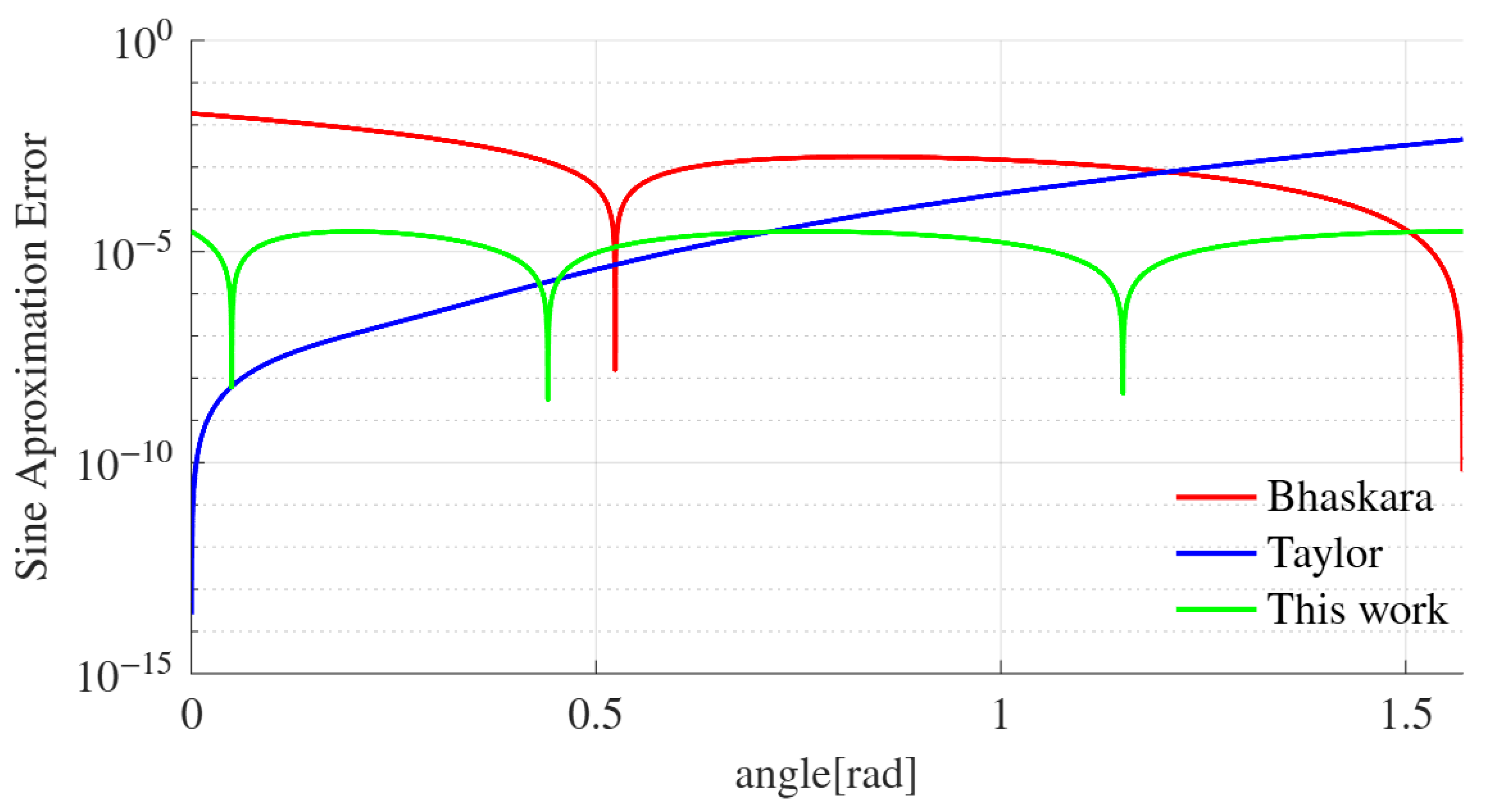
Figure 2.
Average Error of Fixed-Point Implementation vs. Number of Fractional Bits (Top); Precision Saturation after 16 bits (Bottom).
Figure 2.
Average Error of Fixed-Point Implementation vs. Number of Fractional Bits (Top); Precision Saturation after 16 bits (Bottom).
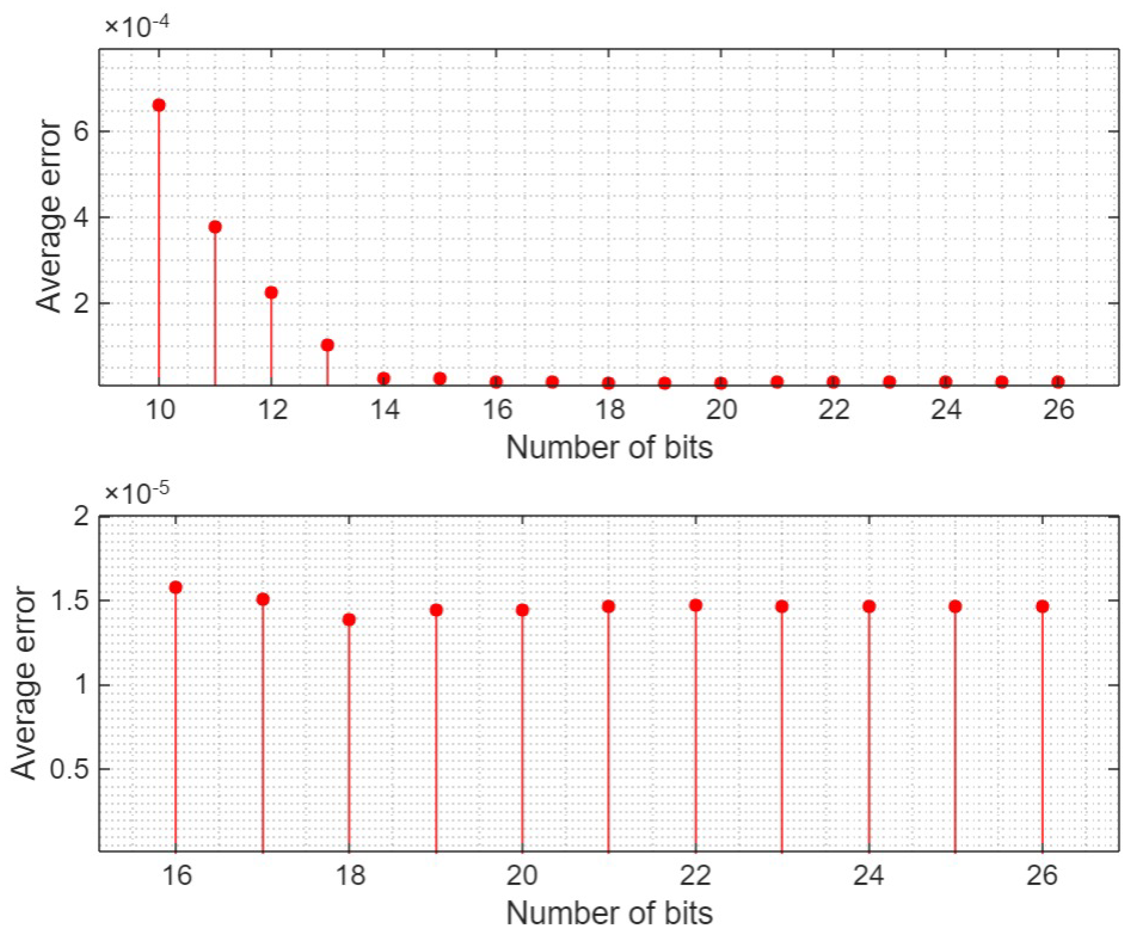
Figure 3.
Internal structure of the iterative cosine synthesizer.
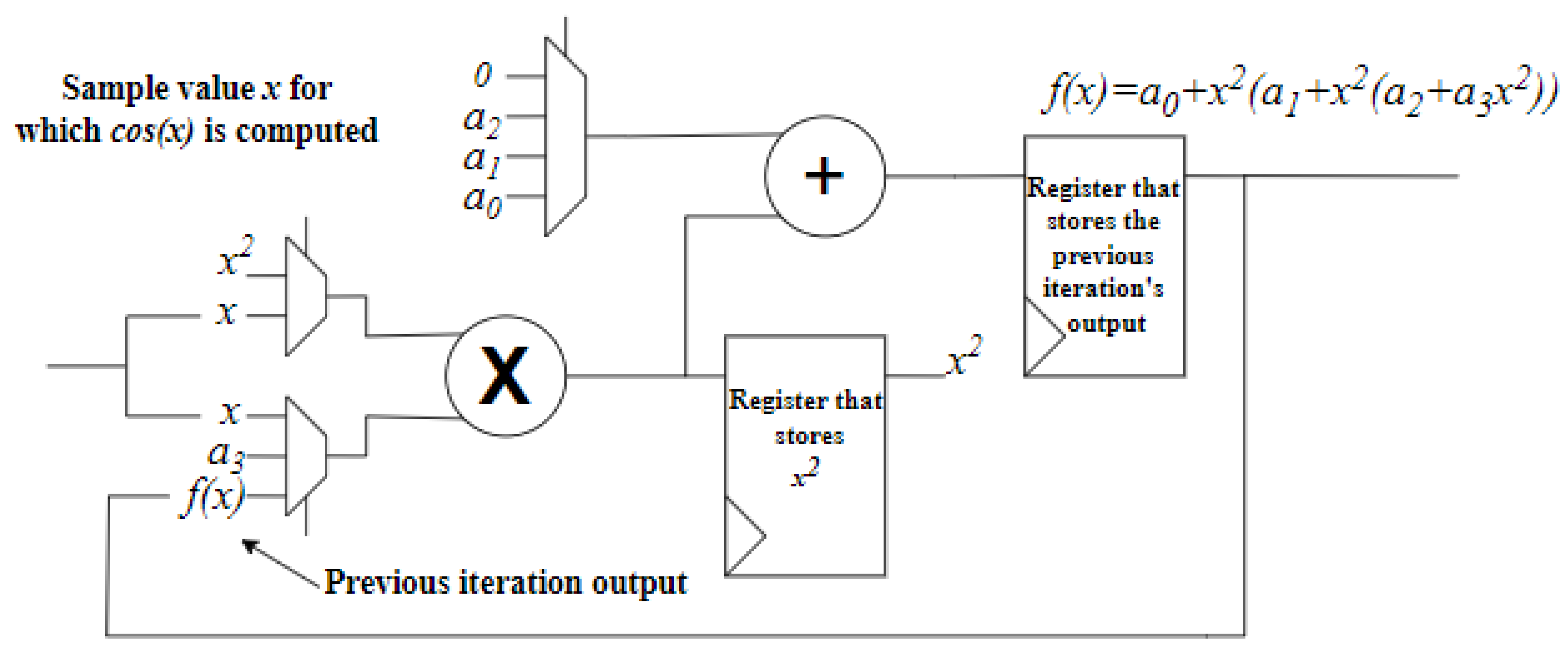
Figure 4.
Achieving one sample per clock cycle by using 4 interleaved cosine synthesizers.
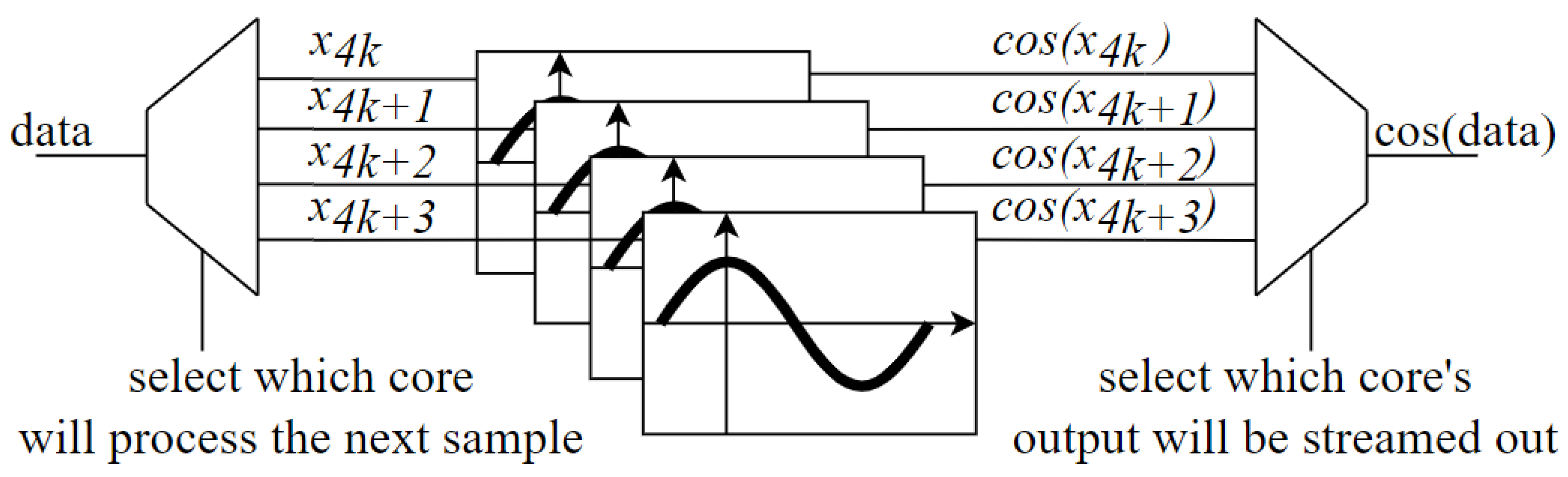
Figure 5.
Timing of outputs of a system built with 4 cosine synthesizers with interleaved activity. Each clock cycle generates a new cosine function output.
Figure 5.
Timing of outputs of a system built with 4 cosine synthesizers with interleaved activity. Each clock cycle generates a new cosine function output.
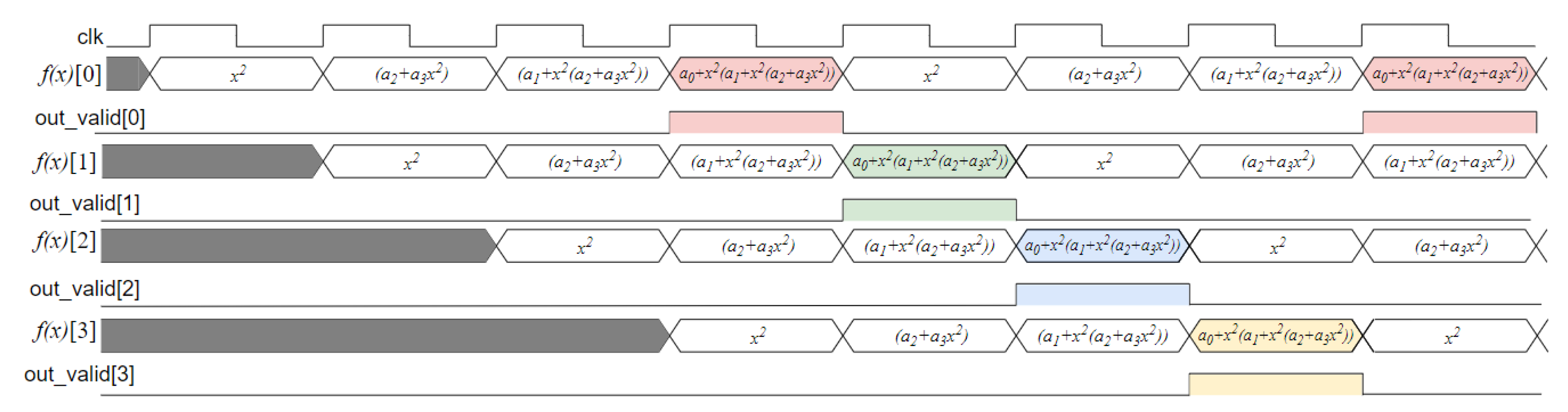
Figure 6.
Validation framework.
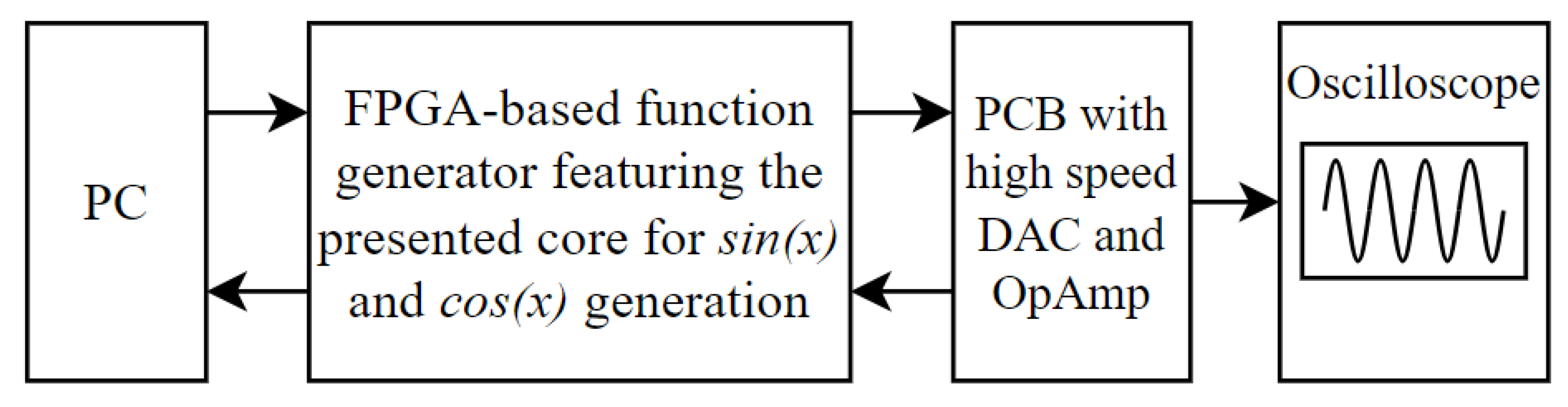
Figure 7.
FPGA IPs.
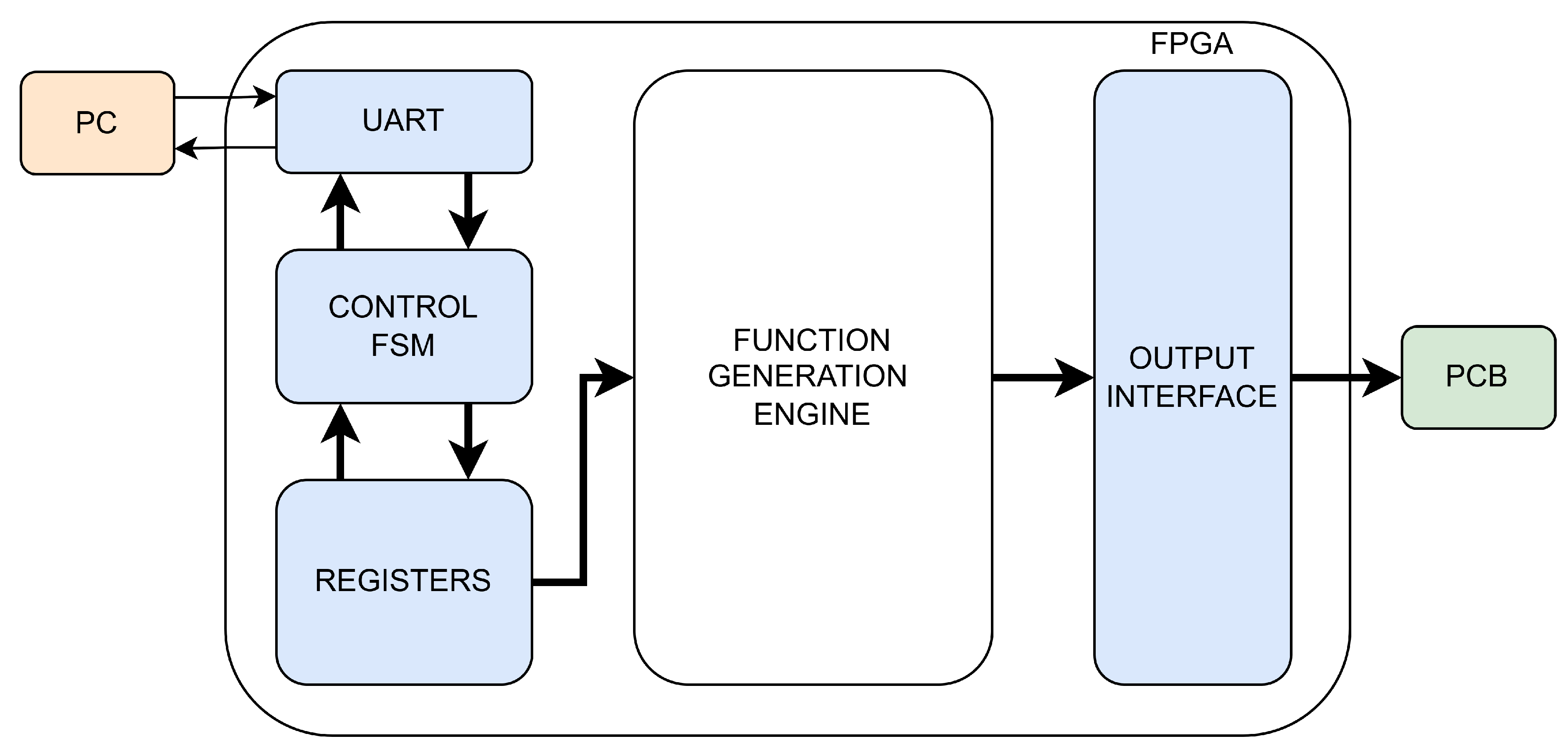
Figure 8.
States of the Control FSM.
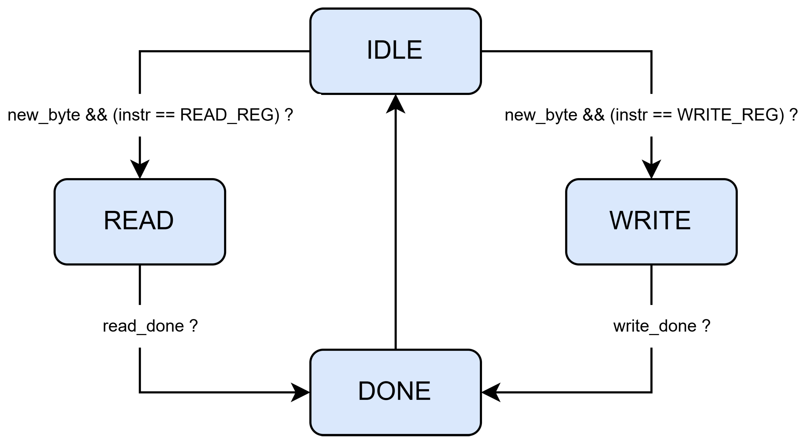
Figure 9.
Accelerator system control registers.
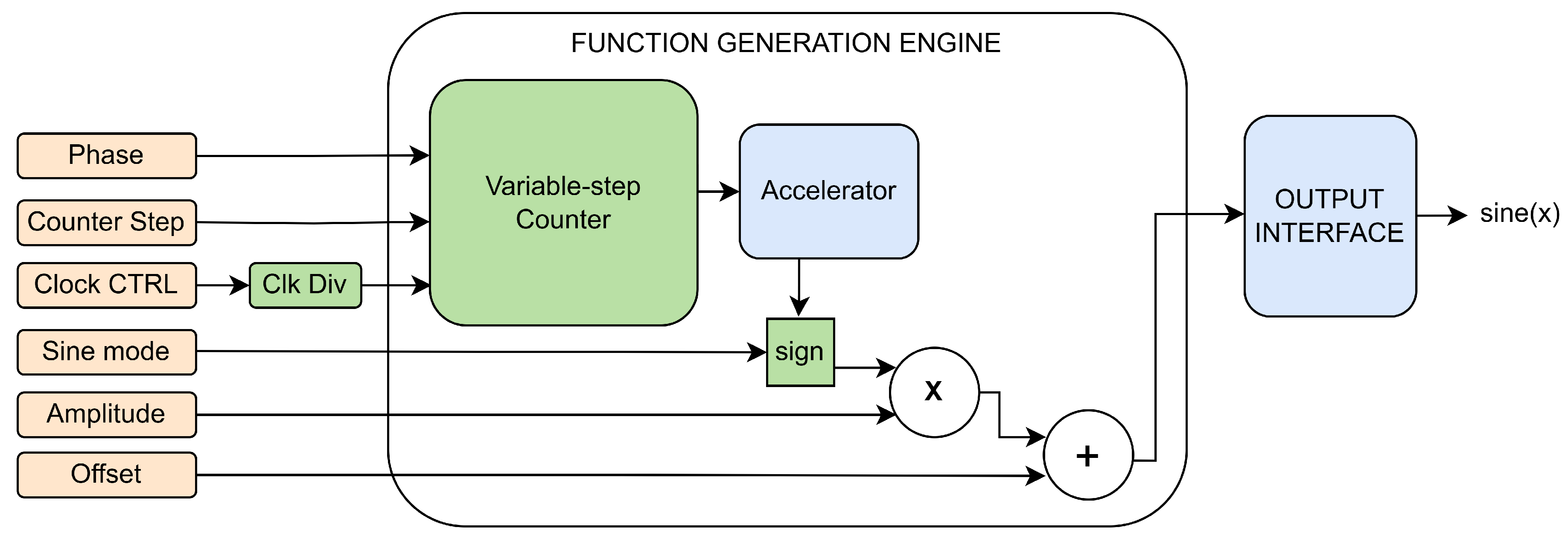
Figure 10.
FPGA and D/A conversion PCB high level schematic.
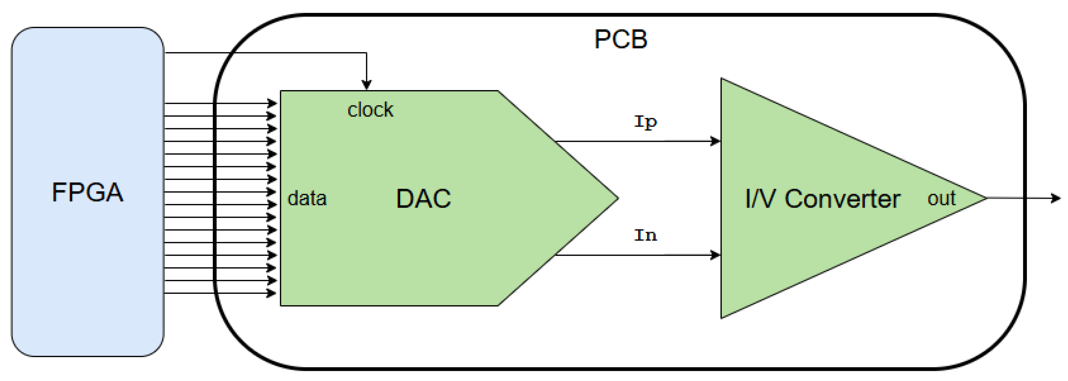
Figure 11.
Figure of Merit bar graph.
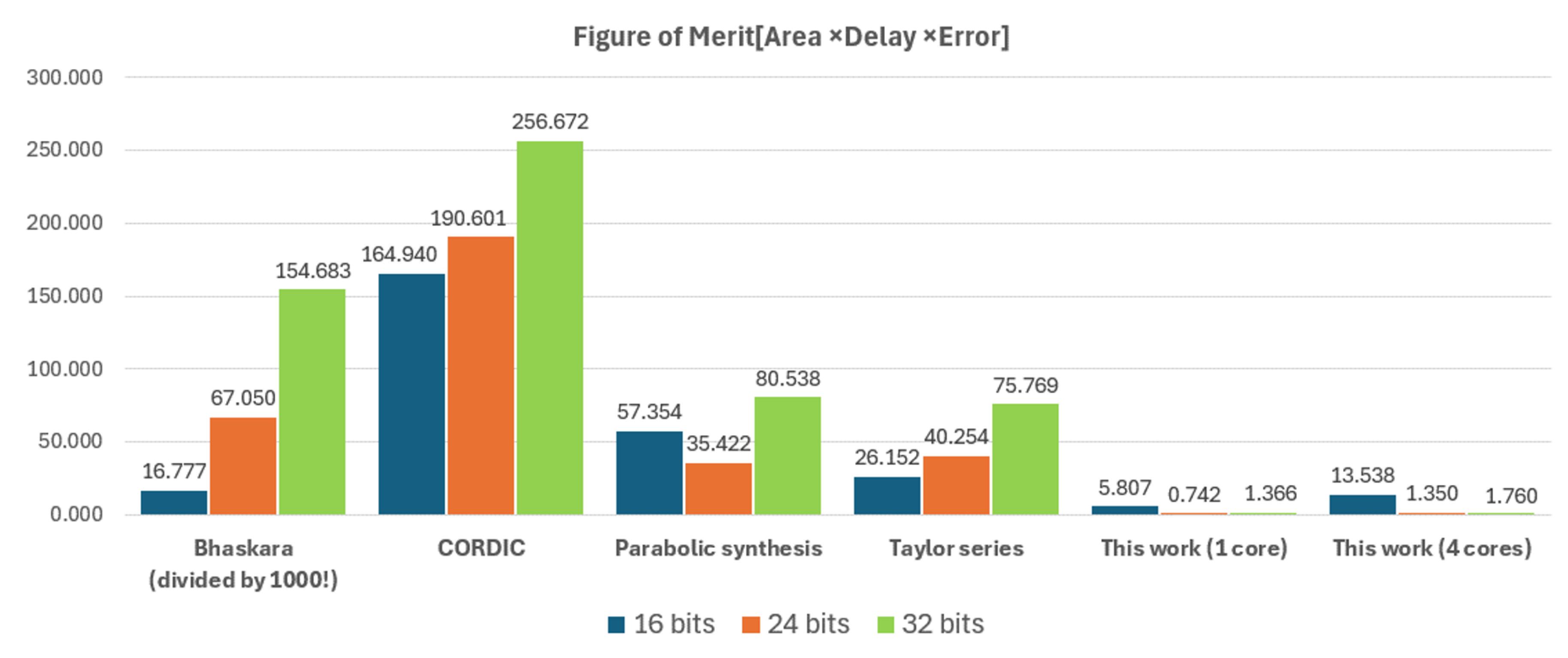
Figure 12.
Validation boards.
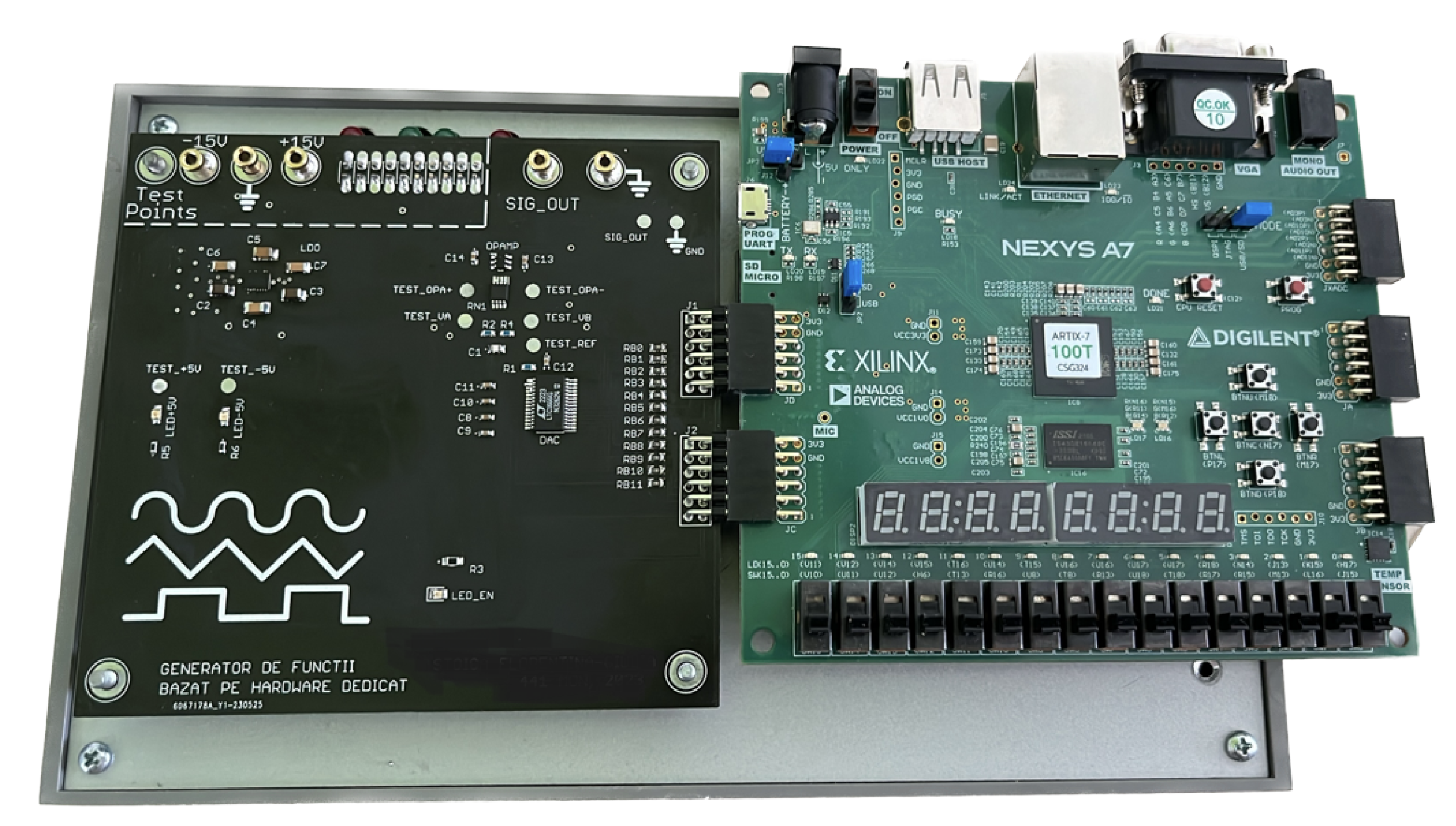
Figure 13.
Regular sine:
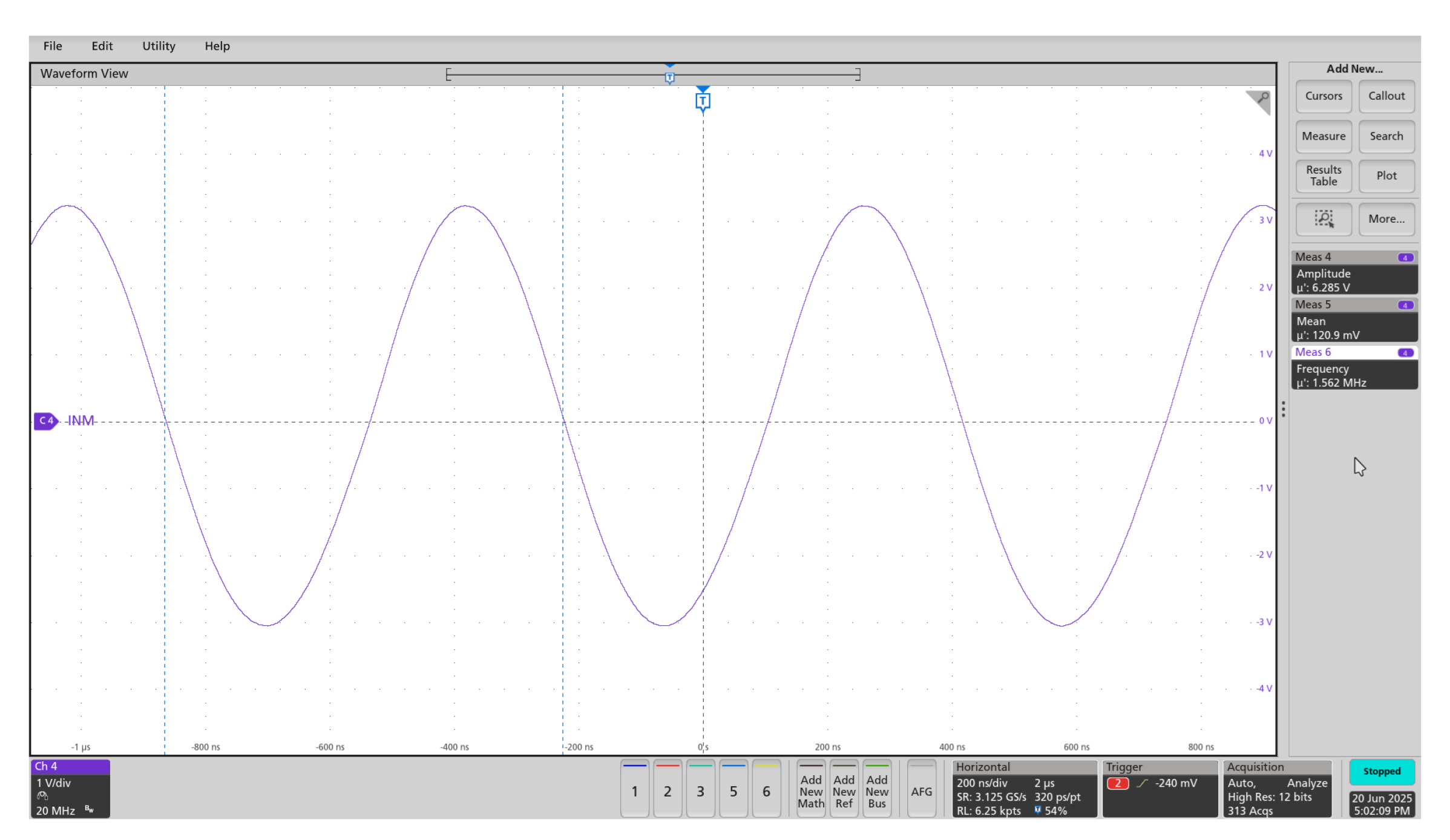
Figure 14.
Regular sine:
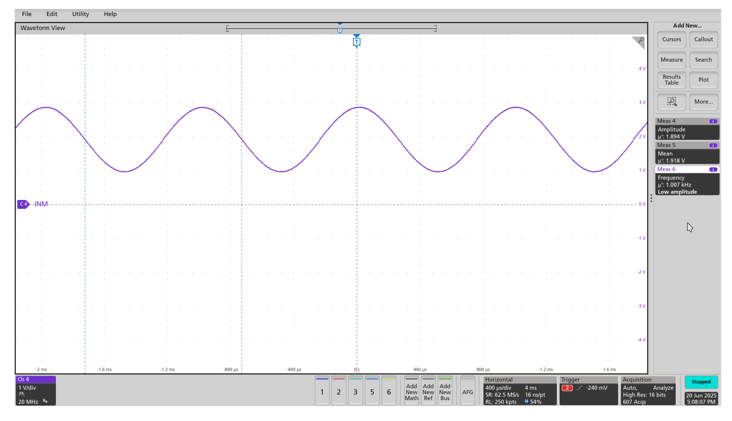
Figure 15.
Half-wave rectified:
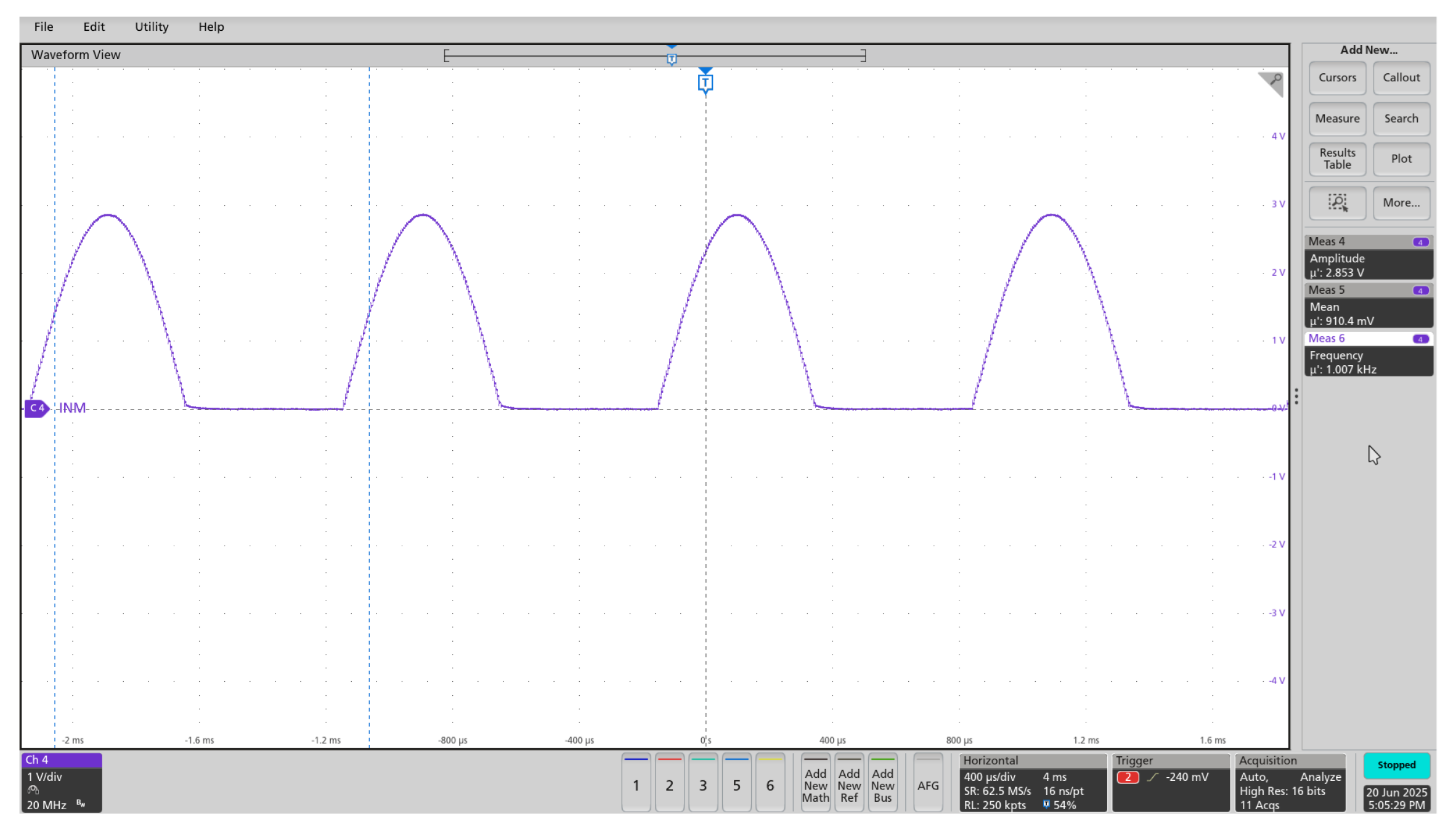
Figure 16.
Full-wave rectified: , inverted
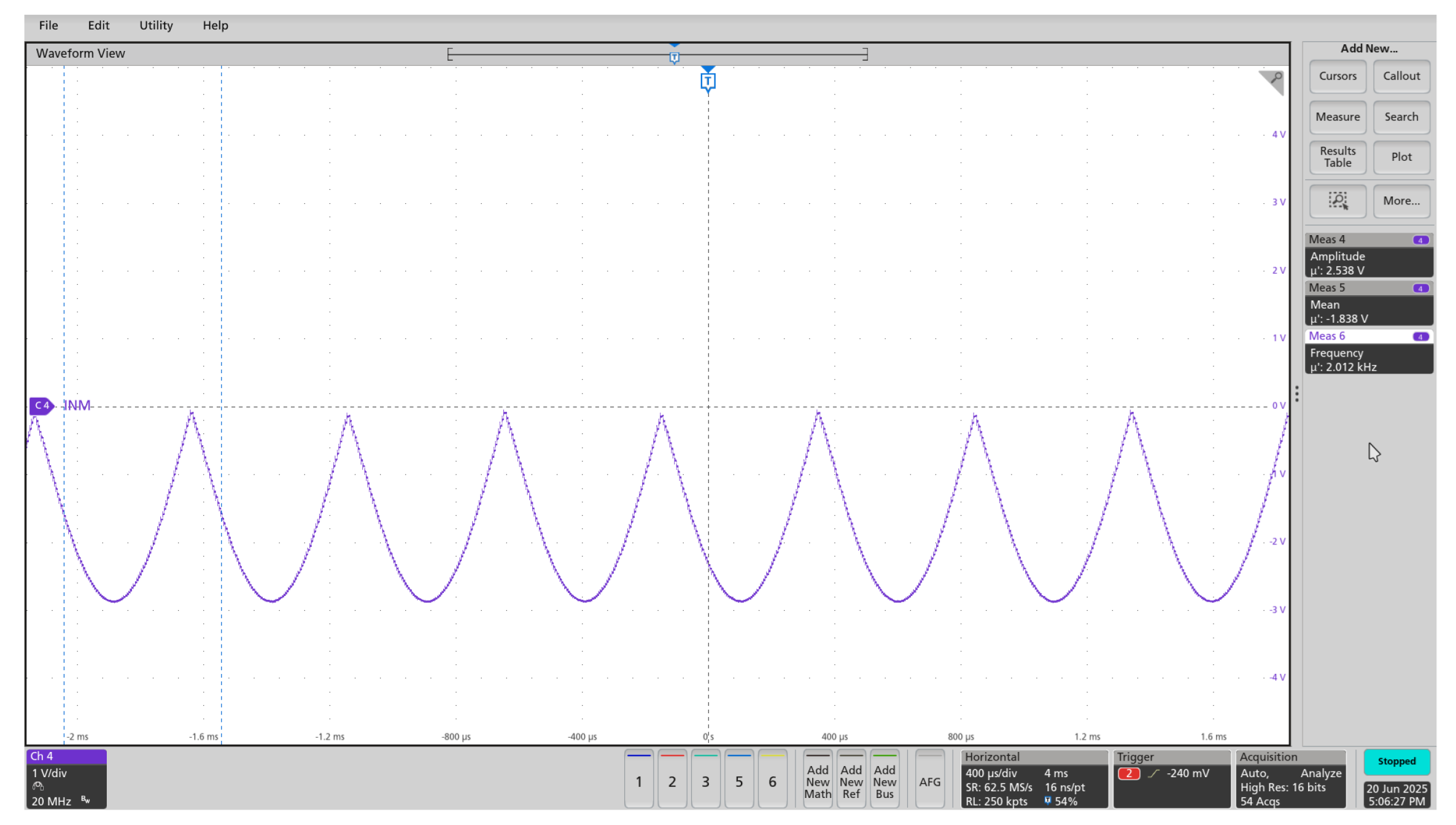

Table 1.
Constant coefficients used in the proposed polynomial approximation of the cosine function.
Table 1.
Constant coefficients used in the proposed polynomial approximation of the cosine function.
| Coefficient | Value |
|---|---|
| 0.999970210689953068626323587055728078 | |
| -0.499782706704688809140466617726333455 | |
| 0.0413661149638482252569383872576459943 | |
| -0.0012412397582398600702129604944720102 |
Table 2.
Firmware functions used for system control
| Functions |
|---|
| dec_to_bin(value, sign, no_of_bits_for_int, no_of_bits_for_frac) |
| bin_to_dec(value, sign, no_of_bits_for_int, no_of_bits_for_frac) |
| sine_config(sin_type, amp, off, freq, phase) |
| control_signal(enable, inverted, load_trig) |
| write_reg(reg_name, write_value) |
| read_reg(reg_name) |
| read_sine_output(x_times) |
Table 3.
Utilization report
| LUTs required for different data bus widths | |||
| Implementation | 16 bits | 24 bits | 32 bits |
| Bhaskara | 1443 | 3363 | 6065 |
| CORDIC | 800 | 912 | 1024 |
| Parabolic synthesis | 179 | 406 | 779 |
| Taylor series | 583 | 2359 | 4043 |
| This Work (1 core) | 36 | 56 | 142 |
| This Work (4 cores) | 342 | 424 | 776 |
Table 4.
Timing report
| Highest delays for different data bus widths[ns] | |||
| Implementation | 16 bits | 24 bits | 32 bits |
| Bhaskara | 75.992 | 119.387 | 159.401 |
| Parabolic synthesis | 18.848 | 29.082 | 34.462 |
| Taylor series | 44.858 | 56.88 | 62.469 |
| This Work (1 core) | 8.402 | 10.352 | 12.656 |
| This Work (4 cores) | 8.247 | 9.952 | 11.936 |
Table 5.
Relative Error comparison
| Relative error for different data bus widths[%] | |||
| Implementation | 16 bits | 24 bits | 32 bits |
| Bhaskara | 0.153 | 0.167 | 0.16 |
| CORDIC | 0.025 | 0.021 | 0.021 |
| Parabolic synthesis | 0.017 | 0.003 | 0.003 |
| Taylor series | 0.001 | 0.0003 | 0.0003 |
| This Work (1 core) | 0.0048 | 0.00032 | 0.00019 |
| This Work (4 cores) | 0.0048 | 0.00032 | 0.00019 |
Table 6.
Figure of Merit Comparison
| This Work(1 core) | This Work (4 cores) | Taylor Series | Parabolic Synthesis | CORDIC | Bhaskara | |
|---|---|---|---|---|---|---|
| 16 bits | 5.807 | 13.538 | 26.152 | 57.354 | 164.940 | 16777.438 |
| 24 bits | 0.742 | 1.350 | 40.254 | 35.422 | 190.601 | 67050.246 |
| 32 bits | 1.366 | 1.760 | 75.769 | 80.538 | 256.672 | 154682.730 |
Disclaimer/Publisher’s Note: The statements, opinions and data contained in all publications are solely those of the individual author(s) and contributor(s) and not of MDPI and/or the editor(s). MDPI and/or the editor(s) disclaim responsibility for any injury to people or property resulting from any ideas, methods, instructions or products referred to in the content. |
© 2026 by the authors. Licensee MDPI, Basel, Switzerland. This article is an open access article distributed under the terms and conditions of the Creative Commons Attribution (CC BY) license.
Copyright: This open access article is published under a Creative Commons CC BY 4.0 license, which permit the free download, distribution, and reuse, provided that the author and preprint are cited in any reuse.


