Submitted:
04 February 2026
Posted:
05 February 2026
You are already at the latest version
Abstract
This review analyzes the transition from silicon to wide-bandgap (WBG) and ultrawide-bandgap (UWBG) semiconductor materials for power electronics, focusing on Silicon Carbide (SiC) and Gallium Nitride (GaN) technologies. Following a PRISMA-based systematic review methodology, we analyzed more than 50 peer-reviewed publications spanning device technology, converter architectures, and system applications. We employ a bottom-up approach, progressing from fundamental material properties through device architectures and converter topologies to system-level implications. We examine how intrinsic material properties enable operation at elevated temperatures, voltages, and frequencies while minimizing losses. Through analysis of Figures of Merit and system-level Key Performance Indicators, we quantify WBG benefits across automotive, industrial, renewable energy, and consumer electronics sectors, demonstrating 3--5x power density improvements and 20--40\% cost reductions. The review presents emerging device technologies including vertical GaN for medium-voltage applications and monolithic bidirectional switches (BDS) enabling single-stage power conversion. We provide the first comprehensive topology-level comparison of emerging vertical GaN and monolithic bidirectional switches against established SiC solutions, identifying specific applications where each technology offers advantages. A comprehensive topology-by-topology comparison between SiC and GaN is provided, offering design guidelines for device selection. The review addresses practical constraints including dynamic on-resistance degradation, threshold voltage instability, and electromagnetic interference challenges for both SiC and GaN. Finally, we examine emerging UWBG materials (Beta-Ga2O3, AlN, c-BN, Diamond) and their development status, manufacturing challenges, supply chain considerations, and commercialization prospects for ultra-high-voltage applications.
Keywords:
efficiency
; gallium nitride (GaN)
; power density
; silicon carbide (SiC)
; wide-bandgap (WBG)
; ultrawide-bandgap (UWBG)
; power electronics
; electric vehicles
; EMI mitigation
; vertical GaN
; bidirectional switch (BDS)
; systematic review
; PRISMA methodology
1. Introduction
The global power electronics sector is experiencing a transformative shift driven by increasingly stringent demands for sustainable energy systems, improved operational efficiency, and reduced carbon emissions. In 2024, energy-related carbon dioxide (CO2) emissions reached approximately Gt, representing an increase of roughly 0.9% compared to 2023 [1]. Although the adoption of clean energy technologies—including solar photovoltaics, wind power, and electric vehicles—has tempered the rate of emissions growth, these persistently high emission levels underscore that incremental improvements alone are insufficient; substantial efficiency gains across the entire energy conversion chain are essential [2].
The historical trend of global carbon dioxide emissions from energy and industrial sources (1970–2024), highlighting the urgency of reducing emissions growth through more efficient power conversion technologies is shown in Figure 1. Based on these charts, global CO2 emissions have more than doubled from 15.0 GtCO2/year in 1970 to 36.3 GtCO2/year in 2024, showing a steady upward trend over five decades. The only notable interruption was a temporary decrease down to 33.3 GtCO2/year in 2020, likely due to pandemic-related economic slowdowns, followed by a rapid rebound in subsequent years.
Central to addressing this challenge is the transition from traditional silicon-based power semiconductors to wide-bandgap (WBG) and ultrawide-bandgap (UWBG) materials, most notably Silicon Carbide (SiC) and Gallium Nitride (GaN) [3,4]. This technological evolution represents far more than a simple material substitution; it constitutes a paradigm shift in power conversion capability that enables revolutionary improvements in efficiency, power density, and thermal performance across virtually all application domains [5,6,7].
The cascading benefits of improved power electronics efficiency across different application sectors demonstrate how WBG technology contributes to overall system sustainability through environmental, economic, and technical improvements. These factors are summed up in Figure 2, where a 2-5% efficiency improvement in WBG devices translates into reduced carbon footprints and lower energy waste environmentally, reduced electricity costs and lower cooling requirements economically, and higher power density with increased switching frequency technically.
Power converters based on semiconductor switching devices regulate energy flow in nearly every modern electrical system, from renewable energy installations and electric vehicle drivetrains to industrial motor drives and data center infrastructure. Even modest improvements in converter efficiency—on the order of 2–5%—can yield substantial reductions in overall energy consumption and associated emissions when deployed at scale [8,9]. The cascading benefits of WBG technology extend beyond raw efficiency improvements to encompass reduced cooling requirements, smaller passive components, and enhanced system reliability.
The economic case for WBG adoption is equally compelling. In large-scale facilities such as data centers operating 10 MW of server power supplies, improving efficiency from 94% to 98% through advanced GaN and SiC power supply units can result in annual energy savings exceeding $700k while simultaneously reducing cooling requirements by nearly halving power delivery network losses from 17% to approximately 9% [10]. For electric vehicles, a 5–10% efficiency improvement from SiC-based 800V traction inverters translates to approximately 7% additional driving range without increasing battery capacity, directly enhancing user experience while reducing battery degradation and total cost of ownership [11,12].
This review paper provides a comprehensive analysis of the current state and future prospects of WBG and UWBG power semiconductors using a bottom-up approach. Section 2 presents fundamental material properties and comparative analysis through various figures of merit. Section 3 provides an in-depth analysis of emerging UWBG materials including their development status and commercialization timeline. Section 4 analyzes SiC and GaN device configurations. Section 5 addresses converter topologies for both SiC and GaN devices. Section 6 provides a comprehensive SiC vs. GaN comparison including gate driver requirements. Section 7 presents system-level dynamic validation through Double Pulse Test simulations comparing GaN and SiC switching behavior. Section 8 discusses system-level implications and quantifies benefits across multiple performance dimensions. Section 9 examines the application landscape with detailed case studies. Section 10 covers reliability considerations and practical constraints for both SiC and GaN technologies. Finally, Section 11 provides conclusions and future research directions. The list of acronyms is provided at the end of the document.
1.1. Literature Review Methodology
This review follows a systematic approach adapted from the PRISMA (Preferred Reporting Items for Systematic Reviews and Meta-Analyses) guidelines to ensure transparency, reproducibility, and comprehensiveness in the literature selection process [13].
1.1.1. Search Strategy and Databases
The literature search was conducted across multiple academic databases including IEEE Xplore, ScienceDirect, Web of Science, Scopus, and Google Scholar. The search period covered publications from January 2014 to December 2025, capturing the critical decade of WBG commercialization and maturation. The primary search keywords and Boolean combinations employed were:
- Primary keywords: “wide bandgap semiconductors”, “silicon carbide power devices”, “gallium nitride HEMT”, “SiC MOSFET”, “GaN power electronics”
- Secondary keywords: “ultrawide bandgap”, “power converter topology”, “electric vehicle inverter”, “DC-DC converter”, “gate driver design”
- Emerging technology keywords: “vertical GaN”, “bidirectional switch”, “gallium oxide power”, “diamond semiconductor”, “aluminum nitride”
- Application keywords: “traction inverter”, “on-board charger”, “solar inverter”, “data center power supply”
Boolean combinations such as (“SiC” OR “GaN”) AND (“power converter” OR “inverter” OR “DC-DC”) AND (“efficiency” OR “power density” OR “switching frequency”) were employed to capture the intersection of device technology and converter applications.
1.1.2. Screening and Selection Process
Figure 3 presents the PRISMA flow diagram illustrating the systematic literature selection process.
Table 1 summarizes the distribution of selected literature by category.
1.1.3. Inclusion and Exclusion Criteria
Studies were included if they: (1) presented original research or comprehensive reviews on WBG/UWBG power semiconductor devices; (2) provided quantitative data on device performance, converter efficiency, or system-level benefits; (3) were published in peer-reviewed journals or major IEEE conference proceedings; (4) addressed practical implementation aspects including reliability, EMI, or thermal management.
Studies were excluded if they: (1) focused exclusively on RF/microwave applications without power electronics relevance; (2) presented only simulation results without experimental validation; (3) were superseded by more comprehensive studies from the same research group; (4) lacked quantitative performance metrics for comparison.
1.2. Comparison with Existing Review Literature and Added Value
Table 2 presents a systematic comparison between this review and recent similar publications, highlighting the unique contributions and gaps addressed by this work. While existing reviews focus on specific aspects such as industrial device reliability, material properties, thermal management, or sustainability perspectives, this 2026 review uniquely provides a comprehensive system-level analysis of both WBG and UWBG technologies. Our work addresses the limitations of prior works by incorporating emerging device coverage (vertical GaN and monolithic BDS), detailed converter topology comparisons, quantitative economic analysis, and up-to-date commercial landscapes through 2025.
Beyond the comprehensive reviews compared in Table 2, several specialized reviews provide valuable insights into specific technical domains. In thermal management, Belguith et al. [19] present advanced cooling techniques for high-power-density GaN converters, while Qin et al. [20] and Zhou et al. [21] address device-level thermal management and packaging challenges for WBG and UWBG devices. For electromagnetic compatibility, Zhang and Wang [22] provide a comprehensive EMI survey addressing the challenges introduced by fast WBG switching transients. In the UWBG domain, Donato et al. [23] present the state of the art for diamond power devices, while Green et al. [24] examine -Ga2O3 power electronics specifically. For reliability, Akbar et al. [25] focus on SiC MOSFET failure modes, complementing the broader reliability coverage in this review. Additionally, Adeloye et al. [26] provide a recent comparative review of GaN in electric vehicle systems. The work by Wu et al. [27] was considered as not concurrent in this review and it was included as a reference in Section 6.5.2.
1.2.1. Unique Contributions and Added Value
This review addresses several critical gaps in the existing literature:
(1) Comprehensive Topology-by-Topology SiC vs. GaN Comparison: Unlike previous reviews that focus primarily on device-level characteristics, this work provides detailed design guidelines for device selection across all major converter topologies (Table 9), enabling practicing engineers to make informed technology choices based on specific application requirements. While She et al. [17] and Musumeci & Barba [18] address converter applications, neither provides systematic topology-level selection criteria spanning both SiC and GaN with quantitative metrics.
(2) Emerging Device Technologies: This review provides the first comprehensive coverage of vertical GaN power devices and monolithic bidirectional switches (BDS) in the context of converter topologies. While Buffolo et al. [8] acknowledge these technologies, our work provides detailed analysis of their impact on specific topologies including matrix converters, Vienna rectifiers, and current-source inverters—analysis absent from all prior reviews.
(3) Updated UWBG Materials Assessment: The UWBG section (Section 3) incorporates the latest developments through 2025. Previous reviews [3,16] lack these recent milestones, and even the 2023 UWBG coverage in Rafin et al. [14] does not capture these 2024–2025 advances.
(4) Bottom-Up Systematic Approach: This review uniquely employs a bottom-up methodology (Materials → Devices → Converters → Systems), providing clear traceability from fundamental material properties through figures of merit to system-level KPIs. This approach enables readers to understand why specific devices excel in particular applications—a framework absent from prior works that typically separate device physics from application discussions.
(5) Quantitative System-Level Benefits:Section 8 provides quantified economic analysis with payback periods for each application sector (Table 14)—data largely absent from device-focused reviews. While Chow et al. [15] discuss system-level sustainability, they do not provide the sector-specific economic quantification presented here.
(6) Practical Design Constraints: The review addresses real-world implementation challenges including dynamic degradation mechanisms, threshold voltage instability, and gate driver optimization requirements (Table 11) that are often overlooked in material-focused surveys. Although Akbar et al. [25] address SiC reliability and Musumeci & Barba [18] discuss GaN challenges, neither integrates these constraints with topology-specific design guidelines as presented here.
Table 3 demonstrates that this review uniquely bridges the gap between device-centric technical analyses and application-level discussions through three key dimensions. The New Data contributions (vGaN/BDS coverage, 2025 UWBG updates) address the temporal lag in existing reviews, while the New Framework (bottom-up methodology, PRISMA compliance) provides transparent systematic analysis absent in prior work. Most critically, the New Insights deliver actionable quantitative guidance—topology-specific device selection criteria and economic payback analysis—that enable engineers to translate theoretical WBG advantages into practical deployment decisions across automotive, industrial, and renewable energy applications.
1.2.2. Research Gap Analysis
Figure 4 illustrates the positioning of this review relative to existing literature across two key dimensions: device technology depth and system integration scope. This review uniquely spans from fundamental device technology through system-level integration while incorporating emerging UWBG technologies, distinguishing itself from prior works that either focused narrowly on device/material aspects [8,16,23] or emphasized system-level applications without comprehensive device coverage [14,15].
The landscape of WBG review literature reveals three distinct clusters: (i) device-focused reviews that provide deep technical analysis but limited application guidance [8,16,25]; (ii) material-focused reviews covering emerging UWBG semiconductors but lacking converter-level analysis [3,23,24]; and (iii) application-focused reviews addressing specific sectors but without systematic device comparison [18,26]. This review bridges these clusters through its bottom-up methodology and comprehensive scope.
2. Material Properties and Comparative Analysis
The fundamental material properties of semiconductors determine the ultimate performance limits achievable in power electronic devices. WBG and UWBG materials demonstrate exceptional versatility across power electronics and Radio Frequency (RF) applications due to their capacity to operate reliably in high-temperature and harsh environments [4,16].
2.1. Intrinsic Material Characteristics
Table 4 summarizes the key properties of silicon alongside WBG materials (4H-SiC, GaN) and emerging UWBG materials (-Ga2O3, AlN, c-BN, Diamond). The UWBG materials exhibit significantly superior properties compared to silicon, with bandgaps ranging from 4.9 to 6.4 eV and breakdown fields of 8–15 MV/cm, though trade-offs exist in electron mobility and thermal conductivity, where diamond leads with 23 W/cmK and GaN achieves the highest mobility at 2000 cm2/Vs.
Figure 5 provides a comprehensive radar chart comparison between silicon and U/WBG devices across multiple key parameters, visually demonstrating the performance advantages of advanced semiconductor materials. Diamond and c-BN exhibit exceptional thermal conductivity and maximum temperature capabilities, while GaN achieves superior switching speed and maximum frequency, and SiC offers a balanced profile with strong performance across on-resistance, power density, and thermal management, clearly outperforming silicon in all metrics.
The bandgap energy represents the energy required to excite an electron from the valence band to the conduction band. Materials with larger bandgaps exhibit higher intrinsic breakdown voltages and can operate at elevated temperatures without excessive thermally-generated leakage current [5]. The wide bandgap of SiC (3.23 eV) and GaN (3.4 eV) compared to silicon (1.12 eV) fundamentally enables operation at higher voltages and temperatures.
The critical electric field defines the maximum electric field a material can sustain before avalanche breakdown occurs [17]. SiC and GaN exhibit critical fields approximately 8–11× higher than silicon, while UWBG materials such as -Ga2O3 and AlN approach 30–50× improvement.
Electron mobility quantifies how rapidly charge carriers drift through the material under an applied electric field [28]. While SiC exhibits somewhat lower mobility than silicon (950 vs. 1440 cm2/Vs), GaN offers superior mobility (2000 cm2/Vs), and diamond presents exceptional mobility (4500 cm2/Vs) for future applications.
Thermal conductivity governs the ability to conduct heat away from active device regions, critically impacting power handling capability and long-term reliability [29]. SiC’s thermal conductivity ( W/cm · K) substantially exceeds that of silicon ( W/cm · K), while diamond’s exceptional value ( 23 W/cm · K) positions it as the ultimate material for extreme power density applications.
2.2. Quantitative Performance Metrics: Figures of Merit
Several Figures of Merit (FOMs) have been developed to enable quantitative comparison of semiconductor technologies [30,31,32,33].
Baliga’s Figure of Merit (BFOM) characterizes the trade-off between on-resistance and breakdown voltage for unipolar power devices [30]:
Baliga High-Frequency Figure of Merit (BHFFOM) accounts for switching losses [34]:
Johnson’s Figure of Merit (JFOM) characterizes the maximum power-frequency product [31]:
Keyes’ Figure of Merit (KFOM) evaluates thermal management and power density limits [32]:
Combined High-Frequency Figure of Merit (CHFFOM) extends BHFFOM to include thermal effects [33]:
Thermal Figure of Merit (TFOM) [19] specifically addresses heat dissipation capability:
where is Boltzmann’s constant and T is absolute temperature.
Table 5 presents normalized FOM values relative to silicon. Diamond demonstrates the highest performance across all FOMs with BFOM of 50000× and CHFFOM of 2114× relative to silicon, while -Ga2O3 excels in BFOM (3444×) but shows lower performance in frequency-related metrics, and GaN offers a balanced profile with strong BFOM (846×) and competitive performance across switching and thermal FOMs.
3. Emerging UWBG Materials: Development Status and Commercialization
While SiC and GaN technologies have achieved commercial maturity, ultrawide-bandgap (UWBG) materials represent the next frontier in power semiconductor development. These materials, characterized by bandgaps exceeding 4 eV, offer theoretical performance advantages that could enable applications beyond the capabilities of current WBG devices [3].
3.1. Beta-Gallium Oxide (-Ga2O3)
-Ga2O3 has emerged as one of the most promising UWBG materials due to its unique combination of properties and manufacturing advantages [24]. With a bandgap of 4.9 eV and a critical electric field of 8 MV/cm, -Ga2O3 exhibits a Baliga Figure of Merit (BFOM) more than 3000× that of silicon, suggesting tremendous potential for high-voltage power devices.
A key advantage of -Ga2O3 is its compatibility with melt-growth techniques including the Floating Zone (FZ), Czochralski (CZ), and Edge-defined Film-fed Growth (EFG) methods. These methods enable production of large-diameter, high-quality single-crystal substrates at potentially lower costs than the vapor-phase growth required for SiC and GaN substrates. Currently, 2-inch substrates are commercially available from multiple suppliers, with 4-inch substrates in limited commercial production and 6-inch substrates demonstrated in research laboratories [35]. While substrate manufacturing has reached commercial maturity, device technology remains at the validation stage (TRL 5–6 per Horizon 2020 definitions), reflecting the gap between substrate availability and device qualification for end-use applications.
However, -Ga2O3 faces two fundamental challenges. First, its relatively low thermal conductivity (0.1–0.3 W/cmK) is approximately 10–30× lower than SiC, necessitating sophisticated thermal management solutions including heterogeneous integration with high-thermal-conductivity substrates. Second, the absence of effective p-type doping limits device architectures to unipolar configurations such as Schottky Barrier Diodes (SBDs) and Field-Effect Transistors (FETs). Recent research has explored heterostructures with NiOx and other p-type materials to enable bipolar operation [36].
The global market for high-purity -Ga2O3 power devices is projected to grow at a Compound Annual Growth Rate (CAGR) of approximately 24.5% from 2024 to 2033, with applications initially targeting the 600 V–3.3 kV range for EV power systems, solar inverters, and grid interface equipment.
3.2. Aluminum Nitride (AlN)
Aluminum nitride possesses the highest critical electric field (15 MV/cm) among practical UWBG semiconductors, enabling exceptionally thin drift regions and low on-resistance for a given breakdown voltage [37]. Its bandgap of 6.2 eV and Johnson’s Figure of Merit 5× higher than GaN make it particularly attractive for both high-power switching and high-frequency applications.
A major breakthrough was reported at the IEEE International Electron Devices Meeting (IEDM) in December 2023, where researchers from Nagoya University demonstrated AlN-based diodes capable of withstanding electric fields of 7.3 MV/cm—approximately twice the capability of SiC or GaN [37]. This achievement utilized the Distributed Polarization Doping (DPD) technique, which enables effective n-type and p-type doping in AlGaN alloys without conventional impurity dopants, circumventing AlN’s historically problematic doping challenges.
In 2024, a German research consortium led by Fraunhofer IISB successfully demonstrated a complete value chain for AlN-based devices in Europe [37]. The consortium grew AlN crystals up to 43 mm diameter, processed them into polished wafers, and fabricated AlN/GaN high-electron-mobility transistors (HEMTs) with breakdown voltages up to 2200 V and power densities superior to both SiC and GaN devices. These AlN/GaN HEMTs offer up to 3000× lower conduction losses than silicon and are approximately 10× more efficient than SiC transistors.
Crystal IS has achieved production of 100 mm (4-inch) diameter single-crystal AlN substrates with 99% usable area, a significant milestone toward commercial viability [37]. Researchers at Nagoya University project commercialization of AlN-based power devices in the 2030s, contingent on resolving remaining challenges in ohmic contact formation and scaling manufacturing processes.
3.3. Diamond
Diamond represents the ultimate semiconductor material, offering an unparalleled combination of an ultra-wide bandgap (5.5 eV), the highest thermal conductivity of any material (22–23 W/cmK), exceptional carrier mobility (4500 cm2/Vs for electrons, 3800 cm2/Vs for holes), and a theoretical critical electric field of 10–20 MV/cm [23]. These properties yield a BFOM 50,000× that of silicon, positioning diamond as the long-term solution for extreme power density applications.
Significant progress has been made in diamond device development. Researchers at the University of Illinois Urbana-Champaign demonstrated diamond Schottky barrier diodes with the highest reported breakdown voltage (4.6 kV at 0.01 mA/mm) and lowest leakage current among diamond devices [23]. Japan’s National Institute for Materials Science (NIMS) achieved another milestone in 2024 with the world’s first n-channel diamond MOSFET, exhibiting field-effect mobility over 150 cm2/Vs at 573 K—the highest among all n-channel MOSFETs based on wide-bandgap semiconductors [23].
Japanese institutions are leading diamond semiconductor commercialization efforts. Saga University developed the world’s first diamond-based power device in 2023 in collaboration with the Japan Aerospace Exploration Agency (JAXA) for high-frequency space communication applications. Orbray has developed mass-production technology for 2-inch diamond wafers and is progressing toward 4-inch substrates, with partnerships including Toyota and Denso supporting onboard power device development expected in the 2030s [23].
Diamond’s primary challenges include the difficulty of n-type doping due to high activation energies, the lack of a mature manufacturing ecosystem, and substrate availability limitations. However, advances in chemical vapor deposition (CVD) growth and recent n-channel MOSFET demonstrations suggest these barriers are being systematically addressed.
3.4. Cubic Boron Nitride (c-BN)
Cubic boron nitride represents a compelling UWBG semiconductor that combines many of diamond’s exceptional properties with potentially superior doping characteristics [38,39]. With a bandgap of 6.4 eV—the highest among practical semiconductors—and a theoretical critical electric field of 12 MV/cm, c-BN offers extraordinary high-voltage capability. Its thermal conductivity of 13 W/cmK, while lower than diamond, significantly exceeds that of SiC and GaN.
The key advantage of c-BN over diamond lies in its doping flexibility. Both n-type and p-type doping have been demonstrated with activation energies lower than those in diamond, potentially enabling efficient bipolar devices [38]. Silicon substituting on the boron site (SiB) serves as an effective n-type dopant, while beryllium and magnesium provide p-type conductivity. Recent work at North Carolina State University demonstrated n-type conductivity with carbon doping concentrations ranging from to , achieving semiconductor-like resistivity profiles [40].
Manufacturing c-BN remains challenging. Conventional High-Pressure, High-Temperature (HPHT) synthesis at >1,150°C and >2.5 GPa produces only millimeter-scale crystals—far below the centimeter-scale wafers required for electronics manufacturing [39]. However, breakthrough fabrication techniques are emerging:
Pulsed Laser Annealing (PLA): Researchers have demonstrated direct conversion of hexagonal BN (h-BN) into phase-pure single-crystal c-BN using nanosecond laser pulses, achieving conversion in approximately 200 ns at ambient pressure [41]. This technique can produce epitaxial c-BN thin films on sapphire substrates with controlled doping.
Solution growth: Texas Tech University, with Department of Energy (DOE) funding, is developing autoclave-based solution growth methods that could enable scalable production of electronic-grade c-BN wafers for extreme-temperature electronics [38].
Diamond/c-BN heterostructures: First-principles calculations indicate that diamond/c-BN heterojunctions can form high-density two-dimensional carrier gases at the interface, potentially enabling high-frequency, high-power devices that leverage both materials’ advantages [42].
The projected applications for c-BN power devices include ultra-high-voltage (>10 kV) grid infrastructure, extreme-environment electronics for aerospace and geothermal applications, and next-generation smart grid transformers. While commercialization remains in the ≥2035 timeframe, c-BN’s combination of UWBG properties and doping flexibility positions it as a potential ultimate solution for extreme power electronics.
4. WBG Device Architectures: SiC and GaN
The commercial landscape of WBG semiconductors has matured significantly [43,44]. This section presents device configurations for both SiC and GaN technologies.
4.1. SiC Device Configurations
Silicon Carbide power devices have evolved into several mature device architectures, each offering distinct advantages for specific application requirements [5,17]. Figure 6 presents the classification of commercial SiC power devices. SiC power devices are categorized into unipolar devices (MOSFETs, JFETs, and SBDs) and bipolar devices (BJTs, thyristors, and IGBTs), with unipolar devices dominating commercial applications due to their superior switching characteristics and reduced reverse recovery losses.
4.1.1. SiC MOSFET Structure
The SiC MOSFET is the dominant commercial device, offering normally-off operation with voltage-controlled switching [45]. The planar MOSFET suffers from the “JFET effect”—the narrow conduction path between adjacent p-wells increases on-resistance. Trench MOSFETs eliminate this limitation by orienting the channel vertically, achieving 30–50% lower specific on-resistance [46]. The on-resistance of a SiC MOSFET can be expressed as:
where is channel resistance, is the JFET region resistance (eliminated in trench designs), is drift region resistance, is substrate resistance, and represents contact resistances. Figure 7 illustrates the planar and trench SiC MOSFET structures. The planar SiC MOSFET features a horizontal channel with gate oxide on the semiconductor surface, while the trench MOSFET incorporates a vertical channel structure with the gate embedded within a trench, enabling higher channel density and lower on-resistance at the cost of increased gate oxide electric field stress.
4.2. SiC Device Selection Criteria and Loss Models
The selection of SiC MOSFETs for power converter applications requires evaluation of key physical parameters and their impact on system performance. The fundamental selection criteria include:
Breakdown Voltage (): SiC devices are commercially available with ratings from 650 V to 1700 V. The drift region resistance scales with blocking voltage as , where is electron mobility, is permittivity, and is critical electric field (2.2–3 MV/cm for SiC).
On-State Resistance (): Total on-resistance comprises channel and drift components: . SiC exhibits positive temperature coefficient above 25°C, enabling natural current sharing in parallel configurations.
Switching Frequency (): SiC MOSFETs typically operate at 20–150 kHz in hard-switching applications. Gate charge and output capacitance determine switching speed capability.
Power Loss Models: Total device losses comprise conduction and switching components:
Switching energy can be estimated analytically from datasheet parameters:
where , , , are current rise, voltage fall, voltage rise, and current fall times, respectively, and is reverse recovery charge.
Gate Drive Requirements: Recommended gate voltage is = +15 to +20 V (on) and −2 to −5 V (off). The Miller plateau voltage determines the voltage fall/rise duration during switching transitions.
Thermal Considerations: Junction-to-case thermal resistance and maximum junction temperature (typically 175–200°C) define power density limits. Thermal impedance is critical for pulsed operation.
4.3. GaN Device Configurations
Figure 8 presents the classification of GaN HEMT devices. GaN power devices are categorized into GaN-on-Si structures using E-Mode and D-Mode HEMTs (with discrete or cascode configurations) and GaN-on-GaN structures utilizing V-GaN FETs, where GaN-on-Si dominates commercial markets due to cost advantages while GaN-on-GaN offers superior performance through reduced substrate-related defects.
Figure 9 illustrates the different types of GaN devices including normally-on and normally-off configurations. The figure shows the evolution from D-Mode (normally-on) GaN HEMTs to E-Mode (normally-off) configurations through various enhancement techniques, including cascode configurations that combine low-voltage Si MOSFETs with high-voltage D-Mode GaN devices to achieve normally-off operation with improved gate drive compatibility.
4.3.1. Depletion-Mode (D-Mode) GaN HEMTs
D-mode devices are inherently normally-on, requiring a negative gate voltage to turn off. The Two-Dimensional Electron Gas (2DEG) at the AlGaN/GaN interface provides exceptionally high electron mobility and carrier density. Figure 10 shows the internal structure of a D-mode GaN HEMT, as described in detail in [47,48].
4.3.2. Enhancement-Mode (E-Mode) GaN HEMTs
4.4. GaN Device Selection Criteria and Loss Models
GaN HEMTs offer distinct advantages for high-frequency power conversion, requiring specific selection criteria:
Breakdown Voltage (): Commercial GaN HEMTs are rated at 100–650 V, with emerging devices reaching 1200 V. The lateral structure and 2DEG channel provide high electron mobility (∼2000 cm2/Vs) enabling low .
On-State Resistance (): GaN exhibits positive temperature coefficient, with , where 1.5–2.0. Dynamic increase due to charge trapping must be considered in loss calculations.
Switching Frequency (): GaN HEMTs enable MHz-range operation (1–10 MHz) due to significantly lower gate charge ( typically 5–15 nC) and output charge () compared to SiC, achieving 10× reduction versus equivalent Si devices.
Power Loss Models: For high-frequency GaN applications, capacitive losses become significant:
where represents output capacitance energy loss.
Conduction losses dominate in GaN converters due to reduced switching losses, for example considering a buck converter:
where D is duty cycle and is body diode (or anti-parallel diode) forward voltage.
Gate Drive Requirements: Enhancement-mode GaN HEMTs require = +5 to +6 V (on) and 0 V (off), with maximum typically limited to 7 V. Negative turn-off voltage (−3 V) is recommended to prevent spurious turn-on from induced gate charging.
Thermal Considerations: GaN-on-Si devices have = 150–175°C. The lateral heat spreading and thermal boundary resistance at the GaN/substrate interface require careful PCB thermal design with thermal vias directly beneath the device.
Power Density: GaN enables power densities exceeding 100 W/in3 due to reduced passive component size at high frequencies, with inductor volume scaling approximately as [5].
4.5. Vertical GaN Power Devices
While lateral GaN HEMTs dominate the commercial market for voltages up to 650 V, vertical GaN devices are emerging as critical enablers for medium-voltage applications (1.2–10 kV) where they compete directly with SiC [51]. Unlike lateral devices where voltage scaling requires proportionally larger chip area, vertical GaN conducts current perpendicular to the substrate surface, allowing breakdown voltage to increase through drift layer thickness while maintaining compact chip dimensions.
Recent advances have demonstrated impressive performance milestones. Vertical GaN (vGaN) technology features 1,200 V-class devices capable of reducing system losses by nearly 50% compared to lateral GaN, while achieving approximately 3× smaller die size [51]. Vertical GaN transistors with operating currents exceeding 50 A have been demonstrated, enabling MHz-frequency operation in compact packages [51].
Vertical GaN architectures include trench MOSFETs (T-MOSFETs), Current Aperture Vertical Electron Transistors (CAVETs), and vertical Junction Field-Effect Transistors (JFETs). The 1.2 kV vertical GaN fin-channel JFET has emerged as a particularly promising device, offering normally-off operation, avalanche capability, and no dynamic degradation—addressing one of the primary reliability concerns of lateral GaN HEMTs [52].
Key challenges for vertical GaN include the limited availability of native GaN substrates (currently 2–4 inch), high substrate costs, and the difficulty of achieving low background doping ( ) in thick drift layers required for 1.2 kV+ operation. However, advances in GaN-on-engineered-substrate technology are enabling 200 mm CMOS-compatible fabrication pathways that could dramatically reduce costs [53].
4.6. GaN Bidirectional Switches (BDS)
Monolithic bidirectional switches represent a paradigm shift in power semiconductor technology, enabling four-quadrant operation—bidirectional current flow and bipolar voltage blocking—from a single device [43]. While conventional approaches require four discrete transistors in back-to-back configurations (doubling and component count), GaN BDS devices leverage the lateral HEMT structure to integrate two opposing gates sharing a common drift region. An example is provided in the following Section 5.1.2.
Commercial GaN BDS devices offer ratings at 40 V, 650 V, and 850 V with four operational modes: full conduction, full blocking, and two diode modes (forward and reverse blocking) [43].
Key applications for GaN BDS include matrix converters (direct AC-AC conversion without DC-link), Vienna rectifiers (three-level PFC with bidirectional current capability), T-type inverters (three-level topologies for solar and motor drive applications), Current-Source Inverters (CSI) for high-power motor drives and High-Voltage Direct Current (HVDC) transmission, and Highly Efficient and Reliable Inverter Concept (HERIC) inverters for Photovoltaic (PV) applications with reactive power capability.
Table 7 summarizes the key differences between WBG device technologies. GaN HEMTs offer the best switching speed (1–40 MHz) and minimal reverse recovery losses with low on-resistance (1–5 mcm2), while SiC MOSFETs provide superior high-voltage capability (650–3300 V) and higher current ratings (5–200 A), and Si IGBTs remain cost-effective for high-power applications despite significantly slower switching speeds (0.02–0.1 MHz) and poor reverse recovery characteristics.
5. Converter Topologies for WBG Devices
5.1. SiC Converter Topologies
SiC devices excel in high-power, high-voltage converter applications where their superior breakdown voltage and thermal conductivity provide significant advantages over both Si and GaN alternatives [17].
5.1.1. Three-Phase Traction Inverter
The three-phase voltage source inverter is the dominant topology for electric vehicle traction drives [54]. Figure 12 shows a SiC-based traction inverter configuration. The three-phase voltage source inverter (VSI) topology consists of six SiC MOSFETs (–) arranged in three half-bridge legs with a DC-link capacitor (), enabling bidirectional power flow and efficient motor control for electric vehicle traction applications.
The power loss in each SiC MOSFET comprises conduction and switching components:
SiC enables switching frequencies of 10–20 kHz in traction applications (versus 5–10 kHz for Si IGBTs), reducing motor current ripple and acoustic noise while maintaining >98% inverter efficiency [12].
5.1.2. DC Fast Charging Converter
DC fast charging stations (50–350 kW) leverage SiC’s high-voltage capability and efficiency [56]. Figure 13 shows a typical three-phase Vienna rectifier front-end with isolated DC-DC stage. The topology combines a three-phase Vienna rectifier for AC/DC conversion with bidirectional switches and diodes for power factor correction, followed by isolated DC/DC converter stages that provide galvanic isolation and voltage regulation for EV battery charging applications.
The Vienna rectifier achieves near-unity power factor with reduced switch count compared to conventional Pulse Width Modulation (PWM) rectifiers, while SiC enables operation at 30–50 kHz for compact magnetic design.
5.1.3. Grid-Tied Solar Inverter
Central and string inverters for photovoltaic applications benefit from SiC’s efficiency at partial load conditions [57]. Figure 14 shows a three-level T-type inverter topology. The configuration features a DC-link with split capacitors and bidirectional switches in each phase leg, enabling three-level voltage output that reduces harmonic distortion and improves efficiency for grid-tied solar PV applications through reduced stress and lower filtering requirements.
Three-level topologies reduce the voltage stress on each device to , enabling higher DC-link voltages (up to 1500 V for utility-scale installations) while maintaining acceptable levels. The output voltage Total Harmonic Distortion (THD) is significantly improved:
5.2. GaN Converter Topologies
Implementing GaN devices in power converter topologies requires careful consideration of their unique characteristics [58,59]. Printed Circuit Board (PCB) layout is critical for achieving optimal performance.
5.2.1. Buck Converters
The synchronous buck converter represents an ideal topology for demonstrating GaN advantages [18]. The inductance value is selected to maintain Continuous Conduction Mode (CCM) operation [60]:
Output voltage ripple is given by:
5.2.2. Interleaved Buck Converters
5.2.3. Dual Active Bridge Converters
The DAB converter has emerged as a leading topology for bidirectional isolated DC-DC conversion [62,63,64]. Zero Voltage Switching (ZVS) operation is achievable over a wide load range. The average power transfer is [65]:
The inductor current evolution is:
5.2.4. Multilevel DAB Topologies
For medium-voltage applications (>1 kV), multilevel DAB topologies extend capabilities [16]. The three-level Neutral Point Clamped (NPC) DAB reduces voltage stress on individual switches:
5.3. GaN Technology Evolution: Vertical GaN and BDS for Converter Topologies
While the preceding sections focused on established SiC and lateral GaN technologies, this section examines how emerging GaN device architectures—specifically vertical GaN and monolithic bidirectional switches (BDS)—are reshaping converter design possibilities. Table 8 provides a topology-by-topology analysis of how these emerging technologies compare to established SiC solutions. Vertical GaN devices promise 50–100 kHz operation with reduced losses for traction inverters and enhanced switching speed for T-type inverters, while GaN BDS technology offers transformative advantages including single-device solutions for Vienna rectifiers and DAB converters, MHz operation for HERIC inverters, native bidirectional blocking for motor drives, and elimination of DC-link capacitors in single-stage OBC designs, with commercial availability expected between 2025–2029.
5.3.1. Vertical GaN: Challenging SiC in Medium-Voltage Applications
Vertical GaN power devices represent a paradigm shift from traditional lateral GaN-on-Si HEMTs, enabling operation at 1.2 kV and beyond—voltage classes currently dominated by SiC [51,53]. Unlike lateral devices where breakdown voltage scales with chip area, vertical GaN conducts current perpendicular to the substrate, allowing voltage scaling through drift layer thickness while maintaining compact die dimensions.
Topology Implications:
Three-Phase Traction Inverters: The traditional domain of SiC MOSFETs, traction inverters are a prime target for vertical GaN. Onsemi’s 1,200 V vGaN technology demonstrates nearly 50% lower losses compared to lateral GaN and approximately 3× smaller die size [52]. The superior switching figure of merit () enables switching frequencies of 50–100 kHz while maintaining efficiency above 99%, compared to 10–20 kHz typical for SiC traction inverters. The reduced also simplifies soft-switching in resonant topologies.
DC Fast Charging (Vienna Rectifier and DAB): For 800 V battery systems, 1.2 kV vertical GaN enables single-device implementations without series stacking. The absence of dynamic degradation—a key reliability concern in lateral GaN HEMTs [66]—makes vertical GaN particularly attractive for high duty-cycle applications like DC fast chargers.
Grid-Tied Inverters: Medium-voltage applications (1500 V DC-link for utility-scale PV) require 3.3 kV device ratings. Vertical GaN development is progressing toward this voltage class, with 2.3 kV demonstrations reported in research [53]. When commercially available, vertical GaN could challenge SiC in this application through superior switching speed.
Key Advantages over Lateral GaN:
- Voltage scaling through drift layer thickness rather than lateral area
- No dynamic degradation (no surface traps)
- Avalanche capability similar to SiC MOSFETs
- Reduced chip area for given voltage/current rating
Current Limitations:
- Limited substrate availability (2–4 inch GaN-on-GaN)
- Higher substrate cost compared to SiC or GaN-on-Si
- Manufacturing maturity gap (TRL 4–5 vs. TRL 8–9 for SiC)
- Projected commercialization: 2026–2028 for 1.2 kV class
5.3.2. Bidirectional GaN Switches: Enabling Single-Stage Power Conversion
Monolithic bidirectional switches (BDS) represent perhaps the most transformative GaN innovation for power converter topologies [8,26]. By integrating four-quadrant operation (bidirectional current flow and bipolar voltage blocking) into a single device, GaN BDS enables entirely new converter architectures previously impractical with discrete devices.
Revolutionary Topology Enablement:
Single-Stage AC-DC Conversion: Traditional two-stage converters (PFC + isolated DC-DC) require intermediate DC-link capacitors—often the largest, heaviest, and least reliable components. GaN BDS enables single-stage isolated conversion through cycloconverter and matrix-type topologies, eliminating the DC-link entirely [26]. Benefits include:
- 40–50% size reduction in EV on-board chargers
- Elimination of electrolytic capacitors (improved reliability)
- Inherent bidirectional power flow (V2G capability)
- Higher efficiency through single-stage conversion
Matrix Converters (Direct AC-AC): Matrix converters provide direct frequency conversion without DC-link, but historically required complex discrete switch arrays. Each bidirectional switch position previously needed four discrete transistors in anti-series/anti-parallel configuration, quadrupling component count and on-resistance. A single GaN BDS replaces this four-device array, making matrix converters practical for:
- Variable-frequency motor drives
- Solid-state transformers
- Grid frequency conversion
Vienna Rectifiers and T-Type Inverters: These three-level topologies require bidirectional switches for the neutral-point connection. Replacing back-to-back discrete switches with GaN BDS provides:
- 50% reduction in on-resistance for bidirectional current path
- Simplified gate drive (two isolated channels vs. four)
- Higher switching frequency capability (>100 kHz vs. 30–50 kHz)
- Reduced PCB complexity and parasitic inductance
HERIC Inverters for PV: The HERIC topology uses bidirectional switches to decouple the PV array from the grid during freewheeling periods, reducing common-mode leakage current. GaN BDS enables MHz-frequency operation of HERIC inverters while supporting reactive power compensation for grid support functions.
Current-Source Inverters (CSI): CSI topologies require bidirectional voltage blocking, traditionally achieved with series diodes that increase losses. GaN BDS provides native bidirectional blocking with lower on-resistance, enabling CSI adoption for high-power motor drives with improved efficiency and inherent short-circuit protection [18].
5.3.3. Design Guidelines for Technology Selection
Based on the analysis of current SiC capabilities and emerging GaN technologies, the following guidelines assist designers in technology selection.
SiC remains the preferred choice when voltage requirements exceed 1.2 kV (until vertical GaN matures), when high current capability above 100 A with an established supply chain is required, or when short-circuit withstand capability is critical. Additionally, SiC should be selected for applications demanding junction temperatures exceeding 175°C or where proven reliability and qualification data are mandatory.
Vertical GaN should be considered for designs targeting the 2027+ timeframe when maximum switching frequency above 50 kHz provides meaningful benefits, when power density represents the primary optimization target, or when dynamic stability is critical for continuous hard-switching operation. This technology is also attractive when avalanche capability combined with superior switching FOM is desired, particularly for voltage classes between 650 V and 1.2 kV.
GaN BDS technology is recommended when bidirectional current flow and voltage blocking are required, when single-stage conversion topology is feasible, or when DC-link capacitor elimination offers significant advantages in terms of size, reliability, or cost. This technology is particularly well-suited for Vienna, T-type, HERIC, or matrix topologies, for applications targeting switching frequencies above 100 kHz, and for grid-connected systems requiring reactive power support.
5.3.4. Market and Technology Outlook
The convergence of vertical GaN and BDS technologies is expected to accelerate the displacement of SiC in specific application segments while opening entirely new topology possibilities. Key milestones include:
- 2025: Commercial 650 V GaN BDS devices (Infineon, Navitas); initial vertical GaN sampling at 700–1200 V
- 2026–2027: Production vertical GaN for EV traction; BDS adoption in solar microinverters
- 2028–2030: Vertical GaN challenging SiC in medium-voltage segments; matrix converters becoming mainstream
- 2030+: Potential vertical GaN extension to 3.3 kV for grid applications
The combination of vertical GaN for high-voltage unidirectional applications and BDS for bidirectional topologies positions GaN technology as a comprehensive competitor to SiC across the medium-voltage power electronics landscape, rather than remaining confined to the sub-650 V market segment.
6. SiC vs. GaN: Comprehensive Comparison
6.1. Topology-Specific Comparison
The selection between SiC and GaN devices depends critically on the converter topology, power level, voltage class, and switching frequency requirements. Table 9 provides a comprehensive comparison for the major power converter topologies. SiC devices are recommended for high-power applications (>100 kW two-level VSI, >10 kW buck, >50 kW DAB, >30 kW Vienna rectifiers) due to superior voltage ratings (1.2–3.3 kV) and current handling, while GaN excels in low-to-medium power applications (<1 kW buck, <20 kW DAB, T-type/NPC, LLC resonant) with advantages including 10× lower , MHz switching operation, smaller magnetics, and significantly reduced output capacitance enabling phase current cancellation.
6.2. Thermal Stability Considerations
Table 10 summarizes the key thermal properties governing heat dissipation in wide-bandgap power devices. SiC exhibits superior thermal conductivity (330–490 W/mK), approximately 3× higher than GaN (130–200 W/mK), enabling reliable operation at junction temperatures exceeding 200°C with simplified thermal management. GaN’s thermal conductivity decreases significantly with temperature, creating a thermal management challenge: as device temperature rises under high-power operation, heat dissipation capability diminishes. This self-heating effect reduces carrier mobility, shifts threshold voltage, and approximately doubles failure rates for every 10°C increase in junction temperature, limiting practical GaN operation to 150–175°C. AlN offers thermal conductivity comparable to SiC (285–320 W/mK) combined with a wider bandgap (6.2 eV), making it attractive as a buffer layer or substrate material to improve thermal performance in GaN-based devices.
From a practical standpoint, SiC remains preferred for high-power applications (>10 kW) where thermal conductivity dominates design constraints, enabling smaller heatsinks and simpler cooling solutions. GaN devices require more conservative thermal derating and advanced packaging approaches (double-sided cooling, embedded die) to compensate for lower thermal conductivity. These considerations reinforce the topology-dependent recommendations in Table 9, where SiC is favored for thermally demanding applications (Two-Level VSI >100 kW, Buck >10 kW) while GaN excels in high-frequency, medium-power applications where switching performance advantages outweigh thermal management complexity.
6.3. Efficiency and Loss Comparison
The total losses in a power converter include conduction and switching components. For a given topology, the device selection significantly impacts both:
Conduction losses: SiC MOSFETs exhibit positive temperature coefficient of , improving current sharing in parallel configurations but increasing losses at elevated temperatures. GaN HEMTs have flatter temperature dependence and lower specific on-resistance () below 650 V, but require more devices in parallel for high-current applications.
Switching losses: GaN devices achieve 3–10× lower switching energy () than equivalently-rated SiC MOSFETs due to smaller gate charge and output capacitance. This advantage enables proportionally higher switching frequencies, reducing passive component size according to:
6.4. Application-Specific Recommendations
Based on the comprehensive analysis, the following guidelines emerge:
EV Traction Inverter (>100 kW, 400–800 V): SiC MOSFET is the clear choice due to 1.2 kV voltage rating, superior thermal management, and proven reliability. GaN may enter this space with vertical GaN devices in the 2027–2030 timeframe.
On-Board Charger (3.3–22 kW): GaN preferred for 6.6–11 kW class where MHz switching enables significant size reduction. SiC competitive at 22 kW and above where thermal management dominates.
DC Fast Charging (>50 kW): SiC dominates due to 800–1000 V DC-link requirements and high power levels.
Server/Telecom PSU (1–3 kW): GaN preferred for highest power density and efficiency in space-constrained applications.
Solar String Inverter (5–20 kW): GaN increasingly competitive with SiC, offering efficiency >99% with smaller EMI filters. BDS-enabled single-stage topologies emerging.
Motor Drives (<10 kW): GaN enables higher PWM frequencies reducing motor losses and acoustic noise. Current-source inverters with GaN BDS offer EMI advantages.
6.5. Gate Driver Requirements
The fundamental differences between Si, SiC, and GaN devices necessitate distinct gate driver designs. The key factor differentiating WBG and Si driving characteristics is the much faster transient capability of WBG devices, requiring shorter driver rise/fall times and propagation delays [59]. Table 11 provides a comprehensive comparison of gate driver requirements. GaN HEMTs require the simplest gate drive circuitry with low gate charge (1–10 nC), minimal voltage swing (+5 to +6 V turn-on, 0 V turn-off), ultrafast switching (<20 ns propagation delay), and no negative bias requirement, while SiC MOSFETs demand higher gate voltages (+15 to +20 V), larger gate charge (20–100 nC), and mandatory negative bias (−3 to −5 V), and Si devices show the highest immunity (10–50 V/s) but require substantial gate charge (50–500 nC).
6.5.1. SiC MOSFET Gate Drive Considerations
SiC MOSFETs require careful gate drive optimization to achieve reliable high-speed switching [25]. The recommended gate-source voltage is typically +18 to +20 V for turn-on to minimize on-resistance, with −3 to −5 V for turn-off to ensure complete channel depletion and prevent spurious turn-on from -induced Miller current. The non-flat Miller plateau characteristic of SiC MOSFETs, occurring at higher than silicon devices, is a consequence of the lower transconductance inherent to SiC. SiC devices also exhibit higher internal gate resistance (), which can limit switching speed if the external gate driver impedance is not sufficiently low.
Key protection features for SiC gate drivers include desaturation detection with response times below 200 ns for short-circuit protection, active Miller clamping to prevent false turn-on during high transients, and Under-Voltage Lockout (UVLO) for both positive and negative supply rails.
6.5.2. GaN HEMT Gate Drive Considerations
Enhancement-mode GaN HEMTs present unique gate drive challenges due to their low threshold voltage (typically 1–2 V), limited gate voltage range (maximum of 6–7 V), and extremely fast switching capability [27,59]. The gate structure in p-GaN HEMTs is essentially a forward-biased diode, which can conduct significant gate current if exceeds the forward voltage.
GaN devices benefit significantly from integrated gate drivers that minimize parasitic inductance in the gate loop. Products such as Navitas GaNSafe and EPC eGaN ICs integrate the gate driver with the power transistor in a single package, achieving zero gate-source loop inductance and enabling switching frequencies up to 2 MHz [18]. For discrete GaN implementations, the gate driver should be placed as close as possible to the device with minimal loop area, and Common-Mode Transient Immunity (CMTI) exceeding 100 V/ns is essential.
6.6. Topology-Level Comparison: V-GaN, BDS and SiC
Vertical GaN MOSFETs: Unlike lateral GaN HEMTs limited to ≤650 V, vertical GaN devices on bulk GaN substrates target 1.2–3.3 kV applications. The vertical architecture enables current flow perpendicular to the substrate, achieving breakdown voltages exceeding 1.2 kV with specific on-resistance of 2–6 mcm2. Key advantages include avalanche ruggedness and elimination of current collapse (dynamic degradation). However, remains higher than SiC counterparts at equivalent voltage ratings due to technology immaturity.
Monolithic Bidirectional GaN Switches (BDS): These devices integrate two gate structures on a single die sharing a common drift region, enabling four-quadrant operation (bidirectional voltage blocking and current conduction). Commercial 650 V BDS devices (Infineon CoolGaN, Navitas GaNFast) achieve 3.1 mcm2 with independent gate control. The quasi-common-drain topology reduces die area by ∼50% compared to back-to-back discrete configurations.
SiC MOSFETs: Commercially mature at 650–1700 V ratings with as low as 1.8 mcm2 (1200 V class). Trench-gate architectures dominate high-performance applications, offering up to 200°C and short-circuit withstand time >3 s.

Table 12.
Topology Suitability by Device Technology
| Topology | SiC MOSFET | Vertical GaN | GaN BDS |
|---|---|---|---|
| Two-level VSI | – | ||
| Three-level NPC/T-type | |||
| Vienna Rectifier | |||
| Totem-pole PFC | |||
| Matrix Converter | – | – | |
| Cycloconverter | – | – | |
| Single-stage AC/DC | – | – | |
| DAB Converter | |||
| = Optimal; = Suitable; – = Not recommended | |||
Table 9 summarizes topology suitability for each technology:
Monolithic BDS devices enable DC-link-less single-stage power conversion by eliminating intermediate energy storage, achieving higher power density and reduced component count compared to conventional two-stage PFC + DC/DC architectures.
6.7. Double Pulse Test Circuit for Device Characterization
The standard double pulse test (DPT) circuit for characterizing switching behavior is shown in Fig. Figure 15. The half-bridge configuration with inductive load enables measurement of turn-on and turn-off transients under controlled conditions.
Test Procedure:
The DPT sequence consists of three phases. In the first pulse (duration ), the DUT turns on and the inductor current ramps linearly to the target value . During the subsequent dead time, the DUT turns off and current freewheels through the high-side device, enabling measurement of the turn-off transient. In the second pulse (duration ), the DUT turns on again at the established current level , allowing characterization of the turn-on transient under load.
Key Measurements:
The extracted parameters include switching times (, , , ), voltage and current slew rates (, ), switching energies (, ), and reverse recovery parameters (, ) for characterizing the SiC body diode.
6.8. Analytical Equations for Switching Transient Validation
Turn-On Transient Analysis:
Stage 1—Turn-on delay (): Gate voltage rises from to threshold :
where , , and is driver output voltage.
Stage 2—Current rise time (): Drain current rises from 0 to load current :
where Miller plateau voltage is:
and is the device transconductance.
Stage 3—Voltage fall time (): falls from to :
Turn-Off Transient Analysis:
Stage 1—Turn-off delay (): Gate voltage falls from to :
Stage 2—Voltage rise time (): rises from near-zero to :
Stage 3—Current fall time (): Drain current falls from to zero:
Switching Energy Calculation:
Turn-on and turn-off energies are computed by integrating instantaneous power:
For GaN HEMTs, the absence of body diode eliminates reverse recovery loss (), significantly reducing .
Output Capacitance Energy Loss:
At high frequencies, capacitive energy dissipation becomes significant:
This energy is dissipated during hard-switching turn-on when of the complementary device is discharged through the turning-on device channel.
6.9. Technology-Specific Switching Characteristics
SiC MOSFET Characteristics:
SiC MOSFETs exhibit a non-flat Miller plateau due to high internal gate resistance (–). Gate drive requirements are to V for turn-on and to V for turn-off. Body diode reverse recovery charge is application dependent, typically –500 nC. Characteristic slew rates are –50 V/ns and –10 A/ns.
GaN HEMT Characteristics:
GaN HEMTs feature a short Miller plateau duration due to low gate-drain capacitance ( pF typical). Gate drive levels are to V for turn-on and 0 to V for turn-off, with an absolute maximum of V. A key advantage is zero reverse recovery loss (). Slew rates are significantly higher than SiC, with –150 V/ns and –20 A/ns. Under hard-switching conditions, dynamic increase (current collapse) must be considered.
Monolithic BDS Switching Modes:
For bidirectional switches with gates G1 and G2, four operating modes exist. In Mode 1 (G1=ON, G2=OFF), current flows from Source1 to Drain while blocking reverse voltage. In Mode 2 (G1=OFF, G2=ON), current flows from Source2 to Drain while blocking forward voltage. Mode 3 (G1=ON, G2=ON) enables bidirectional conduction with minimum . Mode 4 (G1=OFF, G2=OFF) provides bidirectional blocking.
6.10. Comparative Performance Summary
Table 13.
Switching Performance Comparison at 400 V, 20 A
| Parameter | SiC MOSFET | GaN HEMT | GaN BDS |
|---|---|---|---|
| (J) | 150–300 | 30–80 | 40–100 |
| (J) | 80–150 | 20–50 | 25–60 |
| (ns) | 30–80 | 8–20 | 10–25 |
| (ns) | 40–100 | 10–25 | 12–30 |
| (nC) | 40–120 | 5–15 | 8–20 |
| Max (kHz) | 100–200 | 1000–5000 | 500–2000 |
The equations and test methodology presented enable systematic validation of device performance across technologies, supporting optimal topology selection for specific converter requirements. GaN BDS devices offer compelling advantages for AC/AC and single-stage conversion applications where bidirectional power flow and high switching frequency are paramount, while SiC MOSFETs remain superior for high-voltage (>650 V), high-power applications requiring thermal robustness.
7. System-Level Dynamic Validation: GaN vs SiC
7.1. Simulation Methodology
A double-pulse test (DPT) methodology was implemented to characterize the dynamic switching performance of GaN HEMT (GPIXV30DFN, 1200V/30A) and SiC MOSFET (IMZA120R040M1H, 1200V/56A) devices under identical operating conditions. The test circuit, modeled in QSPICE, employs a half-bridge topology with a 500 H inductive load pre-charged to 20 A, operating from an 800 V DC bus at 100 kHz equivalent switching frequency.
The device models incorporate voltage-controlled current sources (VCCS) for channel conduction, nonlinear capacitances (, , ), and body diode characteristics extracted from manufacturer datasheets. Key differentiating parameters include the input capacitance ratio of 10.9:1 (SiC: 2390 pF vs GaN: 220 pF) and on-resistance ratio of 0.62:1 (SiC: 40 m vs GaN: 65 m).
Post-simulation analysis was performed using a MATLAB framework that implements physics-based current reconstruction, adaptive switching event detection, and energy integration over precisely windowed transitions. The raw QSPICE waveforms were resampled to 50 ps resolution using piecewise cubic Hermite interpolation to ensure accurate derivative calculations.
7.2. Switching Waveform Analysis
Figure 16 presents the simulation results of a Double Pulse Test (DPT) comparing GaN and SiC device switching behavior. The gate signals (GaN) and (SiC) are driven with appropriate voltage levels: the GaN device with V and the SiC device with V/ V, reflecting their respective gate drive requirements. The inductor currents and ramp linearly from 20 A to 28 A during the first pulse and continue to 36 A during the second pulse, enabling switching loss characterization at two distinct current levels. The midpoint voltages and switch between 0 V and 800 V, confirming proper device commutation for both technologies.
Figure 17 presents the turn-on transient waveforms centered at s. The drain-source voltage () exhibits a characteristic fall from 800 V to near-zero, with GaN demonstrating a measurably faster transition. The gate-source voltage () traces reveal the substantial difference in gate charge requirements: GaN reaches its plateau voltage within approximately 50 ns, while SiC requires nearly 150 ns to achieve full enhancement due to its 10.9× larger .
The instantaneous power dissipation peaks at 17.5 kW for GaN and 20.9 kW for SiC, reflecting the longer voltage-current overlap period in the slower-switching device. Notably, both devices exhibit identical characteristics (278 A/ns), confirming that current slew rate is limited by the load inductance rather than device characteristics in this configuration.
7.3. Performance Metrics Comparison
The quantitative performance comparison is summarized in Figure 18. GaN achieves a voltage fall time of 12.15 ns compared to 20.95 ns for SiC, representing a 1.72× speed advantage directly attributable to its lower gate charge requirement. This translates to maximum values of 60.1 V/ns and 46.9 V/ns for GaN and SiC, respectively.
Turn-on energy losses were measured at 114 J for GaN and 172 J for SiC, yielding a 1.51× advantage for GaN in switching-dominated applications. However, the conduction loss analysis reveals the complementary strength of SiC: its 38% lower results in conduction losses of 8.0 W versus 13.0 W for GaN at the test current. The total power dissipation at 100 kHz favors GaN (35.8 W vs 42.3 W), corresponding to efficiencies of 99.78% and 99.74%, respectively.
The figure of merit analysis quantifies these trade-offs: GaN exhibits a 17.1× advantage in the gate-charge FOM (), while SiC maintains a marginal advantage in the high-frequency FOM () due to its lower on-resistance.
7.4. Thermal Implications
Figure 19 illustrates the frequency-dependent thermal behavior extrapolated from the measured switching energies. The power loss versus frequency characteristic demonstrates that GaN maintains lower total losses up to approximately 200 kHz, beyond which the curves converge as switching losses dominate both technologies.
Junction temperature projections indicate that GaN reaches the 150°C limit at approximately 400 kHz, while SiC extends to nearly 600 kHz under identical thermal management conditions. This apparent contradiction with GaN’s superior switching performance stems from two factors: the higher thermal resistance of GaN packages (1.5°C/W vs 0.8°C/W) and the smaller die area (25 mm2 vs 49 mm2), resulting in power densities of 1.43 W/mm2 and 0.86 W/mm2, respectively.
7.5. Design Implications
The validated results support the following technology selection guidelines for 800 V power conversion applications:
- GaN-optimal regime: Applications prioritizing switching frequency (>100 kHz), power density, or gate driver simplicity benefit from GaN’s 17× superior gate-charge FOM and 1.7× faster switching.
- SiC-optimal regime: High-current applications with moderate switching frequencies (<50 kHz) favor SiC’s 38% lower conduction losses and superior thermal margins.
- Crossover frequency: At approximately 100 kHz and 20 A load current, GaN provides 15% lower total losses, with the advantage increasing at higher frequencies.
These experimentally-validated behavioral models provide a foundation for system-level optimization of wide-bandgap power converters, enabling accurate loss estimation across the design space without requiring computationally expensive physics-based device simulation.
8. System-Level Implications and Benefits
The adoption of WBG devices yields measurable improvements that extend well beyond simple device-level metrics [8].
8.1. Efficiency Improvements and Economic Impact
WBG devices enable efficiency gains of 2–5% in most power conversion applications. Table 14 quantifies the economic advantages across different application sectors. WBG adoption delivers efficiency improvements of 92–99% across all sectors with payback periods ranging from 1.5 years for data center server PSUs ($450k/yr savings) to immediate returns for EV traction inverters (+20 km range) and aerospace auxiliary power units (−15 kg weight reduction), while solar PV string inverters and industrial VFDs show competitive 2–2.5 year payback periods with annual savings of $35k and $22k respectively.
8.2. Passive Component Reduction
Operating at higher switching frequencies enables proportional reduction in magnetic component size:
Increasing switching frequency from 20–50 kHz to 200–500 kHz (SiC) or MHz ranges (GaN) enables 5–20× reduction in magnetic component volume.
8.3. Key Performance Indicators Comparison
Table 15 provides a comprehensive comparison of Key Performance Indicators (KPIs) between silicon and WBG systems [8]. WBG devices demonstrate superior performance across all metrics with peak efficiency of 98–99.5% (vs. 94–97% for silicon), 3–10× higher power density (15–50 kW/L vs. 3–5 kW/L), 10–20× faster switching frequencies (0.2–2 MHz vs. 20–100 kHz), significantly improved thermal capability (175–200°C vs. 150°C maximum junction temperature), reduced THD (1–3% vs. 3–8%), and 10–30× faster voltage and current slew rates enabling more compact passive components.
8.4. Hidden Costs of High-Frequency Operation
While wide-bandgap (WBG) semiconductors enable significant improvements in power density and efficiency through high-frequency switching, practical implementation reveals several often-underestimated costs that partially offset these advantages. This subsection examines the multiphysics coupling effects that emerge at elevated switching frequencies, quantifying trade-offs through representative case studies.
Case Study 1: 10 kW Three-Phase Inverter for Industrial Motor Drives
Considering the redesign of a silicon IGBT-based inverter ( kHz) to a SiC MOSFET platform operating at kHz. This analysis draws upon findings from comprehensive EMI characterization studies of SiC-based motor drive systems [67]. Table 16 summarizes the quantified trade-offs.
EMI Filter Redesign Costs The differential-mode (DM) filter corner frequency scales inversely with switching frequency, theoretically reducing filter size. However, common-mode (CM) noise increases substantially due to parasitic coupling through device packages and heatsinks. The CM current amplitude follows approximately [5]
where typical parasitic capacitances of 50–100 pF to the heatsink, combined with slew rates exceeding 50 V/ns, generate CM currents of 0.5–2 A peak. Meeting CISPR 11 Class B limits requires additional CM chokes with nanocrystalline cores ($25–40 per phase) and Y-capacitors rated for high-frequency performance, increasing total EMI filter cost by 150–200% despite reduced volume.
Motor Insulation Stress The elevated of 15–25 kV/s creates voltage doubling at motor terminals for cable lengths exceeding
where is the voltage rise time. For the industrial installation with 15 m cable runs, reflected wave voltages reach 1200 V peak on a 560 V DC bus system. Mitigation requires either (a) filters adding $80–150 and 0.3% efficiency loss, or (b) inverter-duty motors with reinforced insulation systems (Type II per NEMA MG1 Part 31), representing a 20–35% motor cost premium.
Case Study 2: 3.3 kW On-Board Charger for Electric Vehicles
A GaN-based totem-pole PFC stage operating at 500 kHz switching frequency illustrates PCB layout challenges. This case study builds upon systematic investigations of layout parasitics in GaN-based power converters. The power loop inductance requirement of
necessitates a six-layer PCB stack-up with 2 oz copper on inner layers and controlled impedance routing for gate drive signals. Table 17 quantifies the layout complexity impact.
Gate Drive Power Dissipation. The gate charge requirements for GaN HEMTs, while lower than silicon superjunction devices, become significant at high frequencies. For a typical 650 V/30 A GaN device with nC:
However, the isolated gate driver ICs consume 15–25 mW quiescent power each, and the bootstrap or isolated supply circuits add transformer core losses. Total gate drive subsystem power reaches 3–5 W for a full-bridge configuration, representing 0.1–0.15% of rated power—a non-negligible contribution at light loads where WBG efficiency advantages are most pronounced.
8.5. SiC System Benefits
The adoption of SiC technology delivers quantifiable advantages with respect to Silicon devices across multiple system dimensions [8]:
Efficiency improvements: SiC MOSFETs achieve 2–5% higher conversion efficiency compared to Si IGBTs in high-power applications, primarily due to elimination of tail current losses and reduced conduction losses at elevated temperatures. In EV traction inverters, this translates to 5–8% extended driving range [11].
Power density: The combination of reduced losses and higher junction temperature capability ( = 175–200°C vs. 150°C for Si) enables 30–50% reduction in heatsink volume. Wolfspeed’s XM3 power module achieves 3× the power density of equivalent Si IGBT modules.
Thermal management simplification: Higher-temperature operation reduces the temperature differential between junction and ambient, enabling passive cooling solutions in applications previously requiring active cooling. This eliminates fan maintenance, acoustic noise, and reliability concerns associated with moving parts.
System cost reduction: While SiC devices carry a 2–3× premium over Si equivalents, total system cost is often reduced by 10–25% when considering smaller passive components (inductors, capacitors, heatsinks), simplified cooling systems, and reduced enclosure size [8].
9. Application Landscape and Case Studies
The distinct characteristics of SiC and GaN have led to natural market segmentation based on voltage class, power level, and switching frequency requirements [43,44].
9.1. Automotive and Transportation Applications
SiC transistors are widely implemented in traction inverters for hybrid and electric vehicles—Tesla, for instance, has utilized SiC technology since 2017, achieving 5-8% improvement in vehicle range through increased inverter efficiency [11,68]. The transition from Si IGBTs to SiC MOSFETs in automotive applications has been driven by multiple factors: reduced cooling system requirements (enabling 30-40% reduction in radiator volume), increased power density (allowing more compact inverter designs), and improved cold-weather performance due to lower conduction losses [54,69].
Beyond traction inverters, SiC devices are also used in on-board chargers (OBCs) and DC-DC converters for high-performance vehicles. In OBC applications, SiC enables bidirectional power flow with efficiencies exceeding 96% across the entire power range, facilitating Vehicle-to-Grid (V2G) integration [56,70]. However, GaN devices are increasingly competing with SiC in lower-power OBC segments (typically below 11 kW) and DC-DC converter applications, where their superior switching speed and lower gate charge offer advantages in high-frequency operation, as shown in Figure 20.
GaN-based devices becomes particularly preferable over SiC counterparts in several application scenarios. For low-to-medium power OBCs (3.3–11 kW), GaN’s lower switching losses at frequencies above 100 kHz enable higher power density and reduced passive component size, while maintaining competitive costs at these power levels [71]. For isolated DC-DC converters (400 V to 12/48 V), GaN’s fast switching enables resonant and quasi-resonant topologies with switching frequencies exceeding 500 kHz, significantly reducing magnetic component volume.
Table 18 summarizes the adoption of WBG devices in electric vehicle applications by major manufacturers [11]. SiC technology dominates EV traction inverters across major OEMs since Tesla’s pioneering Model 3/Y deployment in 2017, delivering performance gains of +5% to +10% range and reduced charging times (Hyundai IONIQ 5: 18 min for 800 V), while GaN technology has entered the market specifically for onboard chargers (BMW iX: 40% size reduction in 2022) where its high-frequency capabilities enable significant miniaturization.
9.2. Consumer Electronics and Power Delivery
GaN transistors are commonly used in power supplies and chargers for consumer electronics like smartphones and laptops [72]. Thanks to their ability to operate at switching frequencies exceeding 1 MHz, GaN enables the development of more compact and powerful chargers—up to three times smaller than traditional Si-based AC–DC converters. The high-frequency operation allows for a significant reduction in passive component size: at 1 MHz, inductors and capacitors can be reduced to 10-20% of their 100 kHz equivalents.
GaN devices are also increasingly used in premium photovoltaic (PV) inverters where efficiency improvements of 0.5-1% translate to significant lifetime energy gains. For a typical 5 kW residential system, a 1% efficiency improvement yields approximately 400-500 kWh additional energy annually, corresponding to €50-80 in extra revenue over a 25-year lifetime [57]. Recent developments include multi-level topologies (NPC, T-type, Active Neutral Point Clamped (ANPC)) that leverage GaN’s fast switching to achieve peak efficiencies of 99.2% in the 5-20 kW range.
10. Reliability and Practical Constraints
While WBG devices offer superior performance, successful deployment requires careful attention to specific reliability challenges for both SiC and GaN technologies [73,74]. Hereafter, a comparison between SiC and GaN devices’ reliability is carried out.
10.1. SiC Technology Challenges
Despite significant progress, SiC technology faces several practical challenges requiring careful consideration in system design [50,75]:
Gate oxide reliability: The SiC/SiO2 interface exhibits higher defect density than Si/SiO2, leading to threshold voltage instability under bias-temperature stress. Modern devices employ nitrogen annealing and optimized oxide growth to mitigate this, achieving lifetimes exceeding hours at rated conditions [75].
Body diode performance: The intrinsic body diode of SiC MOSFETs exhibits significant forward voltage drop (3–4 V) and associated conduction losses during dead-time intervals. Anti-parallel SiC Schottky diodes or synchronous rectification techniques address this limitation.
Short-circuit withstand time: SiC MOSFETs typically withstand short-circuit conditions for 2–5 s, compared to 10 s for Si IGBTs. Fast desaturation detection (<200 ns) and active gate clamping are essential protection features.
Cost premium: SiC devices remain 2–3× more expensive than Si equivalents on a per-amp basis, though the transition to 200 mm wafer production (operational by 2026) is expected to reduce this premium to 1.5–2× by 2028.
10.2. GaN Technology Challenges
10.2.1. Dynamic On-Resistance
GaN devices can exhibit increased after blocking high voltages—a phenomenon known as dynamic on-resistance or current collapse [66]. This occurs due to charge trapping in the AlGaN barrier or GaN buffer layers. The magnitude of degradation can reach 2–5× the static value [76].
The time constants for trap filling and emission range from microseconds to seconds. Mitigation strategies include operating with reduced blocking voltage margins, gate voltage optimization during off-state, using p-GaN gate technology, and selecting devices with optimized buffer designs [77].
10.2.2. Short Circuit and Overcurrent Protection
GaN HEMTs have limited short-circuit withstand time (<1 s) compared to SiC MOSFETs (2–5 s) and Si IGBTs (10 s). This necessitates extremely fast protection schemes including desaturation detection with <100 ns response time, active gate clamping, and fast shutdown protocols with controlled .
10.3. Common Reliability Considerations
10.3.1. Threshold Voltage Instability
Both SiC and GaN devices experience threshold voltage shifts under bias-temperature stress [50,75]. The shift typically follows:
where A and are temperature and field-dependent parameters.
Modern gate drive designs address this through negative gate bias during off-state ( to V for SiC), active gate charge monitoring, and temperature-compensated gate drive voltage [59].
10.3.2. Packaging and Thermal Management
Advanced packaging is critical for realizing WBG benefits. Table 19 summarizes typical parasitic values for different packaging technologies. Advanced packaging technologies demonstrate progressively reduced parasitic inductances and capacitances, with chip-scale packages achieving the lowest parasitic inductance (0.1–0.5 nH for and 0.5–1 nH for ) enabling switching frequencies >5 MHz, while traditional packages like TO-247 exhibit 10–15 nH parasitic inductance limiting operation to <100 kHz, and modern solutions like SMD GaN and LGA packages offer balanced performance with 0.5–2 nH inductances supporting 1–3 MHz switching frequencies [71,78].
Key packaging requirements include low parasitic inductance (<5 nH for GaN, <10 nH for SiC), low thermal resistance (<0.3 K/W junction-to-case), Coefficient of Thermal Expansion (CTE) matching between die and substrate, and high-temperature capable material (>200°C) [20,21].
The junction temperature rise is:
For transient thermal analysis:
Key developments in power packaging require both to reduce the thermal resistance and capacitance of the device, in order to allow a more effective heat removal.
11. Conclusions and Future Perspectives
Wide-bandgap and ultrawide-bandgap semiconductors represent a strategic enabling technology for global sustainability initiatives, offering revolutionary improvements in power conversion efficiency (2–5%), power density (3–5×), and thermal performance across critical applications from electric vehicles to data centers and renewable energy systems [3,8].
This comprehensive review has employed a bottom-up approach to demonstrate that the transition from silicon to WBG materials provides measurable benefits at material, device, converter, and system levels. Through detailed analysis of figures of merit, we showed that SiC and GaN offer 18–850× improvements in key performance metrics compared to silicon [30,33]. Case studies across automotive, industrial, and consumer sectors quantified economic benefits including payback periods of 1.5–2.5 years for most applications.
Emerging device technologies are extending WBG capabilities into new application domains. Vertical GaN devices, with demonstrations of 1.2 kV+ blocking voltage and 50 A current capability, are poised to challenge SiC in medium-voltage applications during the 2027–2030 timeframe [51,52]. Monolithic bidirectional GaN switches enable revolutionary single-stage power conversion topologies, eliminating DC-link capacitors and achieving up to 50% size reductions in EV chargers and solar inverters [11,12]. The comprehensive topology comparison presented in this review provides design engineers with practical guidelines for optimal device selection across application domains.
The emergence of UWBG materials represents the next frontier in power semiconductor development. -Ga2O3 offers exceptional BFOM (3444× silicon) and cost-effective melt-growth production, with 4-inch wafers commercially available and commercialization projected for 2027–2030. AlN has demonstrated record electric field capability (7.3 MV/cm) through innovative distributed polarization doping, with European consortia establishing complete value chains and commercialization expected in the 2030s. Diamond, the ultimate semiconductor material with BFOM 50,000× silicon, has achieved breakthrough demonstrations including 4.6 kV devices and the first n-channel MOSFETs, with Japanese industry targeting vehicle applications by the 2030s. Cubic boron nitride (c-BN), with the highest bandgap (6.4 eV) among practical semiconductors and superior doping flexibility compared to diamond, offers potential for ultra-high-voltage (>10 kV) applications, though manufacturing scalability remains a key challenge with commercialization projected beyond 2035 [38,39].
However, successful deployment requires addressing specific challenges including dynamic on-resistance degradation in GaN devices [66], threshold voltage instability in both SiC and GaN [50,75], electromagnetic interference from fast switching transitions [22], and limited short-circuit withstand capability. Advanced gate drive designs optimized for each technology, as detailed in Table 11, along with optimized PCB layouts and sophisticated control algorithms provide effective mitigation strategies.
Supply chain considerations have become increasingly important, with geopolitical tensions creating parallel technological ecosystems and highlighting the need for diversified sourcing strategies. The concentration of gallium production in China and the strategic importance of WBG semiconductors for electric vehicles, renewable energy, and defense applications underscore the need for continued investment in domestic manufacturing capabilities.
Future research directions include development of standardized reliability testing protocols for WBG devices, integration of on-chip protection and diagnostic functions, advanced packaging solutions for higher power densities [20], AI-based optimization of converter control and EMI mitigation, and continued development of UWBG materials toward commercial viability.
As manufacturing yields improve and costs decrease—with approximately 20% year-over-year cost reductions observed over the past five years—WBG adoption will continue to accelerate. The emergence of 200 mm (8-inch) SiC wafer production and continued scaling of GaN-on-Si technology will further improve economics. Within the next decade, WBG devices are expected to dominate medium and high-power applications, while UWBG materials will enable the next generation of ultra-high-voltage systems essential for grid infrastructure, space applications, and extreme environments.
The concentrated adoption of SiC technology by seven of eight major OEMs creates significant supply chain vulnerability, given that substrate production remains geographically constrained to the US, Japan, and China. BMW’s divergence toward GaN—achieving 40% size reduction in its iX OBC—illustrates emerging technological bifurcation that may intensify amid geopolitical tensions, particularly as China dominates global gallium production. To enhance resilience, the following possible strategies can be adopted: (1) heterogeneous substrate architectures enabling flexible SiC/GaN sourcing; (2) gallium recycling infrastructure establishing closed-loop recovery from end-of-life power electronics; and (3) regionalized qualification protocols accelerating second-source approval to reduce single-supplier dependencies while maintaining automotive-grade reliability standards.
In summary, SiC devices offer thermal conductivity of 330–490 W/mK (vs. 130–200 W/mK for GaN), enabling junction temperatures exceeding 200°C and voltage ratings up to 1700 V. GaN achieves MHz-range switching with 10× lower gate charge, enabling up to 70% passive component reduction. The European semiconductor industry is strengthening its position in wide-bandgap technologies through the EU Chips Act, which has mobilized over €80 billion investments. Key initiatives include STMicroelectronics’ €5 billion vertically integrated SiC facility in Catania (Italy) targeting 15,000 wafers/week by 2033, Infineon’s €5 billion Smart Power Fab expansion in Dresden (Germany), and a €10 billion TSMC joint venture with Infineon, Bosch, and NXP. Europe held 19% of the global SiC/GaN market in 2024, which is projected to grow from USD 4.8 billion to USD 20.9 billion by 2032 (CAGR 22.8%), with automotive applications representing 81% of current demand.
Author Contributions
Conceptualization, G.G. and G.V.; methodology, G.G.; investigation, G.G. and G.C.G.; writing—original draft preparation, G.G.; writing—review and editing, G.V., G.C.G., A.S. and G.L.; supervision, G.V. and G.L. All authors have read and agreed to the published version of the manuscript.
Funding
This work has been carried out in the framework of the European Project GaN4AP (Gallium Nitride for Advanced Power Applications). The project has received funding from the Electronic Component Systems for European Leadership Joint Undertaking (ECSEL JU), under grant agreement No.101007310. This Joint Undertaking receives support from the European Union’s Horizon 2020 research and innovation programme, and from Italy, France, Poland, Czech Republic, Netherlands.
Institutional Review Board Statement
Not applicable.
Informed Consent Statement
Not applicable.
Data Availability Statement
No new data were created or analyzed in this study. Data sharing is not applicable to this article.
Conflicts of Interest
The authors declare no conflicts of interest.
Abbreviations
The following abbreviations are used in this manuscript:
| 2DEG | Two-Dimensional Electron Gas | AlN | Aluminum Nitride | ANPC | Active Neutral Point Clamped |
| BDS | Bidirectional Switch | BFOM | Baliga Figure of Merit | BHFFOM | Baliga High-Frequency FOM |
| BJT | Bipolar Junction Transistor | CAGR | Compound Annual Growth Rate | CAVET | Current Aperture Vertical Electron Trans. |
| c-BN | Cubic Boron Nitride | CCM | Continuous Conduction Mode | CHFFOM | Combined High-Freq. FOM |
| CMTI | Common-Mode Transient Immun. | CSI | Current Source Inverter | CTE | Coeff. of Thermal Expansion |
| CVD | Chemical Vapor Deposition | CZ | Czochralski | DAB | Dual Active Bridge |
| DFN | Dual Flat No-lead | D-mode | Depletion Mode | DOE | Department of Energy |
| DPD | Distributed Polarization Doping | EFG | Edge-defined Film-fed Growth | EMI | Electromagnetic Interference |
| E-mode | Enhancement Mode | ESR | Equivalent Series Resistance | ETRI | Korea Elec. & Telecom. Res. Inst. |
| EV | Electric Vehicle | FET | Field-Effect Transistor | FOM | Figure of Merit |
| FZ | Floating Zone | GaN | Gallium Nitride | h-BN | hexagonal Boron Nitride |
| HEMT | High Electron Mobility Trans. | HERIC | Highly Eff. & Reliable Inv. Concept | HPHT | High-Pressure High-Temp. |
| HVDC | High-Voltage Direct Current | IEDM | Intl. Electron Devices Meeting | IGBT | Insulated-Gate Bipolar Trans. |
| JAXA | Japan Aerospace Expl. Agency | JFET | Junction Field-Effect Trans. | JFOM | Johnson’s Figure of Merit |
| KFOM | Keyes’ Figure of Merit | KPI | Key Performance Indicator | LGA | Land Grid Array |
| MOSFET | Metal-Oxide-Semicond. FET | NIMS | Natl. Inst. for Materials Sci. | NPC | Neutral Point Clamped |
| OBC | On-Board Charger | OEM | Original Equip. Manufacturer | PCB | Printed Circuit Board |
| PFC | Power Factor Correction | PLA | Pulsed Laser Annealing | PRISMA | Pref. Rep. Items for Syst. Rev. |
| PSU | Power Supply Unit | PV | Photovoltaic | PWM | Pulse Width Modulation |
| QFN | Quad Flat No-lead | RF | Radio Frequency | SBD | Schottky Barrier Diode |
| SiC | Silicon Carbide | SMD | Surface Mount Device | TFOM | Thermal Figure of Merit |
| THD | Total Harmonic Distortion | TRL | Technology Readiness Level | UVLO | Under-Voltage Lockout |
| UWBG | Ultrawide-Bandgap | V2G | Vehicle-to-Grid | VFD | Variable Frequency Drive |
| VSI | Voltage Source Inverter | WBG | Wide-Bandgap | ZVS | Zero Voltage Switching |
References
- International Energy Agency. Global Energy Review 2025; Technical report; International Energy Agency: Paris, 2025. [Google Scholar]
- Deng, Z.; Zhu, B.; Davis, S.J.; et al. Global carbon emissions and decarbonization in 2024. Nature Reviews Earth & Environment 2025, 6, 231–233. [Google Scholar] [CrossRef]
- Tsao, J.Y.; et al. Ultrawide-Bandgap Semiconductors: Research Opportunities and Challenges. Advanced Electronic Materials 2018, 4, 1600501. [Google Scholar] [CrossRef]
- Millán, J.; Godignon, P.; Perpiñà, X.; Pérez-Tomás, A.; Rebollo, J. A Survey of Wide Bandgap Power Semiconductor Devices. IEEE Transactions on Power Electronics 2014, 29, 2155–2163. [Google Scholar] [CrossRef]
- Baliga, B.J. Fundamentals of Power Semiconductor Devices; Springer: New York, NY, USA, 2008. [Google Scholar] [CrossRef]
- Vitale, G. Power Converters for Green Hydrogen: State of the Art and Perspectives. Electronics 2024, 13, 4565. [Google Scholar] [CrossRef]
- Guilbert, D.; Vitale, G. Hydrogen as a Clean and Sustainable Energy Vector for Global Transition from Fossil-Based to Zero-Carbon. Clean Technologies 2021, 3, 881–909. [Google Scholar] [CrossRef]
- Buffolo, M.; Favero, D.; Marcuzzi, A.; De Santi, C.; Meneghesso, G.; Zanoni, E.; Meneghini, M. Review and Outlook on GaN and SiC Power Devices: Industrial State-of-the-Art, Applications, and Perspectives. IEEE Transactions on Electron Devices 2024, 71, 1344–1355. [Google Scholar] [CrossRef]
- Vitale, G. Energy Saving by Power Electronics: Towards a New Concept of Renewable Source. Renewable Energy and Power Quality Journal 2016, 4, 160001–160010. [Google Scholar] [CrossRef]
- Infineon Technologies AG. Scaling AI Data Center Power Delivery with Si, SiC, and GaN: Power Supply Units from 3 to 12 kW; Technical report; Infineon Technologies, 2024. [Google Scholar]
- IDTechEx Research. Power Electronics for Electric Vehicles 2025-2035: Technologies, Markets, and Forecasts. IDTechEx, Technical report. 2024. [Google Scholar]
- STMicroelectronics. Fourth Generation STPOWER Silicon Carbide (SiC) MOSFET Technology for Next-Generation EV Traction Inverters. STMicroelectronics, Technical report. 2024. [Google Scholar]
- Page, M.J.; McKenzie, J.E.; Bossuyt, P.M.; Boutron, I.; Hoffmann, T.C.; Mulrow, C.D.; Shamseer, L.; Tetzlaff, J.M.; Akl, E.A.; Brennan, S.E.; et al. The PRISMA 2020 Statement: An Updated Guideline for Reporting Systematic Reviews. BMJ 2021, 372, n71. [Google Scholar] [CrossRef]
- Rafin, S.S.H.; Ahmed, R.; et al. Power Electronics Revolutionized: A Comprehensive Analysis of Emerging Wide and Ultrawide Bandgap Devices. Micromachines 2023, 14, 2045. [Google Scholar] [CrossRef] [PubMed]
- Chow, T.P.; et al. Wide-Bandgap Semiconductors and Power Electronics as Pathways to Carbon Neutrality. Nature Reviews Electrical Engineering 2025, 2, 1–15. [Google Scholar] [CrossRef]
- Kumar, A.; Moradpour, M.; Losito, M.; Franke, W.T.; Ramasamy, S.; Baccoli, R.; Gatto, G. Wide Band Gap Devices and Their Application in Power Electronics. Energies 2022, 15. [Google Scholar] [CrossRef]
- She, X.; Huang, A.Q.; Lucía, O.; Ozpineci, B. Review of Silicon Carbide Power Devices and Their Applications. IEEE Transactions on Industrial Electronics 2017, 64, 8193–8205. [Google Scholar] [CrossRef]
- Musumeci, S.; Barba, V. Gallium Nitride Power Devices in Power Electronics Applications: State of Art and Perspectives. Energies 2023, 16. [Google Scholar] [CrossRef]
- Belguith, M.; Eloued, S.; Kadi, M.; Ben Hadj Slama, J.; Hamouda, M. A Review of Thermal Management Techniques Adopted for High-Power-Density GaN-Based Converters. Chips 2026, 5. [Google Scholar] [CrossRef]
- Qin, Y.; Albano, B.; Spencer, J.; Lundh, J.S.; Wang, B.; Buttay, C.; Tadjer, M.; DiMarino, C.; Zhang, Y. Thermal management and packaging of wide and ultra-wide bandgap power devices: a review and perspective. Journal of Physics D: Applied Physics 2023, 56, 093001. [Google Scholar] [CrossRef]
- Zhou, J.; Zhong, L.; Feng, X.; Zhang, W.; Liu, X.; Zhou, H.; Liu, Z.; Hao, Y.; Zhang, J. Recent Advances in Device-Level Thermal Management Technologies for Wide Bandgap Semiconductor: A Review. IEEE Transactions on Electron Devices 2025, 72, 2769–2782. [Google Scholar] [CrossRef]
- Zhang, B.; Wang, S. A Survey of EMI Research in Power Electronics Systems With Wide-Bandgap Semiconductor Devices. IEEE Journal of Emerging and Selected Topics in Power Electronics 2020, 8, 626–643. [Google Scholar] [CrossRef]
- Donato, N.; Rouger, N.; Pernot, J.; Longobardi, G.; Udrea, F. Diamond power devices: state of the art, modelling, figures of merit and future perspective. Journal of Physics D: Applied Physics 2019, 53, 093001. [Google Scholar] [CrossRef]
- Green, A.J.; Speck, J.; Xing, G.; Moens, P.; Allerstam, F.; Gumaelius, K.; Neyer, T.; Arias-Purdue, A.; Mehrotra, V.; Kuramata, A.; et al. β-Gallium oxide power electronics. APL Materials 2022, 10, 029201. [Google Scholar] [CrossRef]
- Akbar, G.; Di Fatta, A.; Rizzo, G.; Ala, G.; Romano, P.; Imburgia, A. Comprehensive Review of Wide-Bandgap (WBG) Devices: SiC MOSFET and Its Failure Modes Affecting Reliability. Physchem 2025, 5. [Google Scholar] [CrossRef]
- Adeloye, I.A.; Bhattacharya, I.; Ezugwu, E.O.; Antony Dhason, M.V. GaN Electric Vehicle Systems—A Comparative Review. Energies 2025, 18. [Google Scholar] [CrossRef]
- Wu, X.; Zhang, L.; You, H.; Zhang, S.; Nikolov, D.; Cui, Q. EMC-Friendly Gate Driver Design in GaN-Based DC-DC Converters for Automotive Electronics: A Review. Electronics 2026, 15, 283. [Google Scholar] [CrossRef]
- Ambacher, O.; et al. Two-Dimensional Electron Gases Induced by Spontaneous and Piezoelectric Polarization Charges. Journal of Applied Physics 1999, 85, 3222–3233. [Google Scholar] [CrossRef]
- Razeeb, K.M.; et al. Present and Future Thermal Interface Materials for Electronic Devices. International Materials Reviews 2018, 63, 1–21. [Google Scholar] [CrossRef]
- Baliga, B.J. Power Semiconductor Device Figure of Merit for High-Frequency Applications. IEEE Electron Device Letters 1989, 10, 455–457. [Google Scholar] [CrossRef]
- Johnson, E.O. Physical Limitations on Frequency and Power Parameters of Transistors. RCA Review 1965, 26, 163–177. [Google Scholar] [CrossRef]
- Keyes, R.W. Figure of Merit for Semiconductors for High-Speed Switches. Proceedings of the IEEE 1972, 60, 225. [Google Scholar] [CrossRef]
- Hudgins, J.L.; Simin, G.S.; Santi, E.; Khan, M.A. An Assessment of Wide Bandgap Semiconductors for Power Devices. IEEE Transactions on Power Electronics 2003, 18, 907–914. [Google Scholar] [CrossRef]
- Baliga, B. Trends in power semiconductor devices. IEEE Transactions on Electron Devices 1996, 43, 1717–1731. [Google Scholar] [CrossRef]
- Qin, Y.; Wang, Z.; Sasaki, K.; Ye, J.; Zhang, Y. Recent progress of Ga2O3 power technology: large-area devices, packaging and applications. Japanese Journal of Applied Physics 2023, 62, SF0801. [Google Scholar] [CrossRef]
- Herath Mudiyanselage, D.; Da, B.; Adivarahan, J.; Wang, D.; He, Z.; Fu, K.; Zhao, Y.; Fu, H. β-Ga2O3-Based Heterostructures and Heterojunctions for Power Electronics: A Review of the Recent Advances. Electronics 2024, 13. [Google Scholar] [CrossRef]
- Wang, L.; Cheng, J.; Qu, K.; Zhu, Q.; Tian, B.; Yang, Z. Aluminum-Nitride-Based Semiconductors: Growth Processes, Ferroelectric Properties, and Performance Enhancements. Inorganics 2025, 13. [Google Scholar] [CrossRef]
- Haque, A.; Taqy, S.; Narayan, J. Recent Progress in Cubic Boron Nitride (c-BN) Fabrication by Pulsed Laser Annealing for Optoelectronic Applications. Journal of Electronic Materials 2024, 53, 4308–4340. [Google Scholar] [CrossRef]
- Zhang, X. Doping and electrical properties of cubic boron nitride thin films: A critical review. Thin Solid Films The 6th International Conference on Technological Advances of Thin Films & Surface Coatings, 2013; 544, pp. 2–12. [Google Scholar] [CrossRef]
- Haque, A.; Narayan, J. Tunable n-Type Conductivity and Transport Properties of Cubic Boron Nitride via Carbon Doping. ACS Applied Electronic Materials 2021, 3, 1359–1367. [Google Scholar] [CrossRef]
- Narayan, J.; Bhaumik, A. Direct Conversion of h-BN into c-BN and Formation of Epitaxial c-BN/Diamond Heterostructures. Journal of Applied Physics 2016, 119, 185302. [Google Scholar] [CrossRef]
- Mullen, J.T.; et al. Electronic Properties of c-BN/Diamond Heterostructures for High-Frequency High-Power Applications. Diamond and Related Materials 2024, 143, 110920. [Google Scholar] [CrossRef]
- Jones, E.A.; Wang, F.F.; Costinett, D. Review of Commercial GaN Power Devices and GaN-Based Converter Design Challenges. IEEE Journal of Emerging and Selected Topics in Power Electronics 2016, 4, 707–719. [Google Scholar] [CrossRef]
- Lidow, A.; Strydom, J.; de Rooij, M.; Reusch, D. GaN Transistors for Efficient Power Conversion; John Wiley & Sons: Hoboken, NJ, USA, 2014. [Google Scholar] [CrossRef]
- Kimoto, T.; Cooper, J.A. Fundamentals of Silicon Carbide Technology; Wiley-IEEE Press: Hoboken, NJ, USA, 2014. [Google Scholar] [CrossRef]
- Nakamura, T.; et al. High Performance SiC Trench Devices with Ultra-Low Ron. In Proceedings of the Proceedings of the IEEE International Electron Devices Meeting (IEDM), 2011; pp. 26.5.1–26.5.3. [Google Scholar] [CrossRef]
- Chen, K.J.; et al. GaN-on-Si Power Technology: Devices and Applications. IEEE Transactions on Electron Devices 2017, 64, 779–795. [Google Scholar] [CrossRef]
- Huang, X.; Li, Q.; Liu, Z.; Lee, F.C. Analytical loss model of high voltage GaN HEMT in cascode configuration. In Proceedings of the 2013 IEEE Energy Conversion Congress and Exposition, 2013; pp. 3587–3594. [Google Scholar] [CrossRef]
- Uemoto, Y.; et al. Gate Injection Transistor (GIT)—A Normally-Off AlGaN/GaN Power Transistor. IEEE Transactions on Electron Devices 2007, 54, 3393–3399. [Google Scholar] [CrossRef]
- Meneghini, M.; Modolo, N.; Nardo, A.; De Santi, C.; Minetto, A.; Sayadi, L.; Koller, C.; Sicre, S.; Prechtl, G.; Meneghesso, G.; et al. Charge Trapping in GaN Power Transistors: Challenges and Perspectives. In Proceedings of the 2021 IEEE BiCMOS and Compound Semiconductor Integrated Circuits and Technology Symposium (BCICTS), 2021; pp. 1–4. [Google Scholar] [CrossRef]
- Shenoy, P.M.; et al. Vertical GaN MOSFET Power Devices. Micromachines 2023, 14, 1937. [Google Scholar] [CrossRef]
- Liu, J.; Xiao, M.; Zhang, R.; Pidaparthi, S.; Cui, H.; Edwards, A.; Craven, M.; Baubutr, L.; Drowley, C.; Zhang, Y. 1.2-kV Vertical GaN Fin-JFETs: High-Temperature Characteristics and Avalanche Capability. IEEE Transactions on Electron Devices 2021, 68, 2025–2032. [Google Scholar] [CrossRef]
- You, S.; Geens, K.; Borga, M.; Liang, H.; Hahn, H.; Fahle, D.; Heuken, M.; Mukherjee, K.; Santi, C.D.; Meneghini, M.; et al. Vertical GaN devices: Process and reliability. Microelectronics Reliability 2021, 126, 114218. [Google Scholar] [CrossRef]
- Biela, J.; Schweizer, M.; Waffler, S.; Kolar, J.W. SiC versus Si—Evaluation of Potentials for Performance Improvement of Inverter and DC–DC Converter Systems by SiC Power Semiconductors. IEEE Transactions on Industrial Electronics 2011, 58, 2872–2882. [Google Scholar] [CrossRef]
- Su, H.; Zhang, L.; Meng, D.; Li, Y.; Han, N.; Xia, Y. Modeling and Evaluation of SiC Inverters for EV Applications. Energies 2022, 15. [Google Scholar] [CrossRef]
- Whitaker, B.; et al. A High-Density, High-Efficiency, Isolated On-Board Vehicle Battery Charger Utilizing SiC Power Devices. IEEE Transactions on Power Electronics 2014, 29, 2606–2617. [Google Scholar] [CrossRef]
- Pudur, R.; Rajak, M.K. A comprehensive review of grid-connected inverter topologies and control strategies (2020–2025). Next Energy 2025, 9, 100433. [Google Scholar] [CrossRef]
- Reusch, D.; Strydom, J. Understanding the Effect of PCB Layout on Circuit Performance in a High-Frequency Gallium-Nitride-Based Point of Load Converter. IEEE Transactions on Power Electronics 2014, 29, 2008–2015. [Google Scholar] [CrossRef]
- Cohen, L.; Bernstein, J.B.; Aharon, I. Gate Driver for High-Frequency Power Converter. Electronics 2025, 14. [Google Scholar] [CrossRef]
- Erickson, R.W.; Maksimović, D. Fundamentals of Power Electronics, 2nd ed.; Springer: Boston, MA, USA, 2001. [Google Scholar] [CrossRef]
- Renuka Varma, P.C.; Kshirsagar, A. Soft Switched Interleaved Buck Converter for High Power Applications. Proceedings of the 2025 IEEE Energy Conversion Congress & Exposition Asia (ECCE-Asia) 2025, 1–5. [Google Scholar] [CrossRef]
- De Doncker, R.; Divan, D.; Kheraluwala, M. A three-phase soft-switched high-power-density DC/DC converter for high-power applications. IEEE Transactions on Industry Applications 1991, 27, 63–73. [Google Scholar] [CrossRef]
- Kheraluwala, M.H.; Gascoigne, R.W.; Divan, D.M.; Baumann, E.D. Performance Characterization of a High-Power Dual Active Bridge DC-DC Converter. IEEE Transactions on Industry Applications 1992, 28, 1294–1301. [Google Scholar] [CrossRef]
- Hurley, W.G.; Wölfle, W.H. Transformers and Inductors for Power Electronics; Wiley: Chichester, UK, 2013. [Google Scholar] [CrossRef]
- Everts, J. Design and Optimization of an Efficient (96.1kW/dm3) Bidirectional Isolated Single-Phase Dual Active Bridge AC-DC Converter. Energies 2016, 9. [Google Scholar] [CrossRef]
- Badawi, N.; Hilt, O.; Behat-Treidel, E.; Böcker, J.; Würfl, J.; Dieckerhoff, S. Investigation of the dynamic on-state resistance of 600V normally-off and normally-on GaN HEMTs. In Proceedings of the 2015 IEEE Energy Conversion Congress and Exposition (ECCE), 2015; pp. 913–919. [Google Scholar] [CrossRef]
- Han, D.; Li, S.; Wu, Y.; Choi, W.; Sarlioglu, B. Comparative Analysis on Conducted CM EMI Emission of Motor Drives: WBG Versus Si Devices. IEEE Transactions on Industrial Electronics 2017, 64, 8353–8363. [Google Scholar] [CrossRef]
- Zahwan, N.S.H.M.; Hasan, K.N.M.; Bin Zakaria, Z.A. Performance Analysis of SiC and GaN-Based Traction Inverter in Electric Vehicle Drive System. In Proceedings of the 2024 IEEE Sustainable Power and Energy Conference (iSPEC), 2024; pp. 681–686. [Google Scholar] [CrossRef]
- Wang, J.; Xu, Z.; Wang, X.; Zhao, Y.; Liu, G.; Tian, R.; Jing, L. Design of Integrated Magnetic Transformer for High Frequency LLC Converter. In Proceedings of the 2020 4th International Conference on HVDC (HVDC), 2020; pp. 986–991. [Google Scholar] [CrossRef]
- Musavi, F.; Eberle, W. Overview of Wireless Power Transfer Technologies for Electric Vehicle Battery Charging. IET Power Electronics 2014, 7, 60–66. [Google Scholar] [CrossRef]
- Lee, H.; Smet, V.; Tummala, R. A Review of SiC Power Module Packaging Technologies: Challenges, Advances, and Emerging Issues. IEEE Journal of Emerging and Selected Topics in Power Electronics 2020, 8, 239–255. [Google Scholar] [CrossRef]
- Er, B.; Bavtar, G.; Kivanc, O.C. Design and Implementation of a High Power Density GaN-Based USB-PD Charger. In Proceedings of the 2025 IEEE 19th International Conference on Compatibility, Power Electronics and Power Engineering (CPE-POWERENG), 2025; pp. 1–5. [Google Scholar] [CrossRef]
- Ciappa, M. Selected Failure Mechanisms of Modern Power Modules. Microelectronics Reliability 2002, 42, 653–667. [Google Scholar] [CrossRef]
- Wang, H.; Blaabjerg, F. Reliability of Capacitors for DC-Link Applications in Power Electronic Converters—An Overview. IEEE Transactions on Industry Applications 2014, 50, 3569–3578. [Google Scholar] [CrossRef]
- Lelis, A.J.; Green, R.; Habersat, D.B.; El, M. Basic Mechanisms of Threshold-Voltage Instability and Implications for Reliability Testing of SiC MOSFETs. IEEE Transactions on Electron Devices 2015, 62, 316–323. [Google Scholar] [CrossRef]
- Zhu, H.; Matioli, E. Accurate Measurement of Dynamic ON-Resistance in GaN Transistors at Steady-State. IEEE Transactions on Power Electronics 2023, 38, 8045–8050. [Google Scholar] [CrossRef]
- Jin, D.; del Alamo, J.A. Mechanisms responsible for dynamic ON-resistance in GaN high-voltage HEMTs. In Proceedings of the 2012 24th International Symposium on Power Semiconductor Devices and ICs, 2012; pp. 333–336. [Google Scholar] [CrossRef]
- Qiu, X.; Zhang, X.; Lu, P.; Wei, S. Research on Low-Inductance Packaging Design and Switching Characteristics of GaN HEMT Half-Bridge Modules for High-Frequency Converters. Proceedings of the 2025 International Conference on Advanced Energy Systems and Power Electronics (AESPE) 2025, 29–33. [Google Scholar] [CrossRef]
| 1 | Technology Readiness Levels (TRL) follow the Horizon 2020 Work Programme definitions (European Commission, 2014–2020): TRL 1–3 (research), TRL 4–6 (development/validation), TRL 7–9 (demonstration/deployment). |
Figure 1.
Global energy-related and industrial CO2 emissions (1970–2024). (a) CO2 Emissions over the last 54 years, (b) CO2 Emissions in last 5 years showing year-over-year percentage changes. Data arranged from: Deng et al. [2].
Figure 1.
Global energy-related and industrial CO2 emissions (1970–2024). (a) CO2 Emissions over the last 54 years, (b) CO2 Emissions in last 5 years showing year-over-year percentage changes. Data arranged from: Deng et al. [2].

Figure 2.
Key benefits of WBG technology across different application sectors
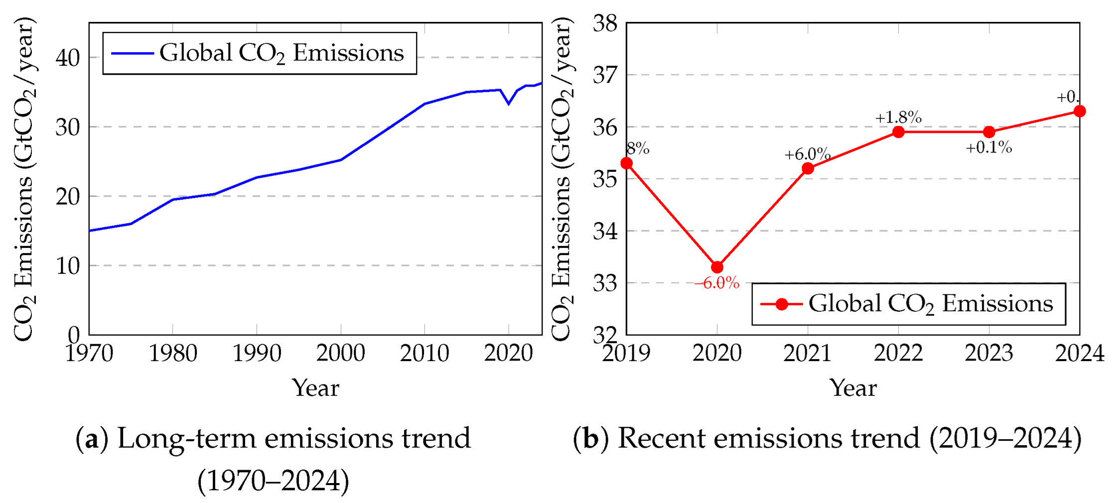
Figure 3.
PRISMA flow diagram for systematic literature selection process.
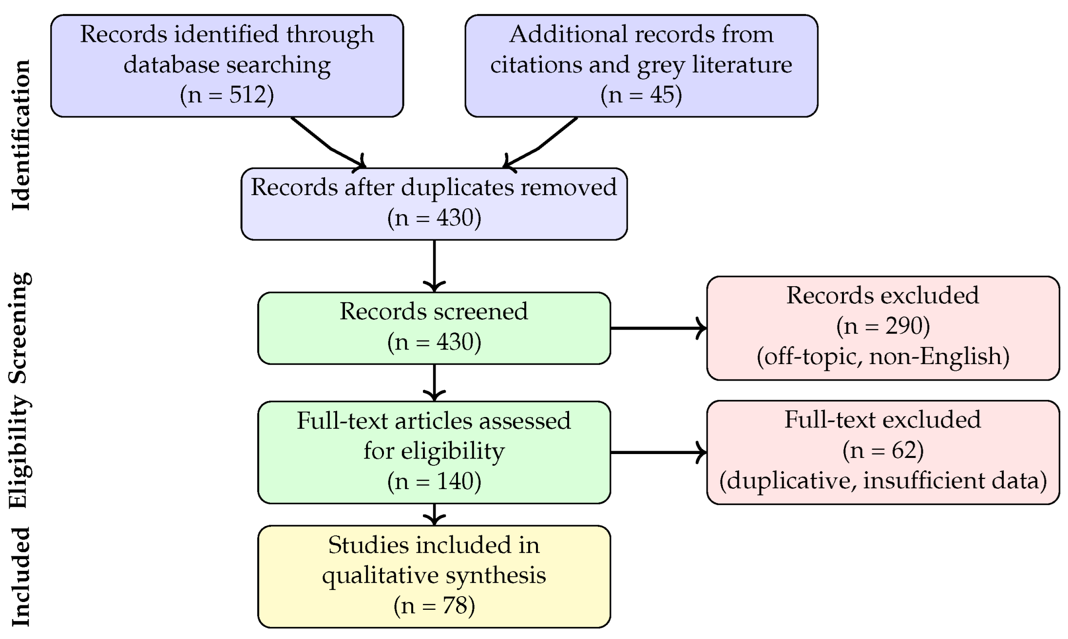
Figure 4.
Positioning of this review relative to existing WBG literature. This work uniquely spans from fundamental device technology through system-level integration while incorporating emerging technologies (vertical GaN, BDS, UWBG materials). The dashed rectangle indicates the comprehensive coverage achieved by our bottom-up systematic approach.
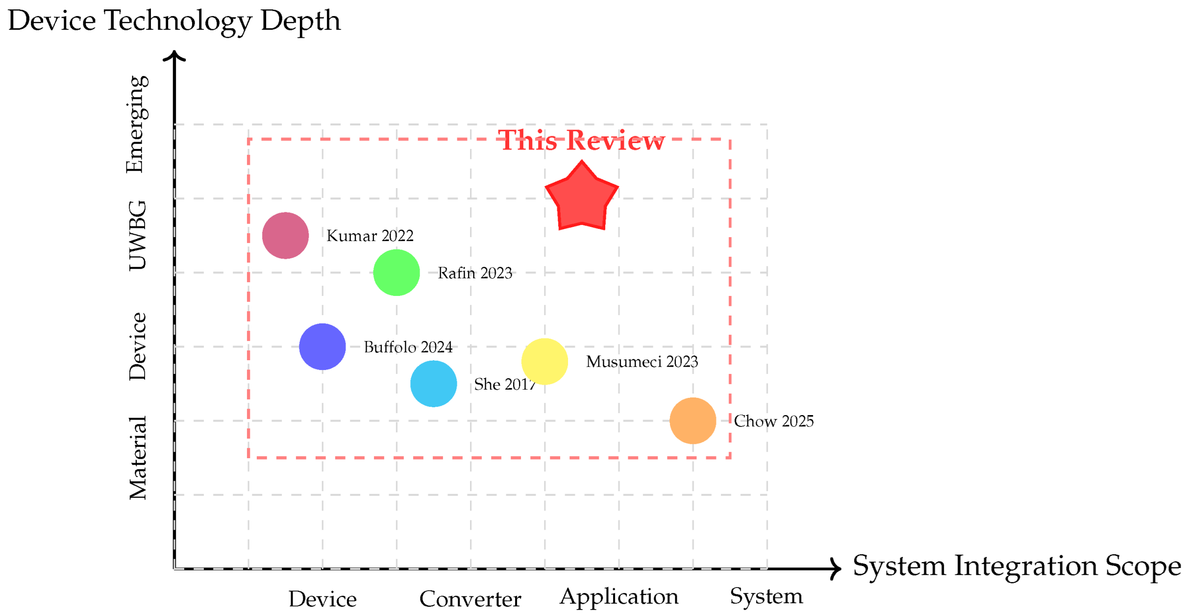
Figure 5.
Radar chart comparison of power semiconductor materials. Normalized performance relative to Si (adapted from [3,4]).
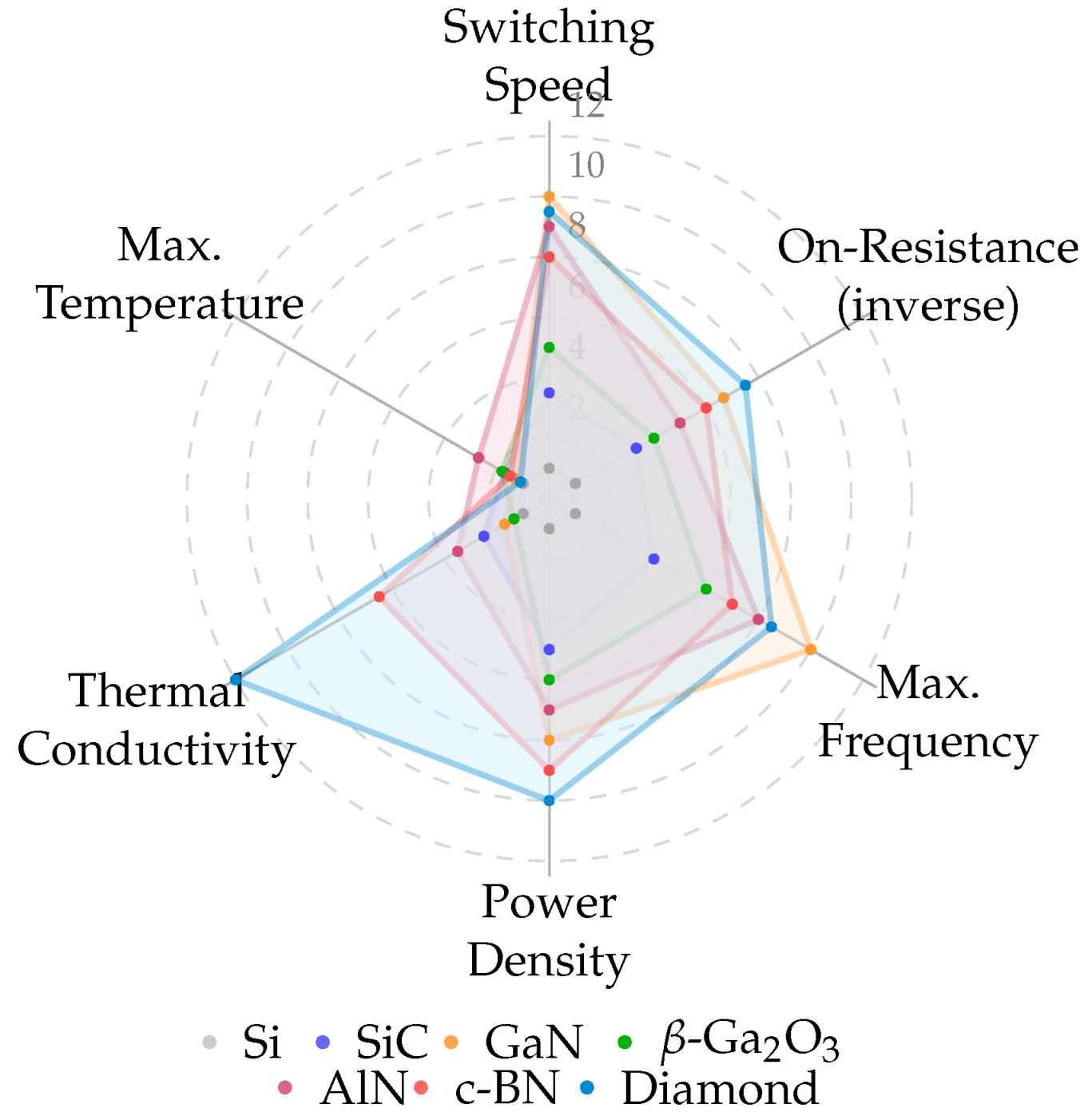
Figure 6.
Classification of SiC power devices
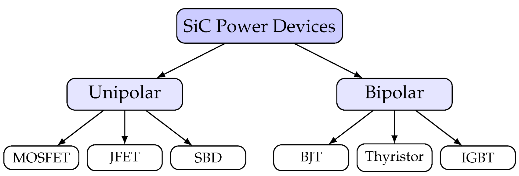
Figure 7.
Planar SiC MOSFET and Trench SiC MOSFET Structures
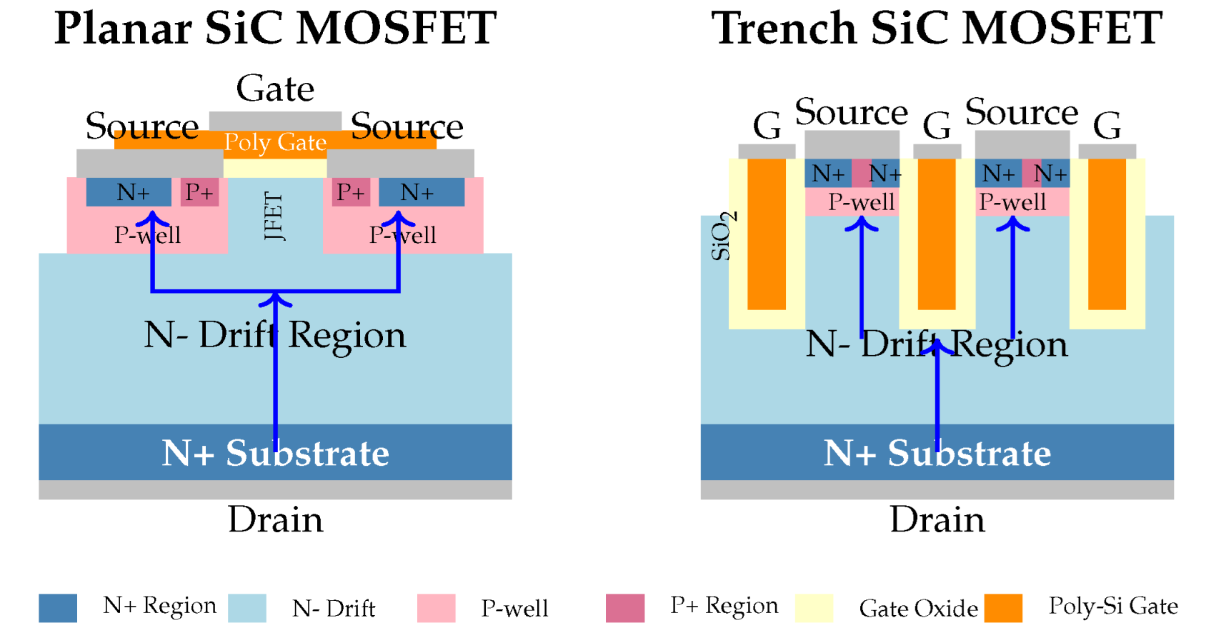
Figure 8.
Classification of GaN HEMTs devices.
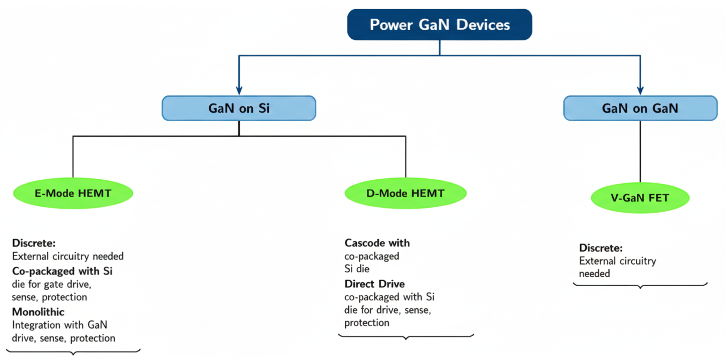
Figure 9.
Different types of GaN devices: Normally-on (d-mode), Normally-off Cascode (d-mode), Direct Drive (d-mode), Normally off (e-mode)
Figure 9.
Different types of GaN devices: Normally-on (d-mode), Normally-off Cascode (d-mode), Direct Drive (d-mode), Normally off (e-mode)
Figure 10.
GaN D-Mode Internal Structure
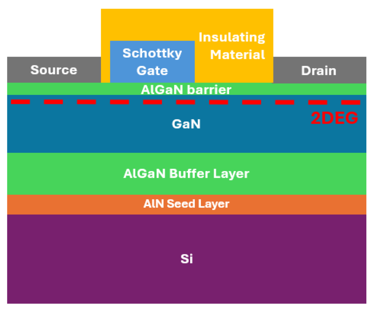
Figure 11.
GaN E-Mode Internal Structure
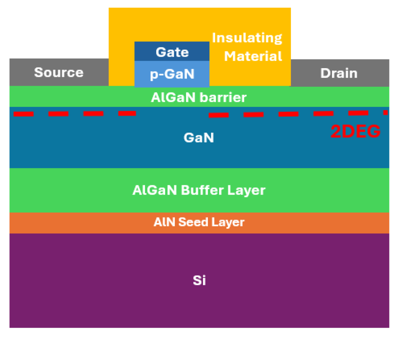
Figure 12.
SiC-based three-phase traction inverter for electric vehicle applications, adapted from [55].
Figure 12.
SiC-based three-phase traction inverter for electric vehicle applications, adapted from [55].
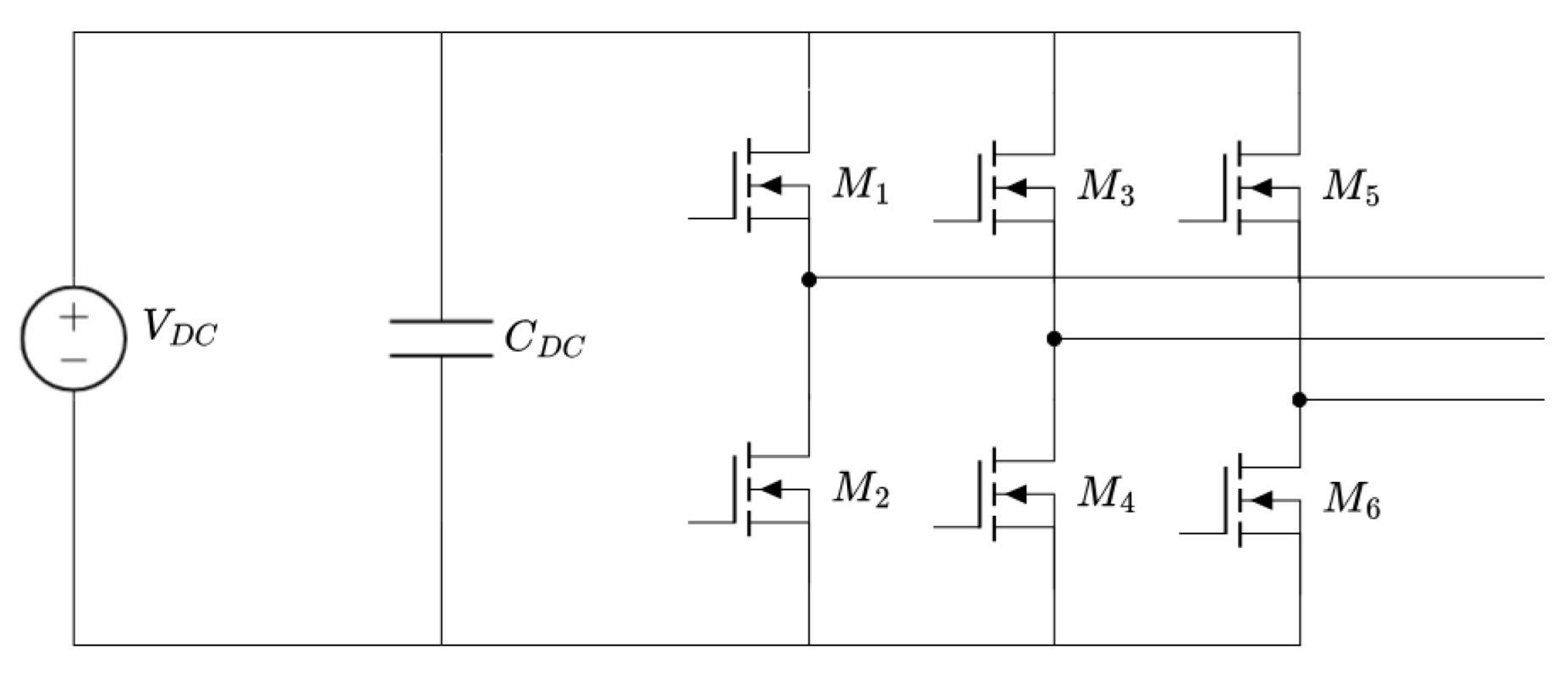
Figure 13.
SiC-based DC fast charging architecture: Vienna rectifier PFC front-end with isolated DC-DC converter, adapted from [26].
Figure 13.
SiC-based DC fast charging architecture: Vienna rectifier PFC front-end with isolated DC-DC converter, adapted from [26].
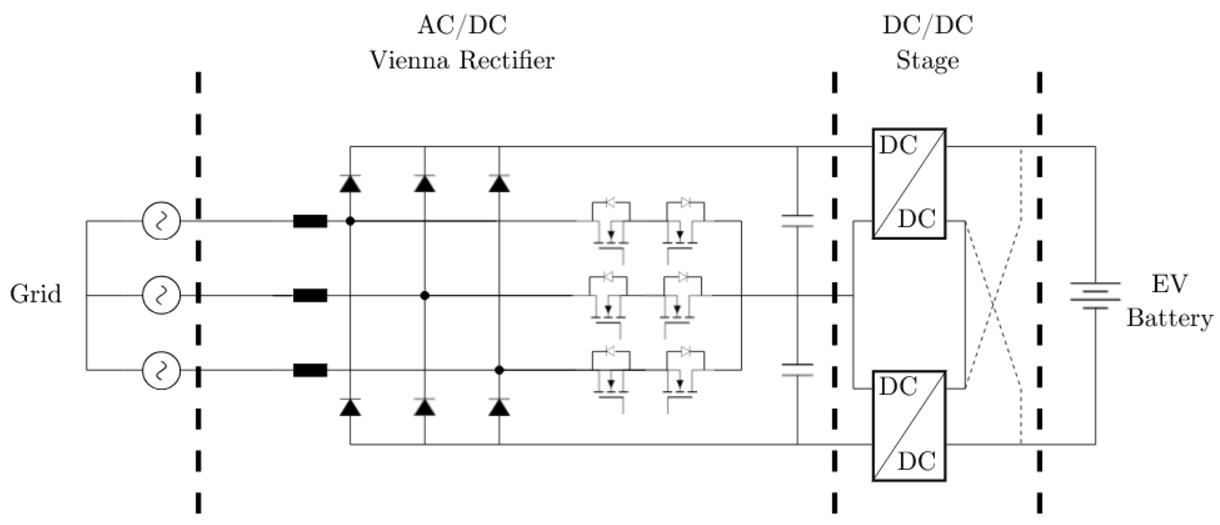
Figure 14.
SiC-based T-type three-level inverter for grid-tied PV applications, adapted from [57]
Figure 14.
SiC-based T-type three-level inverter for grid-tied PV applications, adapted from [57]
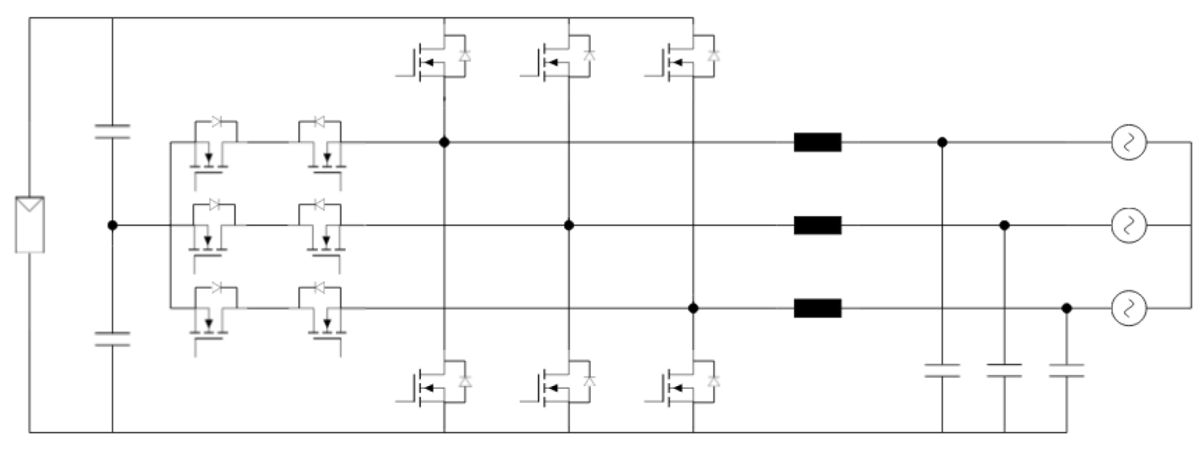
Figure 15.
Double Pulse Test Circuit
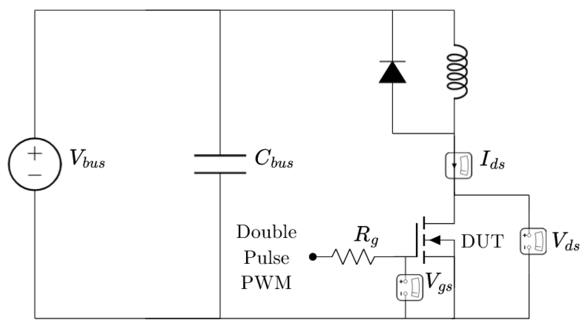
Figure 16.
Classical DPT waveforms for power devices (SiC/GaN)
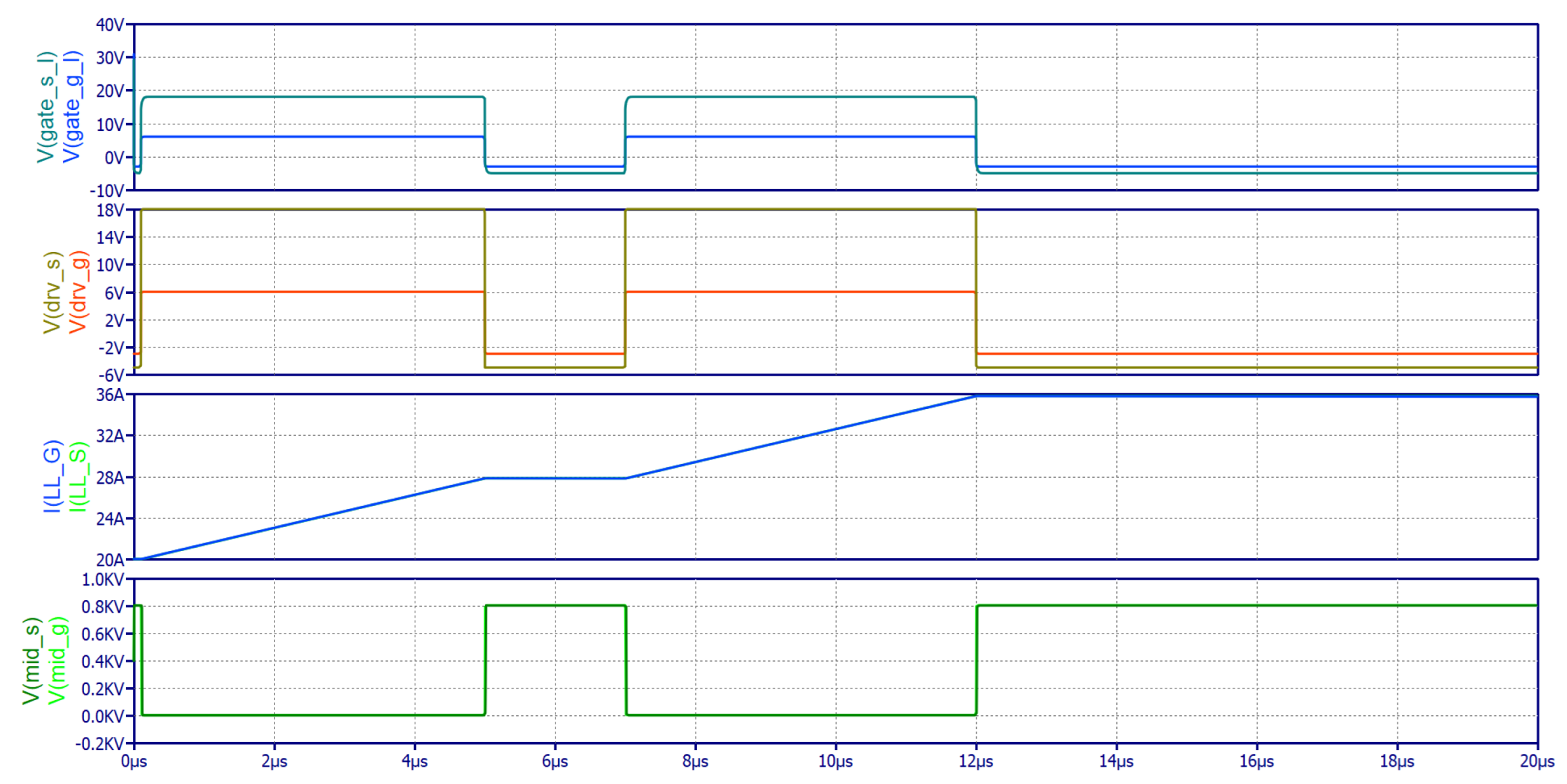
Figure 17.
Comprehensive switching dynamics comparison showing drain-source voltage, drain current, gate-source voltage, instantaneous power dissipation, and slew rates during turn-on transition at 800 V/20 A.
Figure 17.
Comprehensive switching dynamics comparison showing drain-source voltage, drain current, gate-source voltage, instantaneous power dissipation, and slew rates during turn-on transition at 800 V/20 A.
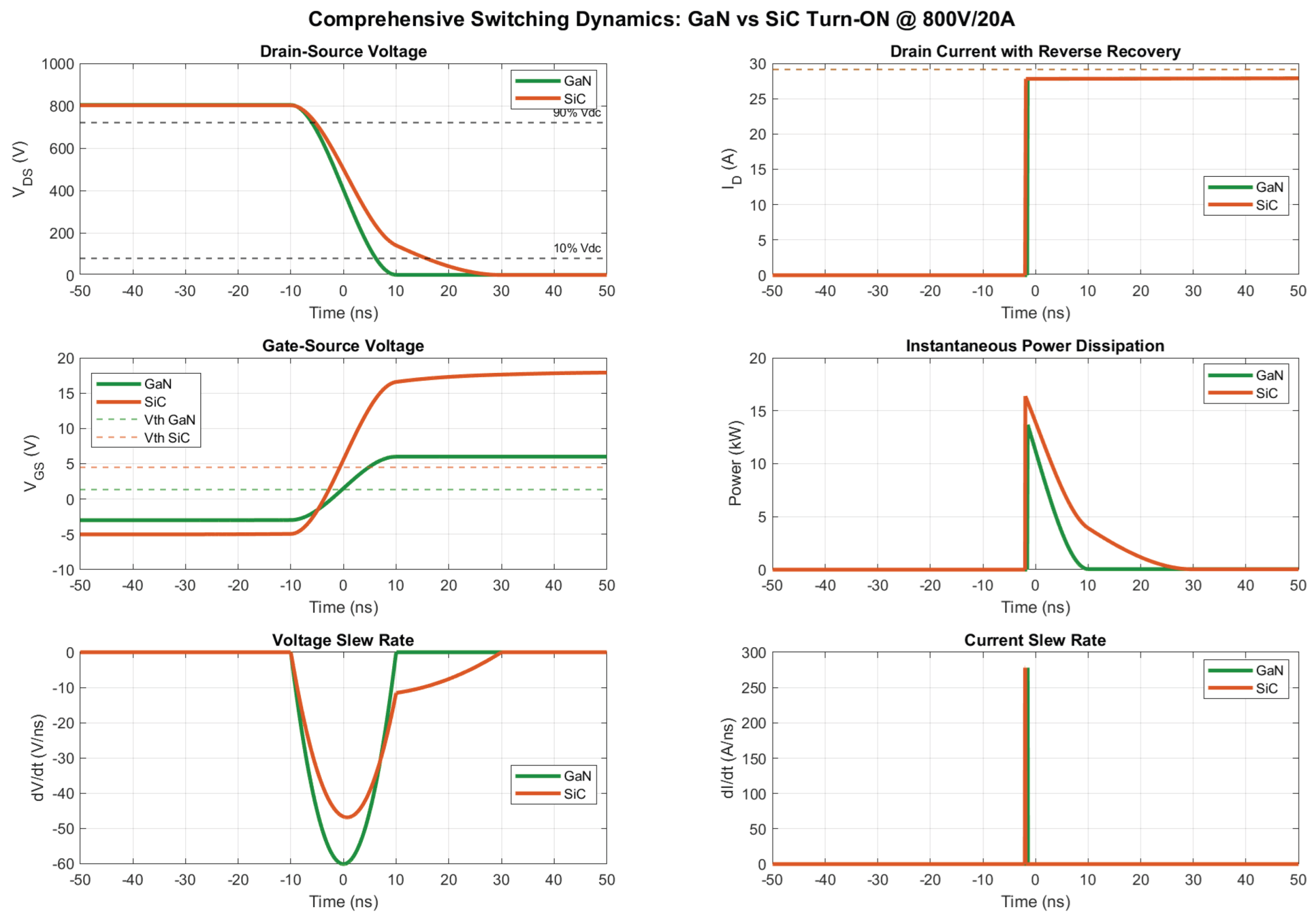
Figure 18.
System-level performance dashboard comparing fall time, slew rates, switching energy, power loss breakdown, efficiency, and figure of merit between GaN and SiC at 100 kHz operation.
Figure 18.
System-level performance dashboard comparing fall time, slew rates, switching energy, power loss breakdown, efficiency, and figure of merit between GaN and SiC at 100 kHz operation.
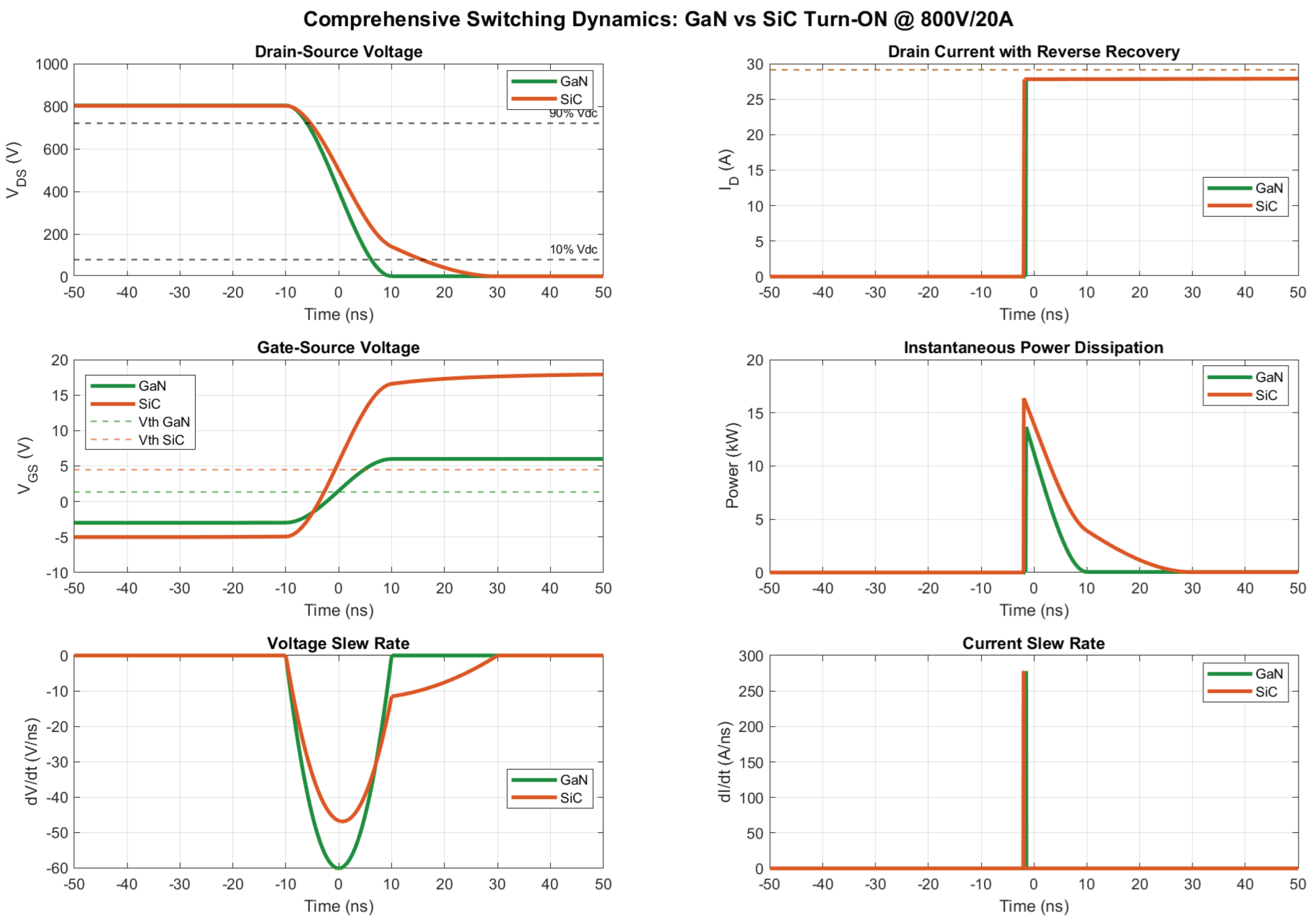
Figure 19.
Thermal performance analysis showing power loss scaling with frequency, junction temperature projection, power budget breakdown at 100 kHz, and die-level power density comparison.
Figure 19.
Thermal performance analysis showing power loss scaling with frequency, junction temperature projection, power budget breakdown at 100 kHz, and die-level power density comparison.
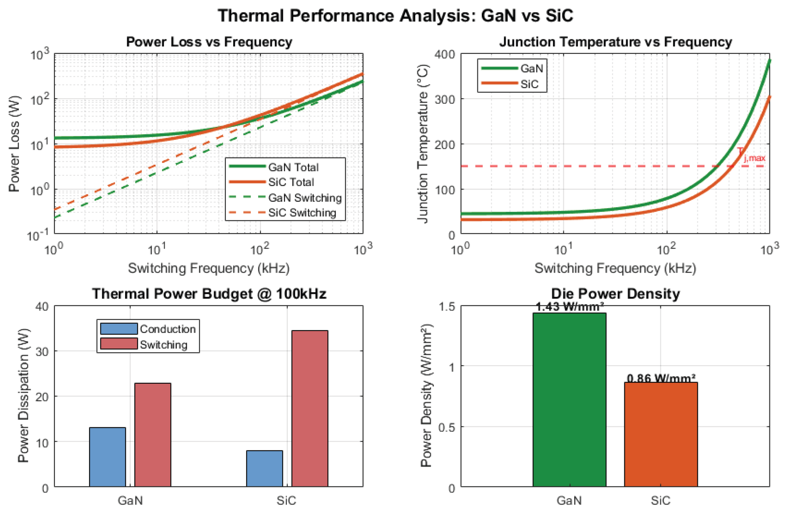
Figure 20.
Application landscape for WBG power devices.
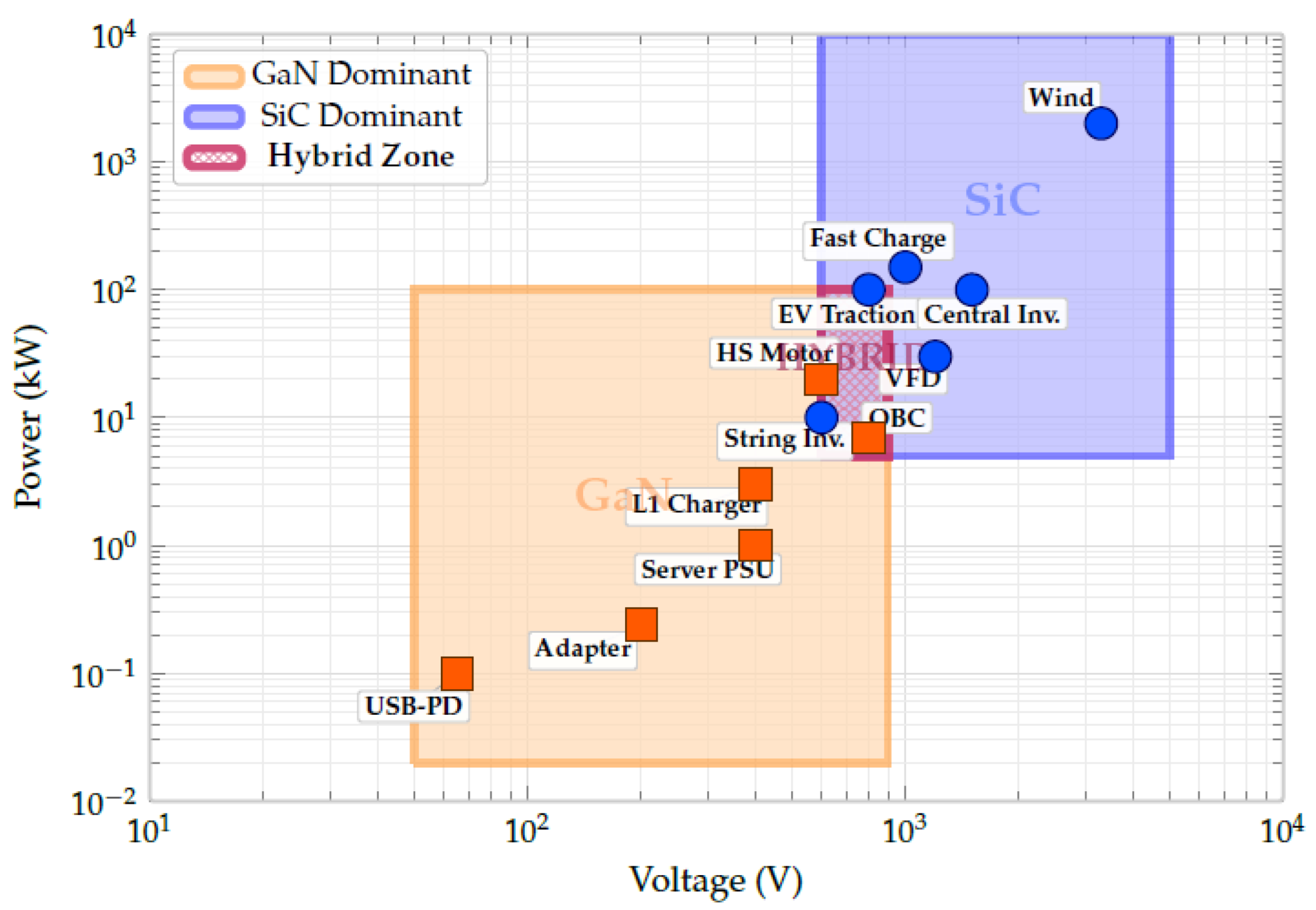
Table 1.
Distribution of Reviewed Literature by Category
| Category | Papers Reviewed | Key Focus Areas |
|---|---|---|
| SiC Device Technology | 12 | MOSFET structures, trench devices, reliability, failure modes |
| GaN HEMT Technology | 13 | E-mode/D-mode, dynamic , trapping effects |
| Converter Topologies | 10 | DAB, Buck, Inverters, Magnetics, Wireless Power |
| System Applications | 14 | EV Traction, Hydrogen, Data Centers, Solar |
| UWBG Materials | 12 | Ga2O3, AlN, Diamond, c-BN, Heterostructures |
| EMI, Thermal & Pkg | 11 | Gate drivers, layout, thermal management, packaging |
| Emerging Technologies | 3 | Vertical GaN, Fin-JFETs |
| Fundamentals & Surveys | 3 | Figures of Merit, Methodology, Historical Trends |
| Total | 78 | — |
Table 2.
Comparison with Recent WBG Semiconductor Review Papers.
| Review Paper | Year | Scope | Strengths | Limitations |
|---|---|---|---|---|
| Buffolo et al. [8] | 2024 | Industrial SiC/GaN devices | Excellent reliability analysis; commercial device survey; trapping mechanisms | Limited topology comparison; no UWBG coverage; no economic analysis |
| Rafin et al. [14] | 2023 | WBG/UWBG overview | Broad material coverage; historical context; FOM analysis | Limited system-level analysis; no vertical GaN/BDS; no design guidelines |
| Chow et al. [15] | 2025 | Carbon neutrality focus | Sustainability perspective; policy implications; grid integration | Limited converter topology detail; no practical design constraints |
| Kumar et al. [16] | 2022 | Material properties | Comprehensive FOM analysis; device physics | Dated commercial landscape (2022); no emerging devices; limited applications |
| She et al. [17] | 2017 | SiC power devices | Deep SiC device analysis; HVDC applications; converter topologies | Pre-dates GaN maturation; no UWBG coverage; limited GaN comparison |
| Musumeci & Barba [18] | 2023 | GaN power devices | Comprehensive GaN focus; DC-DC and DC-AC applications | SiC comparison limited; no UWBG materials; no system-level KPIs |
| This Review | 2026 | System-level WBG/UWBG | See Added Value below | — |
Table 3.
Key Novelty Summary: Unique Contributions Relative to Comparative Literature
| Contribution | New Data | New Insights | New Framework |
|---|---|---|---|
| Topology Comparison (Table 9) | 9 topologies compared: VSI, Buck, DAB, Vienna, T-type/NPC, LLC, Matrix, HERIC, CSI | First systematic SiC/GaN/vGaN/BDS device selection criteria with quantitative metrics | Decision guidelines based on voltage class, power level, and switching frequency |
| Emerging Devices (Sec. Section 5.3) | vGaN: 1.2 kV/50 A with 50% loss reduction vs. lateral GaN; BDS: 650–850 V monolithic four-quadrant operation | First converter-level vGaN/BDS impact analysis on 8 topologies (Table 8); commercialization timeline 2025–2030 | Technology selection: vGaN for 650 V–1.2 kV unidirectional; BDS for bidirectional/single-stage conversion |
| UWBG Materials (Sec. Section 3) | -Ga2O3: 4” wafers, 2.3 kV; AlN: 7.3 MV/cm; Diamond: 4.6 kV SBD; c-BN: 6.4 eV bandgap | TRL assessment (2–6); projected commercialization: -Ga2O3 2027–30, AlN/Diamond 2030–35, c-BN ≥2035 | Material-to-application mapping: -Ga2O3 for 600 V–3.3 kV, AlN for 10 kV+/RF, Diamond for extreme power |
| Bottom-Up Framework | 6 Figure of Merits analyzed: BFOM, BHFFOM, JFOM, KFOM, CHFFOM, TFOM (Table 5) | Clear traceability from material properties (, , , ) through device FOMs to system-level KPIs | 4-tier methodology: Materials → Devices → Converters → Systems; PRISMA-compliant review |
| Economic Analysis (Table 14) | 6 sectors: Data center ($450k/yr), EV (+20 km), Solar PV ($35k/yr), Industrial VFD ($22k/yr), Telecom ($8k/site), Aerospace (−15 kg) | Payback periods: 1.5 yr (data center), 2 yr (solar), 2.5 yr (industrial); immediate ROI for EV range and aerospace weight | Sector-specific efficiency gains: 94→97% (data center), 96→99% (EV traction), 92→95% (telecom) |
| Design Constraints (Sec. Section 10) | Dynamic : 2–5× degradation; instability; short-circuit withstand: GaN <1 s, SiC 2–5 s | 8 mitigation strategies: negative gate bias, active Miller clamping, desaturation detection (<200 ns), optimized buffer designs | Gate driver requirements matrix (Table 11): , , propagation delay, CMTI |
Table 4.
Material Properties of Semiconductors for Power Electronics, data taken from [3].
Table 4.
Material Properties of Semiconductors for Power Electronics, data taken from [3].
| Parameter | Si | 4H-SiC | GaN | -Ga2O3 | AlN | c-BN | Diamond |
|---|---|---|---|---|---|---|---|
| (eV) | 1.12 | 3.23 | 3.4 | 4.9 | 6.2 | 6.4 | 5.5 |
| (MV/cm) | 0.3 | 2.5 | 3.3 | 8 | 15 | 12 | 10 |
| (cm2/Vs) | 1440 | 950 | 2000 | 250 | 850 | 200 | 4500 |
| ( cm/s) | 1.0 | 2.0 | 2.4 | 1.1 | 1.4 | 2.0 | 2.3 |
| (W/cmK) | 1.5 | 3.7 | 2.5 | 0.1–0.3 | 2.85 | 13 | 23 |
Table 5.
Normalized Figures of Merit for Power Semiconductor Materials (Si = 1) data taken from [3,30,33].
| Material | BFOM | BHFFOM | JFOM | KFOM | CHFFOM | TFOM |
|---|---|---|---|---|---|---|
| Si | 1 | 1 | 1 | 1 | 1 | 1 |
| 4H-SiC | 317 | 13.7 | 20 | 4.8 | 29 | 3.3 |
| GaN | 846 | 27.5 | 33 | 1.4 | 56 | 2.2 |
| -Ga2O3 | 3444 | 10.5 | 14 | 0.9 | 30 | 0.8 |
| AlN | 3360 | 57.6 | 68 | 13.8 | 562 | 9.2 |
| Diamond | 50000 | 81.2 | 163 | 46.2 | 2114 | 33 |
Table 6.
UWBG Materials Development Status and Commercialization Timeline.
| Parameter | -Ga2O3 | AlN | c-BN | Diamond |
|---|---|---|---|---|
| Wafer Size (Comm.) | 4-incha | 4-inch | N/A | 2-inch |
| Best Device | 2.3 kV | 2.2 kV | N/A | 4.6 kV |
| TRL Levelb | 5–6 | 3–4 | 2–3 | 3–4 |
| (eV) | 4.9 | 6.2 | 6.4 | 5.5 |
| (W/cmK) | 0.1–0.3 | 2.85 | 13 | 22–23 |
| Primary Challenge | Low | Doping/Contacts | Substrate size | n-type doping |
| Target Applications | 600V–3.3kV | 10kV+, RF | >10kV, extreme | Extreme power |
| Projected Commerc.c | 2027–2030 | 2030–2035 | ≥2035 | 2030–2035 |
a 4-inch substrates in limited commercial production; 2-inch widely available.
b TRL per Horizon 2020 Work Programme (European Commission, 2014): TRL 5 = technology validated in relevant environment; TRL 6 = technology demonstrated in relevant environment.
c Projected dates represent estimated initial commercial device availability; confidence decreases for longer-term projections.
| Parameter | GaN HEMT | GaN Cas. | SiC MOS | Si IGBT |
|---|---|---|---|---|
| Voltage (V) | 600–650 | 600–900 | 650–3300 | 600–6500 |
| Current (A) | 1–90 | 10–60 | 5–200 | 10–3600 |
| (mcm2) | 1–5 | 3–8 | 3–15 | — |
| Max (MHz) | 1–40 | 0.5–10 | 0.1–2 | 0.02–0.1 |
| (V/ns) | 50–200 | 30–100 | 20–100 | 1–20 |
| (nC) | 1–20 | 10–50 | 20–300 | 100–5000 |
| Max (°C) | 150–175 | 150 | 175–200 | 175 |
| Rev. Recovery | None | Limited | Moderate | V. High |
| FOM () | Best | Good | Good | Poor |
| Cost ($/A) | Medium | Med-High | High | Low |
Table 8.
GaN Technology Evolution: Impact on Converter Topologies vs. Established SiC.
| Topology | Current SiC Solution | Vertical GaN Potential | GaN BDS Potential | Timeline |
|---|---|---|---|---|
| Traction Inverter | 1.2 kV SiC MOSFET, 10–20 kHz | 1.2 kV vGaN, 50–100 kHz, 50% lower losses | Not applicable | vGaN: 2027–2029 |
| Vienna Rectifier | Back-to-back SiC, 30–50 kHz | Higher frequency, smaller magnetics | Single-device solution, 100 kHz+ | BDS: 2025–2026 |
| DAB Converter | SiC for >50 kW, ZVS operation | Smaller transformer, higher frequency | Single-stage capability | vGaN: 2028+ |
| T-Type Inverter | Discrete SiC neutral switches | Enhanced switching speed | 50% lower , simplified drive | BDS: Available now |
| Matrix Converter | Complex discrete arrays | N/A | Revolutionary: single-device BDS | BDS: 2025–2026 |
| HERIC (PV) | Discrete Si/SiC switches | N/A | MHz operation, grid support | BDS: Available now |
| CSI Motor Drive | SiC + series diodes | Native blocking, lower losses | Native bidirectional blocking | Both: 2027+ |
| Single-Stage OBC | Two-stage (PFC + DC-DC) | N/A | Eliminates DC-link capacitor | BDS: 2025–2026 |
Table 9.
SiC vs. GaN Comparison for Major Power Converter Topologies.
| Topology | SiC Advantages | GaN Advantages | Recommended |
|---|---|---|---|
| Two-Level VSI | Higher voltage (1.2–3.3 kV), better thermal | Lower switching losses, smaller passives | SiC (>100 kW) |
| Buck (<1 kW) | Better thermal margin | 10× lower , MHz operation | GaN |
| Buck (>10 kW) | Higher current handling | Lower switching losses at 100–500 kHz | SiC |
| Interleaved | Better current sharing, thermal stability | Phase current cancellation, smaller magnetics | Application dependent |
| DAB (<20 kW) | Wide ZVS range | >500 kHz, smaller transformer | GaN |
| DAB (>50 kW) | 1.2 kV/>100 A devices | Lower turn-off losses | SiC |
| Vienna Rectifier | Higher voltage margin | Lower THD with higher | GaN (<30 kW); SiC (>30 kW) |
| T-Type/NPC | 1700 V devices for 1500 V PV | BDS enables single-package solution | GaN (resid.); SiC (utility) |
| LLC Resonant | Wide input range, stable | Very low , enables >1 MHz | GaN |
Table 10.
Thermal Properties of Wide-Bandgap Semiconductors for Power Electronics
| Property | SiC (4H) | GaN | AlN |
|---|---|---|---|
| Thermal conductivity (W/mK) | 330–490 | 130–200 | 285–320 |
| Max. junction temperature (°C) | >200 | 150–175 | >200 |
| Bandgap (eV) | 3.26 | 3.4 | 6.2 |
| Thermal coeff. of | Strongly negative |
| Parameter | Si MOSFET/IGBT | SiC MOSFET | GaN HEMT |
|---|---|---|---|
| Turn-on | +10 to +15 V | +15 to +20 V | +5 to +6 V |
| Turn-off | 0 V | −3 to −5 V | 0 V |
| Gate Charge () | 50–500 nC | 20–100 nC | 1–10 nC |
| Peak Drive Current | 1–4 A | 4–10 A | 1–5 A |
| Propagation Delay | 50–200 ns | 20–50 ns | <20 ns |
| Immunity | 10–50 V/ns | 50–150 V/ns | 100–300 V/ns |
| Negative Bias Req. | Optional | Required | Not Required |
| Miller Plateau | Flat, defined | Higher, not flat | Low, fast |
| Range | 2–4 V | 1.5–4 V | 1–2 V |
Table 14.
Economic Benefits of WBG Adoption Across Application Sectors.
| Sector | Application | Impr. | Savings | Payback |
|---|---|---|---|---|
| Data Center | Server PSU (10 MW) | 94→97% | $450k/yr | 1.5 yr |
| EV | Traction inverter | 96→99% | +20 km | Immed. |
| Solar PV | String inv. (1 MW) | 96→98.5% | $35k/yr | 2 yr |
| Industrial | Variable Frequency Drive (VFD) (500 kW) | 95→98% | $22k/yr | 2.5 yr |
| Telecom | 5G base station | 92→95% | $8k/site | 1.8 yr |
| Aerospace | Aux. power unit | 93→97% | −15 kg | Immed. |
Table 15.
Key Performance Indicators: Silicon vs. WBG Comparison, data taken from [8].
Table 15.
Key Performance Indicators: Silicon vs. WBG Comparison, data taken from [8].
| KPI | Silicon | WBG |
|---|---|---|
| Peak efficiency () | 94–97% | 98–99.5% |
| Power density | 3–8 kW/L | 15–50 kW/L |
| Specific power | 2–5 kW/kg | 8–20 kW/kg |
| Switching frequency () | 20–100 kHz | 0.2–2 MHz |
| Maximum junction temp. () | 150°C | 175–200°C |
| Total harmonic distortion (THD) | 3–8% | 1–3% |
| Voltage slew rate () | 5–15 kV/s | 50–200 kV/s |
| Current slew rate () | 1–5 kA/s | 10–50 kA/s |
Table 16.
Multiphysics trade-off analysis for 10 kW inverter upgrade
| Parameter | Si IGBT (8 kHz) | SiC MOSFET (100 kHz) |
|---|---|---|
| Switching losses | 180 W | 45 W |
| Gate drive power | 0.8 W | 4.2 W |
| EMI filter volume | 1.2 L | 0.4 L |
| EMI filter cost | $45 | $120 |
| PCB layer count | 4 | 6 |
| Motor dv/dt stress | 2.5 kV/s | 15–25 kV/s |
Table 17.
PCB cost breakdown for high-frequency GaN design
| Design Aspect | Conventional | GaN 500 kHz |
|---|---|---|
| Layer count | 4 | 6 |
| Copper weight (inner) | 1 oz | 2 oz |
| Via technology | Standard | Filled/capped |
| Impedance control | No | Yes |
| PCB cost per unit | $12 | $38 |
Table 18.
WBG Device Adoption in Electric Vehicle Applications, data taken from [11].
Table 18.
WBG Device Adoption in Electric Vehicle Applications, data taken from [11].
| OEM | Model | Tech | Application | Perf. Gain | Year |
|---|---|---|---|---|---|
| Tesla | Model 3/Y | SiC | Traction Inverter | +8% range | 2017 |
| BYD | Han EV | SiC | Traction + OBC | +5% efficiency | 2020 |
| Lucid | Air | SiC | 900V Inverter | +10% range | 2021 |
| Hyundai | IONIQ 5 | SiC | 800V Charging | 18 min charge | 2021 |
| Mercedes | EQS | SiC | Traction Inverter | +6% range | 2022 |
| BMW | iX | GaN | OBC | 40% size red. | 2022 |
| Porsche | Taycan | SiC | 800V System | 270kW charge | 2019 |
| VW | ID.7 | SiC | APP310 Inv. | +5% efficiency | 2023 |
Table 19.
Parasitic Inductance Comparison for Different Packages, data taken from [58].
Table 19.
Parasitic Inductance Comparison for Different Packages, data taken from [58].
| Package | (nH) | (nH) | (pF) | Max Range |
|---|---|---|---|---|
| TO-247 | 10–15 | 5–10 | 5–10 | <100 kHz |
| D2PAK | 5–8 | 3–5 | 3–5 | <500 kHz |
| SMD (GaN) | 0.5–2 | 1–3 | 1–2 | >1 MHz |
| Chip-scale | 0.1–0.5 | 0.5–1 | 0.5–1 | >5 MHz |
| DFN (QFN) | 1–3 | 2–4 | 2–3 | 200–800 kHz |
| LGA | 0.3–1 | 0.8–2 | 1–2 | 1–3 MHz |
Disclaimer/Publisher’s Note: The statements, opinions and data contained in all publications are solely those of the individual author(s) and contributor(s) and not of MDPI and/or the editor(s). MDPI and/or the editor(s) disclaim responsibility for any injury to people or property resulting from any ideas, methods, instructions or products referred to in the content. |
© 2026 by the authors. Licensee MDPI, Basel, Switzerland. This article is an open access article distributed under the terms and conditions of the Creative Commons Attribution (CC BY) license (http://creativecommons.org/licenses/by/4.0/).
Copyright: This open access article is published under a Creative Commons CC BY 4.0 license, which permit the free download, distribution, and reuse, provided that the author and preprint are cited in any reuse.


