Submitted:
28 January 2026
Posted:
29 January 2026
You are already at the latest version
Abstract
The influence of a non-resonant intense laser field on the optical absorption and Raman scattering processes in ZnO/Mg0.2Zn0.8O quantum wells is theoretically investigated. It is shown that the dressing field significantly modifies the confinement potential and reshapes the electronic wave functions, leading to tunable shifts in intersubband transition energies and changes in the dipole matrix elements. These laser-induced effects produce notable variations in the absorption spectrum and strongly modulate the Raman differential cross section and Raman gain. Under the application of the non-resonant laser field, the Raman gain is enhanced by almost a factor of four, whereas off-resonant pumping results in much weaker but still field-dependent responses. The results demonstrate that intense laser fields provide an effective tool to dynamically control the optical and Raman properties of ZnO-based quantum well structures.
Keywords:
ZnO/MgZnO quantum wells
; non-resonant intense laser
; linear optical absorption
; Raman differential cross section
; Raman gain
1. Introduction
Semiconductor quantum wells (QWs) are of high importance in the investigation of nanophotonics and optoelectronic devices due to their quantized electron states and highly tunable optical properties. Among the multiple QW systems that can be found in the literature, the ZnO-based heterostructures have been receiving great attention in the last decades due to their prominent optical properties in the blue-ultraviolet (UV) region of the spectrum [1,2,3], wide bandgap semiconductivity, advantages in fabrication, native defects [4], large exciton binding energy [5], and other thermal, optical, and electronic properties.
The intrinsic features of the ZnO-based systems make them suitable for many applications, such as terahertz (THz) technologies [6], quantum Hall effect (QHE) devices [7], High Electron Mobility Transistors (HEMTs) [8], heterojunction photodiodes (HPDs) [9], light-emitting diodes (LEDs) [10], etc. Particularly, in the development of ZnO-based heterostructures, MgxZn1−xO alloys have been widely investigated and employed for optoelectronic devices thanks to their tunable and higher bandgap structure [11], which goes from 3.37 eV in ZnO to 7.8 eV in MgO; furthermore, the Mg doping does not cause great lattice distortion and produces further adjustments in the carrier concentration and decreases leakage current [12].
Among ZnO-based heterostructures, ZnO/MgxZn1−xO QWs are of typical interest due to their confinement properties, which allow an increase in the concentration of localized 2D electron gas [13] and enhanced electron mobility (up to 20 cm2/ V) [14]. These structures are well produced via multiple growth methods, such as molecular beam epitaxy, thermal vapor deposition, and pulsed laser deposition [15,16,17], and they present a very important feature: ZnO/MgZnxO1−x QWs exhibit significant spontaneous and piezoelectric polarization along the c-axis [18,19,20], which strongly modifies the confinement potential due to these built-in electric fields.
Beyond material composition, optoelectronic and additional properties of heterostructures are strongly influenced by the geometry and dimensions of the confinement potential. This feature has been largely demonstrated in the study of quantum dots (QDs) systems, particularly in GaAs-based nanostructures, which serve as a well-founded benchmark for low-dimensional confinement effects. For example, Gil-Corrales et al. in 2025 [21] studied the effects of different configurations (size and shape) on confined non-interacting particles that influence the thermodynamic features of GaAs QDs, resulting in practical properties for optical and Raman devices. Furthermore, in 2026 [22] again in three-dimensional systems, has been analyzed the additional effect of external electric fields and nonextensive statistics in QDs. These works tells that the confinement engineering, including geometrical design or external perturbations are central in controlling quantum states in semiconductor heterostructures.
Due to this, there has been a vast and in-depth study of the effects of external laser fields in multiple systems based on heterostructures. Specifically, the study of non-resonant intense laser fields (ILFs) has become a major focus of recent research in condensed matter, mainly due to the tailoring of optical and electronic properties resulting from the tunability of the confinement potential along the laser polarization direction [23]. For example, Wang et al. in 2021 [24] reported the tailoring effect of external fields via a terahertz ILF on the shallow-donor-related photoionization cross section in GaAs bulk semiconductors. Donado et al. in 2025 [25] reported the particular effect of combining an external electric field and an ILF on the electronic properties of a truncated cone quantum dot, in which the quantum confinement can be controlled by the dressing parameter . Additionally, Dagua et al. in 2025 [26] reported the effects of ILF on the probability of electronic transmission in QW AlGaAs/GaAs resonant tunneling diodes based on the Pösch-Teller potential.
All of the effects on the quantum confinement properties of a heterostructure will have a noticeable impact on optical absorption, which plays an important role in the characterization of these systems. In the case of the ZnO-based heterostructures, Tang et al. in 2025 [27] investigated the generation of double peaks in the inter-band and inter-subband optical absorption in MgxZn1−xO/ AlyGa1−yN core-shell nanowires, depending on the core radius and different crystal phases, while Gu et al. in 2022 [28] reported the shift of the peak positions in the total optical absorption coefficient in MgZnO/ZnO double QWs due to the variation of external electric and magnetic fields. As additional literature, Andrzejewski et al. in 2021 [29] carried out the experimental measurement and theoretical comparison of the photoluminescent spectra of multiple grown asymmetric QWs with different widths and internal electric fields, considering single particle transitions and localized excitonic contributions to the photoluminescence depending on temperature. Lastly, Atic et al. in 2024 [30] showed numerically how the Mg concentration and doping density affect the inter-subband absorption peak and tunneling current in different configurations of multiple ZnO/MgZnO QWs and resonant-tunneling structures in order to mimic the active regions of a quantum cascade laser.
Additionally, there are modifications to the light-matter interactions as a result of quantum confinement and changes in the electronic density of the system. One of these phenomena is the inelastic scattering of incident photons due to their interaction with electrons, which produces emitted radiation at shifted frequencies depending on the type of transition occurring in the system (Stokes/anti-Stokes) [31,32]. These processes are known as Raman processes, which can be effectively characterized using the differential cross section (DCS) of electron Raman scattering. The DCS quantifies the probability per solid angle and per unit frequency interval that an incident photon will be scattered, serving to determine the subband structure and electron density distribution in heterostructures. For example, Mojab-Abpardeh et al. in 2018 [33] performed the theoretical calculation of the DCS in the strained ZnO/MgZnO double QWs, successfully determining the impact of the system dimensions on the presence of new peaks in the cross-section. More recently, Betancourt-Riera et al. in 2025 [34] reported the effect of an external electric field on the Raman emission spectra for intersubband transitions in semiconductor nanowires.
Another important feature that characterizes the Raman process is the gain coefficient, which measures how a heterostructure amplifies an optical probe via stimulated Raman scattering when pumped by a strong optical field. Since the Raman gain is directly related to the imaginary part of the third-order susceptibility, it is prone to being affected by nonlinearities in the system. For example, Tiutiunnyk et al. in 2020 [35] studied the effect of asymmetric step-like InGaAs/GaAs QWs on the enhancement of the Raman gain, especially with the inclusion of conduction-band non-parabolicity that permits a direct comparison of deviations with the most traditional parabolic models. Furthermore, Elamathi et al. in 2020 [36] calculated the impact of hydrostatic pressure and geometric confinement on the nonlinear optical properties of a confined exciton in InP/ZnS core/shell quantum dots, including the shift of the Raman intensity toward a higher Raman gain due to applied hydrostatic pressure.
Although Raman scattering in nanomaterials and nanostructures has been extensively investigated, systematic and recent studies of the Raman differential cross section and Raman gain in ZnO/MgZnO quantum well systems remain scarce and difficult to find. However, it is still possible to find some related works on Raman scattering in ZnO-based structures. Among the mentioned works, Tran et al. in 2022 [37] reported the successful fabrication of surface-enhanced Raman spectroscopy substrates based on ZnO/Au nanorods, which offer great signal enhancement and can be further amplified under UV excitation. Additionally, Samriti et al. in 2024 [38] also reported the excellent performance of ZnO/Ag nanohybrid substrates for surface-enhanced Raman scattering applications.
In the present work, we investigated the modification of confinement properties, linear optical absorption, Raman DCS and Raman gain in a ZnO/Mg0.2Zn0.8O QW with internal electric fields under the influence of a non-resonant ILF. Through the theoretical framework of the envelope function approximation, considering fixed temperature, piezoelectric and spontaneous polarization, and dressing-dependent carrier densities, we examine how the dressing parameter alters the confined energy levels, dipole matrix elements, optical absorption coefficient, and lastly the Raman DCS and Raman gain. These results highlight the potential for optical field tailoring of QW properties, paving the way for the development of tunable photonic devices of ZnO-based systems.
This paper is organized as follows: In Section 2, we schematize the system and the theory, including the main equations used for the dressed potential, optical absorption, DCS, and Raman gain. In Section 3, our main results are presented and discussed. Finally, in Section 4, we present our concluding remarks.
2. Theory
2.1. ZnO/MgxZn1−xO Heterostructure
The system consists of an asymmetric Quantum Well, where the well (ZnO) and the barriers (MgxZn1−xO) have dimensions of nm and nm, respectively, the concentration of Mg has been fixed at , see Figure 1. Following [39], the total potential U consists of two parts: the band offset and the built-in electric fields resulting from piezoelectric and spontaneous polarization, and is given by:
where z is the growth direction of the structure, , are the values of the built-in electric fields inside the well and the barrier, respectively, is the conduction band discontinuity and L is the total length of the system. These internal electric fields are calculated by
where is the total contribution from piezoelectric and spontaneous polarization in the whole system, and are the dielectric constants for the well and barrier, respectively. Additionally, the band discontinuity can be defined as a percentage of the difference between the bandgaps in the junction, for this case
where is the MgxZn1−xO/ZnO band offset, which is a typical value according to the literature (citar papers). The multiple parameters used for the heterostructure, including the dependencies on the Mg concentration, internal electric fields and band discontinuity values, can be found in Table 1. The corresponding values of ZnO can be obtained by putting .
2.2. Non-Resonant Intense Laser Field (ILF) and Schrödinger Equation
In the presence of a non-resonant intense laser field (ILF), the interaction between the confined electron in the heterostructure and the incident electromagnetic field can be treated semi-classically, making use of the Kramers-Henneberger transformation, which transfers the time-dependence of the Hamiltonian to the confinement potential through an oscillating argument (gilcorralestesis). Considering a high frequency incident field compared to the proper frequencies for the system’s transitions, the time-dependent effect of the potential can be turned into a laser-dressed potential obtained by the period average of the oscillating potential. In this context, the Schrödinger equation for the electron in the QW, under the envelope function approximation, is given by [40],
where ℏ is the reduced Planck constant, represents the effective mass varying along the z direction, and are the wave function and energy associated with the jth state for the electron in the system. Under the mentioned approximation, the laser-dressed confinement potential V obtained from the interaction of the system with the external laser field is given by
where is the dressing laser parameter and is the non-resonant frequency of the laser field.
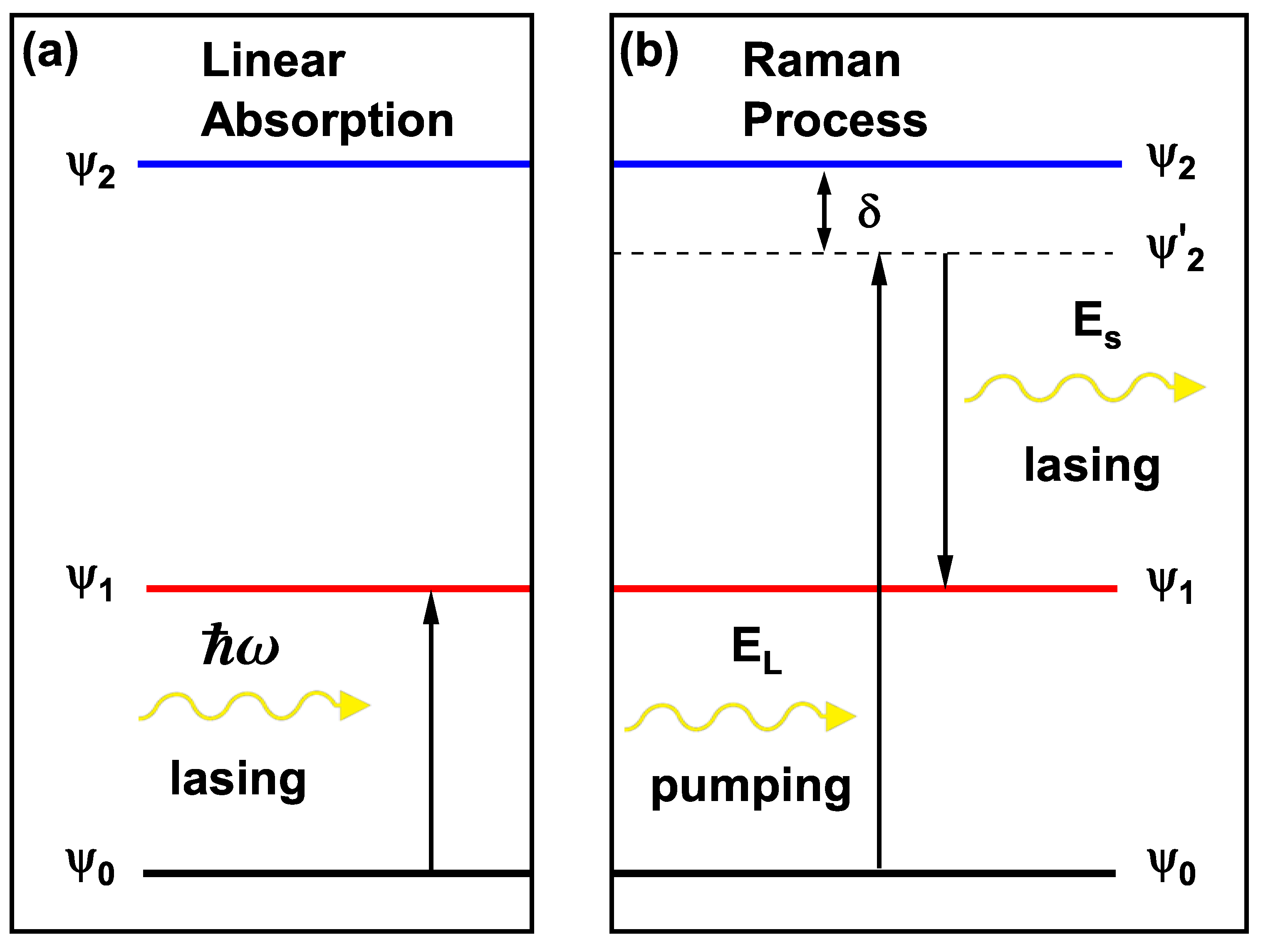
Figure 2.
Transitions in the linear optical absorption and Raman process. In (a) is represented the states and for a given value of the incident photon’s energy . In (b) is depicted the Stokes Raman process of optical pumping from to a virtual state due to the incident radiation , and the lasing of secondary radiation to reach , additional to the pump detuning between the real and virtual states.
2.3. Linear Optical Absorption Coefficient and Temperature Dependence
The absorption of an incident photon’s energy can produce a transition between and states (Figure 1(a)). This process in the system is modeled through a semi-classical interaction, where the quantum discrete states are the electronic states and the incident electromagnetic field exhibits classical behavior, allowing each electron to interact with the field and be excited to higher energy levels. Employing a matrix density formalism combined with perturbation theory, it is possible to obtain an expression for the first order susceptibility (gilcorralestesis), and from this, the standard formula for linear optical absorption, which is given by [41]
where , is the frequency of the incident photon, is the transition matrix element and the difference of volumetric carrier density between and states, respectively; is the intersubband relaxation time and are the vacuum permittivity and permeability, respectively.
Since the optical absorption depends on the volumetric carrier densities, it is important to understand and consider effects due to the laser-dressed potential and intensive properties, such as temperature, in the population of the ground and excited states. The total superficial carrier density in the system is related to temperature through the superficial carrier density for the state as , where is given by [41]
where is the energy of the state, is the Boltzmann constant, is the well effective mass, and the relation between and is used to obtain the Fermi level at temperature T. With the Fermi level known, the volumetric electronic population difference between states i and j can be calculated as,
2.4. Raman Gain Theory
For scattering in general, an important concept is the differential cross section (DCS), which for the case of the Raman scattering is given by [40]
where is the cross section, is the solid angle, , c is the vacuum speed of light, are the frequency-dependent refractive indexes, which can be considered equal; is the frequency of the incident radiation, is the frequency of the secondary radiation emitted, is the polarization vector for the emitted secondary radiation field, is the volume of the QW.
The Raman process considers two transitions: of absorption and of emission (Figure 1(b)), for which the transition rate is [40]
where and are the broadenings of the intermediate and final states, which are chosen to be [33]. Since the problem is in one dimension, the polarization vector for both the incident and the emitted secondary radiation can be taken as in the z-axis, and then, the photon-electron interaction operators are given by
The magnitude of the differential cross section can be explained in terms of the expected value of the velocity operator between the and state and the second order matrix element .
On the other hand, another important concept is the Raman gain, which is a quantity that characterizes the efficiency of the Raman scattering process for obtaining coherent emerging radiation. For the formula of gain to be obtained, it’s needed to calculate the nonlinear susceptibility given by [40]
From this, the Raman gain can be obtained using
where is the refractive index, is the frequency of the secondary radiation, is the linewidth of the susceptibility [39], and is the amplitude of the pumping or incident field which can be related with its intensity W m−2[39] by
The energy of the incident field can take a wide spectrum of values. It can be given by the physical process of electron excitation, in which it is supposed that the electron is pumped into a virtual state with energy from the ground state, before lasing the secondary radiation [42]. This is related to the real state energy through the detuning by which a value of is obtained.
3. Results
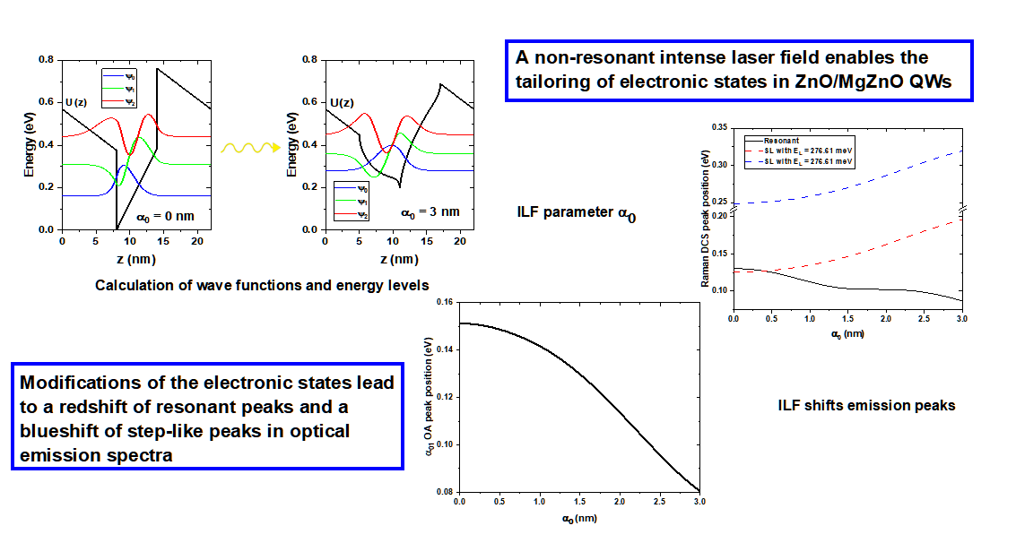
Figure 3 shows the conduction band bottom profile for a ZnO quantum well with length 6 nm, with equal Mg0.2Zn0.8O barriers of 8 nm, additionally, the effects of the internal electric fields and are included in both the barrier and well regions. In this system, the effect of an intense non-resonant laser field determined by the dressing parameter has been included. Figure 3(a) compares the modification of the potential profile of the system initially without a laser field (black curve), with a laser parameter 1 nm (red curve) and for 3 nm (blue curve).
The potential modified by the effect of the intense laser field has been calculated according to Equation (5) and modifications are evident in the interfaces between both materials with a curved characteristic, which is a typical effect of the response to an intense non-resonant laser field, also, note the decrease in the depth of the central well that is proportional to the magnitude of the dressing parameter (compare the well region for 1 nm and 3 nm). The mentioned modifications originate particular changes in the limited states of the system that imply a potential control in the optical properties, as will be mentioned later. This laser-induced symmetry directly affects the dipole matrix elements and, consequently, the allowed optical transitions.
Figure 3(b) shows the energy variation as a function of the laser parameter for the first three confined states in the quantum well system with 6 nm for the well and 8 nm for the barriers. The ground state is represented by the black line, and the first and second excited states are represented by the red and blue lines, respectively, and the Fermi level is shown in dashed lines.
As the laser parameter increases, the bottom of the quantum well shifts toward higher energies, as shown in Figure 3(a), this results in a blue shift of the energy levels, and the most affected state is the ground state since it is located closer to the bottom of the well. In the range of variation of the laser parameter , the ground state varies approximately within 174 meV meV.
Note that as increases, the energy separation between the ground state and the first excited state decreases (see the black and red curves in Figure 3(b)). The same behavior occurs for the separation between the first and second excited states (see the red and blue curves in Figure 3(b)). This is because the ground state tends to increase its energy along with the bottom of the well. However, this effect is compensated for by the fact that the well also increases its average width, causing the higher-energy states to shift downward, thus becoming closer in energy.
Figure 4 shows the wave functions of the first three confined states in the quantum well: the ground state (black curve), and the first and second excited states and (red and blue curves, respectively), for four different values of the laser parameter: in panel (a), nm in panel (b), nm in panel (c), and nm in panel (d). The dashed line in each panel corresponds to the maximum value of the wave function associated with the ground state, this line has been included to analyze the symmetry of the states as the laser parameter increases.
In Figure 4(a), the system does not include the laser field effect (), and the shapes of the wave functions are determined solely by the confinement potential of the structure. Note that the ground state exhibits a shift toward the left, caused by the asymmetry of the triangular-shaped well, as shown in Figure 3(a) (black curve). Evidently, this lack of parity is also reflected in the first and second excited states. Clearly, the ground state is not an even function, as indicated by the absence of symmetry with respect to the vertical dashed line located at its maximum value. This feature has consequences for the associated optical properties, as will be discussed later.
Figure 4(b) shows the same states for a laser field of nm, whose associated potential is depicted in Figure 3(a) (red curve), note that the ground state and the first excited state tend to behave as even states (see the black and red curves). This behavior is not observed for the second excited state (blue curve). In Figure 4(c), the laser parameter for which the wave functions reach their point of maximum symmetry is shown (for nm). This result can be corroborated through the calculation of the dipole matrix elements between the states, as illustrated in a later figure.
This behavior can be explained by the fact that the laser field induces a modification in the bottom of the potential, transforming it from a sawtooth-like profile (clearly asymmetric) into a V-shaped potential (symmetric), thereby inducing a local parity in the lowest states of the system. In Figure 4(d), for a laser parameter of nm, the previously mentioned local symmetry is broken again (as seen in Figure 3(a), blue curve), causing the lowest states to lose their parity once more.
Figure 5 shows the integrand of the dipole matrix element as a function of the position z for four different values of the non-resonant intense laser parameter: , nm, nm, and nm, corresponding to Figure 5(a), 5(b), 5(c), and 5(d), respectively. Each figure presents the corresponding value of the squared dipole integral , the highest value occurring for , where a clear asymmetry is observed in the local maxima of the curve (see Figure 5(a)). Subsequently, a significant decrease in the value is observed for nm, where the local maxima reach similar values (Figure 5(b)). Figure 5(c) shows that the matrix element is equal to zero for nm, canceling the integral value despite the fact that the two local maxima of the curve clearly reach different values. This is a characteristic of the potential asymmetry, where the area under the curve corresponding to the two maxima has the same magnitude as the area of the relative minimum. The cancellation of the integral arises from the compensation between the positive and negative contributions of the wave functions due to their spatial symmetry. Finally, for nm, the matrix element again takes nonzero values, and the asymmetry of the system becomes more evident.
Figure 6(a) shows the linear optical absorption coefficient associated with the transition between the ground state and the first excited state, , for three different values of the laser parameter: , nm, and nm (black, red, and blue curves, respectively). Note that the peak corresponding to is around 150 meV, which is consistent with the transition energy meV (see Figure 3, black and red curves). The magnitude of the absorption coefficient is proportional to the matrix element , as shown in Equation (6), and its behavior as a function of the laser parameter is presented in Figure 6(b).
The red curve corresponds to nm and exhibits a maximum at approximately 143 meV, which agrees with the energy difference between the states and for this value of the laser parameter (see Figure 3(b)). Note that this peak has a larger magnitude than the one corresponding to . This is due to the fact that the associated matrix element increases with the laser parameter, as shown in Figure 6(b) in the highlighted curve.
Finally, the linear absorption curve for nm (blue curve) reaches its maximum around 80 meV, which corresponds to the point where the states and are closest, as observed in the energy curve. The magnitude of this curve is slightly smaller than that for nm, despite the fact that the matrix element reaches a higher value (on the order of 2 nm2), according to Figure 6(b). This reduction is caused by the electronic population difference between the corresponding states, , which is also proportional to the linear absorption coefficient. Figure 6(c) shows this behavior, where it is evident that for and nm the population difference remains very similar (with a clearly high occupation of the ground state); thus, in these cases the magnitude of the absorption is mainly determined by the matrix element . However, for nm the population difference reaches a minimum value, which explains the decrease in the corresponding absorption coefficient (for this value of the laser parameter, the electronic occupation of the ground state decreases slightly, and a relevant occupation of the first excited state begins to emerge).
Figure 7 shows the DCS (see Equation (9)) for the same previously fixed geometry and two different values of the laser pumping field, meV (Figure 7(a)) and meV (Figure 7(b)). The first value corresponds to the resonance energy between the second excited state and the ground state ( meV for ). The second value of is much larger than this resonance in order to ensure proper excitation of the states involved. To better understand the behavior in Figures (a) and (b), Figure 7(c) has been included, showing the second-order matrix element , which is proportional to the DCS.
The DCS must generate two peaks (resonant like and step like) because it is proportional to the transition rate, which is the product of two Lorentzian functions whose maxima are located at the positions and according to Equation (10). When meV (resonance point) and , the two maxima of the Lorentzian profiles are very close, differing only by a factor meV, With the value of used, the DCS behaves as a single peak with a value of approximately 125 meV (see the blue and red curves in Figure 3(b)), as shown in Figure 7(a), black curve. This curve also exhibits a greater magnitude compared to the others, as the matrix element reaches a maximum value for , as can be seen in Figure 7(c).
For nm (red curve in Figure 7(a)), two DCS peaks can already be resolved because the first resonance is located at the new position meV and the second at meV, with a smaller magnitude, as evidenced in the curve in Figure 6(c) for nm. These transition energy values can be verified in Figure 3(b). A similar situation occurs for nm, where the DCS peaks are much farther apart because the resonances are now at meV and meV, respectively, and with an even lower magnitude for this value of the laser parameter, as can be seen from the curve.
In Figure 7(b), the DCS and the peaks are much more clearly defined because the energy is far from the resonance energy between the states involved (significant detuning), allowing better resolution of the Raman peaks. However, the magnitude of these peaks decreases strongly because of the increase in the denominator of the Lorentzian functions in the transition rate. These results demonstrate the possibility of tuning the position and magnitude of the Raman peaks in ZnO/MgZnO quantum wells through modifications in the characteristics of the non-resonant external laser field, which is essential for practical applications.
Figure 8 shows the Raman gain calculated from Equation (13) as a function of the laser parameter for the two values of : 276.61 meV, which corresponds to the resonant case in Figure 8(a), and 400 meV, which corresponds to the off-resonant case in Figure 8(b). In the first case, Figure 8(a), we have , with this expression in the denominator of susceptibility, it takes the form , for , it becomes . As the laser parameter increases, the term becomes smaller, reducing the denominator of susceptibility and increasing the gain, until it reaches a maximum value obtained when for approximately nm. From this point on, the susceptibility denominator starts to increase, reducing the gain, as seen in Figure 8(a). The gain is also proportional to the product of the matrix elements , whose behavior is shown in Figure 6(b). This product becomes zero at approximately nm and reaches a new maximum for between 2 nm and nm, as evidenced in the inset of Figure 8(a).
Figure 8(b) shows the Raman gain but now for meV, that is, an energy much higher than the resonance energy of the system. This increase causes the term in the denominator of the gain to take very large values, producing a decrease throughout the entire range of the laser parameter. This explains the significant difference in magnitude between Figure 8(a) and Figure 8(b). In this figure (b), two local maxima are observed for and approximately at nm, which coincide with the local maxima of the matrix element in Figure 6(b). Note that the position of the gain minimum located near approximately 1.4 nm is also predicted.
In the resonant case (Figure 8(a)), the laser parameter can significantly modify the Raman gain in this system, increasing it from approximately 65 cm−1 to nearly 250 cm−1 as the parameter varies from 0 to 0.4 nm, that is, almost four times the initial magnitude. However, the magnitude of the Raman gain can also be controlled through the external pumping laser. This implies that the Raman gain in this system is not a fixed quantity; it can be tuned by external fields, which is useful for potential applications in field-dependent optoelectronic devices, quantum gain modulators, or controlled Raman amplifiers.
4. Conclusions
In this work, we investigated the effects of a non-resonant intense laser field on the optical absorption and Raman scattering processes in ZnO/Mg0.2Zn0.8O quantum wells by analyzing the modifications induced in the confinement potential, electronic structure, transition matrix elements, and nonlinear optical response, these types of heterostructure give rise to internal electric fields that have also been modeled. Our results demonstrate that the dressing parameter , which characterizes the strength of the external laser field, introduces significant and highly tunable modifications to both the energy levels and the spatial distribution of the confined electronic states. These laser-induced alterations lead to pronounced shifts in intersubband transition energies, symmetry-driven changes in the dipole matrix elements, and a strong redistribution of carrier populations.
The interplay between these effects results in substantial tailoring of the linear optical absorption coefficient and the Raman response. In particular, the Raman differential cross section exhibits controllable peak positions and magnitudes, directly related to the behavior of the second-order matrix element . Likewise, the Raman gain shows a remarkable sensitivity to the laser field: under resonant pumping conditions, the gain can be enhanced by nearly a factor of four for moderate values of , whereas in the non-resonant scenario the overall magnitude is strongly suppressed but still retains a field-dependent structure associated with the matrix-element modulation.
These findings demonstrate that the optical response of ZnO/MgZnO quantum wells is not a fixed property of the heterostructure but can be efficiently tuned by external non-resonant laser fields. The ability to modulate absorption, Raman scattering, and Raman gain through an accessible control parameter suggests promising opportunities for the design of field-dependent optoelectronic devices, tunable Raman amplifiers, quantum gain modulators, and other photonic technologies based on wide-bandgap oxide semiconductors.
Author Contributions
The contributions of the authors are as follows: S.U.-P.: Conceptualization, Methodology, Software, Validation, Formal Analysis, Investigation, Data curation, Writing—Review and Editing. J.A.G.-C.: Conceptualization, Methodology, Software, Validation, Formal Analysis, Investigation, Data curation, Writing—Review and Editing. J.A.V.: Conceptualization, Writing—Review and Editing, Visualization. A.L.M.: Conceptualization, Formal Analysis, Writing—Review and Editing, Visualization. C.A.D.: Conceptualization, Formal Analysis, Writing—Review and Editing, Visualization. All authors have read and agreed to the published version of the manuscript.
Funding
This research received no external funding.
Data Availability Statement
The original contributions presented in this study are included in the article. Further inquiries can be directed to the corresponding author.
Acknowledgments
The authors are grateful to the Colombian agencies CODI-Universidad de Antioquia (Estrategia de Sostenibilidad de la Universidad de Antioquia and project “Nanoestructuras semiconductoras con simetría axial basadas en InAs y GaAs para aplicaciones en electrónica ultra e híper rápida”).
Conflicts of Interest
The authors declare no conflict of interest.
References
- Coli, G.; Bajaj, K.K. Excitonic transitions in ZnO/MgZnO quantum well heterostructures. Appl. Phys. Lett. 2001, 78, 2861. [Google Scholar] [CrossRef]
- Park, S.H.; Ahn, D. Spontaneous and piezoelectric polarization effects in wurtzite ZnO/MgZnO quantum well lasers. Appl. Phys. Lett. 2005, 87, 253509. [Google Scholar] [CrossRef]
- Zhang, B.P.; Binh, N.T.; Wakatsuki, K.; Liu, C.Y.; Segawa, Y.; et al. Growth of ZnO/MgZnO quantum wells on sapphire substrates and observation of the two-dimensional confinement effect. Appl. Phys. Lett. 2005, 86, 032105. [Google Scholar] [CrossRef]
- Fan, J.C.; Sreekanth, K.M.; Xie, Z.; Chang, S.L.; Rao, K.V. p-Type ZnO materials: Theory, growth, properties and devices. Prog. Mater. Sci. 2013, 58, 874–985. [Google Scholar] [CrossRef]
- Chu, S.; Olmedo, M.; Yang, Z.; Kong, J.; Liu, J. Electrically pumped ultraviolet ZnO diode lasers on Si. Appl. Phys. Lett. 2008, 93, 181106. [Google Scholar] [CrossRef]
- Bellotti, E.; Driscoll, K.; Moustakas, T.D.; Paiella, R. Monte Carlo simulation of terahertz quantum cascade laser structures based on wide-bandgap semiconductors. J. Appl. Phys. 2009, 105, 113103. [Google Scholar] [CrossRef]
- Falson, J.; Kawasaki, M. A review of the quantum Hall effects in MgZnO/ZnO heterostructures. Rep. Prog. Phys. 2018, 81, 056501. [Google Scholar] [CrossRef]
- Verma, Y.K.; Mishra, V.; Gupta, S.K. A Physics-Based Analytical Model for MgZnO/ZnO HEMT. J. Circuits Syst. Comput. 2020, 29, 01. [Google Scholar] [CrossRef]
- Hwang, J.D.; Jiang, C.I.; Hwang, S.B. P-NiO/n-ZnO heterojunction photodiodes with an MgZnO/ZnO quantum well insertion layer. Mater. Sci. Semicond. Process. 2020, 105, 104711. [Google Scholar] [CrossRef]
- Sadeghi Madavani, H.R.; Dehdashti Jahromi, H.; Abdolahzadeh Ziabari, A. Modeling and study of MgZnO/CdZnO MQW LED with p–GaN/AlGaN cladding/EB layer. Optik 2022, 268, 169789. [Google Scholar] [CrossRef]
- Morrison, J.L.; Huso, J.; Hoeck, H.; Casey, E.; Mitchell, J.; Bergman, L.; Norton, M.G. Optical properties of ZnO and MgZnO nanocrystals below and at the phase separation range. J. Appl. Phys. 2008, 104, 123519. [Google Scholar] [CrossRef]
- Yue, D.; Guo, S.; Han, S.; Cao, P.; Zeng, Y.; Xu, W.; Fang, M.; Liu, W.; Zhu, D.; Lu, Y.; Qian, Y. Facile fabrication of MgZnO/ZnO composites for high performance thin film transistor. J. Alloys Compd. 2021, 873, 159840. [Google Scholar] [CrossRef]
- Gu, Z.; Tang, H.; Zhou, X. Interband multilevel transitions in ZnO/MgZnO asymmetric double quantum wells. Chem. Phys. 2025, 598, 112820. [Google Scholar] [CrossRef]
- Wang, J.X.; Qu, Y.; Ban, S.L. Ternary mixed crystal effects on optical phonons in wurtzite ZnO quantum wells with asymmetric MgZnO barriers. Micro and Nanostructures 2023, 184, 207685. [Google Scholar] [CrossRef]
- Kang, J.-W.; Kim, B.-H.; Song, H.; Jo, Y.-R.; Hong, S.-H.; Jung, G.Y.; Kim, B.-J.; Park, S.-J.; Cho, C.-H. Radial multi-quantum well ZnO nanorod array for nanoscale ultraviolet light-emitting diode. Nanoscale 2018, 10, 14812–14818. [Google Scholar] [CrossRef]
- Zakria, M.; Huynh, T.T.; Ling, F.C.C.; Su, S.C.; Phillips, M.R.; Ton-That, C. Highly Luminescent MgZnO/ZnO Multiple Quantum Wells for Photonics Devices. ACS Appl. Nano Mater. 2019, 2, 2574–2579. [Google Scholar] [CrossRef]
- Wang, X.; Chen, Z.; Hu, C.; Saito, K.; Tanaka, T.; Nishio, M.; Guo, Q. Ultraviolet emission from MgZnO films and ZnO/MgZnO single quantum wells grown by pulsed laser deposition. J. Cryst. Growth 2018, 483, 39–43. [Google Scholar] [CrossRef]
- Belmoubarik, M.; El Moutaouakil, A. Barrier thickness dependence of the built-in electric field in pseudomorphic ZnO/Zn0.55Mg0.45O multi-quantum wells. J. Alloys Compd. 2023, 941, 168960. [Google Scholar] [CrossRef]
- Yarar, Z.; Alyörük, M.D.; Çekil, H.C.; Özdemir, B.; Özdemir, M. Mobility Characteristics of ZnMgO/ZnO Heterostructures with Screening Effects. Phys. Solid State 2024, 66(No. 4), 91–98. [Google Scholar] [CrossRef]
- Verma, Y.K.; Dheep, R.; Adhikari, M.S. Analysis of electrical performance of MgZnO/ZnO high electron mobility transistor. J. Korean Phys. Soc. 2024, 84, 299–306. [Google Scholar] [CrossRef]
- Gil-Corrales, J.A.; Dagua-Conda, C.A.; Mora-Ramos, M.E.; Morales, A.L.; Duque, C.A. Shape and size effects on electronic thermodynamics in nanoscopic quantum dots. Physica E 2025, 170, 116228. [Google Scholar] [CrossRef]
- Gil-Corrales, J.A.; Morales, A.L.; Duque, C.A. Nonextensive Statistics in Nanoscopic Quantum Dots. Nanomaterials 2026, 16, 94. [Google Scholar] [CrossRef]
- Sari, H.; Sakiroglu, S. The impact of the laser field on the electronic properties of a hydrogen molecular ion in a Gaussian quantum dot. J. Physica B 2023, 669, 415291. [Google Scholar] [CrossRef]
- Wang, W.; Xu, L.; Wei, X.; Zhang, S. Intense-terahertz-laser modulated photoionization cross section of shallow-donor impurity in semiconductors in a magnetic field. Results Phys. 2021, 20, 103692. [Google Scholar] [CrossRef]
- Donado, F.A.; Almanza, F.G.; Viña, C.F.; Vinasco, J.A.; Sierra-Ortega, J.; Escorcia-Salas, G.E.; Hahn, R.V.H.; Mora-Ramos, M.E.; Mommadi, O.; El Moussaouy, A.; et al. Impact of Nonresonant Intense Laser and Electric Fields on a Low-Dimensional CdTe/CdSe Type-II Cone. Nanomaterials 2025, 15, 1208. [Google Scholar] [CrossRef]
- Dagua-Conda, C.A.; Gil-Corrales, J.A.; Mora-Ramos, M.E.; Morales, A.L.; Duque, C.A. Electronic Transport Properties in a One-Dimensional Sequence of Laser-Dressed Modified Pöschl-Teller Potentials. Nanomaterials 2025, 15, 1009. [Google Scholar] [CrossRef]
- Tang, Y.M.; Ji, X.H.; Qu, Y. Dual peaks of optical absorption in MgZnO/AlGaN core-shell nanowires. Micro and Nanostructures 2025, 207, 208284. [Google Scholar] [CrossRef]
- Gu, Z.; Li, Z.; Liang, J.; Tian, H.; Jiang, H.; Li, G.; Tang, H. Linear and nonlinear optical properties in wurtzite MgZnO/ZnO double quantum wells: Roles of external electric and magnetic fields. Micro and Nanostructures 2022, 169, 207341. [Google Scholar] [CrossRef]
- Andrzejewski, J.; Pietrzyk, M.A.; Jarosz, D.; Kozanecki, A. Optical Measurements and Theoretical Modelling of Excitons in Double ZnO/ZnMgO Quantum Wells in an Internal Electric Field. Materials 2021, 14, 7222. [Google Scholar] [CrossRef] [PubMed]
- Atic, A.; Wang, X.; Vukovic, N.; Stanojevic, N.; Demic, A.; Indjin, D.; Radovanovic, J. Resonant Tunnelling and Intersubband Optical Properties of ZnO/ZnMgO Semiconductor Heterostructures: Impact of Doping and Layer Structure Variation. Materials 2024, 17, 927. [Google Scholar] [CrossRef] [PubMed]
- Huang, M.; Sun, S.; Saini, T.S.; Fu, Q.; Xu, L.; Wu, D.; Ren, H.; Shen, L.; Hawkins, T.W.; Ballato, J.; et al. Raman amplification at 2.2 μm in silicon core fibers with prospects for extended mid-infrared source generation. Light Sci. Appl. 2023, 12, 209. [Google Scholar] [CrossRef]
- Kneipp, J.; Kneipp, K. Surface Enhanced Nonlinear Raman Processes for Advanced Vibrational Probing. ACS Nano 2024, 18, 20851–20860. [Google Scholar] [CrossRef] [PubMed]
- Mojab-abpardeh, M.; Karimi, M.J. Electron Raman scattering in a strained ZnO/MgZnO double quantum well. Physica B 2018, 531, 123–129. [Google Scholar] [CrossRef]
- Betancourt-Riera, Re.; Betancourt-Riera, Ri.; Fernandez-Lozada, M.; Ferrer-Moreno, L.A. Effect of electric field direction on electronic states and electron Raman scattering in ring-shaped semiconductor nanowires. Phys. Lett. A 2025, 554, 130707. [Google Scholar] [CrossRef]
- Tiutiunnyk, A.; Pérez-Quintana, I.; Laroze, D.; Duque, C.A.; Mora-Ramos, M.E. Influence of conduction-band non-parabolicity on terahertz intersubband Raman gain in GaAs/InGaAs step asymmetric quantum wells. Appl. Phys. A 2020, 126, 23. [Google Scholar] [CrossRef]
- Elamathi, M.; Peter, A.J.; Lee, C.W. Pressure-dependent nonlinear optical properties in a group III–V/II–VI core/shell quantum dot. Phase Transitions 2020, 93(No. 12), 1101–1113. [Google Scholar] [CrossRef]
- Tran, V.T.; Tran, T.H.; Le, M.P.; Pham, N.H.; Nguyen, V.T.; Do, D.B.; Nguyen, X.T.; Trinh, B.N.Q.; Nguyen, T.T.V.; et al. Highly efficient photo-induced surface enhanced Raman spectroscopy from ZnO/Au nanorods. Opt. Mater. 2022, 134, 113069. [Google Scholar] [CrossRef]
- Samriti; Kumar, P.; Kuznetsov, A.Y.; Swart, H.C.; Prakash, J. Sensitive, Stable, and Recyclable ZnO/Ag Nanohybrid Substrates for Surface-Enhanced Raman Scattering Metrology. ACS Mater. Au 2024, 4, 413–423. [CrossRef]
- Dakhlaoui, H.B.; Mouna, N. Quantum size and magnesium composition effects on the optical absorption in the MgxZn1-xO/ZnO quantum well. Chem. Phys. Lett. 2018, 693, 40–45. [Google Scholar] [CrossRef]
- Tiutiunnyk, A.; Mora-Ramos, M.E.; Morales, A.L.; Duque, C.M.; Restrepo, R.L.; Ungan, F.; Martínez-Orozco, J.C.; Kasapoglu, E.; Duque, C.A. Electron Raman scattering in a double quantum well tuned by an external nonresonant intense laser field. Opt. Mater. 2017, 64, 496–501. [Google Scholar] [CrossRef]
- Gil-Corrales, J.A.; Morales, A.L.; Duque, C.A. Self-Consistent Study of GaAs/AlGaAs Quantum Wells with Modulated Doping. Nanomaterials 2023, 13, 913. [Google Scholar] [CrossRef] [PubMed]
- Sun, G.; Khurgin, J.B.; Friedman, L.; Soref, R.A. Tunable intersubband Raman laser in GaAs/AlGaAs multiple quantum wells. J. Opt. Soc. Am. B 1998, 15(No. 2). [Google Scholar] [CrossRef]
- Coleman, V.A.; Buda, M.; Tan, H.H.; Jagadish, C.; Phillips, M.R.; Koike, K.; Sasa, S.; Inoue, M.; Yano, M. Observation of blue shifts in ZnO/ZnMgO multiple quantum well structures by ion-implantation induced intermixing. Semicond. Sci. Technol. 2006, 21, 25–28. [Google Scholar] [CrossRef]
- Karcher, D.F.; Shchepetilnikov, A.V.; Nefyodov, Y.A.; Falson, J.; Dmitriev, I.A.; Kozuka, Y.; Maryenko, D.; Tsukazaki, A.; Dorozhkin, S.I.; Kukushkin, I.V.; Kawasaki, M.; Smet, J.H. Observation of microwave induced resistance and photovoltage oscillations in MgZnO/ZnO heterostructures. Phys. Rev. B 2016, 93, 041410. [Google Scholar] [CrossRef]
Figure 1.
Potential profile represented in the ZnO/Mg0.2Zn0.8O QW system with dimensions nm and nm.
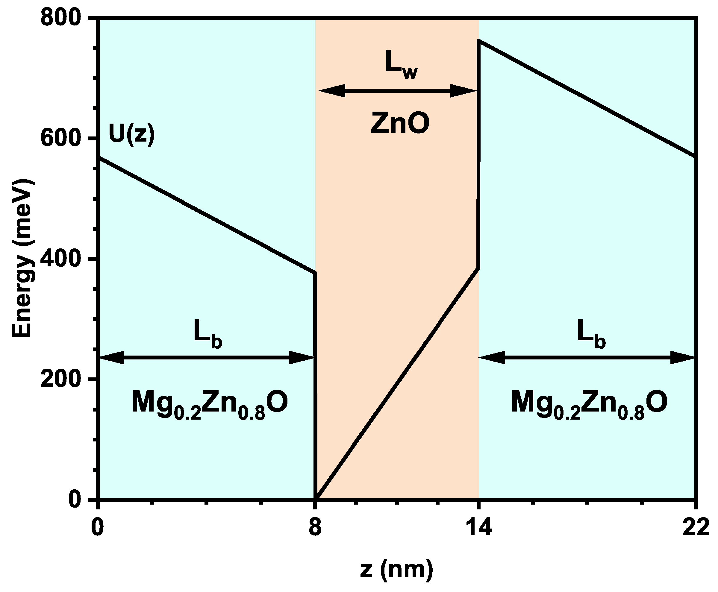
Figure 3.
In (a), variation of the dressed confinement potential V along position on z-axis in a ZnO/O QW system with dimensions for the well and for the barriers. Different values of the dressing parameter are considered. In (b), variation of the energies for ground stated , first and second excited states, and Fermi level (dashed line) depending on the dressing parameter in a ZnO/0 QW system with dimensions and .
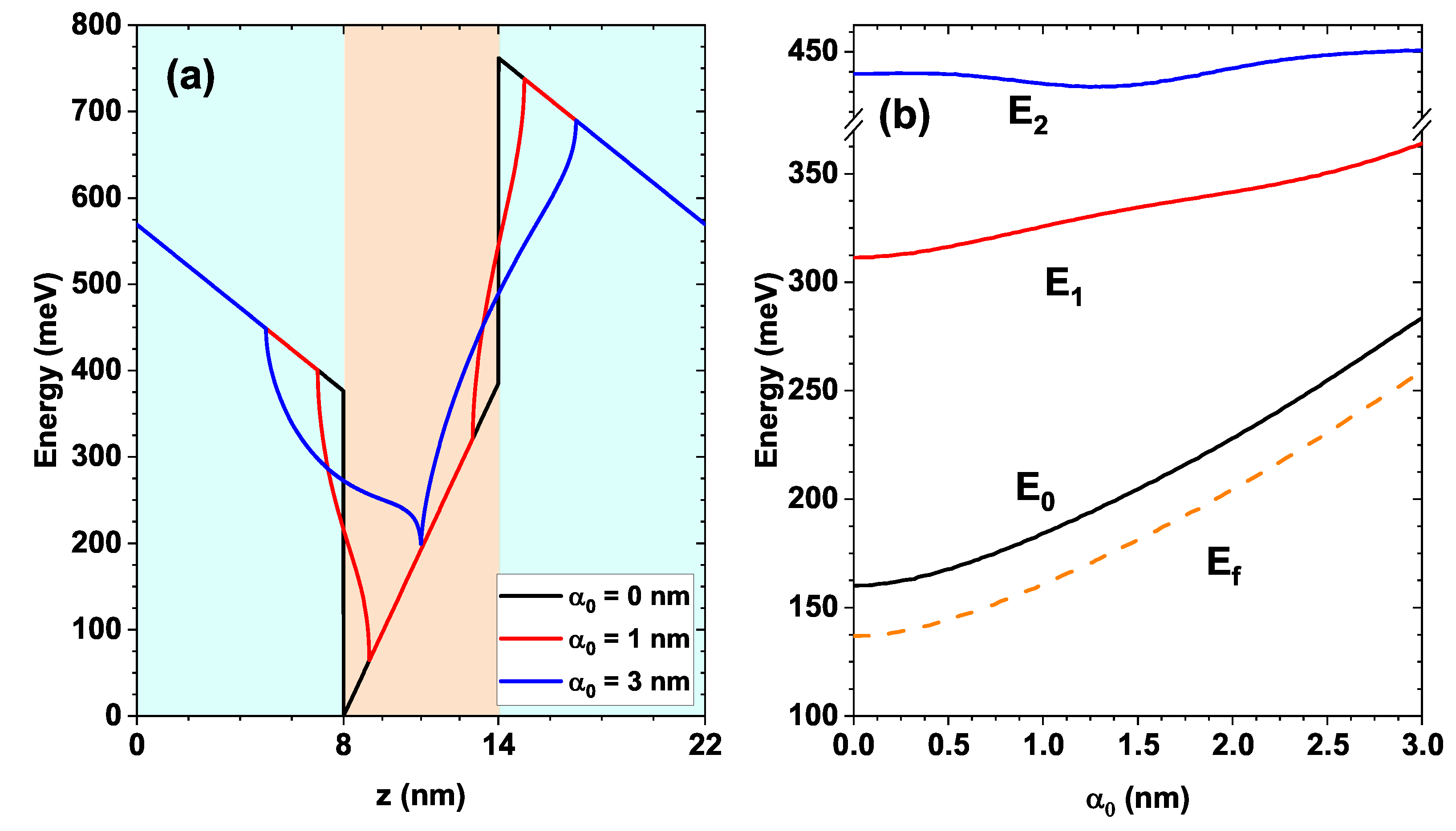
Figure 4.
Normalized wave functions for the first three states for a ZnO/Mg0.2Zn0.8O QW system with dimensions nm and nm, depending upon different values of the dressing parameter . The dashed line represents the point of maximum amplitude for the wave function in each of the values for . In (a), the dressing parameter value taken is nm, while in (b) the parameter is taken as nm. The value in (c) is obtained by the cancellation of the matrix element , which gives nm. In (d), the last value considered for the parameter is nm.
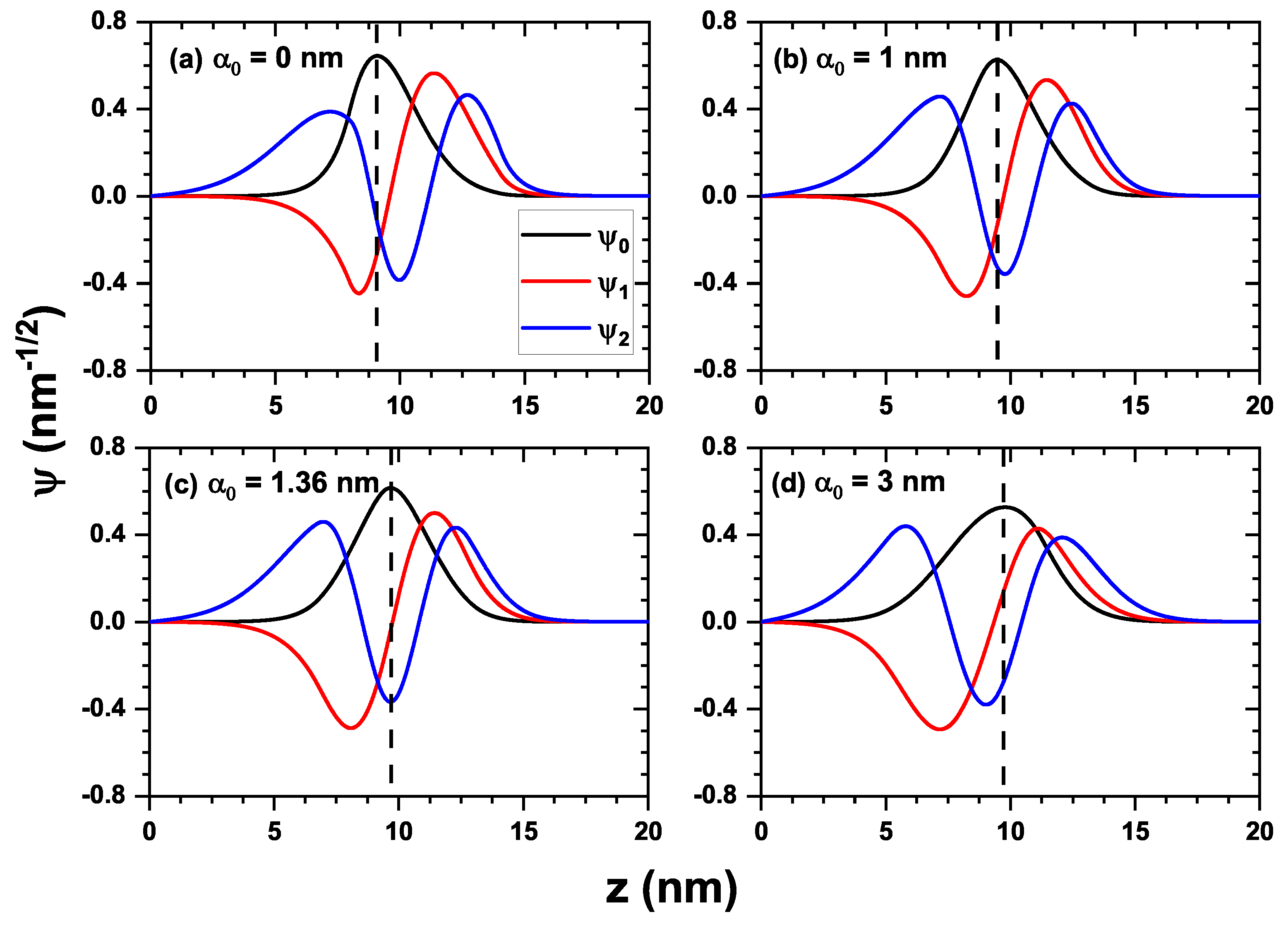
Figure 5.
Argument of the matrix element integral plotted versus position z in the system for a ZnO/Mg0.2Zn0.8O QW system with dimensions nm and nm, considering different values for the dressing parameter . In (a) is depicted the argument for nm, in which the left peak is higher than the right peak. In (b), the peak’s heights are equal for both left and right. In (c) and (d), this characteristic is inverted, since the right peak increases in height while the left peak decreases.
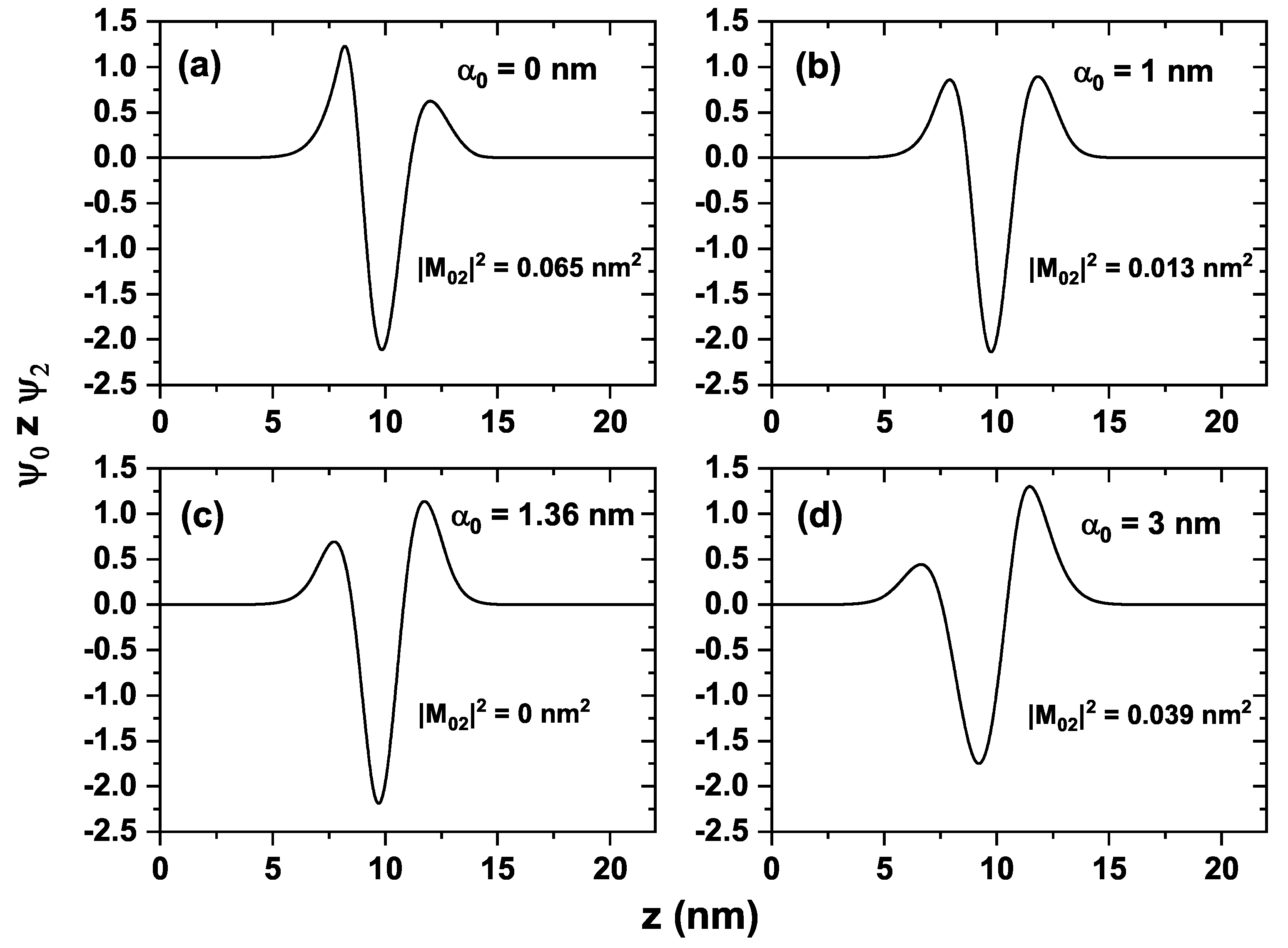
Figure 6.
In (a), absorption coefficient in the given ZnO/O QW system with dimensions nm and nm, depending upon the incident photon’s energy of the resonant laser for different values of . In (b), matrix elements depending on the variation of the dressing parameter for states in the given ZnO/O QW system with dimensions nm and nm. In (c), normalized carrier density per unit area for the states in the given ZnO/O QW system with dimensions nm and nm.
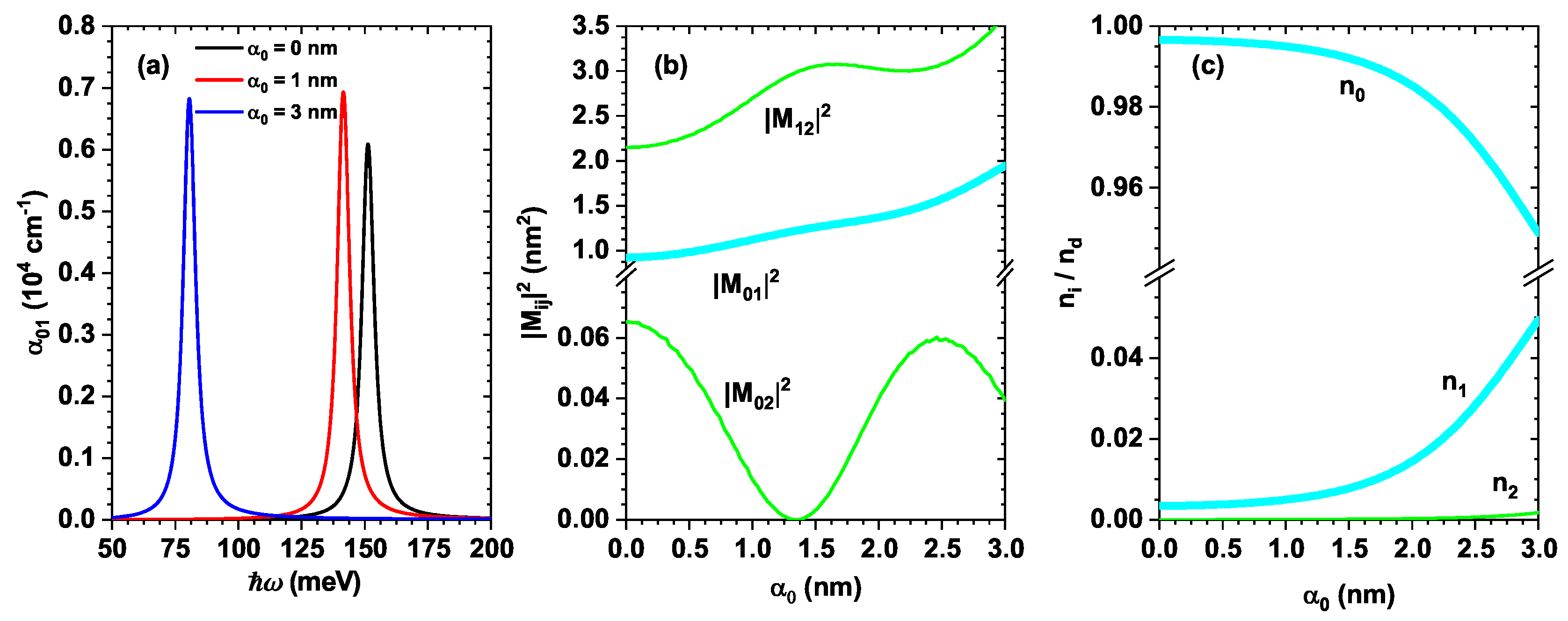
Figure 7.
Raman differential cross section (DCS) in a ZnO/Mg0.2Zn0.8O QW with dimensions nm and nm depending on the emitted radiation energy and different values of the dressing parameter . In (a), the value for the incident laser energy is taken as meV, given by the detuning meV for the Raman transition process to the virtual state. In (b), the energy value for the incident laser is taken as meV for comparison. The picture in (c) shows the second order matrix element depicted as a function of the dressing parameter .
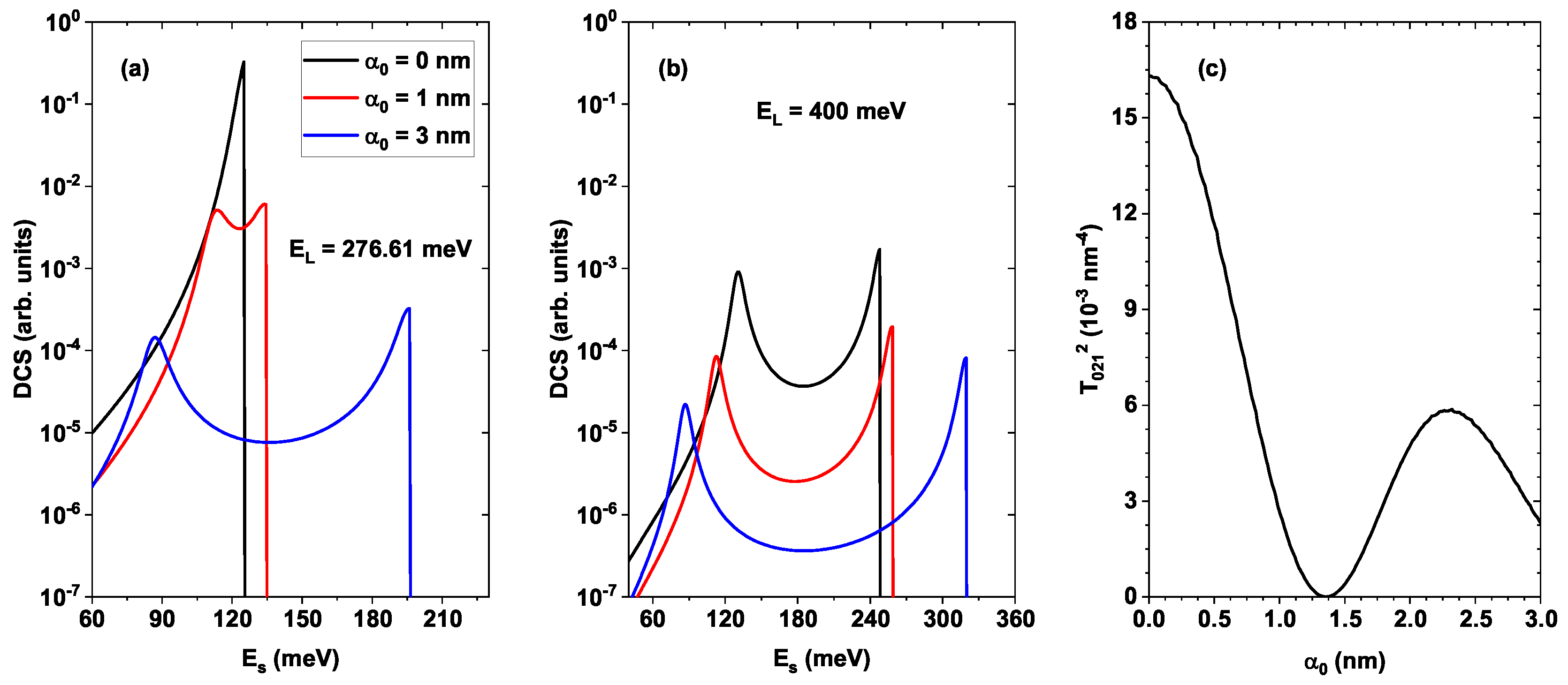
Figure 8.
Raman gain for a electron in the the given ZnO/O QW system whose dimensions are nm and nm as function of the parameter . In (a), the energy for the pumping laser is meV, which is obtained considering the detuning for the Raman transition; here, the gain curve is shown in a thinner range for in which it is seen to have a dominant and well defined peak near nm. In (b), the energy for the pumping laser is taken as meV and the curve, shown for the whole range for is seen to have much less magnitude as in (a) and a very different form.
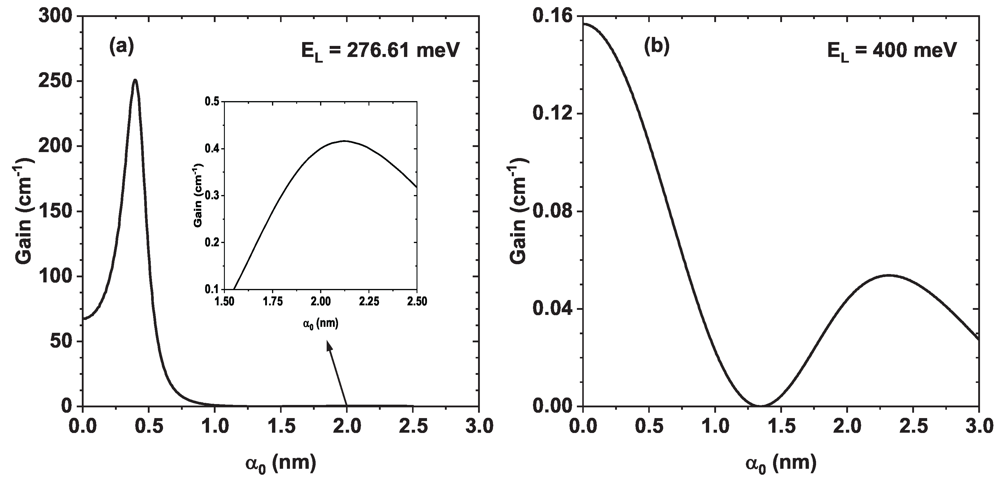

Table 1.
Parameters used for the ZnO/MgxZn1−xO QW calculation.
| Parameter (units) | MgxZn1−xO |
|---|---|
| Vacuum electron mass (kg) | |
| Reduced Planck constant ℏ (eV s) | |
| Boltzmann constant (eV/K) | |
| Vacuum permitivity (F/m) | |
| System temperature T (K) | 300 |
| Well internal electric field (MV/cm) | |
| Barrier internal electric field (MV/cm) | |
| Band discontinuity (meV) | |
| Electron effective mass () [39] | |
| Dielectric constant () [39] | |
| Total polarization (C/m2) [39] | |
| Intrasubband relaxation time (ps) [39] | |
| Incident field’s intensity (W m−2) [39] | |
| Energy bandgap (eV) [43] | |
| Superficial carrier density (cm−2) [44] |
Disclaimer/Publisher’s Note: The statements, opinions and data contained in all publications are solely those of the individual author(s) and contributor(s) and not of MDPI and/or the editor(s). MDPI and/or the editor(s) disclaim responsibility for any injury to people or property resulting from any ideas, methods, instructions or products referred to in the content. |
© 2026 by the authors. Licensee MDPI, Basel, Switzerland. This article is an open access article distributed under the terms and conditions of the Creative Commons Attribution (CC BY) license (http://creativecommons.org/licenses/by/4.0/).
Copyright: This open access article is published under a Creative Commons CC BY 4.0 license, which permit the free download, distribution, and reuse, provided that the author and preprint are cited in any reuse.


