Submitted:
26 January 2026
Posted:
27 January 2026
You are already at the latest version
Abstract
GaN defect quantum emitters constitute a promising platform for single-photon generation in quantum information applications, yet many of their fundamental properties remain poorly understood. In this work, we perform experimental studies of the photoluminescence (PL) polarization of these emitters. Our findings indicate that the PL maintains a high degree of linear polarization across a broad temperature range (10-300 K), with only minor rotations of the polarization axis at intermediate temperatures. We discuss potential physical mechanisms responsible for this behavior and propose directions for future investigations.
Keywords:
GaN
; defcet
; polarization
; quantum emitter
Introduction
For decades, considerable effort has been devoted to the search for ideal single-photon sources to enable a wide range of quantum information technologies[1]. A single-photon source, as the name implies, is a quantum light source capable of emitting individual photons. Unlike classical light sources, it emits at most one photon at any given time, while the probability of emitting two or more photons simultaneously is ideally zero[2]. This property is particularly important for quantum cryptographic communication technologies[3]. An ideal single-photon source should possess at least two fundamental characteristics: high brightness, corresponding to a large photon emission rate, and high stability, enabling reliable operation over extended periods. Beyond these basic requirements, room-temperature operation is highly desirable, as it eliminates the need for complex external cooling systems, such as liquid-helium or liquid-nitrogen cryogenics. Furthermore, compatibility with established material platforms for existing optical components would greatly facilitate integration with mature photonic fabrication technologies.
At the level of basic physical modeling, a single-photon source can be approximated as a two-level system. Research on single-photon sources spans multiple technological approaches. First, it is well known that isolated atoms naturally possess discrete energy levels, from which suitable transitions can, in principle, serve as single-photon emitters. However, the experimental isolation and control of a single atom as a practical single-photon source require highly complex setups, which severely limit its applicability in real-world implementations. Second, quantum-dot-based sources, often regarded as “artificial atoms,” constitute a promising alternative. Through three-dimensional quantum confinement of the host material, the electronic density of states becomes discretized, forming discrete energy levels that enable single-photon emission. In addition, localized defects in wide-bandgap semiconductors often introduce discrete energy levels within the bandgap, enabling them to function as single-photon emitters. Wide-bandgap semiconductors with mature fabrication processes, exemplified by nitride materials, provide an excellent and technologically viable material platform. One major advantage of this platform is that various optical components, such as lasers, LEDs, waveguides, optical cavities, and metasurfaces, can be readily integrated on chip-scale photonic platforms, enabling single-photon emitters to function as on-chip point light sources[4,5,6,7].
We have previously been involved in the development of quantum light sources based on defects in GaN[8,9,10,11,12,13,14]. At present, defect emitters in GaN appear to be particularly promising candidates for single-photon sources. They exhibit high brightness, reaching the megacounts-per-second (Mcps) regime, operate stably at room temperature, and possess narrow emission linewidths[15,16,17]. In addition, the emitted photons are highly linearly polarized[18]. In this work, we present an exploratory study of the polarization properties of GaN defect emitters. Our preliminary experimental results demonstrate that the emitted photons maintain a high degree of linear polarization over a wide temperature range, from cryogenic temperatures to room temperature. However, the polarization orientation exhibits a slight shift, changing from at 10 K to at 300 K, with this minor variation occurring primarily within the intermediate temperature range of 100-200 K. Many questions in this field remain open, and we also summarize and propose potential future research directions and technical approaches.
Results and Discussion
A typical crystal consists of atoms arranged periodically to form a lattice, giving rise to solid-state energy bands, including the conduction band, the bandgap, and the valence band. In a perfect crystal, without defects or boundaries, no energy levels exist within the bandgap. However, any perturbation that disrupts the perfect periodicity of the crystal can modify the band structure. A central question is whether new energy levels are introduced within the bandgap. As schematically illustrated in Figure 1 (a), when a defect, such as a vacancy, an impurity, or a defect complex formed by their combination, is introduced into the crystal, the local lattice periodicity is disrupted. This disruption may give rise to localized defect energy levels within the bandgap. If these energy levels are appropriately positioned, the defect can function as a single-photon source, as shown in Figure 1 (b).
The emission from such defects often exhibits characteristic polarization properties. In general, the eigenstates of a physical system can be classified according to the irreducible representations of its symmetry group, and their degeneracy structure is determined by the dimensionality of these representations. The Hilbert space of eigenstates can be decomposed into a direct sum of irreducible representations, and the selection rules for transitions between energy levels are governed by the tensor product structure of the relevant representations, thereby determining the angular momentum, polarization, and other properties of the emitted photons. More specifically, the polarization characteristics are related both to the symmetry of the underlying crystal structure and to the intrinsic symmetry of the defect itself. Consequently, in the absence of detailed knowledge of the defect, studying the polarization properties of the emitted photons provides a valuable means of inferring its intrinsic characteristics.
Previous studies in GaN have shown that photons emitted from defects are linearly polarized[19]. Furthermore, the polarization orientations predominantly cluster into two groups, around and . This behavior can be understood in terms of the symmetry, with the linearly polarized dipole associated with the defect exhibiting two symmetric lobes, resulting in a periodicity. These observations indicate that the defect cannot be a simple single vacancy or an isolated impurity atom; at a minimum, it must be a complex composed of two or more impurity atoms and/or vacancies. Studying the polarization properties of defect emitters is not only valuable for elucidating their intrinsic nature but also has important implications for practical applications in quantum information. For instance, the classical BB84 quantum key distribution protocol relies on the polarization orientation of individual linearly polarized photons as the computational basis. Although highly attenuated lasers can probabilistically approximate single photons, the emitted photons still follow a coherent-state Poissonian distribution. As illustrated in Figure 1 (c), there remains a finite probability of simultaneously obtaining two or more photons, and extreme attenuation further reduces the number of usable photons. In contrast, a high-brightness single-photon source, such as a GaN defect emitter, offers a natural advantage for quantum key distribution due to its intrinsic single-photon nature and well-defined linear polarization.
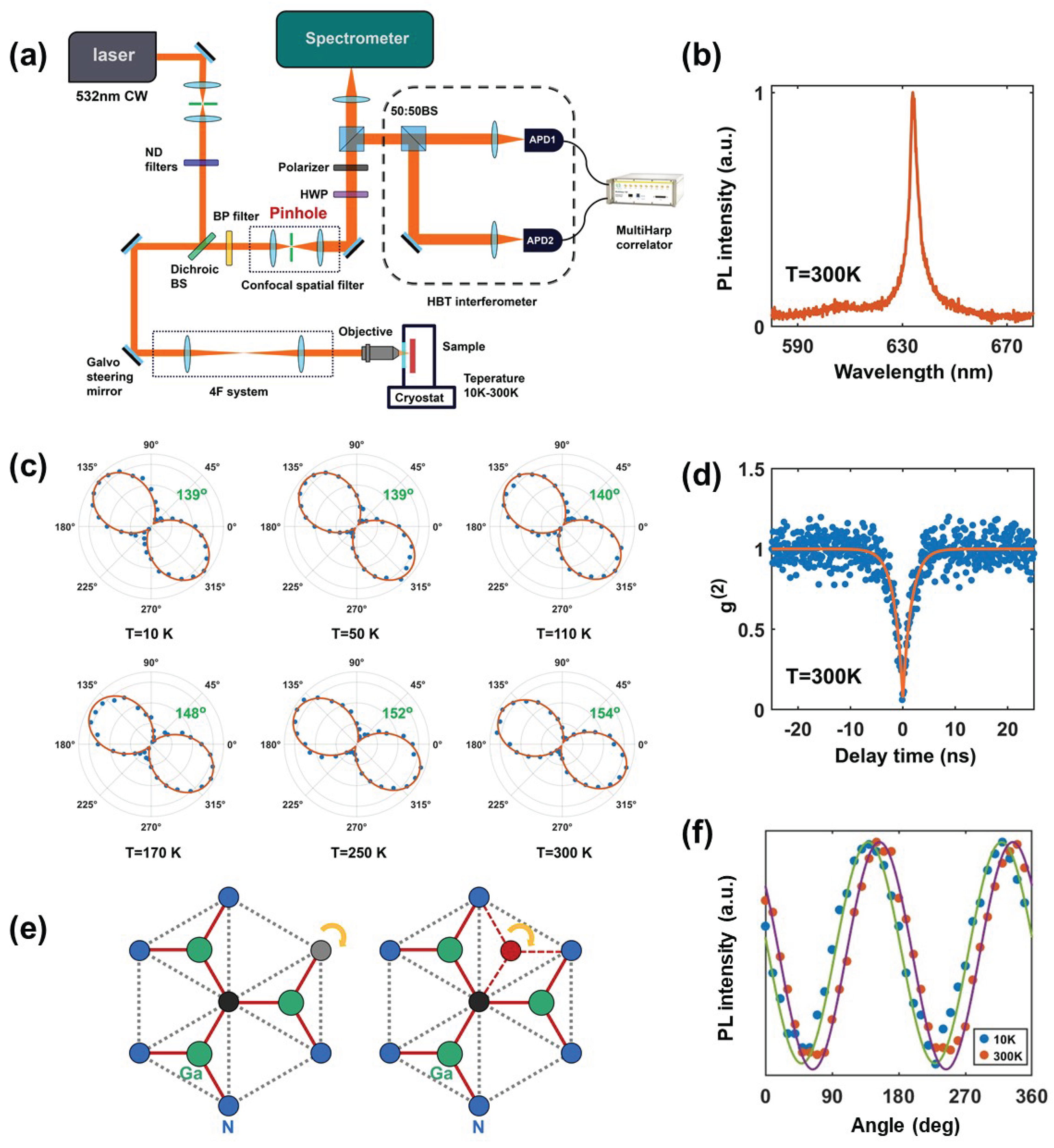
However, prior to studying GaN defect emitters, a significant practical challenge is the efficient collection of photons. Due to the high refractive index of GaN in the visible spectrum (n ∼ 2.4), most of the light emitted by defect emitters undergoes total internal reflection and is redirected back into the substrate. Consequently, only a small fraction of the photons can escape the GaN crystal, not because the defects themselves are insufficiently bright. Several approaches can be employed to address this issue. For example, micro- or nanostructures can be fabricated on the GaN surface, including metasurfaces, Fresnel lenses, or optical waveguides with couplers. Since the emission wavelengths of defect emitters are broadly distributed in the 600-700 nm range, a solid immersion lens (SIL), which is relatively insensitive to wavelength, provides a convenient solution. As illustrated in Figure 1 (d), a hemispherical microlens with a radius of 2.5 m can be fabricated on top of each defect emitter using a focused ion beam. This alters the incident angles of light at the GaN-air interface, mitigating total internal reflection and thereby enabling the extraction of a larger fraction of photons. In general, the performance of a SIL depends on several factors, such as the surface quality, the distance between the defect and the SIL surface, and whether the defect is positioned at the center of the SIL or offset from it. We employ a pre-fabricated point grid, created by FIB etching, as markers to locate each defect, and subsequently align the SIL such that its center coincides with the defect location. As shown in the fluorescence map in Figure 1 (e), the circular dashed line indicates the boundary of the SIL, and the central bright spot corresponds to the defect, which is positioned very close to the SIL center. This protocol achieves a localization error of less than 1 m and generally increases the photon collection efficiency from the defect by approximately a factor of five.
We now turn to the experimental setup and results. Figure 2 (a) illustrates a schematic of the confocal scanning microscope, which serves as the primary tool for studying quantum defects. The key principle is the conjugation between the defect on the sample plane and the pinhole in the collection path, enabling the pinhole to selectively transmit photons from the target defect while rejecting background noise. Scanning mirrors and a 4F system allow the investigation of defects at different positions on the sample. A confocal microscope typically forms the backbone of the setup, with the collection path coupled to various detection modules, most commonly a spectrometer or a Hanbury Brown-Twiss (HBT) interferometer. Variants of this basic framework can be employed to study a wide range of physical properties of quantum defects[2,20]. In the present experiment, a beamsplitter in the collection path enables the simultaneous acquisition of spectral data and second-order correlation measurements. For polarization studies, a rotatable half-wave plate and a fixed polarizer are inserted into the collection path. The sample is mounted in a liquid-helium flow cryostat, allowing the temperature to be tuned from 10 K to 300 K and thereby enabling temperature-dependent experiments[21,22]. Using this setup, we typically obtain results such as those shown in Figure 2 (b)-(d), which are representative of measurements in the field of quantum defects. Figure 2 (b) shows the PL spectrum at room temperature, with a central wavelength of 634 nm in the red spectral range, while Figure 2 (d) presents the corresponding second-order correlation function, demonstrating that the emitter operates as a single-photon source. Figure 2 (c) shows the temperature-dependent polarization data. Strong linear polarization is observed across the entire temperature range from 10 K to 300 K. The polarization orientation, however, gradually shifts from at 10 K to at 300 K. This slight shift occurs primarily within the intermediate temperature range of 100-200 K, while the orientation remains relatively stable at low (<100 K) and high (>250 K) temperatures. For a clearer comparison, the polarization data at 10 K and 300 K, along with fits to a function, are plotted in Figure 2 (f).
Based on the above experimental observations, the polarization properties of defects in GaN are evidently distinct from those of NV centers in diamond. The excited states of NV centers are known to form orbital doublets, giving rise to two mutually orthogonal polarization components ( and )[23]. In contrast, GaN defect emitters do not exhibit such behavior; instead, their excited states are consistent with non-degenerate orbital states with well-defined transition dipoles. This distinction reflects a different underlying symmetry of the defect system, which governs the structure of the electronic states and the associated optical selection rules. Additional insight can be gained from the orientation of the linear polarization. Previous studies have suggested that defects in GaN are unlikely to arise from a single vacancy or impurity atom and are instead expected to consist of complexes formed by two or more vacancies and/or impurities. Nevertheless, the specific spatial configurations of such defect complexes within the GaN lattice remain largely unresolved. If one assumes that entities with the highest wavefunction overlap are the most likely to bind and form a defect complex, the constituent defects are expected to occupy either neighboring lattice sites, substituting for Ga or N atoms, or nearest-neighbor interstitial positions. Under this assumption, several possible defect configurations can be considered, including , , , , and . Here, X and Y denote either impurity atoms or vacancies when occupying lattice sites, while the subscript i indicates an interstitial position.
The specific identities of X and Y, whether impurity atoms or vacancies, remain unknown. Nevertheless, when both X and Y are carbon atoms, the resulting defect complex possesses a dipole moment aligned along the axis connecting the two sites[24]. Carbon incorporation in GaN is known to give rise to the characteristic yellow-band PL emission[25] and is often unavoidable in GaN grown by common crystal growth techniques, such as metal-organic chemical vapor deposition (MOCVD). In addition, other impurity atoms, such as H, O, and Fe, as well as intrinsic Ga or N antisites and vacancies, may also contribute to defect formation. As illustrated in the top-view schematic of the GaN lattice in Figure 2 (e), green and blue dots represent Ga and N atoms, respectively; black and gray dots indicate impurity atoms or vacancies occupying lattice sites, and the red dot denotes an interstitial impurity atom. The presence of a defect locally disrupts the lattice symmetry, altering bond lengths and bond angles relative to the perfect crystal, which in turn induces a deviation of the associated dipole moment. Defects tend to adopt more stable configurations at different temperatures, such as specific bond lengths and bond angles, which can lead to temperature-dependent shifts in the polarization of the emitted photons, as observed in the experimental results shown in Figure 2 (c).
Future experiments on temperature dependent polarization spectroscopy could pursue several directions. One important goal is to examine a large ensemble of defect emitters to obtain statistically meaningful data. Key aspects to investigate include the polarization orientation, any rotation of this orientation, the magnitude of the rotation, and the temperature range over which it occurs, all in relation to the GaN crystal orientation and the defect emitter’s center wavelength. Such systematic measurements would enable a more precise categorization of GaN defect emitters and provide insights into their intrinsic properties. Another promising approach is to perform repeated thermal cycling on individual defect emitters while monitoring the polarization of their PL. In particular, determining whether the polarization rotation occurs reproducibly or randomly would yield critical information about the defect’s atomic configuration and could help distinguish interstitial impurities from substitutional ones.
Clearly, many questions regarding GaN defects remain open, with the most fundamental concerning the nature of the defect itself. Addressing this issue will likely require coordinated efforts from both experimental and theoretical perspectives. Experimentally, it may be necessary to intentionally implant different impurities into the GaN crystal and investigate the resulting defect formation under various conditions, including the type and concentration of the implanted species, as well as annealing temperatures and protocols. By comparing regions before and after implantation, one can verify whether defect emitters have been created in the target areas. From a theoretical perspective, first-principles calculations may be employed to identify defect configurations in GaN that are consistent with the optical properties observed experimentally, thereby providing plausible candidates to guide future experiments.
In general, research in the field of quantum defects follows a structured approach. First, a specific defect in a chosen material system is characterized with respect to its intrinsic physical properties, including PL spectra, energy-level lifetimes, polarization characteristics, and second-order correlation functions, among others. Building on these foundational studies, external stimuli, such as electric or magnetic fields or applied mechanical stress, are then introduced to probe the defect’s response, which often manifests as changes in its PL properties. When the quantum defect also possesses a nontrivial spin, it serves not only as a single-photon emitter but also as a platform for spintronics research, including applications in quantum bits and quantum sensing. Beyond these fundamental studies, quantum defects can serve as quantum light sources in applied engineering contexts, coupled to photonic devices such as cavities and waveguides, thereby forming the basis for integrated photonics research. Additionally, they can be used as quantum bits for quantum computing, analogous to NV center systems, or employed in a range of quantum sensing applications, representing concrete implementations in advanced quantum technologies. This framework is directly applicable to current studies of GaN defect emitters, which largely follow the same research paradigm.
Conclusions
In this work, we present a study of the polarization spectroscopy of GaN defect emitters. Unlike NV centers in diamond, GaN defects exhibit highly pure linear polarization across a wide temperature range (10-300 K), indicating non-degenerate, well-defined orbital excited states with stable transition dipoles, despite a slight temperature-dependent shift in the polarization direction. Possible explanations for this behavior are discussed, and key directions for future research are proposed. These findings are expected to provide useful insights for further studies in the field of quantum defects.
References
- Aharonovich, I.; Englund, D.; Toth, M. Solid-state single-photon emitters. Nature photonics 2016, 10, 631–641. [Google Scholar] [CrossRef]
- Geng, Y. Defect Quantum Emitters in Gallium Nitride. PhD thesis, Cornell University, 2024. [Google Scholar]
- Renner, R. Security of quantum key distribution. International Journal of Quantum Information 2008, 6, 1–127. [Google Scholar] [CrossRef]
- Chen, K.J.; Häberlen, O.; Lidow, A.; lin Tsai, C.; Ueda, T.; Uemoto, Y.; Wu, Y. GaN-on-Si power technology: Devices and applications. IEEE Transactions on Electron Devices 2017, 64, 779–795. [Google Scholar] [CrossRef]
- Yi-Fei, G.; Zhu-Ning, W.; Yao-Guang, M.; Fei, G. Topological surface plasmon. polaritons. Acta Physica Sinica 2019, 68. [Google Scholar] [CrossRef]
- Wasisto, H.S.; Prades, J.D.; Gülink, J.; Waag, A. Beyond solid-state lighting: Miniaturization, hybrid integration, and applications of GaN nano-and micro-LEDs. Applied Physics Reviews 2019, 6. [Google Scholar] [CrossRef]
- Najda, S.P.; Perlin, P.; Suski, T.; Marona, L.; Leszczyński, M.; Wisniewski, P.; Stanczyk, S.; Schiavon, D.; Slight, T.; Watson, M.A.; et al. GaN laser diode technology for visible-light communications. Electronics 2022, 11, 1430. [Google Scholar] [CrossRef]
- Luo, J.; Geng, Y.; Rana, F.; Fuchs, G.D. Room temperature optically detected magnetic resonance of single spins in GaN. Nature Materials 2024, 23, 512–518. [Google Scholar] [CrossRef] [PubMed]
- Luo, J.; Geng, Y.; Farhan, R.; Fuchs, G.; et al. Data and scripts from: Room temperature optically detected magnetic resonance of single spins in GaN. Cornell eCommons, 2024. [Google Scholar]
- Geng, Y. Acoustic Phonon-Induced Dephasing in Gallium Nitride Defect-Based Quantum Emitters. arXiv arXiv:2506.12984.
- Luo, J.; Geng, Y.; Rana, F.; Fuchs, G.D. Room-Temperature Optically Detected Magnetic Resonance of GaN Defect Single-Photon Emitters. In Proceedings of the CLEO: Fundamental Science; Optica Publishing Group, 2023; pp. FM1E–5. [Google Scholar]
- Geng, Y.; Luo, J.; van Deurzen, L.; Jena, D.; Fuchs, G.D.; Rana, F.; et al. Decoherence by Optical Phonons in GaN Defect Single-Photon Emitters. arXiv arXiv:2206.12636.
- Luo, J.; Geng, Y.; Rana, F.; Fuchs, G. GaN quantum emitters: basic physics, spin structure, and optically detected magnetic resonance (ODMR). In Proceedings of the Gallium Nitride Materials and Devices XX. SPIE, 2025; p. PC1336605. [Google Scholar]
- Luo, J.; Geng, Y.; Rana, F.; Fuchs, G. Room temperature optically detected magnetic resonance in single spins hosted in GaN. Bulletin of the American Physical Society, 2024. [Google Scholar]
- Berhane, A.M.; Jeong, K.Y.; Bodrog, Z.; Fiedler, S.; Schröder, T.; Triviño, N.V.; Palacios, T.; Gali, A.; Toth, M.; Englund, D.; et al. Bright Room-Temperature Single-Photon Emission from Defects in Gallium Nitride. Advanced Materials 2017, 29, 1605092. [Google Scholar] [CrossRef] [PubMed]
- Geng, Y.; Luo, J.; van Deurzen, L.; Xing, H.; Jena, D.; Fuchs, G.D.; Rana, F. Dephasing by optical phonons in GaN defect single-photon emitters. Scientific Reports 2023, 13, 8678. [Google Scholar] [CrossRef] [PubMed]
- Geng, Y. Theory of Acoustic-Phonon-Induced Dephasing in GaN Defect Emitters. Preprints, 2026. [Google Scholar]
- Berhane, A.M.; Jeong, K.Y.; Bradac, C.; Walsh, M.; Englund, D.; Toth, M.; Aharonovich, I. Photophysics of GaN single-photon emitters in the visible spectral range. Physical Review B 2018, 97, 165202. [Google Scholar] [CrossRef]
- Geng, Y.; Jena, D.; Fuchs, G.D.; Zipfel, W.R.; Rana, F. Optical dipole structure and orientation of GaN defect single-photon emitters. ACS Photonics 2023, 10, 3723–3729. [Google Scholar] [CrossRef]
- Geng, Y.; Nomoto, K. Ultrafast spectral diffusion of GaN defect single photon emitters. Applied Physics Letters 2023, 123. [Google Scholar] [CrossRef]
- Geng, Y.; Luo, J.; van Deurzen, L.H.; Jena, D.; Fuchs, G.D.; Rana, F. Temperature Dependence of Spectral Emission from GaN Defect Quantum Emitters. In Proceedings of the APS March Meeting 2022, APS, 2022. [Google Scholar]
- Geng, Y. Temperature-Dependent Emission Polarization in GaN Defect-Based Quantum Emitters. arXiv arXiv:2504.18548.
- Fu, K.M.C.; Santori, C.; Barclay, P.E.; Rogers, L.J.; Manson, N.B.; Beausoleil, R.G. Observation of the Dynamic Jahn-Teller Effect in the Excited States of Nitrogen-Vacancy Centers in Diamond. Physical Review Letters 2009, 103, 256404. [Google Scholar] [CrossRef] [PubMed]
- Matsubara, M.; Bellotti, E. A first-principles study of carbon-related energy levels in GaN. II. Complexes formed by carbon and hydrogen, silicon or oxygen. Journal of Applied Physics 2017, 121. [Google Scholar] [CrossRef]
- Lyons, J.; Janotti, A.; Van de Walle, C. Carbon impurities and the yellow luminescence in GaN. Applied Physics Letters 2010, 97. [Google Scholar] [CrossRef]
Figure 1.
(a) Schematic illustration of defect emission in a crystal lattice. Impurity atoms, vacancies, or defect complexes formed by their combination typically emit photons with characteristic polarization. (b) The presence of a defect locally introduces defect levels within the bandgap. If these levels are appropriately positioned, the defect can function as a two-level system and emit single photons. (c) Light from an attenuated laser follows a Poisson distribution, leading to a finite probability of simultaneous multi-photon emission, whereas a true single-photon source emits at most one photon at a time. (d) Each solid immersion lens (SIL) is a hemispherical lens with a radius of 2.5 m. (e) The defect emitter is positioned very close to the center of the SIL.
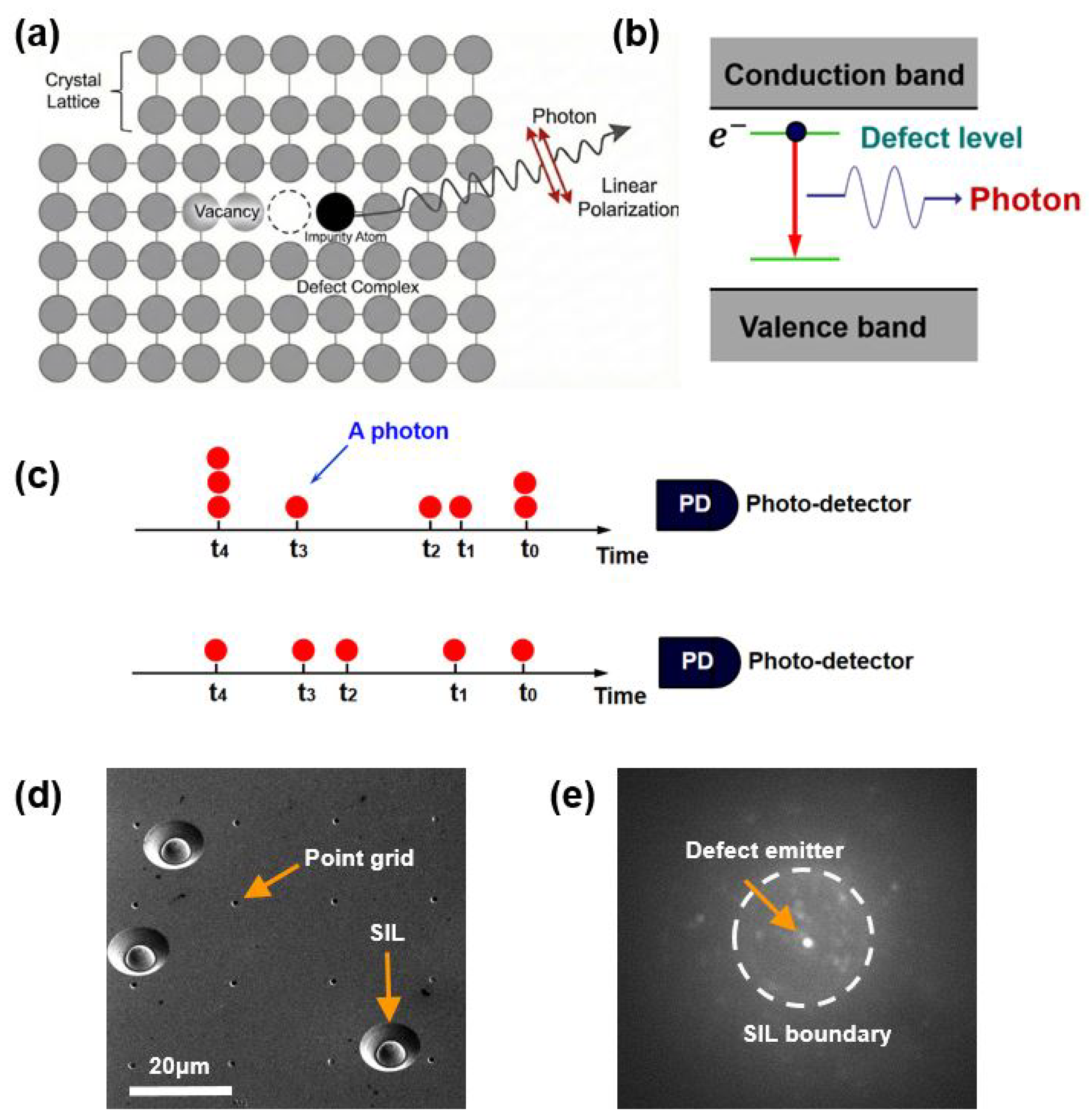
Figure 2.
Experimental results. (a) Schematic of the confocal scanning microscope setup. (b) PL spectrum at room temperature. (c) Temperature-dependent polarization measurements. (d) Second-order correlation function at room temperature. (e) Top view of the GaN crystal lattice. (f) Comparison of polarization data at 10 K and 300 K, along with corresponding fits.
Disclaimer/Publisher’s Note: The statements, opinions and data contained in all publications are solely those of the individual author(s) and contributor(s) and not of MDPI and/or the editor(s). MDPI and/or the editor(s) disclaim responsibility for any injury to people or property resulting from any ideas, methods, instructions or products referred to in the content. |
© 2025 by the author. Licensee MDPI, Basel, Switzerland. This article is an open access article distributed under the terms and conditions of the Creative Commons Attribution (CC BY) license.
Copyright: This open access article is published under a Creative Commons CC BY 4.0 license, which permit the free download, distribution, and reuse, provided that the author and preprint are cited in any reuse.


