Submitted:
23 January 2026
Posted:
26 January 2026
You are already at the latest version
Abstract
The growing need for real-time, accurate monitoring of hazardous gases in environmental, industrial, and healthcare settings has highlighted the limitations of traditional sensing methods. Photonic Integrated Circuits (PICs) have become a revolutionary platform due to their high sensitivity, accurate selectivity, compact size and cost-effectiveness. We present in this work a comprehensive overview of the best-reported PIC-based gas sensors. We discuss the basic concepts behind resonance-based and absorption-based sensing. A detailed overview of the various material platforms, from well-known silicon and silicon nitride to new polymers, chalcogenide glasses, and 2D materials, is presented. A comparison of key device topologies, such as waveguides, microring resonators, Mach-Zehnder interferometers, and metasurfaces, is conducted, with performance benchmarks indicating the limit of detection (LoD). The main limitations of PIC sensors are discussed in this review. We also discuss promising technologies, especially the game-changing potential of artificial intelligence to create fully autonomous devices.
Keywords:
photonic gas sensor
; silicon photonics
; microring Resonator
; Mach‐Zehnder interferometer
1. Introduction
Different applications have different needs when it comes to accurately finding pollutants. Detecting small levels of harmful gases, such as nitrogen dioxide (NO2), carbon monoxide (CO), Sulphur dioxide (SO2), volatile organic compounds (VOCs), and methane (CH4) in parts per billion (ppb), is crucial for maintaining public health and air quality. For industrial safety, on the other hand, the focus is on cost-effectiveness, durability, and the ability to identify harmful or explosive levels, such as finding methane in mines or carbon monoxide in homes. Photonic Integrated Circuits (PICs) are well-positioned to address both of these requirements. They are well-suited for environmental monitoring due to their high sensitivity, and they are also easy to create in large quantities, leading them to be cost-effective for many consumer safety devices [1,2].
Electrochemical and non-dispersive infrared (NDIR) methods have been used for decades to monitor environmental gases [3]. Electrochemical sensors are small, inexpensive, and portable; however, they have several drawbacks, including sensitivity drift, cross-reactivity, and limited lifespan [4]. They work by detecting gases via oxidation reactions at the electrode surface. NDIR devices are more effective at detecting gases like CO2. They consume, however, a significant amount of power, and are typically only sensitive to parts per million (ppm) levels, which is insufficient for real-time trace detection in dynamic or indoor environments [5,6].
To achieve this performance, these sensors exploit nanoscale interactions between light and matter. Photonic Integrated Circuits (PICs) gas sensors can detect gases with high accuracy and high speed by measuring changes in the light signal absorption or shifts in the light resonance wavelength. The complex effective refractive index is measured by the changes in absorption or resonance frequency. Because they use resonance enhancement and nanoscale light confinement, they can detect ppb levels in real time. Nanoscale confinement maximizes the overlap between the optical field and the gas molecules, while resonance structures propagate light, effectively increasing the optical path length and interaction time within a compact footprint [7,8].
Additionally, typical Complementary Metal-Oxide-Semiconductor (CMOS) compatible technology may be used to produce PIC-based sensors. The fabrication of these sensors can be significantly compact and cost-effective. Production is easily scalable by using these methods. Due to their compact size, multiplexed gas detection and integration with electronics or microfluidics are possible. As a result, the development of portable, low-power environmental sensors becomes feasible. Recent research shows that mesoporous-coated Si3N4 Mach-Zehnder interferometers successfully detect volatile organic compounds (VOCs) and NO2 at ppb levels [9,10]. The PIC sector is still growing quickly due to developments in telecommunications and new sensing applications. Such developments are part of a bigger picture of technological change. Market reports indicate that silicon photonics and PIC-based sensor platforms will increase quickly, making them even more popular in real-world applications [11].
Given this potential, the body of literature regarding photonic gas sensing has grown substantially. We looked at more than 150 papers on photonic gas sensing and found 10 review papers that were published between 2020 and 2025. Although these studies examine several aspects of optical sensing, none focus exclusively on integrated gas sensors operating within the visible and near-infrared (VIS–NIR) spectrum.
Butt et al. [12] conducted a thorough review of over 250 articles, and Kazanskiy et al. [13] reviewed over 180 articles to provide general overviews of photonic sensing technologies and their environmental applications. These two reviews covered waveguides and fibres. Tombez et al. [14] focused on methane sensors by reviewing 22 articles. Dinh et al. [3] discussed the non-dispersive infrared (NDIR) technology by reviewing 40 articles. These are two more specific reviews of gas detection. Butt et al. [15] examined integrated sensors by reviewing 159 articles for detecting toxic gases, while Buckley et al. [16] explored the use of graphene and 2D materials for sensing by having a look at 406 articles.
Salama et al. [17] investigated ring resonator-based sensors on silicon platforms’ performance by reviewing 62 articles, while Abood et al. [18] provided a full review of how photonic crystal-based gas sensors were developed by investigating over 160 articles.
Jiang et al. [19] recently contributed to the fundamentals of resonance-based gas sensing when they reviewed 140 articles. Kazanskiy et al. [13] discussed new metasurfaces that make spectroscopy better when exploring 48 articles.
Antonacci et al. [20] did a critical review of the silicon nitride photonics platform for the near-infrared spectrum by reviewing 38 articles. Yang et al. [21] investigated the performance of the lithium niobate platform when it is used for creating an optical waveguide by reviewing 153 articles, while Chowdhury et al. [22] reviewed artificial intelligence applications in gas sensing by investigating 216 articles.
Existing reviews have mostly focused on gas sensing in the mid-infrared (MIR) ‘fingerprint’ region [12] or limited their scope to specific device architectures, such as ring resonators [17]. However, there is a big gap in the literature when it comes to a complete overview of integrated gas sensing in the Visible and Near-Infrared (VIS–NIR) spectrum. Even though there are several studies on this topic, there is still a need to review the performance of Photonic Integrated Circuits (PICs) in the VIS-NIR range. The devices operating in this spectral range have many advantages, such as mature light sources and photodetectors, high yield and low cost due to material abundance and CMOS compatibility in mass production. VIS-NIR gas sensors, however, have lower gas absorption cross-sections than the MIR ones.
This review exclusively examines Integrated Photonic Gas Sensors functioning within the VIS–NIR spectra. We critically analyze the utilization of recent advancements in device engineering (including slot waveguides and metasurfaces) and material hybridization (incorporating polymers, graphene, and two-dimensional materials) to address the decreased absorption sensitivity within this spectrum. This paper connects material science and device topology in a way that previous reviews have not. This review looks at how new platforms like Silicon Nitride, Chalcogenides, and Lithium Niobate have enabled the detection of gases at the part-per-billion (ppb) level in the commercially applicable VIS-NIR spectrum.
This work is structured as follows: we begin in Section 2 with the fundamentals for having a gas sensor and then proceed in Section 3 to material platforms, including silicon, silicon nitride, plasmonic metals, and new hybrids. At the next level in Section 4, we examine the device structures such as microring resonators, Mach-Zehnder interferometers, and waveguides on different material platforms. In Section 5, we address the challenges faced when fabricating these devices and different integration approaches. In addition, we discuss how they might be used in the future in environmental and industrial settings. Finally, the paper ends with the conclusions in Section 6.
2. Fundamentals of Photonic Gas Sensing
Photonic gas sensors utilize the interaction of light with molecules in optical structures to detect the presence of gases and quantify their concentration, as illustrated in Figure 1. This figure is a generic conceptual illustration of how the sensing mechanism works, and it doesn’t depend on any specific material platform or device architecture. It demonstrates the fundamental process in which a light source interacts with gas molecules in a sensing structure, like a resonator, resulting in a detectable change in an output optical signal, such as a change in wavelength, intensity, or phase. These sensors operate on several key principles. Resonance-based detection, used in devices such as microring resonators or photonic crystal cavities, quantifies gas concentration by measuring the refractive-index-induced shift in the resonant wavelength. Absorption-based sensing relies on gas molecules in the evanescent field absorbing light at specific wavelengths, thereby changing the intensity of the transmitted light. A third major category, interferometric sensing, uses devices like Mach-Zehnder interferometers (MZIs) to measure the phase shift induced by gas molecules, which is reflected as a change in the output light intensity [23,24].
2.1. Key Sensing Parameters
To evaluate the effectiveness of photonic gas sensors, it is necessary to measure several key performance metrics. Sensitivity is one of the main metrics. It indicates how much the optical response changes when the medium changes. For sensors that operate based on resonance, this is usually split into gas sensitivity (sgas) and refractometric sensitivity (sn) [17]:
where Δλ is the shift in resonant wavelength, Δn is the change in refractive index resulting from the presence of gas, and ΔC is the change in gas concentration [12,24,25]. The Figure of Merit (FOM) normalizes the sensitivity against the resonance linewidth, which is the Full Width at Half Maximum (FWHM), to consider a spectral resolution [17]:
A higher FOM means that the device can deal with small spectral shifts compared to its linewidth.
Selectivity is another important metric of a gas sensor. It measures the sensor’s ability to distinguish the target gas analyte from other gases that might be present in the medium [26]. The Limit of Detection (LoD) is the lowest gas concentration that can be detected [27]. The response time is another metric which measures the time it takes for the sensor to reach 90% of its output in the presence of the gas [28]. Typical values of the response time range from a few seconds to minutes. For a sensor to function properly in the desired workplace, it is essential to optimize these interdependent parameters.
2.2. Resonance Shift
Resonator-based sensors exploit the refractometric sensitivity of optical modes to small shifts in the effective refractive index of the surrounding medium. The sensor’s sensitivity measures how much the resonant wavelength changes when the refractive index of the surrounding medium is changed [29]. The basic idea underlying the resonance shift is straightforward. A photonic resonator is an optical device carefully designed to trap and circulate light at a specific wavelength, known as its “resonant wavelength” [30]. When gas molecules in the air around the sensor adhere to its surface, they change how light behaves in that area, specifically, the effective refractive index the light experiences. The resonator is consequently ‘detuned’ by this small perturbation, altering its resonant wavelength. Careful measurement of this shift enables quantification of the ambient gas [15].
Highly effective devices have been created using this principle. For instance, a dual-Fano-resonant silicon metasurface operating at about 1.55 µm was developed in [17]. Significant resonance shifts were reported for carbon monoxide (CO). The sensor exhibits a good refractometric sensitivity of 1,735 nm/RIU for CO, along with good figures of merit, demonstrating how tailored resonance shapes can improve gas selectivity and sensitivity [17,31]. Pushing performance further, recent work on suspended nanomembrane silicon (SNS) microring resonators achieved ultra-high intrinsic quality factors by engineering the waveguide to minimize light scattering, which is crucial for detecting minute spectral shifts [32]. In parallel, thermally tunable Ge-on-insulator microring resonators have been demonstrated in the mid-infrared range, enabling dynamic resonance alignment with the strong absorption lines of gases and representing a significant step toward the miniaturization of mid-infrared (MIR) spectrometers [33,34].
2.3. Evanescent-Field-Enhanced Absorption
The evanescent field is the tail of the guided optical mode that goes into the medium surrounding it in absorption-based sensors [35]. Gas molecules in the surrounding medium can absorb light at their unique wavelengths. Optimizing this evanescent-field interaction is essential to how well these photonic gas sensors perform. Recent reviews have emphasized the advantages of complex structures such as slot waveguides and subwavelength-structured (SWG) waveguides, which have been carefully engineered to improve the interaction between light and matter [36]. These designs improve evanescent-field absorption more by strongly confining the light field in the low-index sensing area. Absorption-based sensitivity is thus enhanced by providing more light energy to the area where the gas analyte molecules are, while maintaining acceptable propagation losses [31,37].
The work published in [37] used a slot waveguide to detect methane (CH4). The device demonstrated the power and efficacy of strong optical confinement in the slot geometry, attaining a Limit of Detection (LoD) of 0.3 parts-per-million (ppm). Another study also employed a chalcogenide waveguide to sense acetylene. The design of the waveguide enabled a LoD of roughly 7 ppm [18]. Recent research on chalcogenide hollow-core waveguides [38] has reported a 23 ppm LoD for methane, further supporting this method. A recent theoretical and experimental implementation of a Mach-Zehnder interferometer (MZI) using silicon nitride effectively integrated absorption and sensing [39]. This hybrid method enables simultaneous acquisition of both the real and imaginary parts of the gas analyte’s refractive index, along with a good LoD. These sensing technologies, together, can distinguish between difficult gas combinations more accurately.
2.4. Interferometric and Phase-Based Sensing
Resonators measure shifts in the spectrum, absorption sensors measure loss of intensity, and interferometric sensors measure the phase shift that the gas molecules result in [40]. The Mach-Zehnder Interferometer (MZI) is the most common type of structure for this method. Most MZIs have two paths for the input light: a sensing arm, where the evanescent field is exposed to the gas, and a reference arm, which is protected from outside interference [41].
The principle of operation of interferometric gas sensors is based on the change in the effective refractive index (neff) of the sensing arm that happens when a gas is absorbed. This change causes a phase shift (Δ) in relation to the reference arm. When the signals recombine at the output, this change can be measured as a change in intensity [41]. The phase shift is related to the change in the refractive index using the formula [42]:
where the operating wavelength is, and L is the length of the sensing arm. One of the most beneficial aspects of this method is that sensitivity scales linearly with the sensing length. Researchers use spiral waveguides or folded paths to fit centimeters of optical path length into a small footprint without requiring a larger chip footprint. This approach results in higher sensitivity [43].
Recent progress aimed at reducing the size of these structures while keeping their high sensitivity. For instance, Loop-Terminated MZIs (LT-MZIs) use Sagnac loops to reflect light through the sensing arm, which effectively doubles the interaction length for the same physical footprint [41]. Functionalization is also essential in this field of research. For example, covering the sensing arm with polymers or porous materials like mesoporous silica, graphene oxide [39] allows the gas molecules to stay near the waveguide surface. Therefore, the change in the refractive index is larger. Gases like ammonia (NH3) and volatile organic compounds (VOCs), as a result, could be detected at ppb levels, as shown in recent graphene-oxide optimized fibre MZIs [44].
3. Material Platforms for Integrated Photonic Gas Sensing
In photonic gas sensors, functionalization involves adding specific chemical or nanomaterial layers to the sensor’s surface to enable its interaction with a target gas [39]. This method increases sensitivity and selectivity by encouraging the chosen gas analyte to bind or capture. Capture is the process in which specific gas molecules are selectively trapped on the sensor’s surface, which helps reduce interference from other gases. Advancements in material platforms have primarily driven the evolution of photonic gas sensors over the past few years. These materials dictate critical factors such as optical performance, operational spectral range, fabrication scalability, and compatibility with surface functionality. Interferometers, surface plasmon resonance (SPR) devices, microring resonators, photonic crystals, and metasurfaces are all examples of photonic structures that leverage the unique optical and physical properties of these materials to enable more sensitive, smaller, and more selective devices [45]. The primary materials used in these photonic platforms for gas sensing are reviewed here, with an emphasis on their applications in the visible and near-infrared (NIR) spectral ranges over the past few years.
3.1. Silicon-on-Insulator (SOI)
For a long time, silicon (Si) has been the primary material used in photonic integrated circuits (PICs). It has a high refractive index contrast; its refractive index(n»3.45) is much higher than that of the silicon dioxide substrate (n»1.45) used in SOI wafers [29]. The large refractive index difference provides tight optical confinement, which is an essential feature for small footprints. Coupled with its transparency in the NIR spectrum (especially around 1.3 µm–1.6 µm) and compatibility with current CMOS fabrication methods, these properties render it the best platform. These features allow it to be not only cost-effective and easy to scale, but also ideal for developing high-performance miniaturized gas sensors [31].
Microring resonators developed using SOI have shown excellent sensitivity for gases like nitrogen dioxide (NO2), going below 20 parts-per-billion (ppb), which is an essential level for many environmental monitoring uses [46]. SOI-based MZIs have also been used to detect volatile organic compounds such as ethanol and acetone. They are good for real-time monitoring in healthcare, industrial safety, and indoor air quality assessment [47] because of the fast response time and high sensitivity. SOI is even more appealing because it has low optical loss, is thermally stable, and can handle involved waveguide designs. These advantages enable designers to fabricate both passive and active photonic elements, such as modulators, heaters, and splitters, on the same chip. As a result, fully integrated sensing systems become more useful and effective [48].
Figure 2 demonstrates that there are many ways to produce SOI substrates. For example, a silicon layer could be placed directly on an insulator. Alternatively, a buried oxide (BOX) layer is inserted between the guiding layer and the substrate [49]. Structural flexibility is very important for enabling devices to perform well in specific sensing applications. SOI chips can also be easily connected to optical fibers and support 3D integration. Such integration allows for the development of small, plug-and-play lab-on-chip sensing platforms [50,51,52]. In recent decades, SOI has been very popular in both research and business. As seen in Figure 3 it represents one of the most promising areas for developing new photonic gas sensors, which are precise, fast, small, and easy to use in real life because they are mature, reliable, and work well with existing semiconductor handles [1,2,3].
3.2. Silicon Nitride (Si3N4)
Silicon nitride (Si3N4) is a beneficial material in integrated photonics, especially for applications in the visible to near-infrared (NIR) range. It has a wide transparency range, from visible wavelengths to around 6.7 µm. Consequently, it is great for gas sensing over a wide wavelength range, including shortwave mid-IR (approximately 2–6 µm). That part of the spectrum is particularly valuable because it contains the strong fundamental vibrational absorption lines of many gases. This is often called the molecular fingerprint region, and it provides detection much more sensitive than NIR resonances [10,53]. One of the best characteristics of Si3N4 is that it has very low optical propagation loss across the visible and near-infrared (NIR) spectrum. This high level of transparency is essential when determining trace gas concentrations. That renders it a better and more reliable platform for real-world sensing applications.[54].
The ultra-sensitive refractive-index gas sensor developed with Si3N4 waveguides is a good example [39]. The design of this sensor, built inside a Mach-Zehnder interferometer (MZI), could detect ethanol at about 1.6 parts-per-billion (ppb), acetone at 65 ppb, and isopropyl alcohol at 247 ppb. These limits of detection are the lowest levels yet for PIC-based gas sensors [55]. Recent work on Si3N4 with a common photonic platform demonstrated its appeal, as illustrated in Figure 4. A recent study showed that a silicon nitride platform worked well at 480 nm, 520 nm, and 633 nm with a single-rib waveguide design. Propagation losses were only 3.6 dB/cm, with tight bending radii (~60 µm) and small multi-mode interferometers [53]. The ability to achieve these metrics demonstrates the advanced nature of Si3N4 for covariant visible/NIR photonics.
Si3N4 can support several types of waveguides, including strips, ribs, and slots, as well as various resonator types, including microrings and a Mach-Zehnder interferometer (MZIs). These shapes interact well with thin-film coatings designed to adhere to specific gas molecules. This enables accurate detection of small amounts of gas through evanescent field interactions [57]. Si3N4 has a somewhat lower refractive index contrast than pure silicon, but the trade-off is worth it for applications that need minimal loss, visible-light operation, or are safe for living beings. CMOS methods can be used for manufacturing Si3N4 devices. These devices do not excessively heat, which renders them ideal for use in strong, portable, and mass-producible sensors [58].
3.3. InP and III–V Semiconductors
Indium Phosphide (InP) and related III-V compound semiconductors are crucial for the development of photonic gas sensors, as they address the main challenges of silicon-based platforms. Silicon (Si) and Silicon Nitride (Si3N4) are widely recognized as the premier materials for fabricating passive optical components, offering low propagation losses and high-quality factor resonators [59]. In an indirect bandgap material, the energy maximum of the valence band and the energy minimum of the conduction band are not aligned in momentum space; consequently, for an electron to recombine with a hole and emit a photon, it must simultaneously interact with a phonon (a lattice vibration) to conserve momentum. This inefficient, multi-particle process releases energy primarily as heat rather than light, rendering silicon-based materials unsuitable for active light emission. In contrast, III-V materials possess a direct bandgap where momenta align perfectly, enabling efficient photon emission. This property makes them the industry standard for fabricating the active parts needed to create a complete “spectrometer-on-a-chip,” such as lasers, optical amplifiers, and photodetectors. The main challenge remains how to effectively mount these active III-V components onto passive silicon chips to create a single, compact, and robust sensing device [60].
Recent developments addressed this integration difficulty with two opposing high-performance approaches. The first is monolithic integration, which means growing the III-V material right onto the silicon wafer, as shown in Figure 5. Crystal defects have long plagued monolithic integration. These defects were addressed using the breakthrough InAs Quantum Dot (QD) lasers [61]. The “defect-tolerant” QDs have enabled the construction of monolithic silicon lasers that perform just as well as those on their primary substrate. Such a breakthrough is a big step for high-performance sensors, as it means they can operate at high temperatures (up to 165 °C) without cooling. The monolithic method has already been used for mid-infrared (MIR) sensing. In a recent study, it was reported that Interbrand Cascade Lasers (ICLs) were built on silicon to specifically target methane (CH4) at 3.4 µm [59].
The second technique, heterogeneous integration, involves connecting prefabricated III-V devices to silicon. A significant advancement is a 3D self-aligned flip-chip method that employs electrical surface tension to place two Quantum Cascade Lasers (QCLs) with sub-micron accuracy. Portable MIR spectroscopy at 7.2 µm is thereby enabled, at a size 100 times smaller [62].
The integration method extends beyond light sources to enable the entire sensing system to function. A study [63] shows that InGaAs photodetectors may grow directly on big, 300 mm CMOS-compatible silicon wafers. This approach is essential for NIR sensing (900–1700 nm). It enables the cost-effective, large-scale production of sensors for AI-enhanced analysis and industrial safety [64]. The same “III-V-on-silicon” idea is being used on other materials as well, such as Gallium Nitride (GaN), which enables the development of completely integrated photonic circuits that can sense visible light [65].
3.4. Graphene and 2D Materials
Graphene and other two-dimensional (2D) materials, such as molybdenum disulphide (MoS2) and tungsten disulphide (WS2), are getting a lot of attention as strong tools for using light to sense gases. Because they are so thin, they have a large surface area relative to their volume, so light and matter interact strongly. Because of this property, molecules can stick to surfaces, which can cause visible optical or electrical responses, even when the gas concentrations are very low [16,66]. MoS2 and WS2 are two of the most attractive 2D materials. They are both transition metal dichalcogenides (TMDs). In monolayer conditions, they have direct band gaps that interact with light, altering how light is absorbed. Some studies show that WS2 is better at adsorbing gases such as CO and CO2 than MoS2. Experimental devices have also shown that WS2 responds relatively fast (for example, it takes about 4 to 9 seconds for CO2 ), which renders it a good selection for fast, sensitive environmental monitoring [67].
Graphene exhibits exceptional mechanical strength and high carrier mobility; however, it lacks an intrinsic bandgap. This ‘zero-gap’ characteristic renders its electronic properties highly sensitive to surface perturbations. Upon exposure to gas analytes, molecules adsorb onto the graphene surface and induce charge transfer. These variations in carrier density shift the Fermi level, thereby modulating both the electrical conductivity and the optical absorption. A mixed structure or hybrid composed of graphene and Transition Metal Dichalcogenides (TMDs) takes advantage of graphene’s ability to conduct electricity and the ability of WS2 or MoS2 to absorb light [68,69].
Recent advances in the interaction between light and matter in these 2D materials have improved sensor performance. As illustrated in Figure 6 Combining photonic or nanostructures that contain graphene microcavities, metasurfaces, or metallic resonators significantly amplifies the interaction between the incident light and the adsorbed gas molecules, making this interaction significantly stronger. These engineering changes result in a stronger absorption and a sharper resonance. It additionally provides the ability to find trace-level gases without having to use chemical labels [70,71]. Optimizing layer thickness is essential for real-world gas sensor designs. For example, in surface plasmon resonance (SPR) based designs that use graphene and WS2 on top of a metal layer, the structure’s sensitivity and resonance can change with changes in the number and thickness of the layers. Studies have shown that sensor sensitivity can be higher with graphene/WS2 and metal. Consequently, it is possible to achieve better sensor performance [72].
Chemisorption is the main sensing mechanism for Graphene [74]. Density Functional Theory (DFT) modelling has shown that a large charge transfer between the gas molecule and the graphene sheet causes this process. By adding transition metals like nickel or cobalt to graphene, this interaction can be made selective for certain gases, like CO2 or NO2. The DFT-calculated charge transfer alters the carrier density of graphene, which, in turn, alters its complex refractive index. Integrating functionalized graphene into a PIC, such as an MZI, converts this optical change into a measurable signal. Consequently, a sensor design that works on a chip scale is achieved [75].
3.5. Plasmonic Metals: Surface Plasmon Resonance Platforms
Plasmonic sensors have shown outstanding potential in the last few years for fast, precise detection of gases such as CO, NOₓ, H2, and CO2 [76]. A novel method, localized surface plasmon resonance (LSPR) gas sensitivity, was introduced to measure the extent to which molecular adsorption alters the resonance wavelength, considering the plasmon decay length and surface susceptibility [77]. Figure 7 shows that light-sensitive gas sensors often use noble metals like gold (Au), silver (Ag), and aluminum (Al) because they support SPR and LSPR. These resonances give rise to strong, localized electromagnetic fields at the interfaces between metals and dielectrics. As a result, changes in the refractive index can be detected upon gas adsorption. This framework enables comparisons of different materials and shapes, such as dense arrays of gold nanoparticles that are highly sensitive to a wide range of gases [77].
Recent research investigated multilayer and composite designs to improve performance. Structures such as a patterned LSPR sensor array utilize Au/Ag nanoparticles [79]. They exhibit easy fabrication, multi-gas detection capabilities, and potential applications in environmental and biomedical fields. Nanoporous gold films have also been used for SPR-based gas sensing because they have large surface areas, which enable them to be more easily used for quick and selective detection of CO2 and H2 [80,81].
Tuning the material further enhances gas sensing. Combining silver-based platforms with 2D materials like MoS2 results in stronger electromagnetic confinement and higher refractometric sensitivity [82]. Aluminum-based SPR sensors are less chemically stable, but they have sharper resonances and higher resolution [83]. Current research on hybrid alloys, such as Au–Ag alloys combined with WS2, demonstrates high sensitivities and good figure of merit (FOM), confirming the capability of these nanostructures for the detection of trace gases and biomolecules [84].
3.6. Lithium Niobate (LiNbO3)
Lithium niobate (LiNbO3 or LN) has become one of the most powerful materials in integrated photonics because it has a strong Pockels electro-optic effect [85]. It has a wide range of transparency from ultraviolet to the mid-infrared (MIR) and demonstrates exceptional thermal and mechanical stability. These features allow a fast and easy control of on-chip photonic components, thus explaining the reason why LN is an excellent material for gas sensing applications [86].
Recent studies have utilized LN’s photothermal response for gas detection on a chip, as shown in Figure 8. Integrated LN rib-waveguide sensors have sensitivities that are similar to those of traditional NDIR systems, but they take up a smaller area [87]. The development of high-quality LN thin films generated via economical sputtering, as opposed to ion implantation or smart-cut methods, has increased fabrication challenges while facilitating scalable and low-loss LN photonic devices [21].
Combining LN with Si3N4 in a hybrid way enables the fabrication of wafer-bonded devices. The rationale is that Si3N4 provides low-loss guiding, while LN offers fast electro-optic tuning. LN microring resonators feature real-time voltage-controlled resonance tuning for dynamic gas-absorption matching [88]. Their optical properties additionally render them useful for rapidly interpreting signals and developing small gas sensing devices [86].
3.7. Polymers
Polymers such as polymethylmethacrylate (PMMA) and Sukhoi (SU-8) are becoming increasingly appealing for photonic gas sensing due to their low cost and flexibility. They are also compatible with scalable manufacturing technologies, including spin-coating, hot embossing, and nanoimprinting, as illustrated in Figure 9. PMMA is transparent from visible to near-infrared wavelengths and has a refractive index (n»1.48). SU-8, on the other hand, has a higher refractive index (n»1.57) and can support high-aspect-ratio structuring, which is excellent for patterned sensors and slot waveguides [89,90].
Polymers such as PMMA and benzocyclobutene (BCB) have become desirable platforms because they are flexible and can be used to fabricate large areas at low temperatures. Because they are easy to work with, compact waveguide architectures with integrated functional coatings can be developed. Metal-organic frameworks (MOFs) or polymers, such as polyhexamethylene biguanide (PHMB), significantly enhance gas adsorption and selectivity. Optical gas sensors incorporating MOFs, where sensing is enabled through light interacting with gas molecules inside a thin MOF layer. For example, PMMA ridge waveguides covered in zeolite imidazole framework-8 (ZIF-8) MOFs have been able to detect CO2 in 28 seconds while keeping optical losses low. MOF-coated planar polymer sensors also showed stable, reversible CO2 sensing with fast adsorption, showing that polymers can be both sensitive and reliable in real-world gas-detection applications [91].
Polymer-based waveguides have achieved extraordinary sensitivities through structural innovation and hybrid integration, surpassing those of traditional ridge designs. Bimodal SU-8 waveguides with plasmonic aluminum stripes reached 6300 nm/RIU, while slot-enhanced geometries reached an excellent 2.39 × 10⁵ nm/RIU, which is close to silicon-level performance but at a much lower cost [92,93]. Advanced setups, like slot Bragg grating waveguides filled with functional materials, have shown a good limit of detection (LoD). The implementation of spiral SU-8 waveguides has realized the pioneering on-chip detection of acetylene in the near-infrared (NIR) band [43]. These improvements demonstrate that polymer photonics is a flexible, scalable approach for developing high-performance, small gas sensors with adjustable surface chemistry and enhanced optical confinement.
3.8. Chalcogenide Glasses (As2S3)
Chalcogenide glasses (ChGs), such as arsenic trisulfide (As2S3), are excellent materials for integrated mid-infrared (MIR) photonics because they are highly transparent from the visible range to over 10 µm, including important gas absorption bands. Their high refractive index (n≈ 2.4) and large third-order nonlinearity (n2≈ 2–5 × 10⁻¹⁸ m2/W) enable them to confine light strongly and create efficient nonlinear optical effects in small areas [94]. These characteristics make ChGs ideal for small, label-free on-chip gas-sensing and spectroscopic systems operating in the MIR, where molecular fingerprints are strongest. Recent studies have shown that on-chip As2S3 waveguides can generate a supercontinuum extending deep into the MIR. As a result, they are suitable for multi-gas analysis because they can be used as integrated broadband light sources [95].
Femtosecond laser fabrication has enabled the fabrication of high-quality (Q~106) As2S3 microresonators that can be tuned thermally and optically. These micro resonators can be used as sensitive temperature or refractive index sensors, as shown in Figure 10. Chalcogenide photonic crystal fibers and suspended-core fibers have also generated supercontinua spanning 1.5 to 8 µm. This feature is helpful for fiber-based gas detection because they are transparent in the MIR range and have strong mode confinement [96,97]. These improvements demonstrate the adaptability of ChG materials for both planar and fiber-based sensing systems, and they could even be used in hybrid photonic systems.
Hybrid integration and advanced fabrication techniques continue to improve the performance of ChG photonics by enabling them to work with silicon photonics platforms. Brillouin lasing and two-octave supercontinuum generation are two more examples of how ChG can be used with high-coherence light sources and multi-wavelength gas spectroscopy [98,99]. Also, As2S3 micro resonators are very sensitive, which means they could be used for gas sensing [100]. Chalcogenide-based photonics is a quickly growing field for integrated, broadband, and high-sensitivity gas detection across the MIR spectrum.
4. Photonic Gas Sensor Structures
This section provides an overview of how photonic gas sensors work at their fundamental level. It puts these mechanisms into three main groups. The designs are based on geometric structures that improve light-gas interactions, resonant and filtering structures that detect small changes in light, and interference-based systems that use phase-sensitive measurements. The goal is to highlight how each approach manipulates light to achieve high sensitivity and selectivity for gas detection [50]. Most of these architectures depend on guided light propagation, so the optical waveguide is the most crucial component that holds and directs light, allowing the optical field to interact with the gas analyte surrounding it [101].
A waveguide, like an optical fiber, is a structure formed to direct electromagnetic energy within a specific volume, as shown in Figure 11 [102]. The cross-sectional geometry of the structure plays a crucial role in how light travels through it by determining the supported modes. Each mode represents a transverse field distribution with a specific polarization and amplitude along the direction of propagation [103]. Transverse Electric (TE) and Transverse Magnetic (TM) modes are often used. The difference between them is whether the electric or magnetic field stays perpendicular to the direction of propagation [103,104]. It is important to control these polarization states for sensing. Recent advances, like compact TM-mode filters in rectangular-air-hole 1D photonic crystal waveguides, have shown that this is possible by achieving high polarization extinction ratios. Waveguides can be built in many ways. For example, one-dimensional (1D) photonic crystal waveguides use periodicity to control the flow of light [105]. Two-dimensional (2D) materials like graphene have a layered structure and a large surface-to-volume ratio, which renders them suitable for gas detection [106]. In the end, it is essential to carefully tune the waveguide design, including its cross-section, dimensions, material platform, and modal polarization. Maximizing the overlap between the optical mode and the gas analyte molecules through this tuning improves the sensitivity and performance of photonic gas sensors [103,105].
4.1. Waveguide-Based Photonic Gas Sensors
Photonic gas sensors rely on waveguides to direct light while extending an evanescent field into the surrounding medium, enabling gas molecules to either absorb specific wavelengths or alter the effective refractive index. Various waveguide geometries are discussed, such as rib, slot, and photonic-crystal designs, to enhance this light–matter interaction by increasing field overlap with the gas analyte and improving sensitivity [106]. The following section highlights key advances in photonic waveguide gas sensors across different material platforms, showing how diverse structures are continually optimized for higher performance.
4.1.1. Silicon-Based Platforms (SOI)
A compact CO2 sensor that uses a silicon on insulator (SOI) slotted polymer–phase-shift Bragg grating (SP-PSBG) waveguide integrates polyhexamethylene biguanide (PHMB) directly into a 220 nm-thick slot between silicon rails that are 100 nm separated, as shown in Figure 12. The PHMB-filled slot allows light to interact with the gas analyte, and the 12 nm sidewall corrugations and central defects provide a sharp resonance for accurate detection. The device has a gas sensitivity of 14.4 picometres per part-per-million (pm/ppm), a narrow 1.6 nm full width at half maximum (FWHM), and a figure of merit (FOM) of 9 × 10⁻³ ppm−1, which is better than regular polymer-coated sensors. The 38.2 µm footprint shows how well hybrid silicon–polymer waveguides work for small, high-resolution gas sensing [107].
In addition to these hybrid-polymer methods, designing the shape of the basic silicon waveguide to improve gas sensing remains a significant area of research. A theoretical study examined the fundamental properties of silicon-based ridge waveguides for trace gas detection at a wavelength of 1392 nm [108]. The design was optimized to maximize evanescent-field absorption. By carefully designing the waveguide’s modal dimensions, an evanescent field ratio (EFR) exceeding 30% was achieved, ensuring significant interaction between light and matter. The outcome is high theoretical sensitivity and a good limit of detection (LoD) of 26 ppm.
Experimental work has confirmed this methodology, showcasing on-chip absorption spectroscopy utilizing an extended SOI waveguide. One CH4 sensor used a 10 cm-long silicon waveguide in a small “paperclip” shape to monitor the near-infrared (NIR) absorption line at 1650 nm. The system used the evanescent optical field of the high-index-contrast waveguide to achieve a LoD of less than 100 ppm in the presence of Gaussian noise. This LoD is higher than that of mid-infrared (MIR) alternatives. However, it demonstrates that chip-scale silicon photonics can be utilized for small, cost-effective, and gas monitoring [14].
4.1.2. Silicon Nitride (Si3N4)
The silicon nitride-on-silicon dioxide (SiNOI) platform is suitable for a Mach-Zehnder interferometer (MZI) based sensor across a wide spectral range. A small sensor was developed for use with visible light by using a loop-mirror-terminated (LMT) MZI with a 150 µm slot waveguide sensing arm, as illustrated in Figure 13. The device worked at 650 nm and had a refractometric sensitivity of about 1,320 nm/RIU and a FOM of 641 RIU−1 for this type of setup [109]. The platform is also powerful in the NIR range, where an ultra-sensitive sensor achieved ppb detection using an MZI with long (~5 mm) interference arms and a mesoporous silica functionalization layer. The resultant combination produced an unprecedented LoD of 1.6 ppb for ethanol and 65 ppb for acetone, taking advantage of the Si3N4’s larger evanescent tail, which allowed for stronger light-matter interaction [110]. Resonant waveguide gratings are another type of interferometer. A Si3N4 rib waveguide with a sinusoidally modulated width was used to create a long-period grating (LPG), which showed a high-sensitivity sensor. The structure operates at about 1550 nm, and couples light to modes that strongly affect the medium around them. It has a high refractometric sensitivity of 11,500 nm/RIU, which shows that it could be used for high-performance gas sensing when it is functionalized [111].
4.1.3. Chalcogenide Glass
Chalcogenide glass (ChG) is a key material for gas sensing, and improvements in its fabrication are needed to enhance its performance, as depicted in Figure 14. Adding argon (Ar) to fluorine (CHF3) in an optimized reactive ion-inductively coupled plasma (RIE-ICP) etching process for solid-core GeSbSe waveguides cuts propagation losses in the NIR by a significant amount, bringing them down to 2.6 dB/cm at 1.55 µm [113].
ChG has also been used in a novel manner as the anti-resonant layers in hollow-core structures [38]. These structures trap light in a gas-filled core, resulting in a large external confinement factor (ECF) of about 71%. The following polarization-insensitive design was able to detect acetylene at 1.532 µm and CH4 at 1.654 µm, with a best LoD of 23.07 parts-per-million (ppm).
4.1.4. Lithium Niobate (LiNbO3)
Lithium niobate on insulator (LNOI) is becoming a popular platform for gas sensing because it has strong electro-optic and nonlinear interactions, very low losses (0.34 dB/m at 1550 nm), and high Q-factors (up to 108) [86]. Photothermal (PT) spectroscopy is an advanced sensing technique that uses an LNOI rib waveguide to heat CO2 with a mid-IR pump (2004 nm) and then detect the change in the effective refractive index with a near-infrared (NIR) probe (1550 nm), as shown in Figure 15. The approach has an 870 parts-per-million (ppm) limit of detection (LoD) [87]. Another technique is to use second-harmonic generation (SHG) in a periodically poled (PPLN) waveguide to turn a 1550 nm NIR pump into 775 nm visible light. Gas adsorption alters the phase-matching, shifting the SHG spectrum and giving good sensitivity [114]. LN is great for dynamic sensors because it has a unique combination of electro-optic, piezoelectric, and acousto-optic properties. However, for it to be widely used, high-quality sputtered thin films that can be scaled up are needed to replace wafer-bonded layers [86].
4.1.5. Polymer and Organic Material
Polymers like polymethylmethacrylate (PMMA), Sukhoi (SU-8), and benzocyclobutene (BCB) are becoming more and more popular for photonic gas sensing because they are cheap, flexible, and work well with manufacturing technologies that can be scaled up, as shown in Figure 16 [89,90]. Their ease of processing allows for the integration of functional coatings to improve selectivity, while structural innovations have made polymer waveguides highly sensitive.
By leveraging structural innovation, polymer waveguides have also become highly sensitive. The first on-chip detection of NIR acetylene in the telecom band [43] was enabled by advanced designs, such as a spiral SU-8 waveguide. Also, bimodal SU-8 waveguides have reached refractometric sensitivities of 6300 nm/RIU by using high-confinement geometries, and slot-enhanced geometries have reached an impressive 2.39 × 10⁵ nm/RIU [92,93]. These improvements demonstrate that polymer photonics is a flexible, scalable approach to developing low-cost, high-performance gas sensors.
4.1.6. Graphene and 2D Material Integration
Combining graphene and 2D materials with photonic waveguides enables the creation of a wide range of active and passive gas sensing mechanisms. The creation of an on-chip thermal emitter [117]. It is a big step forward for active components. It uses graphene directly on a silicon waveguide to act as a light source for on-chip spectroscopy, as illustrated in Figure 17. The structure is a step forward towards integrated CO2 detection. 2D materials are also excellent passive sensing layers. For example, a numerical study for a visible and NIR sensor suggested an SPR structure based on a graphene-gold (Au)-silicon carbide (SiC) waveguide. The graphene overlayer in this design enhances molecule adsorption and boosts the evanescent field, thereby greatly increasing the sensor’s predicted sensitivity [118]. The passive method has also been tested in the lab, where a silicon waveguide covered with a few layers of MoS2 was used to find NO2. In this device, the absorption of guided light is changed by the adsorption of NO2 molecules onto the MoS2 surface. Minimal changes can be detected in the waveguide’s output power [119]. These examples demonstrate the flexibility of 2D materials in waveguide-based systems, where they can serve as active emitters or passive layers that enhance absorption or plasmonic-photonic interactions.
4.2. Resonator/Filter-Based Photonic Gas Sensors
Microring resonators and metasurfaces are examples of photonic resonators which confine light. This makes the effective refractive index shift when gas molecules are present. This interaction causes the device’s spectral response to change, as measured, for example, by a change in its resonant wavelength. The high-quality (Q) factor of these structures is an important and essential feature for resonant structures. Narrow resonance linewidths lead to high sensitivity and the detection of very low gas levels [19]. This section discusses major improvements in resonator-based sensors, organized by the primary materials used and the various ways they are used.
4.2.1. Silicon on Insulator
SOI microring resonators (MRRs), as illustrated in Figure 18, are a well-established and effective technology for gas sensing in the near-infrared (NIR) range. They are small, have high Q factors, and are compatible with CMOS technologies. One common way to guarantee that a sensor is selective is to functionalize its surface. Researchers are creating more complex structures to improve the interaction between light and matter, which will ultimately render them more sensitive. For example, a new design combines a slot and a Bragg grating into a “Grating Slot Micro-Ring Resonator” (GSMRR) on the SOI platform. The following is intended for high-efficiency gas sensing in the 1550 nm range [120]. For NIR gas detection, advanced setups with multiple resonators are also under development, such as double-ring resonators (CROWs) [121]. It is possible to design cascaded systems that exploit the Vernier effect [122], which significantly increases overall sensitivity beyond that of a single ring. A study developed a parallel-ring MRR structure to solve the significant issue of cross-sensitivity. The design uses two rings of different widths to simultaneously sense temperature and refractive index, enabling the sensor to distinguish the gas signal from changes in environmental temperature [123].
4.2.2. Silicon Nitride (Si3N4)
Si3N4 is a highly efficient platform for resonator-based sensors because it has low propagation losses, which enable high-Q factors, and broad transparency from the visible (VIS) to the near-infrared (NIR) spectrum [112]. Initial research on Si3N4 race-track resonator-based sensors showed that sensor sensitivity varies with wavelength, as illustrated in Figure 19. A study integrating numerical analysis and experimental validation within the 1520–1600 nm range revealed that the refractometric sensitivity rises from 116.3 nm/RIU to 143.3 nm/RIU at extended wavelengths by using the Si3N4 racetrack resonator structure. It also proved that this design has a good transmission response at different refractive indices, as shown in Figure 20 [112]. Other studies [112] have numerically and experimentally validated that Si3N4 ring resonators for refractive index sensing, attaining comparable sensitivities of approximately 112.5 nm/RIU. One of the main issues with these basic refractometric sensors is their lack of selectivity. They cannot differentiate between gases with similar refractive indices [112]. Functionalization is one of the primary methods to solve this problem. A study [39] showed that coating a Si3N4 photonic resonator with a mesoporous silica layer improved selectivity. This developed a gas sensor with an ultra-high limit of detection (LoD) that could detect ethanol and acetone at levels as low as one part-per-billion (ppb).
4.2.3. Polymer and Organic Materials
All polymer devices are a low-cost and flexible solution for resonator-based sensing. They use properties such as biocompatibility and compatibility with scalable manufacturing methods, including 3D microprinting and inkjet printing [126,127]. For example, a silicon photonic MRR was coated with a polyhexamethylene biguanide (PHMB) polymer layer to create a refractometric sensor for CO2, as illustrated in Figure 21 [128]. This hybrid device had a LoD of 20 parts-per-million (ppm) and excellent transmission response, as shown in Figure 22. The all-polymer whispering-gallery-mode (WGM) microdisk resonator is an excellent example of using Sukhoi (SU-8) polymer to detect volatile organic compounds (VOCs) [126]. These polymers often have a dual-factor sensing mechanism. One factor is the change in the material’s refractive index when it detects gas, and the other is the material’s physical swelling, which changes the resonator’s radius [126]. This dual mechanism is not limited to SU-8. A study [129] of a self-assembled Polydimethylsiloxane (PDMS) micro bottle resonator similarly utilizes both the refractive index and volume change to detect ethanol gas, achieving a high sensitivity of 36.24 in picometres per part-per-million (pm/ppm) [130]. One interesting feature of these platforms is that they use geometric design to improve performance. For example, by creating a larger microdisk undercut, the structure can swell more freely, resulting in a more resonant shift [126]. Another study that used drop-on-demand inkjet printing to create WGM resonators from several polymers (including SU-8, Polystyrene, and PHMB) for detecting gas such as CO2 demonstrated the process’s flexibility [127].
4.2.4. Plasmonic Metasurfaces
Metasurfaces, composed of periodic nanoantennas, are a powerful way to detect gas because they generate strong, localized resonant fields. Functionalization is often used to render these devices more selective. For example, a CO2 sensor created from silicon nano-cylinders on a gold substrate and covered with a very thin layer of the polyhexamethylene biguanide (PHMB) polymer, as illustrated in Figure 23 [13]. When the polymer detects gas, its refractive index changes, which changes the resonance of the metasurface, thus allowing the gas detection with a sensitivity of 17.3 pm/ppm [13].
Plasmonic-based microring resonator structures achieve good results. For example, a plasmonic perfect absorber made from a copper (Cu) grating was shown to support seven different narrowband resonances in the near-infrared (NIR). This multifunctional platform for on-chip gas sensing [131] enjoys a high Q-factor (105) and a refractometric sensitivity of 1991.3 nm/RIU. Recent studies have focused on all-dielectric metasurfaces that enable Fano resonances to achieve sharper responses. A recent study [132] showed that an all-dielectric silicon metasurface working in the NIR has an ultra-high Q-factor and a sensitivity of 2100 nm/RIU. These characteristics render it perfect for finding tiny changes in the refractive index of gas molecules. The metal-insulator-metal (MIM) perfect absorber is another well-known design. Another study [133] suggested a dual-band NIR metasurface sensor utilizing a MIM structure for the detection of volatile organic compounds (VOCs), highlighting its capability for selective, multi-gas analysis through the observation of its unique absorption peaks.
4.3. Interferometer-Based Photonic Gas Sensors
Mach-Zehnder interferometers (MZI) are a primary structure of highly sensitive phase-based gas detection. An MZI works by splitting an incoming beam of light into two paths: a sensing arm that is open to the gas environment and an isolated reference arm. When gas molecules interact with the sensing arm’s evanescent field, the arm’s effective refractive index changes, resulting in a phase shift (Δϕ) relative to the light in the reference arm. When the two beams are put back together, this phase shift changes the interference pattern, resulting in measurable changes in the output power [40]. MZI-based sensing is not only highly sensitive (with a reported limit of detection (LoD) of 1.6 parts-per-billion (ppb) for ethanol), but it is also resistant to common-mode noise from the light source, making it perfect for use in real-world applications [40]. The following subsections discuss significant advances in photonic interferometer gas sensors, grouped by the primary materials used.
4.3.1. Silicon on Insulator
On the mature, CMOS-compatible SOI platform, structural engineering of MZI is key for improving gas-sensing performance in the NIR. One of the most significant challenges is that long sensing arms are needed to achieve high sensitivity, which makes the device larger. The loop-terminated MZI (LT-MZI) is a new concept that uses a Sagnac loop at the end of the arms to reflect light, as illustrated in Figure 24 [41]. The architecture effectively doubles the optical path length for a given physical size, achieving a high figure of merit (FOM) of 280.8 RIU−1 in a compact 150 µm arm length, twice that of a standard MZI, as shown in Figure 25 [41]. The LT-MZI architecture uses a high-interaction slot waveguide for the sensing arm and an isolated strip waveguide for the reference arm. The design principles were successfully tested with a passive oxide-clad device that matched simulations [41]. In a recent study, an asymmetric loop-terminated MZI (a-LT-MZI) based on the idea of combining compact loops with high-interaction waveguides was introduced [134]. It further enhances sensitivity by using a Sagnac loop for compactness and adding an advanced subwavelength grating (SWG) waveguide to the sensing arm. This design improves the interaction between light and matter to give a simulated refractometric sensitivity of 510 nm/RIU [134]. A different way to improve interaction without loops is to change the sensing arm itself. Another study [135] suggested a multi-slot subwavelength grating MZI on the SOI platform. The device combines the strong evanescent field of multiple slots with the dispersion engineering of a SWG structure to create a very sensitive device for sensing refractive index.
4.3.2. Graphene and 2D Materials
2D materials are perfect for fabricating Mach-Zehnder interferometer (MZI) based sensors because they have a very high surface-to-volume ratio [44,136]. Gas molecules stick to the 2D material, which changes its carrier density. These molecules can donate or accept charge, thereby altering the material’s complex refractive index and conductivity. This change causes a measurable phase shift in the MZI [44,136]. An all-fiber MZI is a common type of MZI. It is formed of a tapered thin-core fiber (TCF) spliced between two multimode fibres (MMFs) and covered with a layer of graphene oxide (GO), as shown in Figure 26. It could detect ammonia (NH3) with a linear response and have a high sensitivity, as illustrated in Figure 27 [44]. A strong MZI design created from two 3-dB long-period fiber gratings (LPFGs) covered in graphene was also used to sense ammonia (NH3) [137]. Researchers are looking into hybrid materials that would further enhance sensitivity. A recently developed fibre-based MZI sensor [138] utilized a nanocomposite of gold (Au) nanoparticles and GO as the sensing layer. It was able to detect ammonia at the limit of detection (LoD) of 151 parts-per-million (ppm).
Table 1 shows some of the most significant performance metrics from the research that was covered in this work. This table delivers a clear picture of the state-of-the-art in photonic gas sensing. This comparison shows the characteristics of different approaches by comparing different material platforms (like Silicon-on-Insulator, Silicon Nitride, and polymers) and device architectures (like waveguides, resonators, and interferometers). The table shows the trade-offs and capabilities of each technology by listing the specific target gases and the level of sensitivity that can be achieved. For example, resonator-based systems have high sensitivity, while interferometric designs are more durable.
These performance metrics show how sensitive and flexible current photonic platforms are, but there are still some issues with stability, selectivity, and packaging that need to be worked out before they can be used widely in the real world, which will be discussed in the following section.
5. Challenges and Future Perspectives
Despite the advantages stated previously. There are still several issues that need to be addressed before they can be used to their full potential.
5.1. Challenges and Limitations
It is hard to use photonic gas sensors in real life because they are not selective enough [29]. One of the issues is that other gases could alter the results and trigger false alarms. To be selective, sensors often need to distinguish the target gases from other gases that could be present. Working in the mid-infrared (MIR) range gives a built-in spectroscopic selectivity. Many high-performance near-infrared (NIR) platforms use refractive index sensing, which could respond to other gas analytes and lacks chemical specificity. The widespread use of functional coatings, such as the polyhexamethylene biguanide (PHMB) polymer for CO2 sensing, is driven by the need for chemical specificity. It can be hard to keep these functional layers stable, and they can break down over time [139]. Changes in temperature and humidity may render selectivity much harder because they can change how the sensor reacts to different gases [15].
Another major concern is how hard it is to fabricate the gas sensor. Using CMOS-compatible platforms such as silicon on insulator (SOI) and silicon nitride is a major step toward producing low-cost sensors in large quantities. To develop integrated photonic circuits that can reliably and accurately detect gases, though, advanced manufacturing methods are required. Another problem is how to ensure that the quality and performance are the same for all fabricated devices. It is still a significant engineering challenge to integrate different parts, such as light sources, waveguides, detectors, and gas-sensitive materials, into a single device without sacrificing performance. The packaging of these hybrid systems, which need to have strong electrical, optical, and thermal connections, is often an issue that raises the final cost and makes it harder to have large photonic devices [140,141].
Stability is essential for photonic gas sensors to properly perform over an extended lifetime. One of the issues is that sensor responses change over time. It could happen because the sensor parts wear out, the detector surface becomes contaminated, or the sensors are used in different kinds of weather. Drift makes sensors less accurate and less sensitive [142], requiring recalibration from time to time. Photonic gas sensors can be stabilized with more robust components, coatings, and encapsulation. These measures will help sensors function the same way for a long time and reduce the effects of environmental factors [143].
The limit of detection (LoD) is a significant challenge for photonic gas sensors, as it is difficult to detect small amounts of target gases. It is essential to get low LoDs, especially for safety or environmental monitoring. However, certain factors may limit the LoD of photonic gas sensors. These include noise inherent to the sensor system and interference from background gases. To further improve the LOD, changes to the sensor design may be required. These include selecting appropriate sensing materials, using advanced signal processing to enhance the signal-to-noise ratio, and reducing the sensor sensitivity to gases other than the target one [15,142].
5.2. Future Perspectives
Even with these issues, integrated photonic gas monitors have a bright future. Nanomaterials and metamaterials are two examples of new materials that can improve the performance of sensors. These materials can be rendered more sensitive and selective by having them react with specific gas molecules. Combining photonic sensors with other technologies, such as microelectromechanical systems (MEMS) and microfluidics, may yield small, robust, and real-time monitoring platforms capable of performing many different tasks [18,144].
Advanced computational techniques like adjoint sensitivity analysis (ASA) can produce non-intuitive designs of gas sensors [145]. Through two field simulations, ASA can efficiently calculate the gradient of a Figure of Merit (FOM) with respect to all design parameters, no matter how many there are, using only two simulations [146]. Arfin et al. [147] showed how powerful this method is by making a quad-spectral metasurface router for red, green, blue, and near-infrared (RGB-NIR) sensing. The adjoint-optimized router had an average optical efficiency of about 39% over a wide range (400–850 nm) and a very small footprint of 2 μm × 2 μm, which was much better than regular color filters. Using adjoint-based inverse design methods may accelerate the development of small and powerful photonic gas sensors [148].
A major trend shaping the future of this field is the integration of artificial intelligence (AI) and machine learning (ML). AI is no longer just a way to look at data after it has been collected. It is now a key part of the sensor system itself. By training algorithms on the complex [145], high-dimensional data produced by sensor arrays, also known as “photonic noses” [149], machine learning (ML) can perform advanced pattern recognition to detect and measure multiple gases simultaneously. The cross-sensitivity limits of each sensor element are thereby bypassed. AI can also correct sensor drift and temperature changes in real time, making the system more stable over time. The goal is to achieve “in-sensor computing,” which involves integrating AI algorithms directly into the photonic chip. The outcome will be self-sufficient, smart sensor nodes. [22,150].
Integrated photonics gas sensors could change the way we do things across many fields, such as healthcare, environmental monitoring, and industrial process control. For instance, they could help address environmental and public health problems by providing real-time, on-site air quality monitoring with accuracy never achieved before. These sensors could be used in factories to continuously monitor dangerous gases, providing a safer workplace and more productivity. In healthcare, they could detect biomarkers in a person’s breath, providing a new way to early disease detection without laboratory tests. Another interesting area of research is developing flexible, wearable sensors. These sensors are produced from polymers or 2D materials. They could be used to create personalized environmental monitors that humans can wear. The principles of quantum mechanics may, in the future, enhance sensor performance beyond conventional quantum limits. Using non-classical states of light, such as squeezed light, could reduce photon shot noise and improve the signal-to-noise ratio in experiments. It would render it possible to find things at the very edges of physics [15,151,152].
6. Conclusions
This review studied more than 140 publications focused on integrated photonic gas sensors operating in the visible and near-infrared (VIS–NIR) spectrum. To the best of our knowledge, this is the first review that fully investigates the integration of advanced material science and device engineering within this practical spectral range. We discussed the basic sensing mechanisms, different material platforms (like Silicon-on-Insulator, Silicon Nitride, Chalcogenides, and 2D hybrids), as well as significant architectures like microring resonators and interferometers. Changing from bulk optics to chip-scale Photonic Integrated Circuits (PICs) has made it possible to detect parts-per-billion levels of gas absorption cross-sections, but there are still problems with long-term stability and scalability. Combining these optical detectors with AI and machine learning will greatly improve their performance in the future. The result will lead to smart, self-driving sensors which will render real-time environmental monitoring available to everyone.
References
- Air pollution. Available online: https://www.who.int/health-topics/air-pollution.
- Saxena, P.; Shukla, P. A review on recent developments and advances in environmental gas sensors to monitor toxic gas pollutants. Environmental Progress & Sustainable Energy 2023, vol. 42, e14126. [Google Scholar] [CrossRef]
- Dinh, T.-V.; et al. A Potential Approach to Compensate the Gas Interference for the Analysis of NO by a Non-dispersive Infrared Technique. Anal. Chem. 2020, 92, 12152–12159. [Google Scholar] [CrossRef]
- Gad, S.C.; Handbook, P.D. 2008. [PubMed]
- Xia, L.; Liu, Y.; Chen, R.T.; Weng, B.; Zou, Y. Advancements in miniaturized infrared spectroscopic-based volatile organic compound sensors: A systematic review. Applied Physics Reviews 2024, 11, 031306. [Google Scholar] [CrossRef]
- Kanan, S.; et al. Recent Advances on Metal Oxide Based Sensors for Environmental Gas Pollutants Detection. Critical Reviews in Analytical Chemistry 2025, 55, 911–944. [Google Scholar] [CrossRef] [PubMed]
- Mitchell, C.J.; et al. Mid-infrared silicon photonics: From benchtop to real-world applications. APL Photonics 2024, 9, 080901. [Google Scholar] [CrossRef]
- Molaei-Yeznabad, A.; Shamloo, H.; Abedi, K.; Goharrizi, A.Y. Design and Optimization of a High-Performance CMOS-Compatible Bragg Grating Refractive Index-Based Sensor. Sens Imaging 2024, 25, 70. [Google Scholar] [CrossRef]
- Han, B.; Rupam, T.H.; Chakraborty, A.; Saha, B.B. A comprehensive review on VOCs sensing using different functional materials: Mechanisms, modifications, challenges and opportunities. Renewable and Sustainable Energy Reviews 2024, 196, 114365. [Google Scholar] [CrossRef]
- Yan, Z.; et al. Silicon-Nitride-Integrated Hybrid Optical Fibers: A New Platform for Functional Photonics. Laser & Photonics Reviews 2025, 19, 2400689. [Google Scholar] [CrossRef]
- Siew, S.Y.; et al. Review of Silicon Photonics Technology and Platform Development. J. Lightwave Technol., JLT vol. 39, 4374–4389. Available online: https://opg.optica.org/jlt/abstract.cfm?uri=jlt-39-13-4374. [CrossRef]
- Butt, M.A.; Kazanskiy, N.L.; Khonina, S.N.; Voronkov, G.S.; Grakhova, E.P.; Kutluyarov, R.V. A Review on Photonic Sensing Technologies: Status and Outlook. Biosensors 2023, 13, 568. [Google Scholar] [CrossRef]
- Kazanskiy, N.L.; Butt, M.A.; Khonina, S.N. Carbon Dioxide Gas Sensor Based on Polyhexamethylene Biguanide Polymer Deposited on Silicon Nano-Cylinders Metasurface. Sensors 2021, 21, 378. [Google Scholar] [CrossRef]
- Tombez, L.; Zhang, E.J.; Orcutt, J.S.; Kamlapurkar, S.; Green, W.M.J. Methane absorption spectroscopy on a silicon photonic chip. Optica, OPTICA 2017, 4, 1322–1325. [Google Scholar] [CrossRef]
- Butt, M.A.; Piramidowicz, R. Integrated Photonic Sensors for the Detection of Toxic Gasses—A Review. Chemosensors 2024, vol. 12. [Google Scholar] [CrossRef]
- Buckley, D.J.; Black, N.C.G.; Castanon, E.G.; Melios, C.; Hardman, M.; Kazakova, O. Frontiers of graphene and 2D material-based gas sensors for environmental monitoring. 2D Mater. 2020, 7, 032002. [Google Scholar] [CrossRef]
- Salama, N.A.; Alexeree, S.M.; Obayya, S.S.A.; Swillam, M.A. Silicon-based double fano resonances photonic integrated gas sensor. Sci Rep 2024, 14, 24811. [Google Scholar] [CrossRef] [PubMed]
- Abood, I.; Soliman, S.E.; He, W.; Ouyang, Z. Topological Photonic Crystal Sensors: Fundamental Principles, Recent Advances, and Emerging Applications. Sensors 2025, 25, 1455. [Google Scholar] [CrossRef] [PubMed]
- Jiang, X.; Yang, L. Optothermal dynamics in whispering-gallery microresonators. Light Sci Appl 2020, 9, 24. [Google Scholar] [CrossRef]
- Antonacci, G.; Goyvaerts, J.; Zhao, H.; Baumgartner, B.; Lendl, B.; Baets, R. Ultra-sensitive refractive index gas sensor with functionalized silicon nitride photonic circuits. APL Photonics 2020, 5, 081301. [Google Scholar] [CrossRef]
- Yang, R.; Wei, H.; Tang, G.; Cao, B.; Chen, K. Advanced Crystallization Methods for Thin-Film Lithium Niobate and Its Device Applications. Materials (Basel) 2025, 18, 951. [Google Scholar] [CrossRef]
- Chowdhury, M.A.Z.; Oehlschlaeger, M.A. Artificial Intelligence in Gas Sensing: A Review. ACS Sens. 2025, 10, 1538–1563. [Google Scholar] [CrossRef]
- Khonina, S.; Kazanskiy, N. Environmental Monitoring: A Comprehensive Review on Optical Waveguide and Fiber-Based Sensors. Biosensors 2022, 12, 1038. [Google Scholar] [CrossRef]
- Butt, M.A. Dielectric Waveguide-Based Sensors with Enhanced Evanescent Field: Unveiling the Dynamic Interaction with the Ambient Medium for Biosensing and Gas-Sensing Applications—A Review. Photonics 2024, 11, 198. [Google Scholar] [CrossRef]
- Mishra, V.; Rashmi, R.; Khera, S. Optical Gas Sensors; 2022. [Google Scholar] [CrossRef]
- Wusiman, M.; Taghipour, F. Methods and mechanisms of gas sensor selectivity. Critical Reviews in Solid State and Materials Sciences 2022, 47, 416–435. [Google Scholar] [CrossRef]
- Burgués, J.; Jiménez-Soto, J.M.; Marco, S. Estimation of the limit of detection in semiconductor gas sensors through linearized calibration models. Analytica Chimica Acta 2018, 1013, 13–25. [Google Scholar] [CrossRef]
- Meng, X.; Bi, M.; Xiao, Q.; Gao, W. Ultra-fast response and highly selectivity hydrogen gas sensor based on Pd/SnO2 nanoparticles. International Journal of Hydrogen Energy 2022, 47, 3157–3169. [Google Scholar] [CrossRef]
- Butt, M.A.; Juchniewicz, M.; Słowikowski, M.; Kozłowski, Ł.; Piramidowicz, R. Mid-Infrared Photonic Sensors: Exploring Fundamentals, Advanced Materials, and Cutting-Edge Applications. Sensors (Basel) 2025, 25, 1102. [Google Scholar] [CrossRef]
- Gallego-Martínez, E.E.; Zamarreño, C.R.; Matias, I.R. Resonance-Based Optical Gas Sensors. IEEE Sensors Reviews 2025, 2, 349–375. [Google Scholar] [CrossRef]
- Wu, J.; et al. On-Chip Optical Gas Sensors Based on Group-IV Materials. ACS Photonics 2020, 7, 2923–2940. [Google Scholar] [CrossRef]
- Ranacher, C.; Tortschanoff, A.; Consani, C.; Moridi, M.; Grille, T.; Jakoby, B. Photonic Gas Sensor Using a Silicon Strip Waveguide. Proceedings 2017, 1, 547. [Google Scholar] [CrossRef]
- Lim, J.; Shim, J.; Kim, I.; Kim, S.K.; Geum, D.-M.; Kim, S. Thermally tunable microring resonators based on germanium-on-insulator for mid-infrared spectrometer. APL Photonics 2024, 9, 106109. [Google Scholar] [CrossRef]
- Dong, L.; et al. Versatile Lithium Niobate Platform for Photoacoustic/Thermoelastic Gas Sensing and Photodetection. 2025. [Google Scholar] [CrossRef]
- Butt, M.A. Integrated Photonic Sensors with Enhanced Evanescent Field: Unveiling the Dynamic Interaction with the Ambient Medium. 2024. [Google Scholar] [CrossRef]
- Awasthi, K.; Malviya, N.; Kumar, A. Silicon Subwavelength Grating Slot Waveguide based Optical Sensor for Label Free Detection of Fluoride Ion in Water. IETE Technical Review 2023, 41, 341–352. [Google Scholar] [CrossRef]
- Yallew, H.D.; et al. Sub-ppm Methane Detection with Mid-Infrared Slot Waveguides. ACS Photonics 2023, 10, 4282–4289. [Google Scholar] [CrossRef] [PubMed]
- Min, Y.; et al. On-chip near-infrared multi-gas sensing using chalcogenide anti-resonant hollow-core waveguides. Lab Chip 2025, 25, 1801–1812. [Google Scholar] [CrossRef] [PubMed]
- Antonacci, G.; Goyvaerts, J.; Zhao, H.; Baumgartner, B.; Lendl, B.; Baets, R. Ultra-sensitive refractive index gas sensor with functionalized silicon nitride photonic circuits. arXiv 2020, arXiv:2004.04260arXiv. [Google Scholar] [CrossRef]
- Milvich, J.; Kohler, D.; Freude, W.; Koos, C. Integrated phase-sensitive photonic sensors: a system design tutorial. Adv. Opt. Photon., AOP 2021, 13, 584–642. [Google Scholar] [CrossRef]
- El Shamy, R.S.; Swillam, M.A.; ElRayany, M.M.; Sultan, A.; Li, X. Compact Gas Sensor Using Silicon-on-Insulator Loop-Terminated Mach–Zehnder Interferometer. Photonics 2022, 9, 8. [Google Scholar] [CrossRef]
- Martens, D.; Bienstman, P. Study on the limit of detection in MZI-based biosensor systems. Sci Rep 2019, 9, 5767. [Google Scholar] [CrossRef]
- Zhao, H.; et al. WMS-based near-infrared on-chip acetylene sensor using polymeric SU8 Archimedean spiral waveguide with Euler S-bend. Spectrochimica Acta Part A: Molecular and Biomolecular Spectroscopy 2023, 302, 123020. [Google Scholar] [CrossRef] [PubMed]
- Fan, X.; Deng, S.; Wei, Z.; Wang, F.; Tan, C.; Meng, H. Ammonia Gas Sensor Based on Graphene Oxide-Coated Mach-Zehnder Interferometer with Hybrid Fiber Structure. Sensors 2021, 21, 3886. [Google Scholar] [CrossRef]
- Hodgkinson, J.; Tatam, R.P. Optical gas sensing: a review. Meas. Sci. Technol. 2012, 24, 012004. [Google Scholar] [CrossRef]
- Plößl, A.; Kräuter, G. Silicon-on-insulator: materials aspects and applications. Solid-State Electronics 2000, 44, 775–782. [Google Scholar] [CrossRef]
- Amanti, F.; et al. Integrated photonic passive building blocks on silicon-on-insulator platform. in Photonics, MDPI. 2024, p. 494. Available online: https://www.mdpi.com/2304-6732/11/6/494.
- Shekhar, S.; et al. Roadmapping the next generation of silicon photonics. Nat Commun 2024, 15, 751. [Google Scholar] [CrossRef]
- [49] “Silicon-on-Insulator for Silicon Photonics. Photonics On Crystals. Available online: https://poc.com.sg/silicon-photonics/silicon-on-insulator/.
- Butt, M.A.; Akca, B.I.; Mateos, X. Integrated Photonic Biosensors: Enabling Next-Generation Lab-on-a-Chip Platforms. Nanomaterials 2025, 15, 731. [Google Scholar] [CrossRef] [PubMed]
- Kazanskiy, N.L.; Khonina, S.N.; Butt, M.A. Advancement in Silicon Integrated Photonics Technologies for Sensing Applications in Near-Infrared and Mid-Infrared Region: A Review. Photonics 2022, 9, 331. [Google Scholar] [CrossRef]
- Rudenko, T.E.; Nazarov, A.N.; Lysenko, V.S. The advancement of silicon-on-insulator (SOI) devices and their basic properties. Semiconductor Physics, Quantum Electronics & Optoelectronics 2020, vol. 23. Available online: https://www.researchgate.net/profile/Alexei-Nazarov/publication/344856636_The_advancement_of_silicon-on-insulator_SOI_devices_and_their_basic_properties/links/640a0740bcd7982d8d6e975b/The-advancement-of-silicon-on-insulator-SOI-devices-and-their-basic-properties.pdf.
- Blasco-Solvas, M.; et al. Silicon Nitride Building Blocks in the Visible Range of the Spectrum. J. Lightwave Technol., JLT vol. 42, 6019–6027. Available online: https://opg.optica.org/jlt/abstract.cfm?uri=jlt-42-17-6019. [CrossRef]
- Buzaverov, K.; et al. Silicon Nitride Integrated Photonics from Visible to Mid-Infrared Spectra. Laser & Photonics Reviews 2024, vol. 18. [Google Scholar] [CrossRef]
- Buzaverov, K.A.; et al. Silicon Nitride Integrated Photonics from Visible to Mid-Infrared Spectra. Laser & Photonics Reviews 2024, 18, 2400508. [Google Scholar] [CrossRef]
- Melchiorre, L.; et al. Study and Characterization of Silicon Nitride Optical Waveguide Coupling with a Quartz Tuning Fork for the Development of Integrated Sensing Platforms. Sensors 2025, 25, 3663. [Google Scholar] [CrossRef]
- Corato-Zanarella, M.; Ji, X.; Mohanty, A.; Lipson, M. Absorption and scattering limits of silicon nitride integrated photonics in the visible spectrum. Opt. Express, OE 2024, 32, 5718–5728. [Google Scholar] [CrossRef]
- Bucio, T.D.; et al. Silicon Nitride Photonics for the Near-Infrared. IEEE Journal of Selected Topics in Quantum Electronics 2020, 26, 1–13. [Google Scholar] [CrossRef]
- Díaz-Thomas, D.A.; et al. Single mode, distributed feedback interband cascade lasers grown on Si for gas sensing. Appl. Phys. Lett. 2025, 126, 031102. [Google Scholar] [CrossRef]
- Zeng, C.; Fu, D.; Jin, Y.; Han, Y. Recent Progress in III–V Photodetectors Grown on Silicon. Photonics 2023, 10, 573. [Google Scholar] [CrossRef]
- Papatryfonos, K.; et al. Low-Defect Quantum Dot Lasers Directly Grown on Silicon Exhibiting Low Threshold Current and High Output Power at Elevated Temperatures. Advanced Photonics Research 2025, 6, 2400082. [Google Scholar] [CrossRef]
- Wang, D.; et al. Innovative Integration of Dual Quantum Cascade Lasers on Silicon Photonics Platform. Micromachines 2024, 15, 1055. [Google Scholar] [CrossRef]
- Realising high-performance sensors with heterogeneous integration—Compound Semiconductor News. Compound Semiconductor. Available online: https://compoundsemiconductor.net/article/120720/Realising high-performance sensors with heterogeneous integration—Compound Semiconductor News.
- Shi, B.; Dummer, M.; McGivney, M.; Brunelli, S.S.; Oakley, D.; Klamkin, J. “Heterogeneous Integration of Large-Area InGaAs SWIR Photodetectors on 300 mm CMOS-Compatible Si Substrates”.
- He, H.; et al. Monolithic Integration of GaN-Based Transistors and Micro-LED. Nanomaterials 2024, 14, 511. [Google Scholar] [CrossRef]
- Tao, L.; Chen, Z.; Li, Z.; Wang, J.; Xu, X.; Xu, J.-B. Enhancing light-matter interaction in 2D materials by optical micro/nano architectures for high-performance optoelectronic devices. InfoMat 2021, 3, 36–60. [Google Scholar] [CrossRef]
- Alqaydi, M.; et al. Gas sensing capabilities of MoS2 and WS2: theoretical and experimental study. Emergent Materials 2025. [Google Scholar] [CrossRef]
- Yang, S.; Jiang, C.; Wei, S. Gas sensing in 2D materials. Applied Physics Reviews 2017, 4, 021304. [Google Scholar] [CrossRef]
- Singh, N.J.; Basumatary, I.; Kolli, C.S.R.; Sahatiya, P. Current trends and emerging opportunities for 2D materials in flexible and wearable sensors. Chemical Communications 2025. [Google Scholar] [CrossRef]
- Tsai, H.-S.; Wang, Y.; Liu, C.; Wang, T.; Huo, M. The elemental 2D materials beyond graphene potentially used as hazardous gas sensors for environmental protection. Journal of Hazardous Materials 2022, 423, 127148. [Google Scholar] [CrossRef]
- Wang, D.; Liu, J.; Yang, H.; Huang, B.; Zeng, G. Research on Tunable SPR Sensors Based on WS2 and Graphene Hybrid Nanosheets. Photonics 2022, vol. 9. [Google Scholar] [CrossRef]
- Zhang, L.; Khan, K.; Zou, J.; Zhang, H.; Li, Y. Recent Advances in Emerging 2D Material-Based Gas Sensors: Potential in Disease Diagnosis. Advanced Materials Interfaces 2019, 6, 1901329. [Google Scholar] [CrossRef]
- Gupta, R.K.; et al. Suspended graphene arrays for gas sensing applications. 2D Mater. 2020, 8, 025006. [Google Scholar] [CrossRef]
- Gecim, G.; Ozekmekci, M.; Fellah, M.F. Ga and Ge-doped graphene structures: A DFT study of sensor applications for methanol. Computational and Theoretical Chemistry 2020, 1180, 112828. [Google Scholar] [CrossRef]
- Mollaamin, F.; Monajjemi, M. Transition metal (X = Mn, Fe, Co, Ni, Cu, Zn)-doped graphene as gas sensor for CO2 and NO2 detection: a molecular modeling framework by DFT perspective. J Mol Model 2023, 29, 119. [Google Scholar] [CrossRef]
- Farooq, S.; Bereczki, A.; Habib, M.; Costa, I.; Cardozo, O. High-performance plasmonics nanostructures in gas sensing: a comprehensive review. Med Gas Res 2024, 15, 1–9. [Google Scholar] [CrossRef]
- Proença, M.; et al. New Parameter for Benchmarking Plasmonic Gas Sensors Demonstrated with Densely Packed Au Nanoparticle Layers. ACS Appl Mater Interfaces 2024, 16, 57832–57842. [Google Scholar] [CrossRef]
- Liu, H.; Chen, C.; Zhang, Y.; Bai, B.; Tang, S. A High-Sensitivity Methane Sensor with Localized Surface Plasmon Resonance Behavior in an Improved Hexagonal Gold Nanoring Array. Sensors 2019, 19, 4803. [Google Scholar] [CrossRef]
- Jiang, T.; Guo, H.; Ge, L.; Sassa, F.; Hayashi, K. Inkjet-Printed Localized Surface Plasmon Resonance Subpixel Gas Sensor Array for Enhanced Identification and Visualization of Gas Spatial Distributions from Multiple Odor Sources. Sensors (Basel) 2024, 24, 6731. [Google Scholar] [CrossRef] [PubMed]
- Zhang, C.; Liu, Z.; Cai, C.; Yang, Z.; Qi, Z.-M. Surface plasmon resonance gas sensor with a nanoporous gold film. Opt. Lett., OL 2022, 47, 4155–4158. [Google Scholar] [CrossRef]
- Karki, B.; Trabelsi, Y.; Sarkar, P.; Pal, A.; Uniyal, A. Tuning sensitivity of surface plasmon resonance gas sensor based on multilayer black phosphorous. Mod. Phys. Lett. B 2025, 39, 2450364. [Google Scholar] [CrossRef]
- Sayed, F.A.; Elsayed, H.A.; Mehaney, A.; Aly, A.H. Enhanced Angular Surface Plasmon Resonance Sensor Featuring Ag Nanoparticles Embedded Within a MoS2 Hosting Medium. Plasmonics 2025. [Google Scholar] [CrossRef]
- Proença, M.; et al. New Parameter for Benchmarking Plasmonic Gas Sensors Demonstrated with Densely Packed Au Nanoparticle Layers. ACS Appl Mater Interfaces 2024, 16, 57832–57842. [Google Scholar] [CrossRef]
- Karki, B.; Alsubaie, A.S.; Sarkar, P.; Sharma, M.; Ali, N.B. Detection of Skin, Cervical, and Breast Cancer Using Au–Ag Alloy and WS2-Based Surface Plasmon Resonance Sensor. Plasmonics 2025, 20, 3105–3116. [Google Scholar] [CrossRef]
- Boes, A.; et al. Lithium niobate photonics: Unlocking the electromagnetic spectrum. Science 2023, vol. 379, eabj4396. [Google Scholar] [CrossRef]
- Xie, Z.; et al. Recent development in integrated Lithium niobate photonics. Advances in Physics: X 2024, 9, 2322739. [Google Scholar] [CrossRef]
- Yan, Y.; Feng, H.; Wang, C.; Ren, W. On-chip photothermal gas sensor based on a lithium niobate rib waveguide. Sensors and Actuators B: Chemical 2024, 405, 135392. [Google Scholar] [CrossRef]
- Churaev, M.; et al. A heterogeneously integrated lithium niobate-on-silicon nitride photonic platform. Nat Commun 2023, vol. 14. [Google Scholar] [CrossRef]
- Bhatia, Y.; Zheng, L.; Steinbach, L.; Günther, A.; Schneider, A.; Roth, B. Low-cost scalable fabrication of functionalized optical waveguide arrays for gas sensing application. Int J Adv Manuf Technol 2025, 138, 617–633. [Google Scholar] [CrossRef]
- Prasanna Kumaar, S.; Sivasubramanian, A. Analysis of BCB and SU 8 photonic waveguide in MZI architecture for point-of-care devices. Sensors International 2023, 4, 100207. [Google Scholar] [CrossRef]
- Zheng, L.; Keppler, N.; Zhang, H.; Behrens, P.; Roth, B. Planar Polymer Optical Waveguide with Metal-Organic Framework Coating for Carbon Dioxide Sensing. Advanced Materials Technologies 2022, vol. 7. [Google Scholar] [CrossRef]
- Bhalerao, O.; et al. High-sensitivity polymer-based bimodal plasmonic refractive index sensors with polymer cladding. Optics Express 2025, 33, 9813–9824. Available online: https://opg.optica.org/abstract.cfm?uri=oe-33-5-9813. [CrossRef]
- Kumaar, S.P.; Sivasubramanian, A. Analysis of BCB and SU 8 photonic waveguide in MZI architecture for point-of-care devices. Sensors International 2023, 4, 100207. [Google Scholar] [CrossRef]
- Kobayashi, H.; Kanbara, H.; Koga, M.; Kubodera, K. Third-order nonlinear optical properties of As2S3 chalcogenide glass. J. Appl. Phys. 1993, 74, 3683–3687. [Google Scholar] [CrossRef]
- Xia, K.; et al. Supercontinuum generation in As2S3 chalcogenide waveguide pumped by all-fiber structured dual-femtosecond solitons. Optics Express 2023, 31, 29440–29451. [Google Scholar] [CrossRef]
- Van, B.C.; Tran, B.T.L.; Van, L.C. Mid-infrared supercontinuum generation in As2S3-circular photonic crystal fibers pumped by 4.5 µm and 6 µm femtosecond lasers. J. Opt. Soc. Am. B, JOSAB 2024, 41, E1–E7. [Google Scholar] [CrossRef]
- Zhang, B.; Xia, D.; Zhao, X.; Wan, L.; Li, Z. Hybrid-integrated chalcogenide photonics. gxjzz 2023, 4, 503–518. [Google Scholar] [CrossRef]
- Shanavas, T.; Grayson, M.; Xu, B.; Zohrabi, M.; Park, W.; Gopinath, J.T. Cascaded forward Brillouin lasing in a chalcogenide whispering gallery mode microresonator. APL Photonics 2022, vol. 7. [Google Scholar] [CrossRef]
- Zhao, P.; Yang, L.; Xia, K.; Yang, P.; Wang, R.P.; Xu, P. Exceeding two octave-spanning supercontinuum generation in integrated As2S3 waveguides pumped by a 2 μm fiber laser. Optics & Laser Technology 2024, 177, 111065. [Google Scholar] [CrossRef]
- Andrianov, A.V.; Marisova, M.P.; Anashkina, E.A. Thermo-Optical Sensitivity of Whispering Gallery Modes in As2S3 Chalcogenide Glass Microresonators. Sensors 2022, 22, 4636. [Google Scholar] [CrossRef] [PubMed]
- Ramola, A.; Shakya, A.K.; Kumar, V.; Bergman, A. Recent Advances in Photonic Crystal Fiber-Based SPR Biosensors: Design Strategies, Plasmonic Materials, and Applications. Micromachines (Basel) 2025, 16, 747. [Google Scholar] [CrossRef]
- Available, A.O. 360042305154-Waveguide-FEEM.
- Gemo, E. The design and analysis of novel integrated phase-change photonic memory and computing devices. 2021. [Google Scholar] [CrossRef]
- 6 meanings of Te and TM in rectangular waveguide. DOLPH MICROWAVE. Available online: https://www.dolphmicrowave.com/default/6-meanings-of-te-and-tm-in-rectangular-waveguide/.
- Kazanskiy, N.L.; Butt, M.A.; Khonina, S.N. 2D-Heterostructure Photonic Crystal Formation for On-Chip Polarization Division Multiplexing. Photonics 2021, vol. 8. [Google Scholar] [CrossRef]
- Ma, N.; et al. Design of On-Chip Multi-Slot Chalcogenide Waveguide for Mid-Infrared Methane Sensing. Microwave and Optical Technology Letters 2024, vol. 66, e70036. [Google Scholar] [CrossRef]
- Khafagy, M.; Khafagy, M.; Hesham, P.; Swillam, M.A. On-Chip Silicon Bragg-Grating-Waveguide-Based Polymer Slot for Gas Sensing. Photonics 2025, vol. 12. [Google Scholar] [CrossRef]
- Faghihi, V.; Goodarzi, R. Silicon ridge waveguide for trace gas detection. Thin films 2025. [Google Scholar]
- Sultan, A.; Sabry, Y.M.; Samir, A.; El-Aasser, M.A. Mirror-terminated Mach-Zehnder interferometer based on SiNOI slot and strip waveguides for sensing applications using visible light. Front. Nanotechnol. 2023, vol. 5. [Google Scholar] [CrossRef]
- Antonacci, G.; Goyvaerts, J.; Zhao, H.; Baumgartner, B.; Lendl, B.; Baets, R. Ultra-sensitive refractive index gas sensor with functionalized silicon nitride photonic circuits. APL photonics 2020, vol. 5. Available online: https://pubs.aip.org/aip/app/article/5/8/081301/123341. [CrossRef]
- Deleau, C.; Seat, H.C.; Bernal, O.; Surre, F. High-sensitivity integrated SiN rib-waveguide long period grating refractometer. Photon. Res., PRJ 2022, 10, 564–573. [Google Scholar] [CrossRef]
- Butt, M.A.; et al. Investigation of Modal Characteristics of Silicon Nitride Ridge Waveguides for Enhanced Refractive Index Sensing. Micromachines 2025, 16, 119. [Google Scholar] [CrossRef]
- Hammouti, A.; et al. Etching parameter optimization of photonic integrated waveguides based on chalcogenide glasses for near- and mid-infrared applications. Opt. Mater. Express, OME 2025, 15, 775–787. [Google Scholar] [CrossRef]
- Rao, A.; et al. Second-harmonic generation in periodically-poled thin film lithium niobate wafer-bonded on silicon. Opt. Express, OE 2016, 24, 29941–29947. [Google Scholar] [CrossRef]
- Jia, J.; et al. Mid-Infrared Highly Efficient, Broadband, and Flattened Dispersive Wave Generation via Dual-Coupled Thin-Film Lithium-Niobate-on-Insulator Waveguide. Applied Sciences 2022, vol. 12. [Google Scholar] [CrossRef]
- Ji, L.; Yang, S.; Shi, R.; Fu, Y.; Su, J.; Wu, C. Polymer Waveguide Coupled Surface Plasmon Refractive Index Sensor: A Theoretical Study. Photonic Sens 2020, 10, 353–363. [Google Scholar] [CrossRef]
- Negm, N.; et al. Graphene Thermal Infrared Emitters Integrated into Silicon Photonic Waveguides. ACS Photonics 2024, 11, 2961–2969. [Google Scholar] [CrossRef] [PubMed]
- Du, W.; Miller, L.; Zhao, F. Numerical Study of Graphene/Au/SiC Waveguide-Based Surface Plasmon Resonance Sensor. Biosensors 2021, 11, 455. [Google Scholar] [CrossRef]
- Li, W.; Shahbazi, M.; Xing, K.; Tesfamichael, T.; Motta, N.; Qi, D.-C. Highly Sensitive NO2 Gas Sensors Based on MoS2@MoO3 Magnetic Heterostructure. Nanomaterials 2022, 12, 1303. [Google Scholar] [CrossRef]
- Valdiviezo, J.H.M.; Torchia, G.A. Design and development of integrated sensors under the silicon on insulator (SOI) platform for applications in the near/mid-infrared (NIR/MIR) band. in Nanoengineering: Fabrication, Properties, Optics, Thin Films, and Devices XXI, SPIE, Oct. 2024, pp. 77–90. [CrossRef]
- Valdiviezo, J.H.M.; Torchia, G.A. Design and development of integrated sensors under the silicon on insulator (SOI) platform for applications in the near/mid-infrared (NIR/MIR) band. In Nanoengineering: Fabrication, Properties, Optics, Thin Films, and Devices XXI; SPIE, 2024; pp. 77–90. [Google Scholar] [CrossRef]
- He, M.; Zhu, B.; Zhang, Z. High Sensitivity Temperature Sensor Based on Harmonic Vernier Effect. Photonic Sens 2023, 13, 230204. [Google Scholar] [CrossRef]
- Zheng, S.; Jiang, X.; Jiang, D. SOI-based parallel-ring microresonator for simultaneous sensing of refractive index and temperature. Appl. Opt., AO 2025, 64, 535–542. [Google Scholar] [CrossRef] [PubMed]
- Uchida, Y.; Arakawa, T.; Higo, A.; Ishizaka, Y. Silicon Microring Resonator Biosensor for Detection of Nucleocapsid Protein of SARS-CoV-2. Sensors 2024, 24, 3250. [Google Scholar] [CrossRef]
- Kar, S.; Singhal, S.; Paithankar, P.; Varshney, S.K. Microring Resonators and its Applications. Indian Journal of Pure & Applied Physics (IJPAP) 2023, 61, 601–621. [Google Scholar] [CrossRef]
- Lemieux-Leduc, C.; Guertin, R.; Bianki, M.-A.; Peter, Y.-A. All-polymer whispering gallery mode resonators for gas sensing. Optics express 2021, 29, 8685–8697. Available online: https://opg.optica.org/abstract.cfm?uri=oe-29-6-8685. [CrossRef]
- Bianki, M.-A.; Guertin, R.; Lemieux-Leduc, C.; Peter, Y.-A. Suspended whispering gallery mode resonators made of different polymers and fabricated using drop-on-demand inkjet printing for gas sensing applications. Sensors and Actuators B: Chemical 2024, 420, 136460. [Google Scholar] [CrossRef]
- Wang, J.; et al. A Silicon Microring Resonator for Refractive Index Carbon Dioxide Gas Sensing. ACS Sens. 2025, 10, 4938–4944. [Google Scholar] [CrossRef]
- Zhu, N.; Shi, B.; Guo, Y.; Han, B.; Zhang, Y. Polydimethylsiloxane self-assembled whispering gallery mode microbottle resonator for ethanol sensing. Optical Materials 2020, 107, 110024. [Google Scholar] [CrossRef]
- Mazuryk, J.; Paszke, P.; Pawlak, D.A.; Kutner, W.; Sharma, P.S. Fabrication, Characterization, and Sensor Applications of Polymer-Based Whispering Gallery Mode Microresonators. ACS Sens. 2025, 10, 5314–5338. [Google Scholar] [CrossRef]
- Mohamed, Z.A.; Almawgani, A.H.M.; Gumaih, H.S.; Adam, Y.S. Plasmonic Multi-resonator Perfect Absorber with Narrowband Modes for Optical Sensing. Plasmonics 2025. [Google Scholar] [CrossRef]
- Salama, N.A.; Obayya, S.S.A.; Alexeree, S.M.; Swillam, M.A. Ultra-sensitive gas sensor using Fano resonance in hybrid nano-bar/nano-elliptic dielectric metasurface. in Metamaterials XIV, SPIE, Jun. 2023, pp. 113–117. [CrossRef]
- Wang, L.; et al. Multi-Band Terahertz Metamaterial Absorber Integrated with Microfluidics and Its Potential Application in Volatile Organic Compound Sensing. Electronics 2025, 14, 2731. [Google Scholar] [CrossRef]
- Butt, M.A. High Sensitivity Design for Silicon-On-Insulator-Based Asymmetric Loop-Terminated Mach–Zehnder Interferometer. Materials 2025, 18, 798. [Google Scholar] [CrossRef] [PubMed]
- Guo, Y.; Yan, B.; Qi, Y. SOI optical waveguide-based refractive index sensor using a multi-slot subwavelength grating Mach–Zehnder interferometer. Appl. Opt., AO 2025, 64, 5896–5902. [Google Scholar] [CrossRef] [PubMed]
- Wang, J.; Xing, Z.; Chen, X.; Cheng, Z.; Li, X.; Liu, T. Recent Progress in Waveguide-Integrated Graphene Photonic Devices for Sensing and Communication Applications. Front. Phys. 2020, vol. 8. [Google Scholar] [CrossRef]
- Hao, T.; Chiang, K.S. Graphene-Based Ammonia-Gas Sensor Using In-Fiber Mach-Zehnder Interferometer. IEEE Photonics Technology Letters 2017, 29, 2035–2038. [Google Scholar] [CrossRef]
- Fenjan, D.; Mahdi, B.; Yusr, H. Graphene Oxide-Coated Mach-Zehnder Interferometer Based Ammonia Gas Sensor. Nexo Revista Científica 2023, 36, 1132–1140. [Google Scholar] [CrossRef]
- Elrashidi, A.; Traversa, E.; Elzein, B. Highly sensitive ultra-thin optical CO2 gas sensors using nanowall honeycomb structure and plasmonic nanoparticles. Front. Energy Res. 2022, vol. 10. [Google Scholar] [CrossRef]
- Illuminating the Future: The Promise and Challenges of Photonics | Synopsys Optical and Photonic Blog. Available online: https://www.synopsys.com/blogs/optical-photonic/illuminating-the-future-photonics.html.
- Tian, W.; Wang, Y.; Dang, H.; Hou, H.; Xi, Y. Photonic Integrated Circuits: Research Advances and Challenges in Interconnection and Packaging Technologies. Photonics 2025, 12, 821. [Google Scholar] [CrossRef]
- Ramírez-García, G.; Wang, L.; Yetisen, A.K.; Morales-Narváez, E. Photonic Solutions for Challenges in Sensing. ACS Omega 2024, 9, 25415–25420. [Google Scholar] [CrossRef]
- Gawande, T.; Deshmukh, R.; Deshmukh, S. MEMS-based electronic nose system for measurement of industrial gases with drift correction methodology. Meas. Sci. Technol. 2023, 34, 105110. [Google Scholar] [CrossRef]
- Elshahat, S.; Mohamed, Z.E.A.; Abd-Elnaiem, A.M.; Ouyang, Z.; Almokhtar, M. One-dimensional topological photonic crystal for high-performance gas sensor. Micro and Nanostructures 2022, 172, 207447. [Google Scholar] [CrossRef]
- Ali, S.; Bakr, M.; KANJ, H. Monitoring an ambient air parameter using a trained model. US20220333940A1, 20 Oct 2022. Available online: https://patents.google.com/patent/US20220333940A1/en.
- Maghrabi, M.M.T.; Bakr, M.H.; Kumar, S.; Elsherbeni, A.Z.; Demir, V. FDTD-Based Adjoint Sensitivity Analysis of High-Frequency Nonlinear Structures. IEEE Transactions on Antennas and Propagation 2020, 68, 4727–4737. [Google Scholar] [CrossRef]
- Arfin, R.; Son, J.; Niegemann, J.; McGuire, D.; Bakr, M.H. Adjoint-Driven Inverse Design of a Quad-Spectral Metasurface Router for RGB-NIR Sensing. Nanomaterials 2025, 15, 1671. [Google Scholar] [CrossRef]
- Bakr, M.; Elsherbeni, A.; Demir, V. Adjoint Sensitivity Analysis of High Frequency Structures with MATLAB. Art. 2017. Available online: https://digital.library.tu.ac.th/tu_dc/frontend/Info/item/dc:137855.
- Yoon, M.; Shin, S.; Lee, S.; Kang, J.; Gong, X.; Cho, S.-Y. Scalable Photonic Nose Development through Corona Phase Molecular Recognition. ACS Sens. 2024, 9, 6311–6319. [Google Scholar] [CrossRef] [PubMed]
- M. ltd. Photonic Sensors & Detectors Market—Global Forecast 2025-2030. Available online: https://www.researchandmarkets.com/reports/6120239/photonic-sensors-and-detectors-market-global.
- Jannat, A.; Talukder, M.M.M.; Li, Z.; Ou, J.Z. Recent Advances in Flexible and Wearable Gas Sensors Harnessing the Potential of 2D Materials. Small Sci 2025, 5, 2500025. [Google Scholar] [CrossRef]
- Zong, B.; Wu, S.; Yang, Y.; Li, Q.; Tao, T.; Mao, S. Smart Gas Sensors: Recent Developments and Future Prospective. Nano-Micro Lett. 2024, 17, 54. [Google Scholar] [CrossRef]
Figure 1.
A schematic illustration of the photonic gas sensing process.
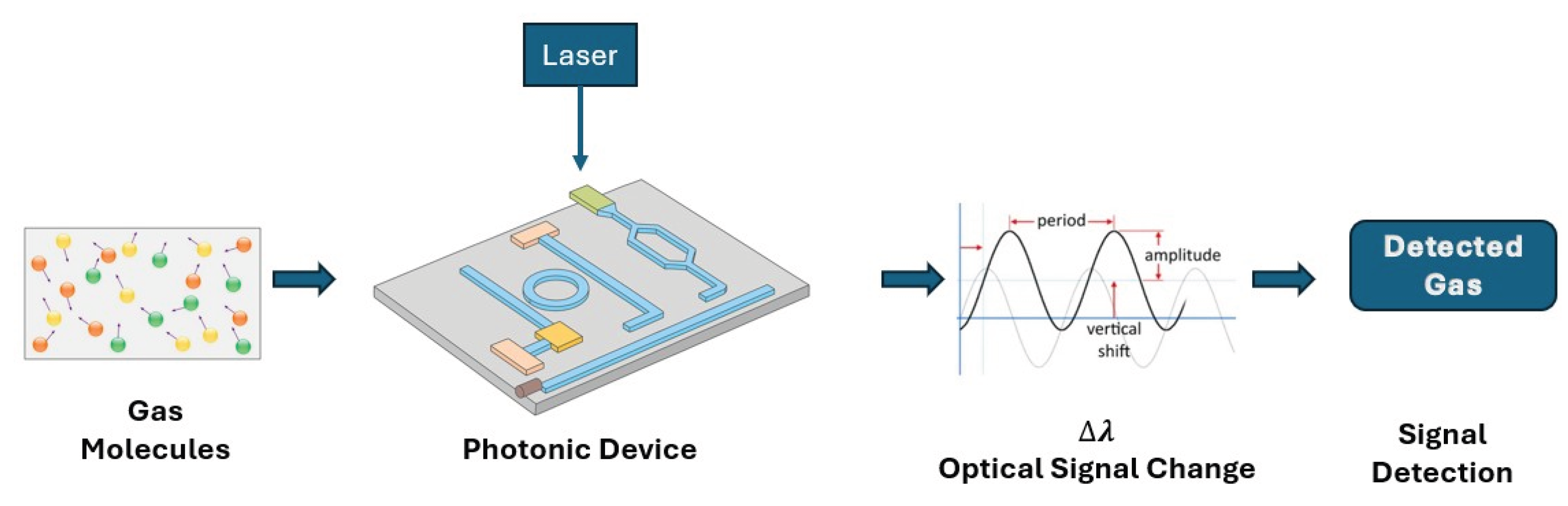
Figure 2.
A configuration of a photonic waveguide for biosensing on the SOI platform.
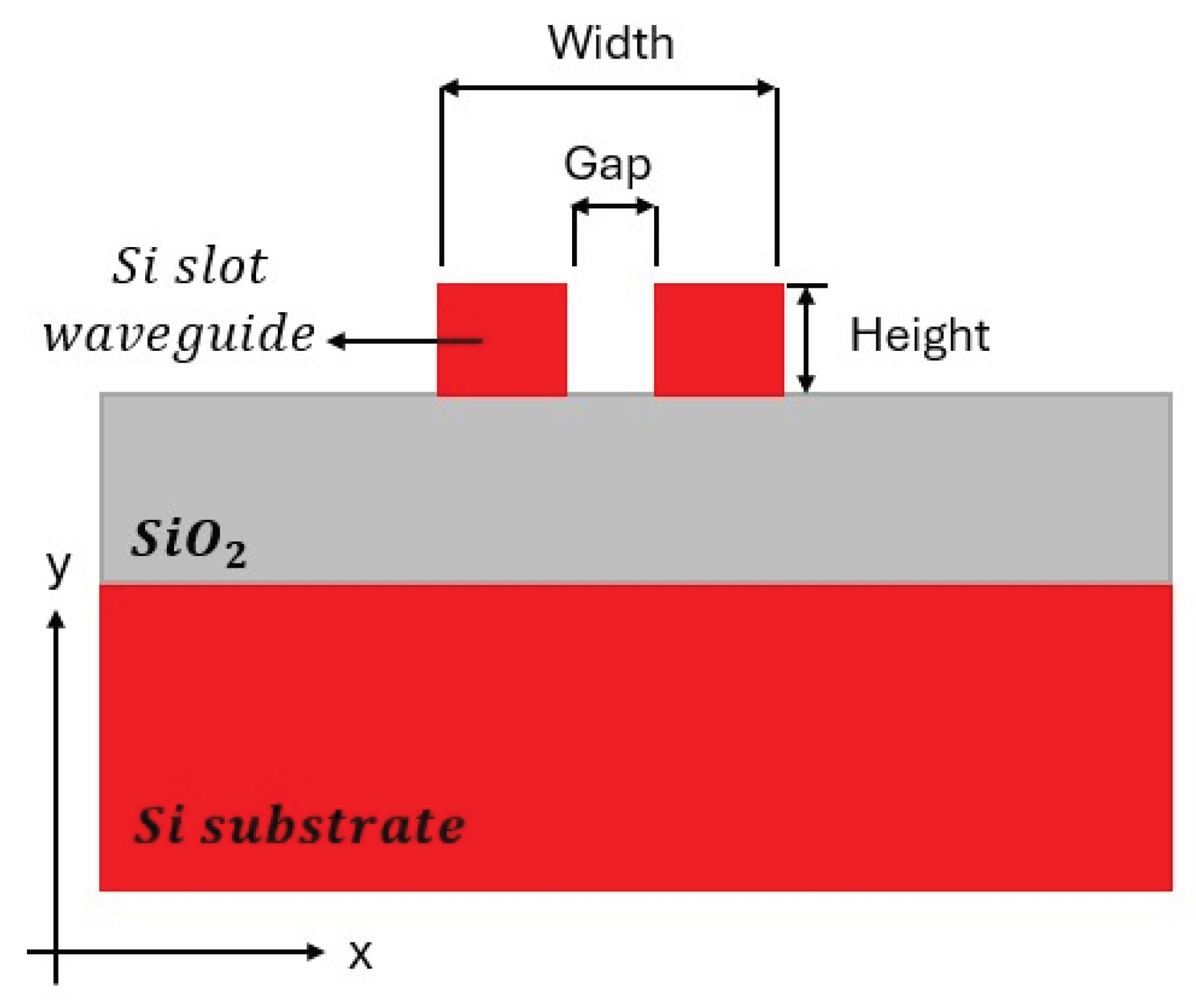
Figure 3.
A schematic of optical interconnections between the fiber and the photonic chip [47].
Figure 3.
A schematic of optical interconnections between the fiber and the photonic chip [47].
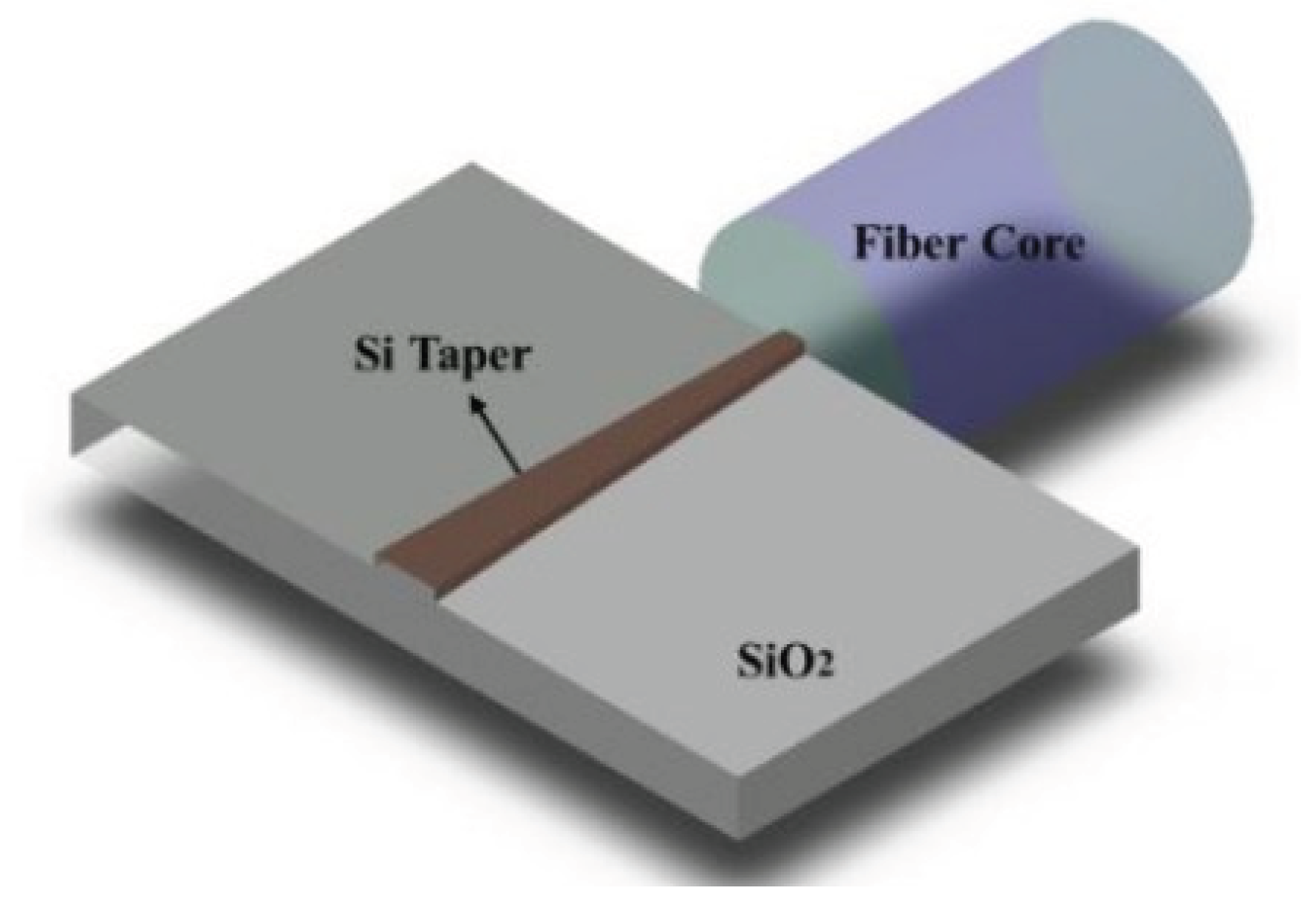
Figure 4.
The cross-sectional view of the air-clad Si3N4 waveguide structure [56].
Figure 4.
The cross-sectional view of the air-clad Si3N4 waveguide structure [56].
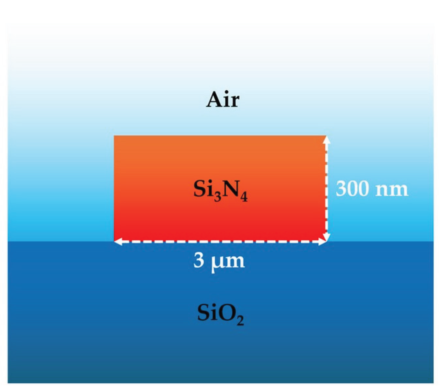
Figure 5.
Schematic showing the cleavage plane examined by X-STM/STS and the epitaxial structure of the optimized III-V-on-Si sample [61].
Figure 5.
Schematic showing the cleavage plane examined by X-STM/STS and the epitaxial structure of the optimized III-V-on-Si sample [61].
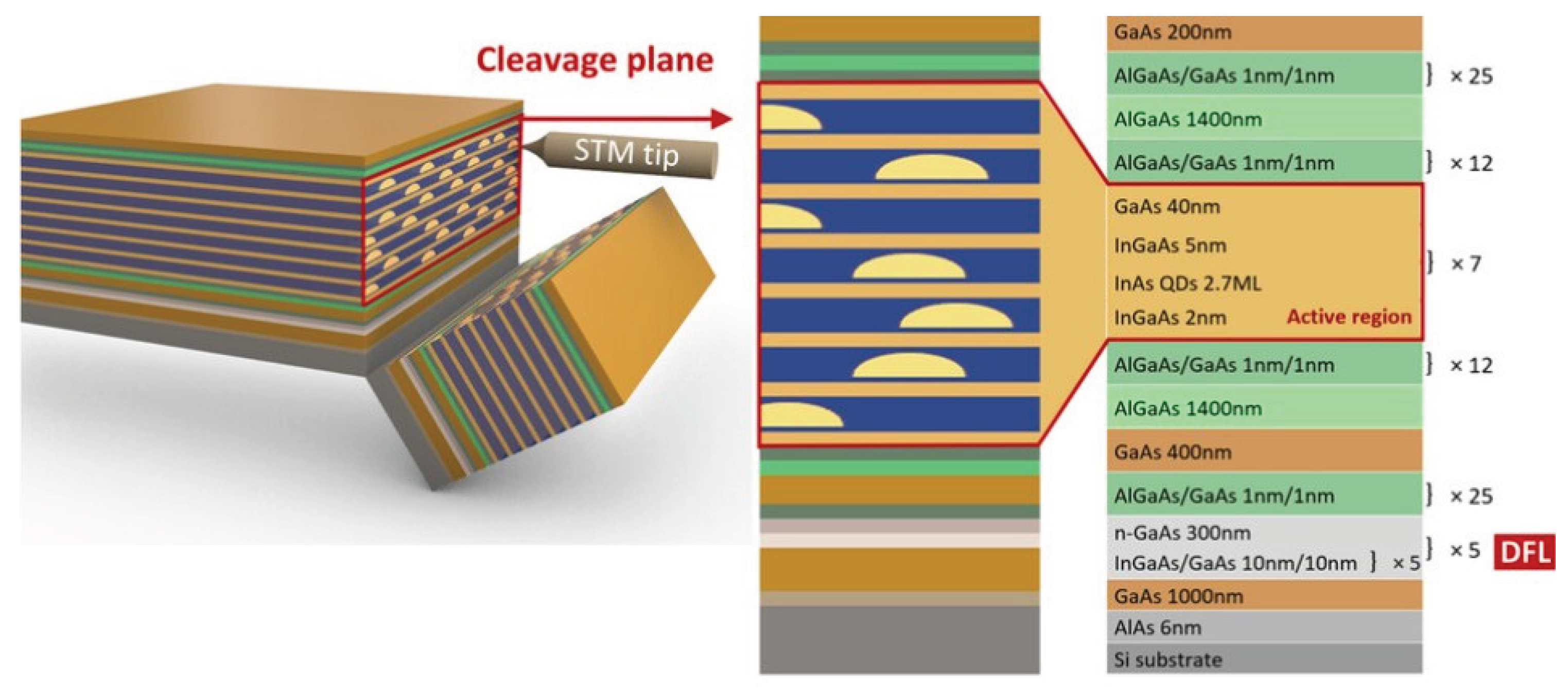
Figure 6.
An illustration of a gas sensor circuit utilizing graphene-based 2D materials [73].
Figure 6.
An illustration of a gas sensor circuit utilizing graphene-based 2D materials [73].
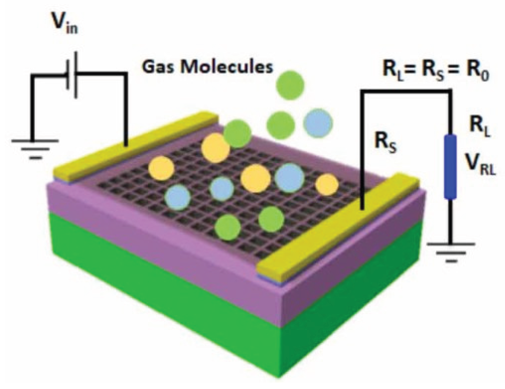
Figure 7.
An illustration of the gold nanoring array-based sensor [78].
Figure 7.
An illustration of the gold nanoring array-based sensor [78].
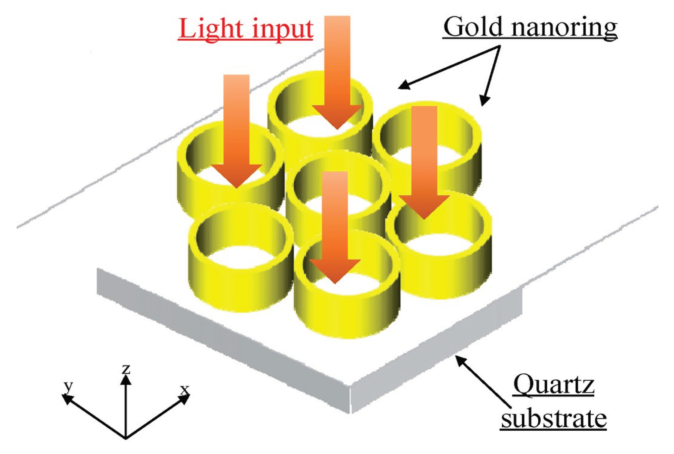
Figure 8.
An illustration of the process of lithium niobate on insulator [86].
Figure 8.
An illustration of the process of lithium niobate on insulator [86].
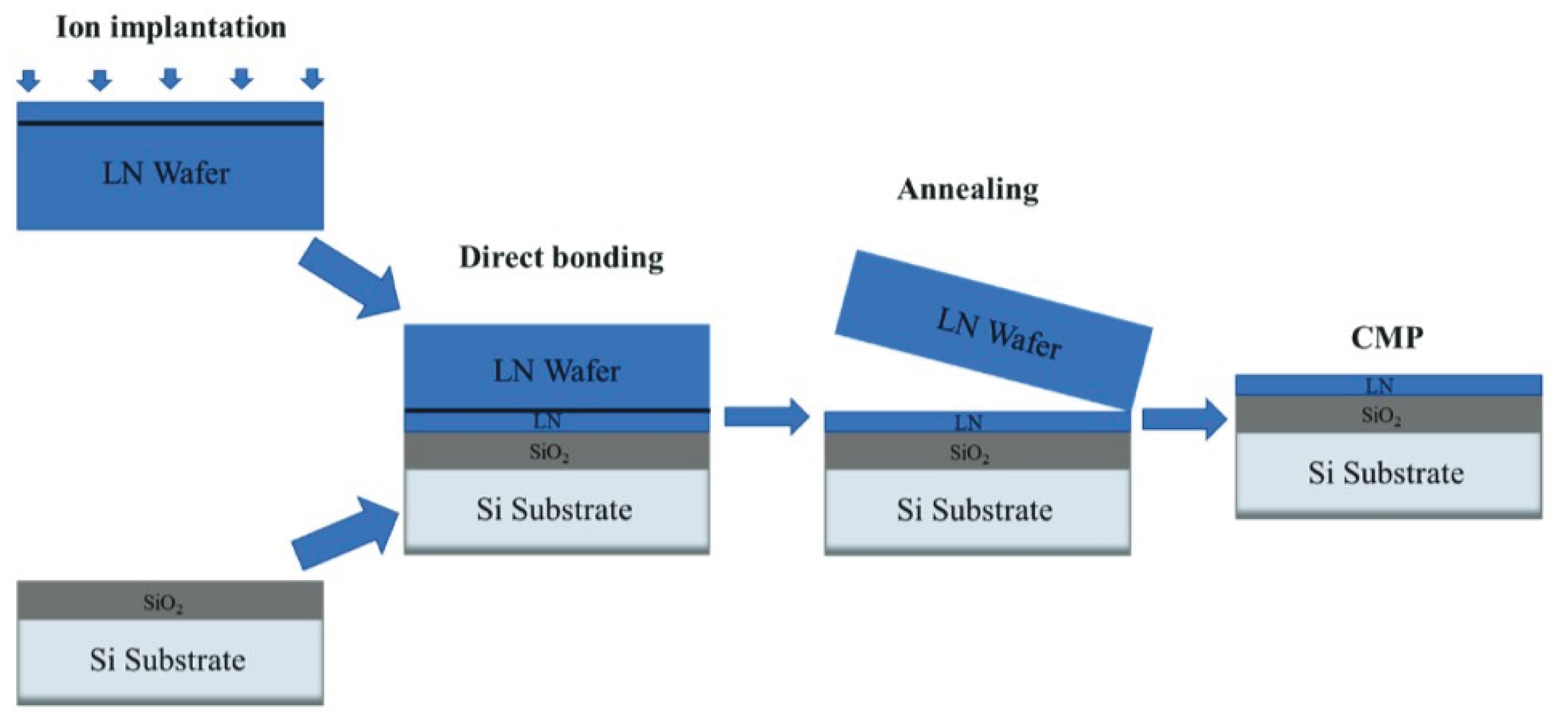
Figure 9.
Simulation and analysis of benzocyclobutene (BCB) Mach–Zehnder waveguides for portable health monitoring [90].
Figure 9.
Simulation and analysis of benzocyclobutene (BCB) Mach–Zehnder waveguides for portable health monitoring [90].
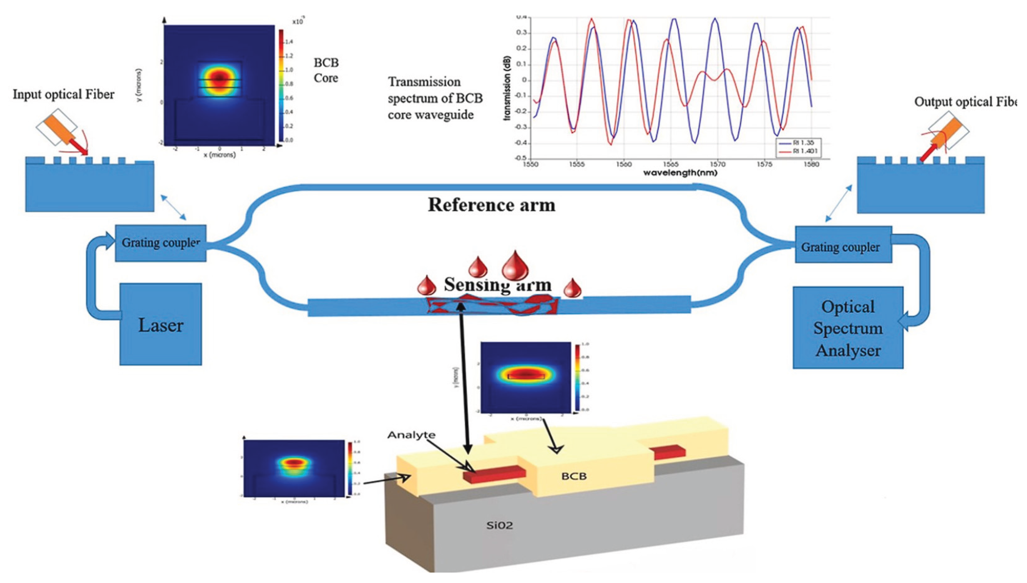
Figure 10.
A visualization of soliton microcomb generation, including dark-pulse solitons, in a ChG-based integrated micro resonator [97].
Figure 10.
A visualization of soliton microcomb generation, including dark-pulse solitons, in a ChG-based integrated micro resonator [97].
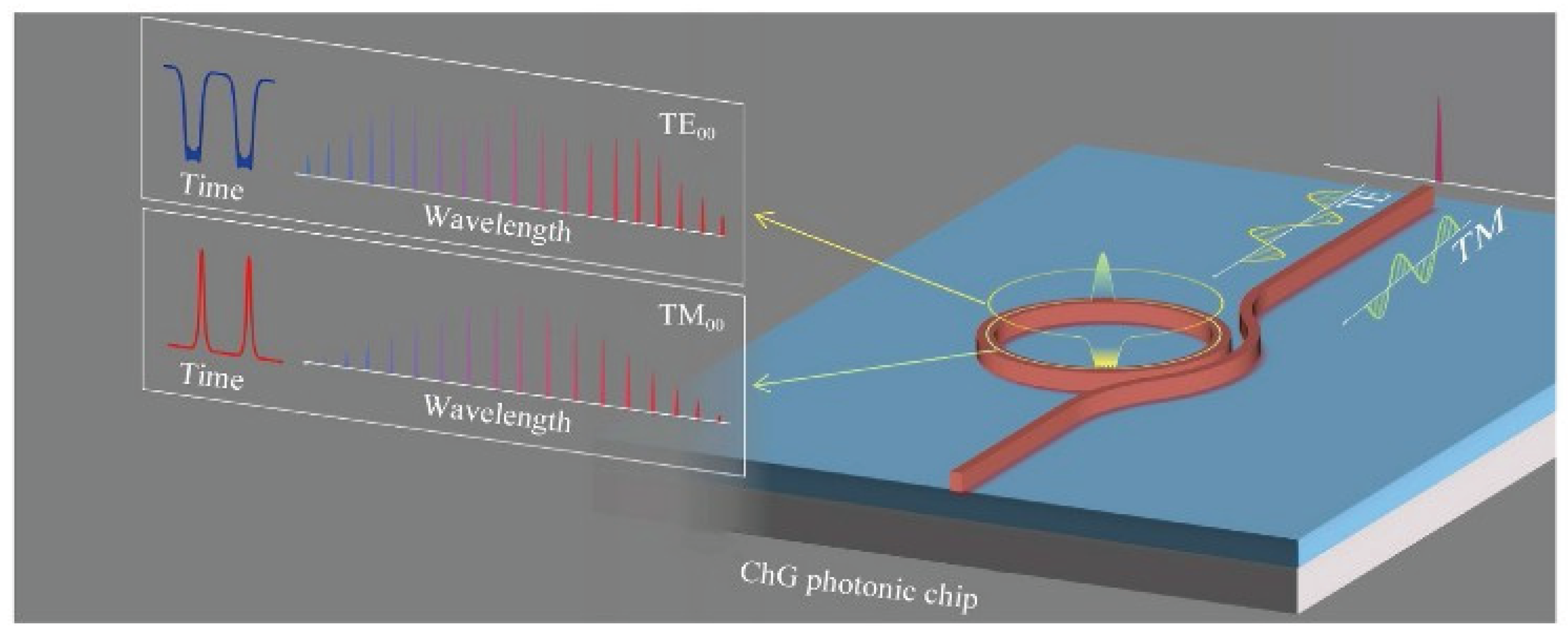
Figure 11.
The 2D electric field representation of TE (left) and TM (right) modes profiles of a silicon on insulator (SOI) rib waveguide on SiO2 substrate [102].
Figure 11.
The 2D electric field representation of TE (left) and TM (right) modes profiles of a silicon on insulator (SOI) rib waveguide on SiO2 substrate [102].
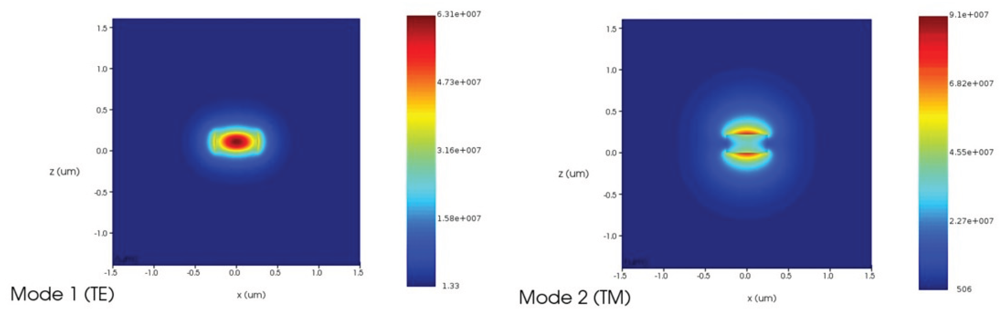
Figure 12.
The phase-shifted Bragg grating slot waveguide; (a) structural schematic and (b) transmission and reflection spectra of SP-PSBG [107].
Figure 12.
The phase-shifted Bragg grating slot waveguide; (a) structural schematic and (b) transmission and reflection spectra of SP-PSBG [107].
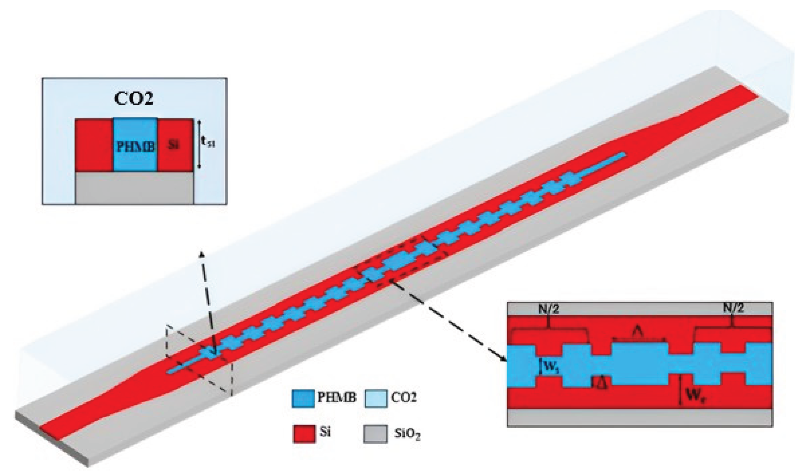
Figure 13.
An illustration of a Si3N4 ridge waveguide with the inset showing the normalized electric field distribution at 1550 nm [112].
Figure 13.
An illustration of a Si3N4 ridge waveguide with the inset showing the normalized electric field distribution at 1550 nm [112].
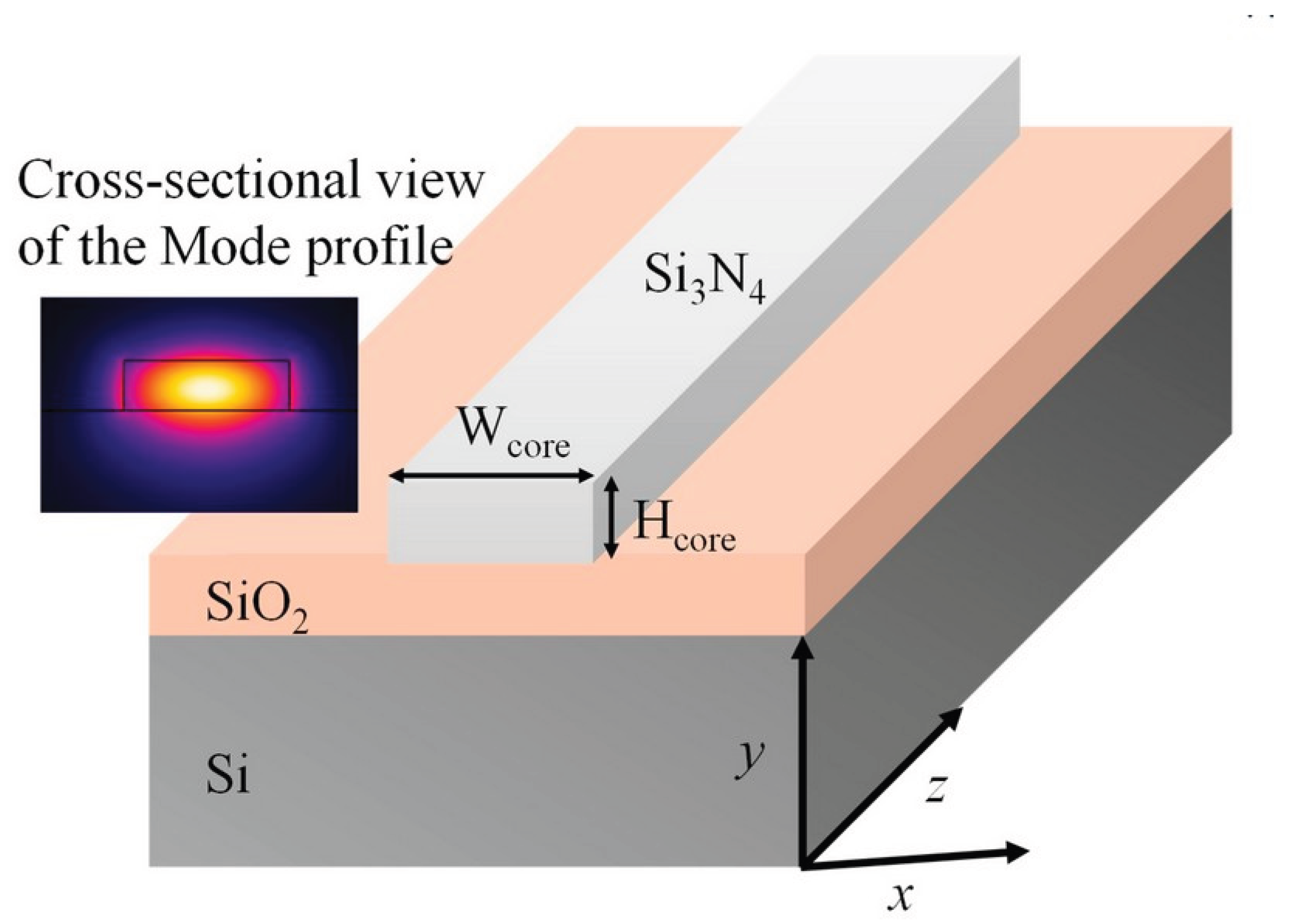
Figure 14.
A 2D illustration of the slotted ChG/SiO2 waveguide sensor.
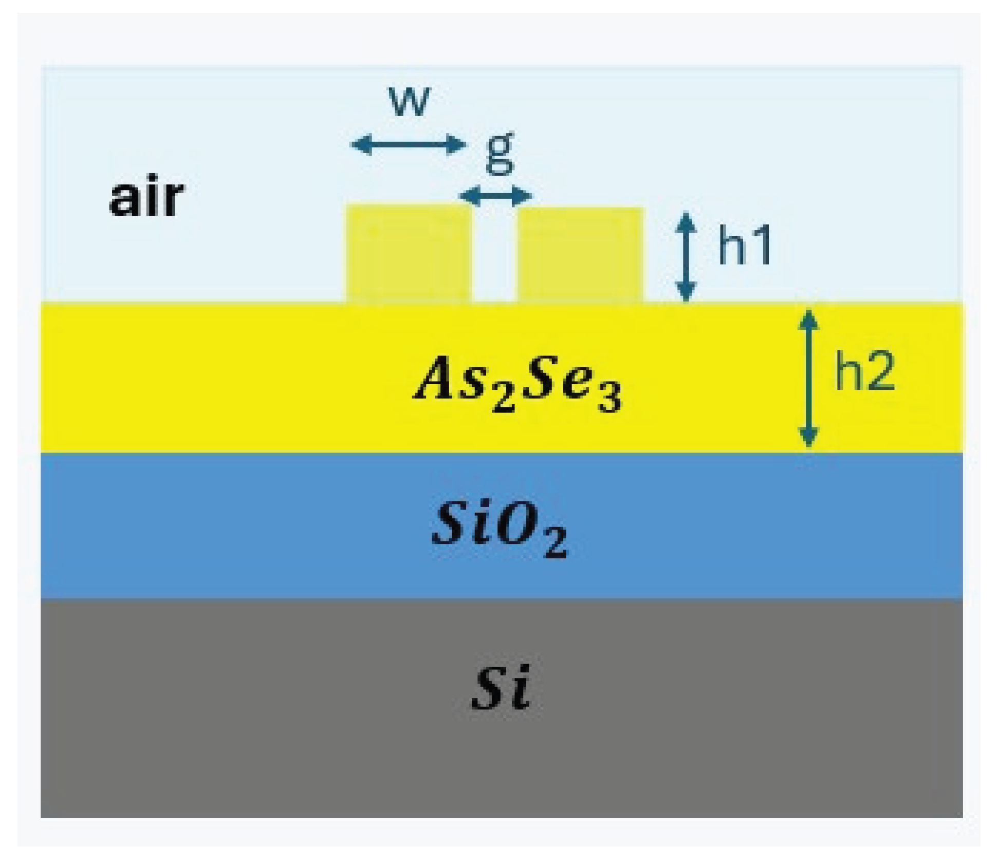
Figure 15.
The Si–LN hybrid waveguide; (a) the working mechanism and (b) the corresponding cross-sectional schematic of the waveguide structure [115].
Figure 15.
The Si–LN hybrid waveguide; (a) the working mechanism and (b) the corresponding cross-sectional schematic of the waveguide structure [115].
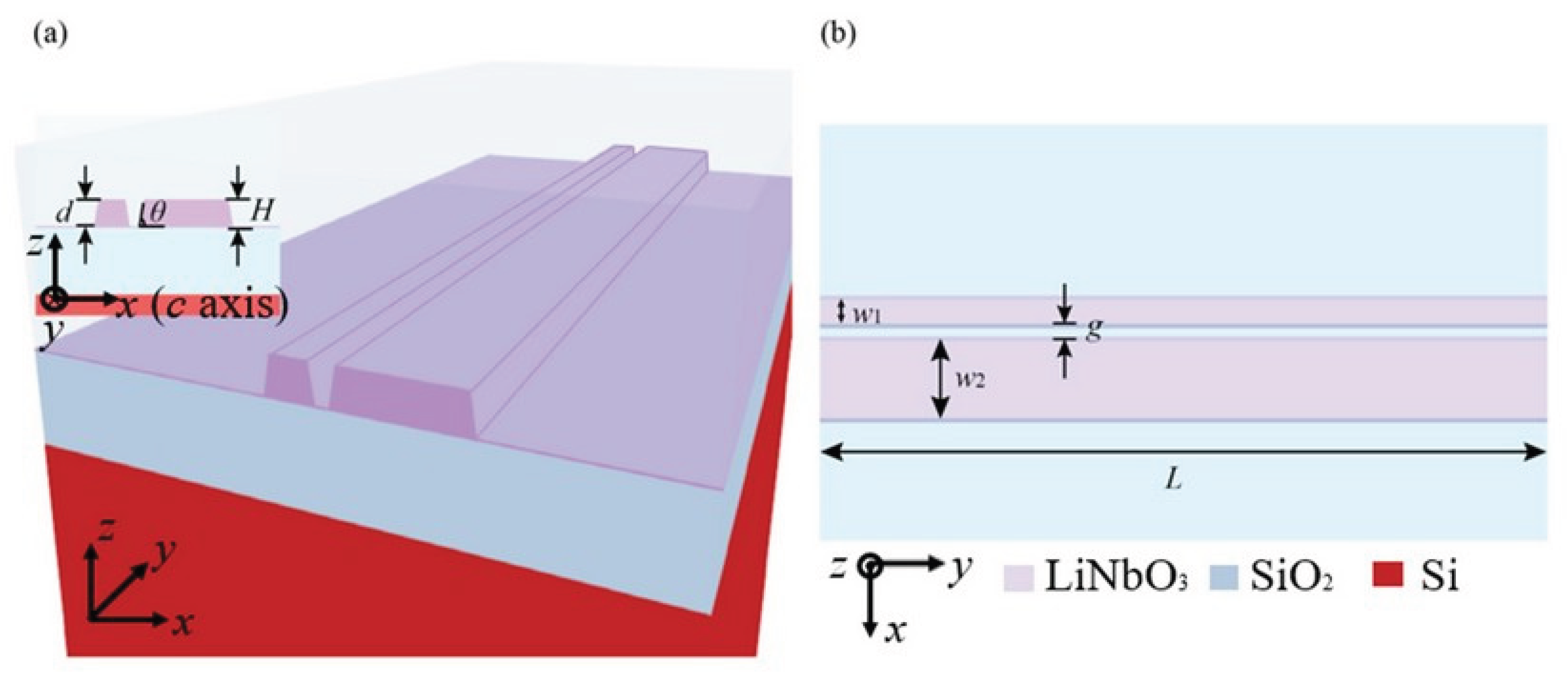
Figure 16.
A schematic of a sensor utilizing polymer waveguide platforms (a) 3D representation of the waveguide geometry and (b) the corresponding cross-section of the waveguide [116].
Figure 16.
A schematic of a sensor utilizing polymer waveguide platforms (a) 3D representation of the waveguide geometry and (b) the corresponding cross-section of the waveguide [116].
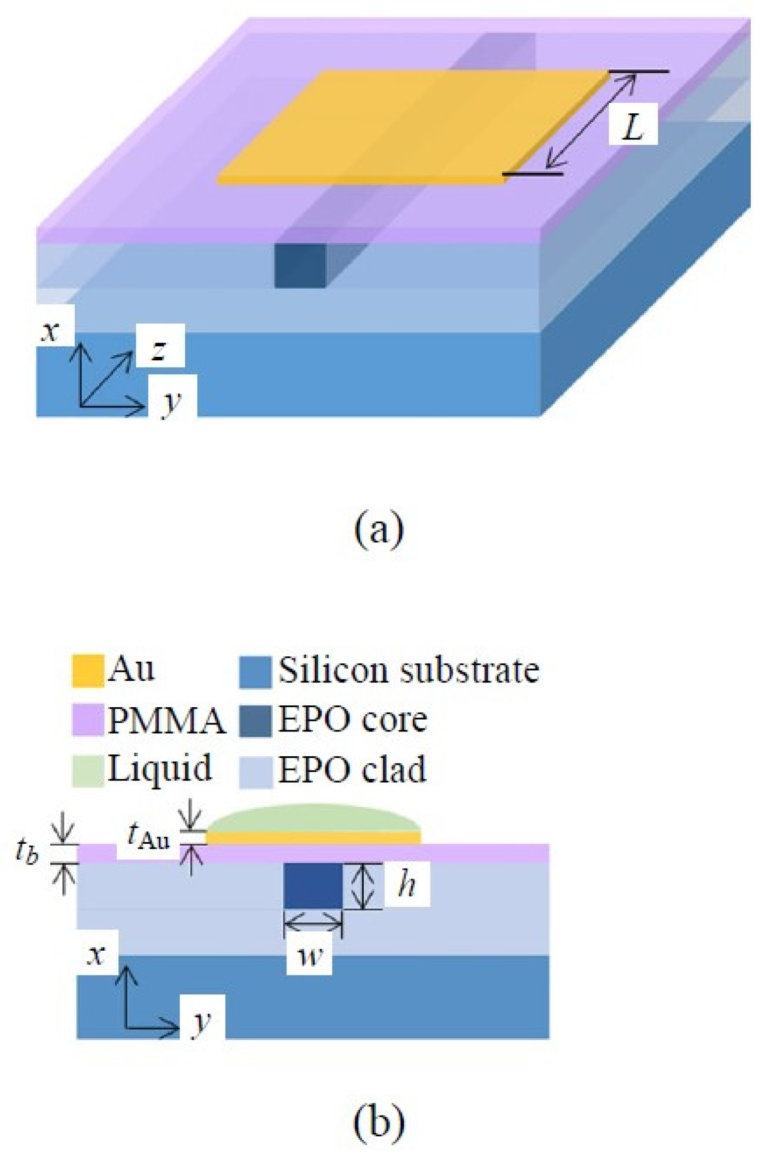
Figure 17.
Device layout and waveguide simulation: (a) cross-sectional schematic of the encapsulated graphene waveguide-integrated thermal emitter, showing the electrical connections used for Joule heating-induced thermal emission, (b) top-view schematic of the PIC components, (c) false-colored scanning electron micrograph of the device before encapsulation, and (d) simulated electric field distribution of the fundamental TE mode within the waveguide, highlighting the constituent materials [117].
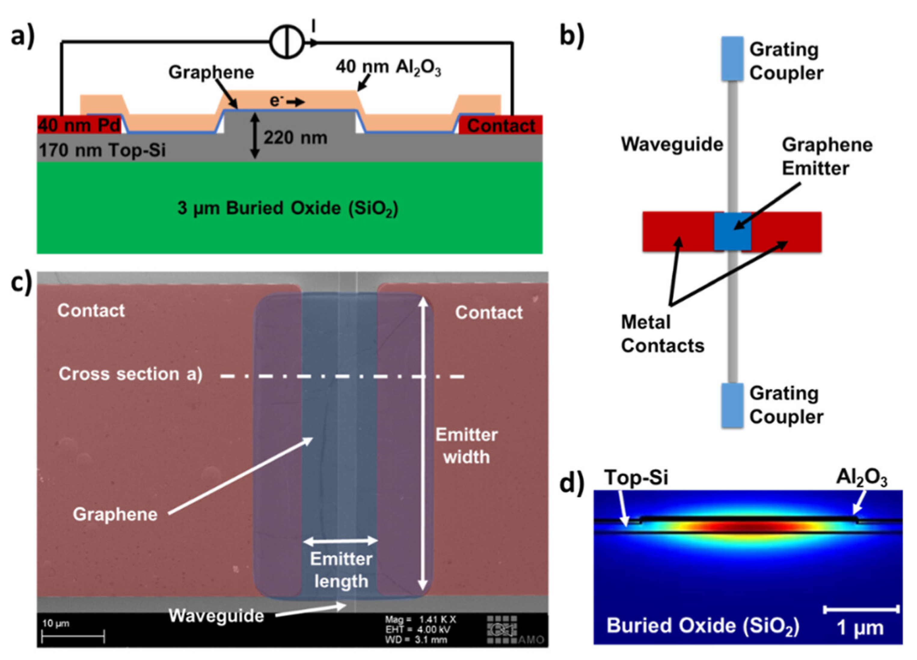
Figure 18.
A 3D perspective and cross-sectional views of the design of the MRR [124].
Figure 18.
A 3D perspective and cross-sectional views of the design of the MRR [124].
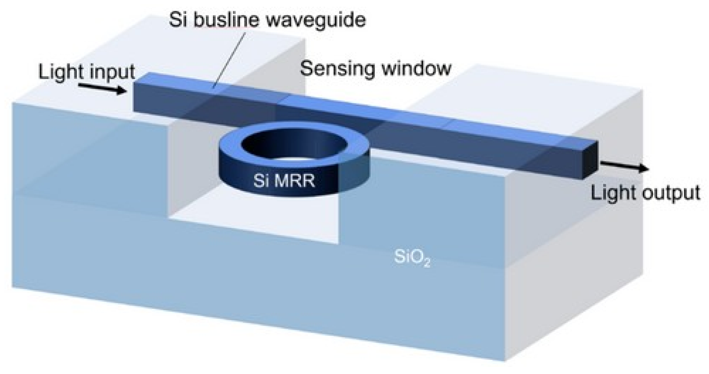
Figure 19.
An illustration of a Si3N4 racetrack resonator on silica [125].
Figure 19.
An illustration of a Si3N4 racetrack resonator on silica [125].
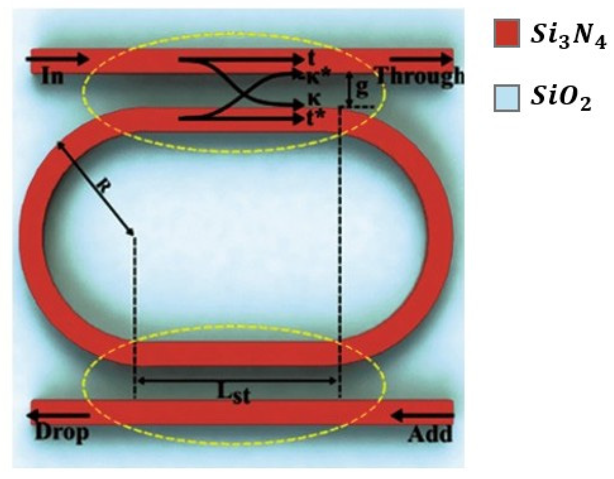
Figure 20.
Micro-ring resonator (MRR) schematic showing the geometric parameters, coupling regions, and coupling coefficients, along with the corresponding transmission spectra [125].
Figure 20.
Micro-ring resonator (MRR) schematic showing the geometric parameters, coupling regions, and coupling coefficients, along with the corresponding transmission spectra [125].
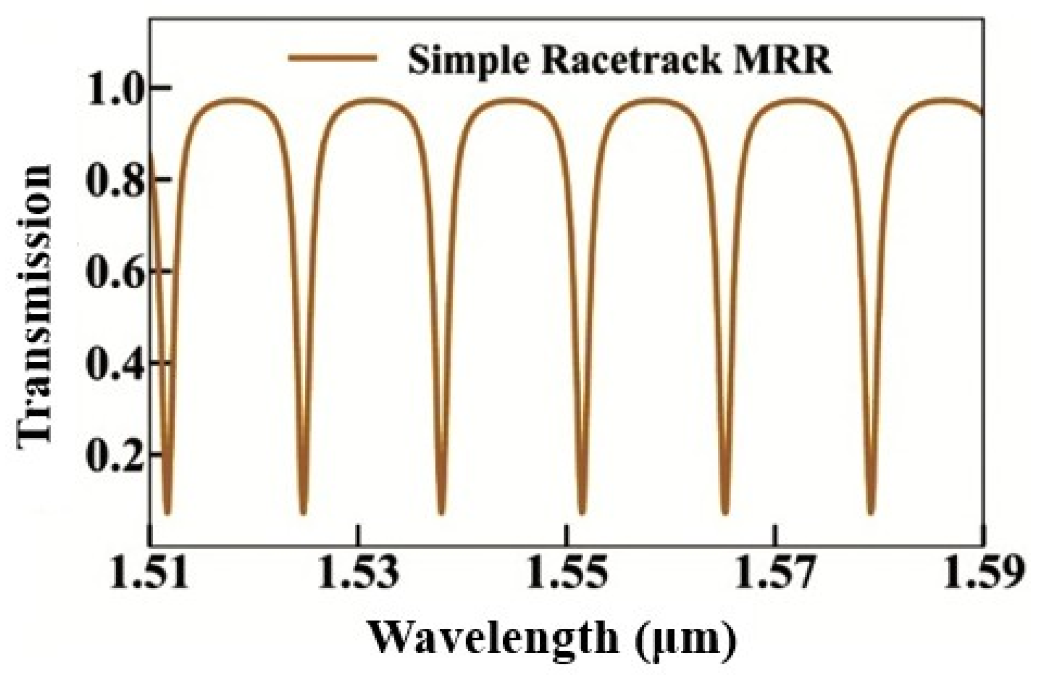
Figure 21.
An Illustration of the microring resonator structure [128].
Figure 21.
An Illustration of the microring resonator structure [128].
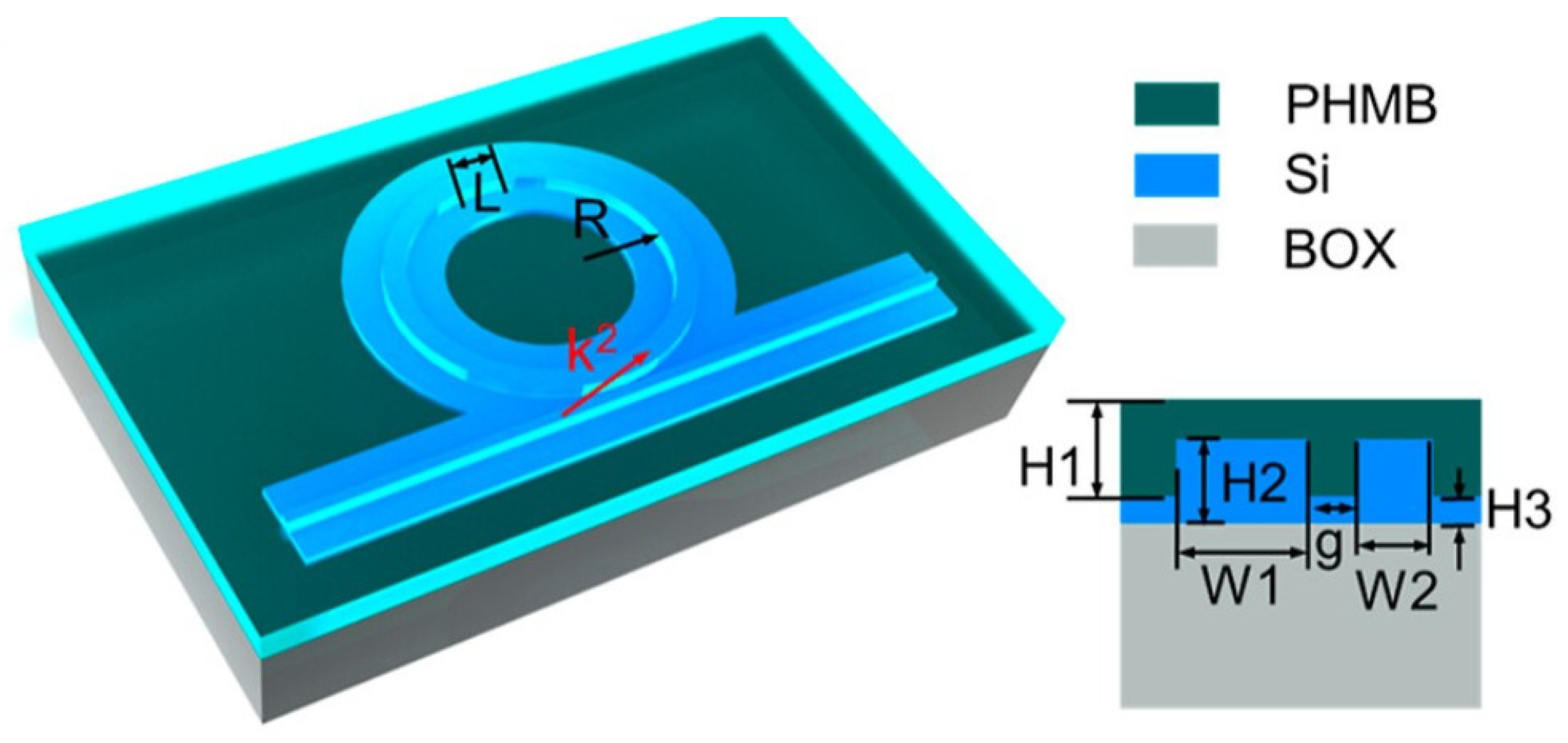
Figure 22.
The normalized transmission spectrum of the microring resonator with polyhexamethylene biguanide (PHMB) coated polymer [128].
Figure 22.
The normalized transmission spectrum of the microring resonator with polyhexamethylene biguanide (PHMB) coated polymer [128].
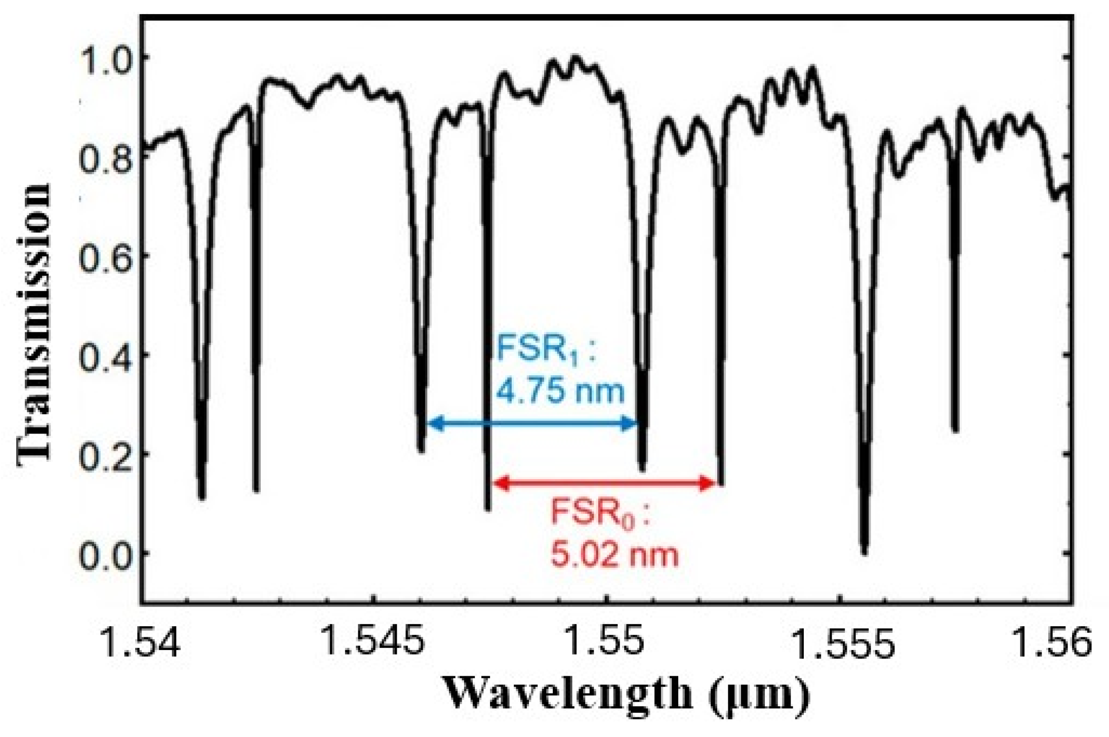
Figure 23.
A schematic of a narrowband perfect absorber (PA) designed with a silicon nanocylinder metasurface. The inset (bottom left) illustrates the periodic arrangement of silicon meta-atoms (MAs) on a gold layer, while the inset (top right) presents the corresponding transmission, reflection, and absorption spectra [13].
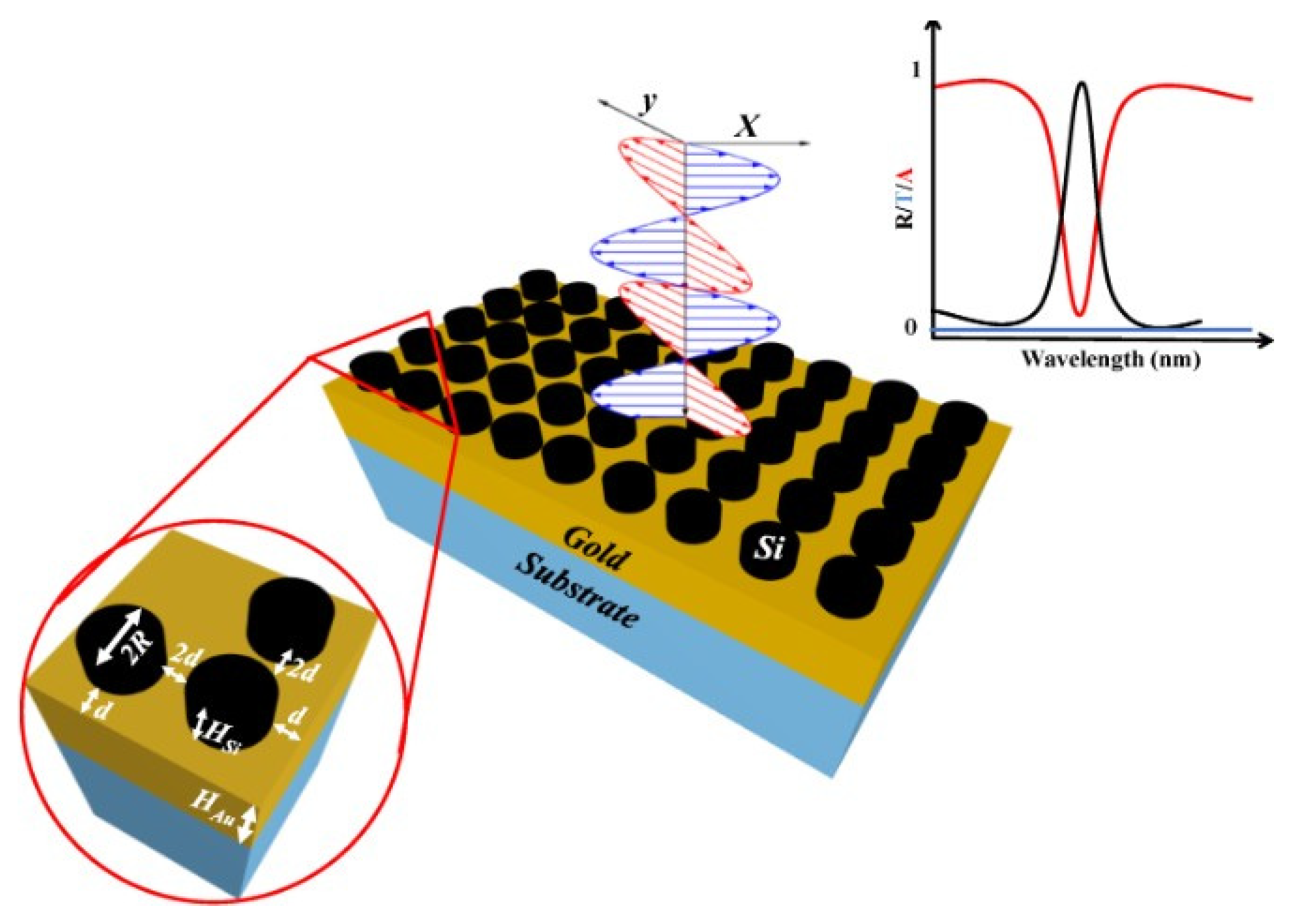
Figure 24.
A 3D schematic of the LT-MZI gas sensor with insets showing cross-sectional views of the strip waveguide (reference arm) and slot waveguide (sensing arm) [41].
Figure 24.
A 3D schematic of the LT-MZI gas sensor with insets showing cross-sectional views of the strip waveguide (reference arm) and slot waveguide (sensing arm) [41].
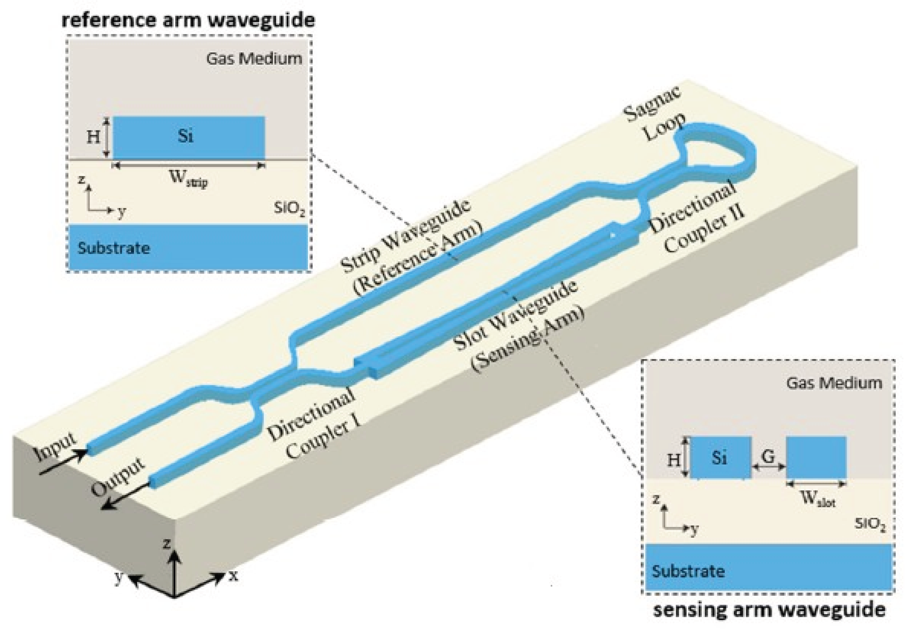
Figure 25.
The figure of merit (FOM) of the LT-MZI sensor as a function of interferometer arm length [41].
Figure 25.
The figure of merit (FOM) of the LT-MZI sensor as a function of interferometer arm length [41].
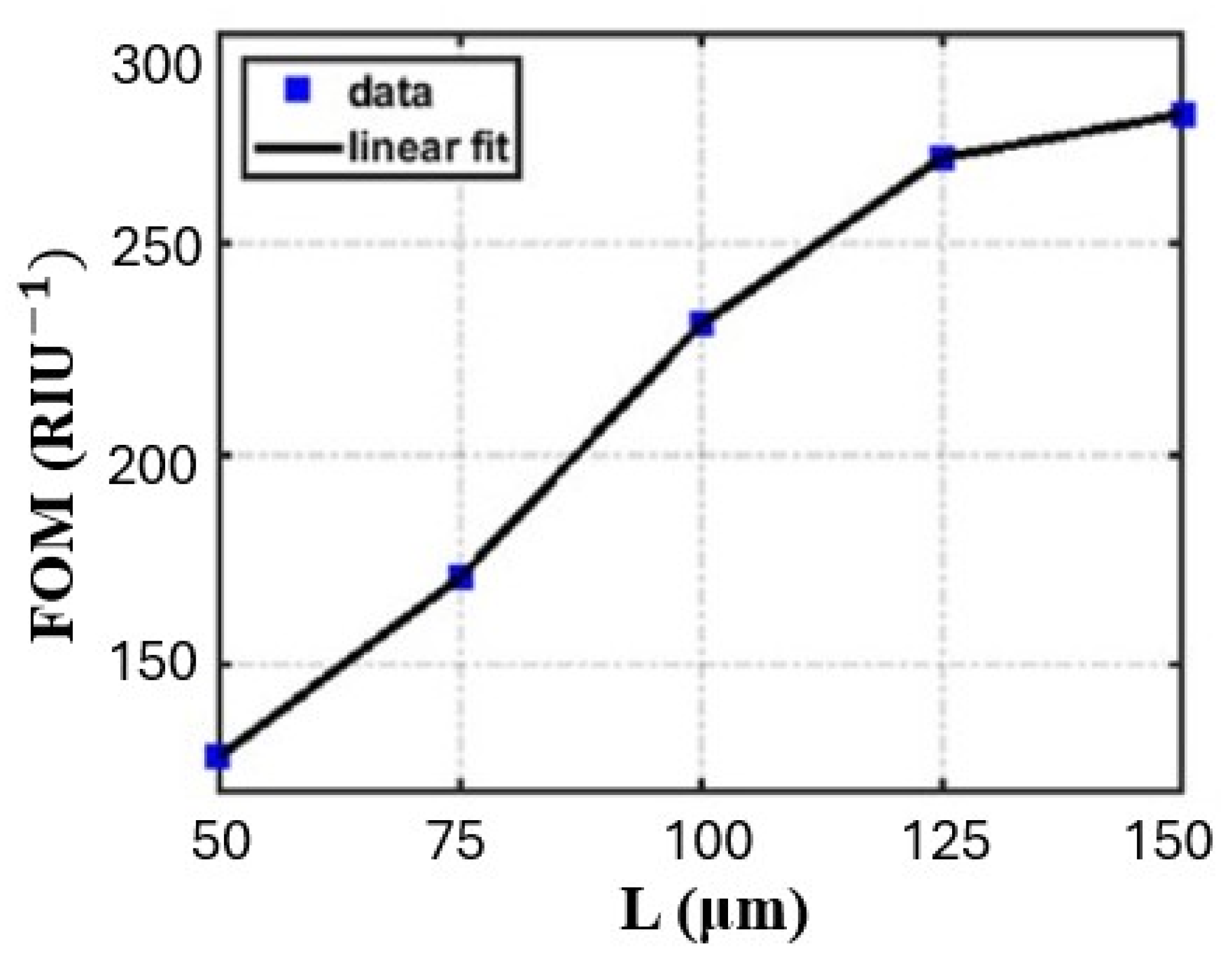
Figure 26.
A schematic of the MZI structure incorporating a multimode-fiber–thin-core-fiber–multimode-fiber (MMF–TCF–MMF) [44].
Figure 26.
A schematic of the MZI structure incorporating a multimode-fiber–thin-core-fiber–multimode-fiber (MMF–TCF–MMF) [44].
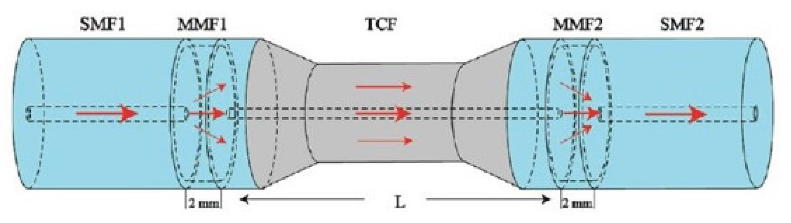
Figure 27.
The variation in the transmission spectrum of the sensor with ammonia gas concentrations from 0 to 151 ppm [44].
Figure 27.
The variation in the transmission spectrum of the sensor with ammonia gas concentrations from 0 to 151 ppm [44].
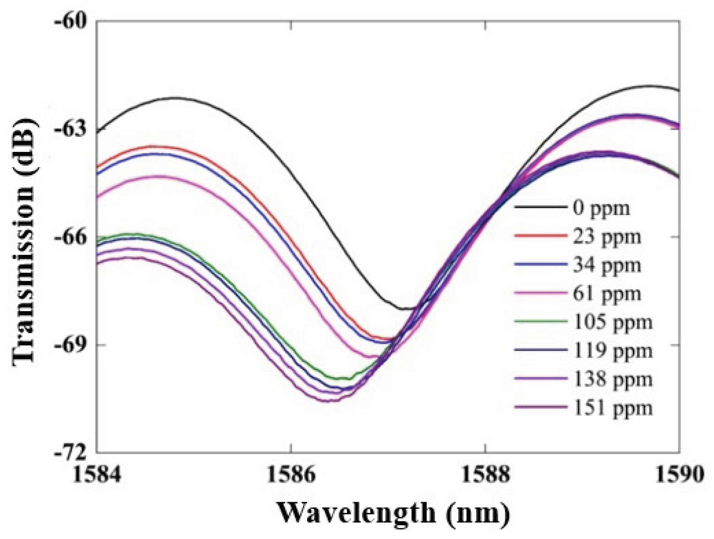

Table 1.
Comparative Analysis of Key Performance Metrics for Various Photonic Gas Sensors.
| Ref. # | Material Platform |
Device Architecture |
Sensing Gas | Sensitivity |
|---|---|---|---|---|
| [107] | SOI | Slotted Bragg grating waveguide | CO2 | 14.4 pm/ppm |
| [109] | Slot and strip waveguide | Different gases | 1,320 nm/RIU | |
| [113] | Chalcogenide Glass (GeSbSe) | Waveguide | Different gases | N/A |
| [86] | Lithium Niobate (LN) | Rib waveguide | Different gases | N/A |
| [91] | PMMA with a ZIF-8 (MOF) coating | Ridge Waveguide | CO2 | N/A |
| [117] | Graphene | Waveguide | CO2 | N/A |
| [128] | SOI | Microring | CO2 | High |
| [112] | Racetrack Ring Resonator | Different gases | 116.3 nm/RIU to 143.3 nm/RIU | |
| [126] | All-polymer (SU-8) | Whispering Gallery Mode (WGM) Microdisk Resonator | Pentanoic Acid (and other VOCs) | High |
| [89] | Plasmonic metasurface (Silicon nano-cylinders on a gold layer) | Metasurface-based perfect absorber microdisks | CO2 | High |
| [41] | SOI | Loop-terminated Mach-Zehnder Interferometer (LT-MZI) | Different gases | 1070 nm/RIU |
| [44] | Graphene Oxide (GO) | Mach-Zehnder Interferometer (MZI) with a hybrid MMF-TCF-MMF structure | NH3 | High |
Disclaimer/Publisher’s Note: The statements, opinions and data contained in all publications are solely those of the individual author(s) and contributor(s) and not of MDPI and/or the editor(s). MDPI and/or the editor(s) disclaim responsibility for any injury to people or property resulting from any ideas, methods, instructions or products referred to in the content. |
© 2026 by the authors. Licensee MDPI, Basel, Switzerland. This article is an open access article distributed under the terms and conditions of the Creative Commons Attribution (CC BY) license.
Copyright: This open access article is published under a Creative Commons CC BY 4.0 license, which permit the free download, distribution, and reuse, provided that the author and preprint are cited in any reuse.


