
Submitted:
19 January 2026
Posted:
19 January 2026
You are already at the latest version
Abstract
In 180 nm CMOS process, an enhanced dynamic bias comparator with reference-compensated offset calibration technique is implemented. In order to reduce the delay time of the comparator, an enhanced structure is used. To reduce the power consumption, a dynamic bias technique is applied to the comparator. A novel reference-compensated offset calibration technique is introduced to achieve offset calibration. Simulation results indicate that the proposed comparator achieves a delay time of 190.3 ps and an energy consumption of 324.2 fJ/comparison under operating conditions of 150 MHz and an input differential amplitude of 0.1 V. Furthermore, the application of a reference-compensated offset calibration technique facilitated a reduction in the offset voltage of the comparator from 18.1 mV to 6.3 mV.
Keywords:
comparator
; dynamic bias
; reference-compensated
; offset calibration
; analog-to-12 digital converter
1. Introduction
Analog-to-digital converters (ADCs) are essential in most systems because electronic devices handle digital data, whereas real-world signals are analog. These converters are now widely used in high-speed high-precision analog front-end circuits for integrated circuit testing, medical imaging, and instrumentation [1,2,3]. In ADCs, comparators are an essential component. Their main function is to quantize the input signal by comparing it to a reference signal, which produces a digital output level [4]. They determine the precision, speed, area, and noise characteristics of the entire ADC [5,6]. As a result, the performance of comparators is crucial to ADC.
Static and dynamic comparators are the two main types. Static comparators have very high power consumption since they are constantly operating. Their speed is also severely constrained in the absence of positive feedback [7]. Dynamic comparators overcome the issue of slow speed through clock-controlled positive feedback, which exhibit no static power consumption [8,9]. Conventional single-stage dynamic comparators require a high voltage margin because they directly stack the input transistor with a cross-coupled differential latch [10]. Single-stage dynamic comparators have advantages in static power consumption, but high-speed circuits cannot be satisfied by their sluggish speed. The two-stage dynamic comparator consists of two sections [11,12,13,14]: the first stage is a pre-amplifier, which amplifies the input signal to increase the sensitivity of the comparator while isolating kickback noise generated by the second stage. The dynamic latch in the second stage amplifies the difference between the output signals of the pre-amplifier and uses positive feedback to determine which input signal is greater. However, the low gain of the first-stage pre-amplifier restricts its capacity to efficiently amplify the input signal. This limitation also leads to inadequate noise suppression performance, which has a detrimental effect on the speed and accuracy of the comparator [15]. Therefore, developing a technique to enhance the speed of comparators is crucial.
Another important performance metric is comparator mismatch, which is typical characterized by offset voltage. Significant physical and electrical mismatches can still occur even with the most symmetrical arrangement and the minimal distances between transistors in layout [17]. Static mismatch and dynamic mismatch are two types of mismatch. The performance of the comparator is deteriorated by both kinds of mismatch since they produce an arbitrary offset voltage [18,19].
Simply increasing transistor size is not an optimal solution because this improvement is limited and also raises power consumption and parasitic capacitance. Offset calibration for a comparator can be accomplished in either the digital or analog domain. Digital calibration can be achieved through digital signal processing circuits or dedicated digital logic, whereas most analog calibration methods require the use of a digital-to-analog converter (DAC). The basic idea behind existing calibration schemes is to introduce a controlled imbalance to compensate for comparator mismatch. These methods include current compensation [9], load compensation [20,21], and threshold compensation [22]. In addition to the hardware overhead of the digital circuitry, these techniques require additional analog circuits to assist in the process of the offset calibration. This inevitably increases the design complexity, area, and power consumption of the analog system.
This paper proposes an enhanced structure to increase the speed of the comparator. A dynamic bias technique is applied to reduces power consumption. Moreover, a reference-compensated offset calibration is suggested to improve the mismatch performance of the comparator. The remainder of this paper is organized as follows. The structure of the proposed comparator is introduced in Section 2. The reference-compensated offset calibration technique is described in Section 3. The simulation results are shown in Section 4. Finally, a discussion is provided in Section 5.
2. Analysis and Design of Comparator
2.1. Analysis of Conventional Comparator
A conventional singe-stage comparator circuit is shown in Figure 1 [16]. The entire circuit consists of two parts: a dynamic comparator and a clock-gated latch. The comparator makes a decision based on the input signal and generates an output using positive feedback. The clock gated latch stores the output data and enhances the output drive capability.
When clock CK is high, the circuit is in the reset state. MP3 is off, and MN3 and MN4 are turned on, nodes X and Y are discharged to . In the clock-gated latch, and are reset to .
When clock CK goes low, the comparator begins to work. MP3 is turned on, and MN3 and MN4 are turned off. MN1 and MN2 charge the parasitic capacitances and at nodes X and Y. The voltages at node X and Y begin to increase.The time taken for voltages and to rise from to the threshold voltage is called the charge time , which can be expressed as
where equals the parasitic capacitances and of nodes X and Y. is the common-mode current. From formula (1), it can be seen that the charge time is related to the parasitic capacitance at its output node; the smaller the parasitic capacitance, the smaller the charge time. Additionally, the charge time is correlated with the common-mode current; the higher the common-mode current, the smaller the charge time. It is evident that an voltage difference between and results in amplified disparities in the charge currents of MP1 and MP2, leading to an enhancement in the voltage difference between and , which can be written as
where equals the small-signal transconductance and of input transistors MP1 and MP2, respectively. The cross-coupled pairs MN1 and MN2 become active once the voltages at nodes X and Y reach the threshold voltage . The positive feedback around these transistors eventually brings one output back to while allowing the other to rise to .
Assuming that MN1 and MN2 are in the saturation region, draw an equivalent circuit diagram as shown in Figure 2. Writing a KCL at the node X gives
Similarly, we have at the node Y
Our analysis is simplified if we only consider the differential output. The differential output can be expressed as
We thus have
where is the output resistance of the node X and Y. Assuming , formula 7 can be re-written as
Assuming the final output voltage is , the regeneration time can be calculated as
where is the differential input voltage, and equals to .
Thus the total delay of the comparator can be given as
As demonstrated in formula 11, an increase in the common-mode current is associated with a decrease in the charging time and an increase in the regeneration time . This occurs because a higher the common-mode current shortens the time needed for the parasitic capacitance to charge to a voltage close to the threshold voltage . However, an increase in common-mode current also results in a decrease in the initial output voltage , which in turn prolongs an increase in the regeneration time .
The transconductance of MOS can be expressed as
where denotes the electron mobility of MOS, represents the gate-oxide capacitance per unit area for MOS. As can be seen from formula 12, increasing the common-mode current can increase the transconductance while maintaining the same dimensions of MOS.
As shown in Figure 3, the MATLAB simulation indicates that as the common-mode current increases, the delay of the comparator decreases. It is evident that when the common-mode current is increased from 50 to 200 , the delay decreases significantly. However, with further increase in common-mode current, the reduction in delay time becomes progressively smaller. This phenomenon can be attributed to the substantial reduction in regeneration time that is caused by the increase in common-mode current. Although the charge time also decreases, this decrease is negligible. As the common-mode current continues to increase, the regeneration time gradually approaches a a fixed lower bound.
However, excessively large common-mode currents pose a significant challenge for circuit design. Assuming both MP1 and MP2 are in the saturation region, the common-mode current can be written as
where denotes the electron mobility of MP1 and MP2, represents the gate-oxide capacitance per unit area for MP1 and MP2, and are the input common-mode voltage and the source voltage of MP1 and MP2, respectively. And is the threshold voltage of MP1 and MP2. According to formula 14, two challenges are apparent in circuit design. Firstly, excessive common-mode current requires larger input transistors. Oversized input transistor not only increase the layout area but also enlarge gate-drain parasitic capacitance, which increases the output load. Secondly, comparators must operate over a range of input common-mode voltages. Since the common-mode current is proportional to the square of the input common-mode voltage, any variation in the input common-mode voltages directly changes the common-mode current, thereby altering the delay time of the comparator. Excessively high or low common-mode voltages can cause malfunctions in comparators.
As demonstrated in the preceding analysis, it can be observed that the delay of the comparator depends on the common-mode current . It is clear that simply increasing the size of the input transistor is not the optimal approach, as parasitic capacitance increases with the size of the input transistor. This increased capacitance leads to an increase in delay and power consumption of the comparator. Furthermore, the delay of the comparator is sensitive to the common-mode voltage, and alternations in the common-mode voltage can result in substantial fluctuations in the delay.
2.2. Proposed Enhanced Dynamic Bias Comparator
It has been demonstrated that increasing the common-mode current can enhance the speed of the comparator. However, a trade-off between common-mode current and the size of the input transistor must be resolved. As shown in Figure 4, a proposed enhanced dynamic bias comparator is presented. To increase the common-mode current , additional transistors MP4 and MP5 are introduced, which provides the required common-mode current while maintains a compact size. If the common-mode current contributed by the input transistor is negligible compared to that supplied by MP4 and MP5, then the dependence of the delay on the input common-mode voltage can also be minimized. To conserve power, a dynamic bias technique is employed [23], which turns off the bias of the comparator after the comparator has completed its comparison. The effect of dynamic bias on the delay time of the comparator is negligible with the only overhead being the additional logic circuitry required. The circuit is composed of two sections: the comparator and the logic circuit. In the logic circuit section, the comparator output signals and pass through an XOR gate and a inverter, and then combined with the clock CK via a NAND gate to generate the final control signal fnh. The main purpose of the control signal fnh is to dynamically enable or disable the comparator, thereby reducing power consumption.
When the clock CK is low, the comparator is in the reset state. The control signal fnh is high, causing MP3, MP4 and MP5 to turn off, MN3 to turn on, and the comparator is disable. At the same time, MN3 connects nodes X and Y to equalize the voltages and . And the output and are reset to zero in the latch.
When the clock CK transitions from low to high, the comparator begins operation. The control signal fnh transitions from high to low, causing MP3, MP4 and MP5 to turn on while MN3 turns off. The additional current provided by MP4 and MP5 charges nodes X and Y. Simultaneously, the common-mode current from MP1 and MP2 also charges nodes X and Y. During this process, the input signals and provide differential current to nodes X and Y through MP1 and MP2. This stage is referred to as the charging phase of the comparator.
The cross-coupled pairs MN1 and MN2 becomes active once the voltages at nodes X and Y reach the threshold voltage . The positive feedback around these transistors eventually brings one output back to zero while allowing the other to rise to . Subsequently, the latch stores the outputs of the comparator and pass them to the subsequent stage.
Once the output is settled, the output voltages and are always at complementary levels ( and , respectively). Consequently, the control signal fnh transitions from a low level to a high level, disabling the bias of the comparator and reducing its dynamic power consumption. When the clock CK goes low, the comparator and the latch re-enter the reset state. Voltages and are reset to zero, while voltages and are reset to near the threshold voltage . As the clock CK is low, the control signal fnh remains high, waiting for the next enable cycle.
The proposed enhanced dynamic bias comparator offers two main advantages. First, the addition of auxiliary current paths accelerates the speed of the comparator. Second, dynamic bias of the comparator is achieved through the implementation of simple logic circuits. This reduces the power consumption of the comparator, thereby enhancing its overall energy efficiency.
3. Design of the Offset Calibration Technique
3.1. Working Principle of the Comparator
As shown in Figure 5, the circuit diagram and timing diagram of a comparator with offset for voltage comparison is presented. During the sampling phase, the clock is high, while the clock is low. The top plates of sampling capacitors and are connected to the common-mode voltage , while their bottom plates are connected to the input signals and , respectively. At time , the voltage across the sampling capacitor can be written as
During the comparison phase, the clock goes low, while the clock goes high. The bottom of sampling capacitors and are connected to the reference signals and , respectively. At time , the comparator begins operation. At this moment, the voltages at nodes X and Y can be expressed as
Subtracting formula 17 from formula 18, the input differential voltage of the comparator can be expressed as
The supplementary equation is as follow
From formula 22, it is evident that the presence of the offset voltage results in a shift of the reference comparison point of the comparator by an amount equivalent to . If the offset voltage of the comparator is large, it will have a detrimental effect on the performance of the analog-to-digital converter.
3.2. Proposed Reference-Compensated Offset Calibration Technique
As shown in Figure 6, the schematic diagram of the comparator with reference-compensated technique is presented. The alteration of reference voltage at the comparison point serves as a method to compensate for the offset voltage of the comparator. When the reference voltage is changed, formula 22 can be rewritten as
From formula 23, it can be seen that when equals , the offset voltage of the comparator can be eliminated. The step size of is directly proportional to the precision of the calibration. Higher calibration accuracy corresponds to a smaller step size of , whereas lower accuracy requires a larger step size of .
As illustrated in Figure 7, the schematic diagram of the proposed calibration scheme is presented. The entire calibration circuit consists of four sections: the comparator under calibration, the voltage generation circuit, the counter and the digital logic control circuit. At the start of calibration, the sampling capacitor is connected to the reference voltage and via the clock during sampling phase, rather than to the input signals and . The sampling capacitor is connected to the reference voltage with a compensation offset via the clock during comparison phase. The calibration voltage represents the step size of and is directly proportional to the calibration accuracy. is a multiple of 1/2, and in this design, it takes nine values: -2, -3/2, -1, -1/2, 0, 1/2, 1, 3/2, and 2. The digital control logic commands the voltage-generation circuit to adjust the compensation level of the reference voltage. Simultaneously, the counter collects the output of the comparator ot estimate the offset magnitude.Ultimately, the compensation of the reference voltage is adjusted to an appropriate level, reducing the offset voltage to a system-acceptable value.
The control logic circuit is driven by the digital clock dclk. When the falling edge of the reset signal rst arrives, the offset calibration process of the comparator starts. If the calibration-enable signal cal is 1, the calibration circuit proceeds to the next stage; if it is 0, calibration ends. The control word co generated by the control logic is sent simultaneously to the voltage generation circuit and the counter. The default value of co is 1. The voltage generation circuit adjusts the coefficient from -2 to 2 based on the control word co ranging from 1 to 9. The counter increment is based on the current output result. The counter increments only when the comparator output dop is 1. After completing avg comparisons and counts, the algorithm determines the compensation point that exhibits the minimum offset voltage. This compensation point is then designated as the reference comparison point for the normal operation of the comparator.
In conventional pipelined ADC, the reference comparison point of the comparator is obtained from a resistive voltage divider. The voltage generation circuit can be realized by segmenting the original resistor string into smaller equal-valued resistors, thereby introducing additional reference-compensation points around the nominal comparison point. The main advantage of this approach is that it avoids extra analog circuitry, which reduces both the hardware overhead and the power consumption typically incurred by analog calibration circuits.
The reference-compensated offset calibration technique proposed in this paper achieves offset calibration for comparators without altering their structure. The analog circuit requires only a small number of additional voltage-division resistors, making this technique well-suitable for offset calibration of comparators in most pipelined ADCs.
4. Results
Figure 8 shows the typical waveforms of the proposed comparator. The simulation conditions are as follows: a supply voltage of 1.8 V, a common-mode voltage of 0.9 V, an input differential voltage of 100 mV, an operating frequency of 150 MHz, and a comparator load of 5 fF. When the rising edge of the clock CK arrives, the output voltage and develop a voltage difference of about 0.9 V within 190.3 ps. Approximately 300 ps later, the control signal fnh goes high, disabling the bias of the comparator to reduce its power consumption.
As shown in Figure 9a, the delay time of the comparator versus the differential input voltage is depicted at a fixed common-mode voltage of 0.9 V. At the differential input voltage of 0.1 mV, the proposed comparator has a delay of about 298 ps, while the conventional comparator has a delay of approximately 387 ps, which is roughly 89 ps longer. This indicates a significant advantage of the proposed comparator when processing very small input signals. Furthermore, the proposed comparator exhibits a delay time variation of approximately 115 ps over the entire differential input voltage range, compared to 172 ps for the conventional comparator, indicating that the conventional comparator has a 57 ps greater variation in delay time. These results demonstrate that the proposed comparator maintains excellent stability even under wide variations in the differential input voltage.
As shown in Figure 9b, the energy consumption of the comparator is plotted against the differential input voltage at a common-mode voltage of 0.9 V. At a differential input voltage of 0.1 mV, the energy consumption of the proposed comparator is 419 fJ/comparison, compared to 778 fJ/comparison for the conventional comparator. At 200 mV input, the corresponding values are 320 fJ/comparison and 536 fJ/comparison, respectively. These results indicated that the proposed comparator has a lower delay while consuming the same amount of energy. This is facilitated by the application of dynamic bias, which minimises the dynamic power consumption of the proposed comparator.
As shown in Figure 10a, the delay time of the comparator varies with changes in the common-mode voltage is plotted for the differential input voltage of 0.1 V. At a common-mode voltage is 0.7 V, the proposed comparator has a delay time of 185 ps. The delay increases gradually with the common-mode voltage, reaching 200 ps at 1.1 V. Over the entire common-mode voltage range, the delay variation of the proposed comparator is only about 15 ps. In contrast, the conventional comparator show a delay of 186 ps at 0.7 V. Its delay increases rapidly as the common-mode voltage rises, reaching a maximum of 390 ps at 1.1 V. The overall delay variation of the conventional comparator across the same range is about 204 ps, approximately 13 times larger than that of the proposed one. These results indicate that the proposed comparator maintains excellent performance under common-mode voltage variations, whereas the traditional comparator is significantly affected by changes in the common-mode voltage.
As shown in Figure 10b, the energy consumption of the comparator is plotted against the common-mode voltage at a differential input voltage of 0.1 V. At a common-mode voltage of 0.7 V, the energy consumption of the proposed comparator is 352 fJ/comparison, compared to 1116 fJ/comparison for the conventional one – a larger difference of 764 fJ/comparison. As the common-mode voltage increases, the energy consumption of both comparators decreases. At a common-mode voltage of 1.1 V, the energy consumption of the proposed comparator is 299 fJ/comparison, while the conventional comparator consumes 296 fJ/comparison, resulting in a much smaller difference of only 3 fJ/comparison. More importantly, over the entire common-mode voltage range, the proposed comparator exhibits a much smaller variation of 53 fJ/comparison in energy consumption, compared to 820 fJ/comparison for the conventional comparator. These results demonstrate that the proposed comparator maintains highly stable energy efficiency across common-mode voltage variations.
A Monte Carlo simulation is performed on the comparator with the common-mode voltage set to 0.9 V. The calibration step size is 15.6 mV, and the coefficients takes the values: -2, -3/2, -1, -1/2, 0, 1/2, 1, 3/2, and 2. Figure 11 presents the results of 3600-sample Monte Carlo simulation under PVT (process, voltage, temperature) variations. The offset voltage of the comparator is reduced from 18.1 mV before calibration to 6.3 mV after calibration – an improvement of 11.8 mV. As shown in Figure 12, the Monte Carlo simulation of 400-sample under TT process reveals that, before calibration, the offset voltage shows significant dispersion, with a maximum value of around 60 mV. However, after calibration, the offset voltage is constrained between approximately ± 15.6 mV, which demonstrates that the calibration technique enhances the mismatch performance of the comparator.
Table 1 compares the performance of the proposed comparator with other comparators. Fabricated the same process technology, the proposed comparator achieves a significant speed advantage, with a delay time of 190.3 ps, compared to a minimum delay time of 268 ps in other works. Compared to other comparators, the proposed comparator shows advantages in terms of power consumption. However, there is still significant room for improvement in the power consumption. Thanks to the application of offset calibration technique, the proposed comparator achieves a offset voltage of just 6.3 mV. This indicates that there is further potential for optimization in its algorithm and structure.
5. Conclusions
This paper proposes an enhanced dynamic bias comparator and employs a novel reference-compensated offset calibration technique. First, the delay of the comparator is analyzed and validated through MATLAB simulation, revealing its depends on the common-mode current. Based on this insight, a enhanced structure is introduced, which not only increases the speed of the comparator but also mitigates the impact of common-mode voltage variations on the delay. Then, a dynamic bias is applied to reduce the dynamic power consumption of the comparator. Furthermore, to address comparator mismatch, a reference compensation technique is proposed to improve mismatch performance without altering the structure of the comparator.
Author Contributions
Data curation, M.W.; Formal analysis,M.W. and L.Z.; Methodology, M.W.; Supervision, R.Y.; Validation, M.W. and Y.G.; Software, M.W. and Y.Z.; Project administration, Z.T; Writing-original draft, M.W.; Writing-review and editing, M.W. and L.Z. All authors have read and agreed to the published version of the manuscript.
Data Availability Statement
The data used in this study can be requested from the corresponding author.
Acknowledgments
The authors thank the Inbisen Semiconductor Co., Ltd for the financial and technical support. Honour the memory of Senior Brother Liang Zou!
Conflicts of Interest
The authors declare no conflicts of interest.
References
- Gonen, B.; Sebastiano, F.; Quan, R.; et al. A Dynamic Zoom ADC With 109-dB DR for Audio Applications. IEEE Journal of Solid-State Circuits 2017, 52, 1542–1550. [Google Scholar] [CrossRef]
- Hurrell, C. P.; Lyden, C.; Laing, D.; et al. An 18 b 12.5 MS/s ADC With 93 dB SNR. IEEE Journal of Solid-State Circuits 2010, 45, 2647–2654. [Google Scholar] [CrossRef]
- Maddox, M.; Chen, B.; Coln, M.; et al. A 16 bit linear passive-charge-sharing SAR ADC in 55nm CMOS. In Proceedings of the 2016 IEEE Asian Solid-State Circuits Conference (A-SSCC), Toyama, Japan, 2016; pp. 153–156. [Google Scholar]
- Bindra, H. S.; Lokin, C. E.; Schinkel, D.; et al. A 1.2-V Dynamic Bias Latch-Type Comparator in 65-nm CMOS With 0.4-mV Input Noise. IEEE Journal of Solid-State Circuits 2018, 53, 1902–1912. [Google Scholar] [CrossRef]
- Tang, X.; Liu, J.; Shen, Y.; et al. Low-Power SAR ADC Design: Overview and Survey of State-of-the-Art Techniques. IEEE Transactions on Circuits and Systems I: Regular Papers 2018, 69, 2249–2262. [Google Scholar] [CrossRef]
- Wang, T. -Y.; Li, H. -Y.; Ma, Z. -Y.; et al. A Bypass-Switching SAR ADC With a Dynamic Proximity Comparator for Biomedical Applications. IEEE Journal of Solid-State Circuits 2018, 53, 1743–1754. [Google Scholar] [CrossRef]
- Razavi, B. Charge steering: A low-power design paradigm. In Proceedings of the IEEE 2013 Custom Integrated Circuits Conference, San Jose, CA, USA, 2013; pp. 1–8. [Google Scholar]
- Nikolic, B.; Oklobdzija, V. G.; Stojanovic, V.; et al. Improved sense-amplifier-based flip-flop: design and measurements. IEEE Journal of Solid-State Circuits 2000, 35, 876–884. [Google Scholar] [CrossRef]
- Wong, K.. -L. J.; Yang, C.. -K. K. Offset compensation in comparators with minimum input-referred supply noise. IEEE Journal of Solid-State Circuits 2004, 39, 837–840. [Google Scholar] [CrossRef]
- Wicht, B.; Nirschl, T.; Schmitt-Landsiedel, D. Yield and speed optimization of a latch-type voltage sense amplifier. IEEE Journal of Solid-State Circuits 2004, 39, 1148–1158. [Google Scholar] [CrossRef]
- Kong, L.; Lu, Y.; Alon, E. A multi-GHz area-efficient comparator with dynamic offset cancellation. In Proceedings of the 2011 IEEE Custom Integrated Circuits Conference (CICC), San Jose, CA, USA, 2011; pp. 1–4. [Google Scholar]
- van Elzakker, M.; van Tuijl, E.; Geraedts, P.; et al. A 10-bit Charge-Redistribution ADC Consuming 1.9 μW at 1 MS/s. IEEE Journal of Solid-State Circuits 2010, 45, 1007–1015. [Google Scholar] [CrossRef]
- Schinkel, D.; Mensink, E.; Klumperink, E.; et al. A Double-Tail Latch-Type Voltage Sense Amplifier with 18ps Setup+Hold Time. In Proceedings of the 2007 IEEE International Solid-State Circuits Conference. Digest of Technical Papers, San Francisco, CA, USA, 2007; pp. 314–605. [Google Scholar]
- Tang, J.; Wang, Y.; Gu, H.; Zou, W. Design of Self-Calibration Comparator for 12-Bit SAR ADCs. Electronics 2023, 12, 2277. [Google Scholar] [CrossRef]
- Xu, H.; Abidi, A. A. Analysis and Design of Regenerative Comparators for Low Offset and Noise. IEEE Transactions on Circuits and Systems I: Regular Papers 2019, 66, 2817–2830. [Google Scholar] [CrossRef]
- Razavi, B. Analysis and Design of Data Converters. In Cambridge University Press; 2025; pp. 91–92. [Google Scholar]
- Kinget, P.; Steyaert, M. Impact of transistor mismatch on the speed-accuracy-power trade-off of analog CMOS circuits. Proceedings of Custom Integrated Circuits Conference, San Diego, CA, USA, 1996; pp. 333–336. [Google Scholar]
- Pelgrom, M. J. M.; Duinmaijer, A. C. J.; Welbers, A. P. G. Matching properties of MOS transistors. IEEE Journal of Solid-State Circuits 1989, 24, 1433–1439. [Google Scholar] [CrossRef]
- Pelgrom, M. J. M.; Tuinhout, H. P.; Vertregt, M. Transistor matching in analog CMOS applications. Proceedings of International Electron Devices Meeting 1998. Technical Digest (Cat. No.98CH36217), San Francisco, CA, USA, 1998; pp. 915–918. [Google Scholar]
- Van der Plas, G.; Decoutere, S.; Donnay, S. A 0.16pJ/Conversion-Step 2.5mW 1.25GS/s 4b ADC in a 90nm Digital CMOS Process. In Proceedings of the 2006 IEEE International Solid State Circuits Conference - Digest of Technical Papers, San Francisco, CA, USA, 2006; p. pp. 2310. [Google Scholar]
- Jung, H.; Youn, E.; Jang, Y.-C. An 11-Bit 10 MS/s SAR ADC with C–R DAC Calibration and Comparator Offset Calibration. Electronics 2022, 11, 3654. [Google Scholar] [CrossRef]
- Lu, J.; Holleman, J. A Low-Power High-Precision Comparator With Time-Domain Bulk-Tuned Offset Cancellation. IEEE Transactions on Circuits and Systems I: Regular Papers 2013, 24, 1158–1167. [Google Scholar] [CrossRef]
- Xu, D.; Xu, S.; Chen, G. High-Speed and Low-Power Supply Voltage Dynamic Comparator. Electronics Letters 2015, 51, 1914–1916. [Google Scholar] [CrossRef]
- Babayan-Mashhadi, S.; Lotfi, R. Analysis and Design of a Low-Voltage Low-Power Double-Tail Comparator. IEEE Transactions on Very Large Scale Integration Systems 2014, 22, 343–352. [Google Scholar] [CrossRef]
- Wang, Y.; Yao, M.; Guo, B.; et al. A Low-Power High-Speed Dynamic Comparator with a Transconductance-Enhanced Latching Stage. IEEE Access 2019, 7, 93396–93403. [Google Scholar] [CrossRef]
- Yaqubi, E.; Zahiri, S. H. Optimum Design of a Double-Tail Latch Comparator on Power, Speed, Offset and Size. Analog Circ Sig Process 2017, 90, 309–319. [Google Scholar] [CrossRef]
Figure 1.
Conventional comparator.
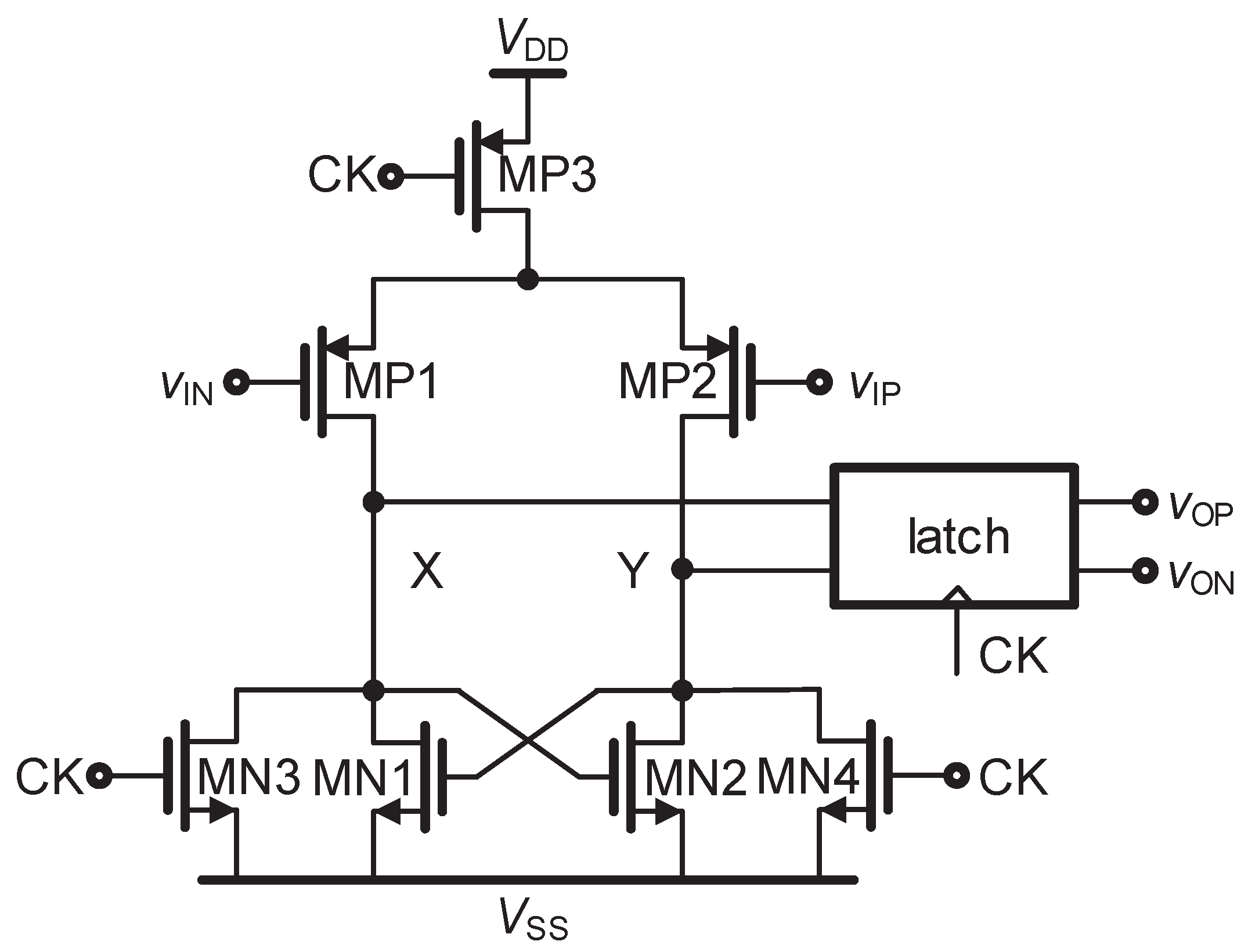
Figure 2.
The equivalent circuit of the comparator.
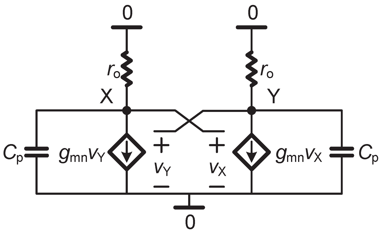
Figure 3.
Delay across common-mode current range.
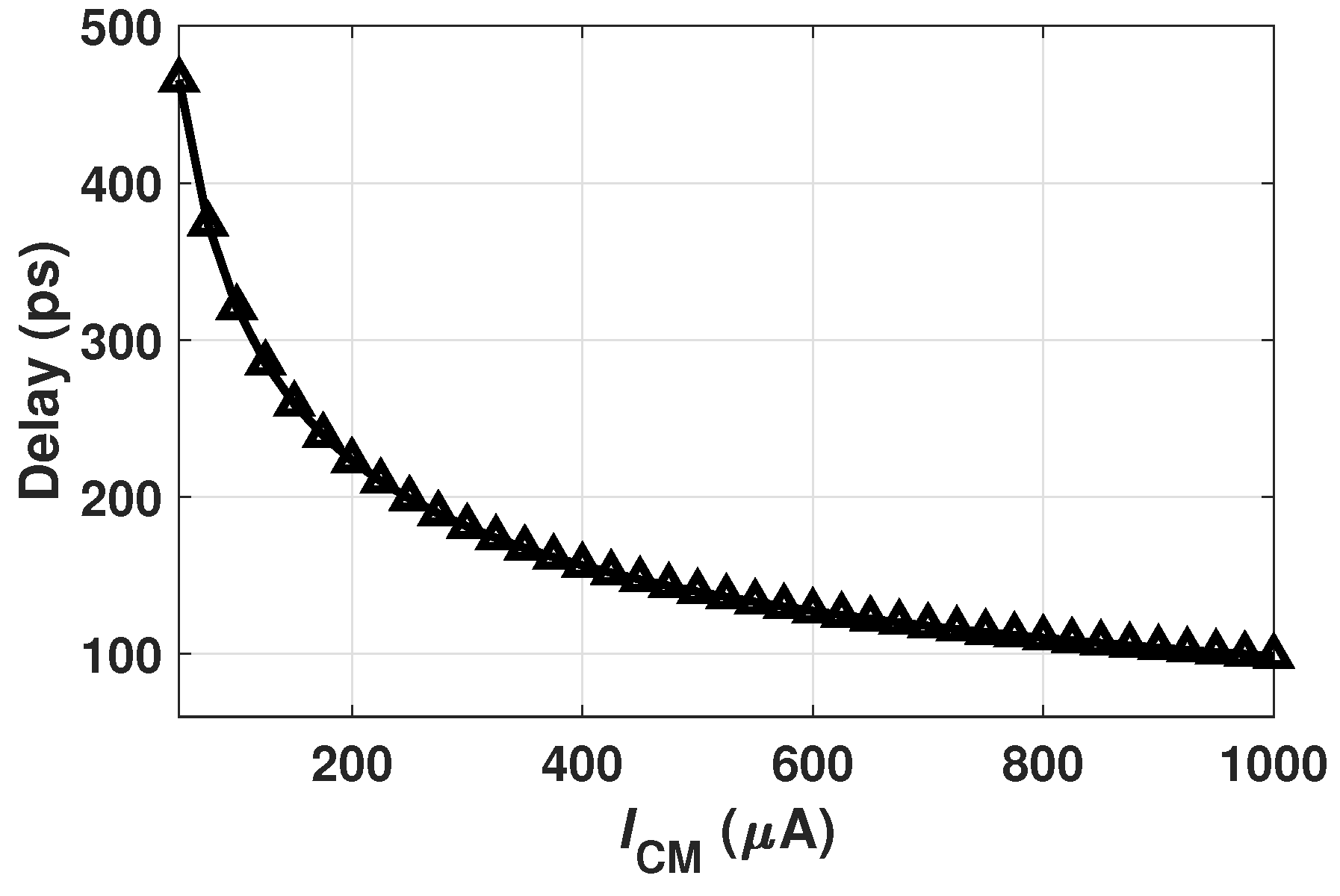
Figure 4.
Proposed enhanced dynamic bias comparator circuit.
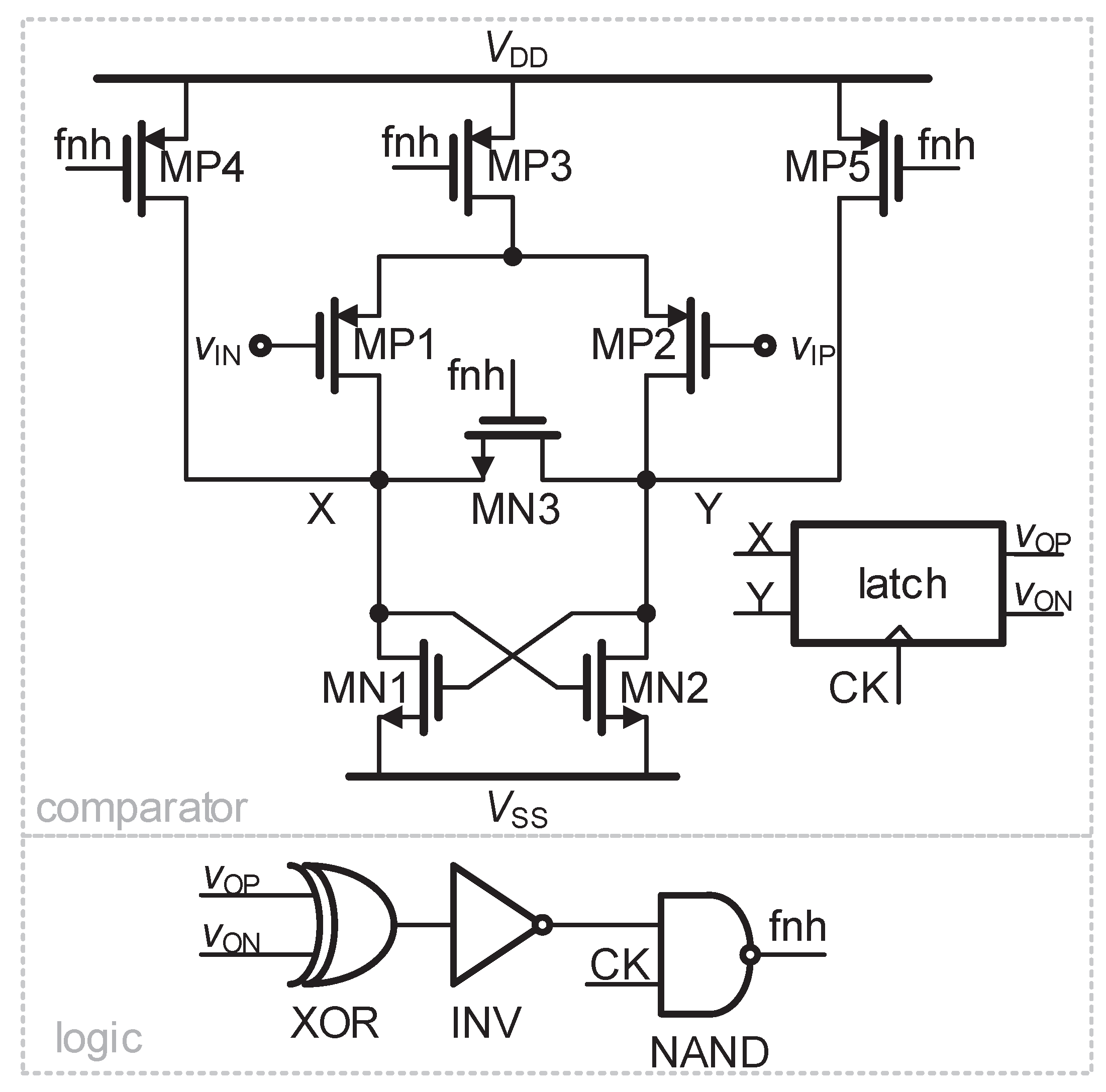
Figure 5.
Operating principle of the comparator with offset: (a) circuit diagram. (b) timing diagram.
Figure 5.
Operating principle of the comparator with offset: (a) circuit diagram. (b) timing diagram.
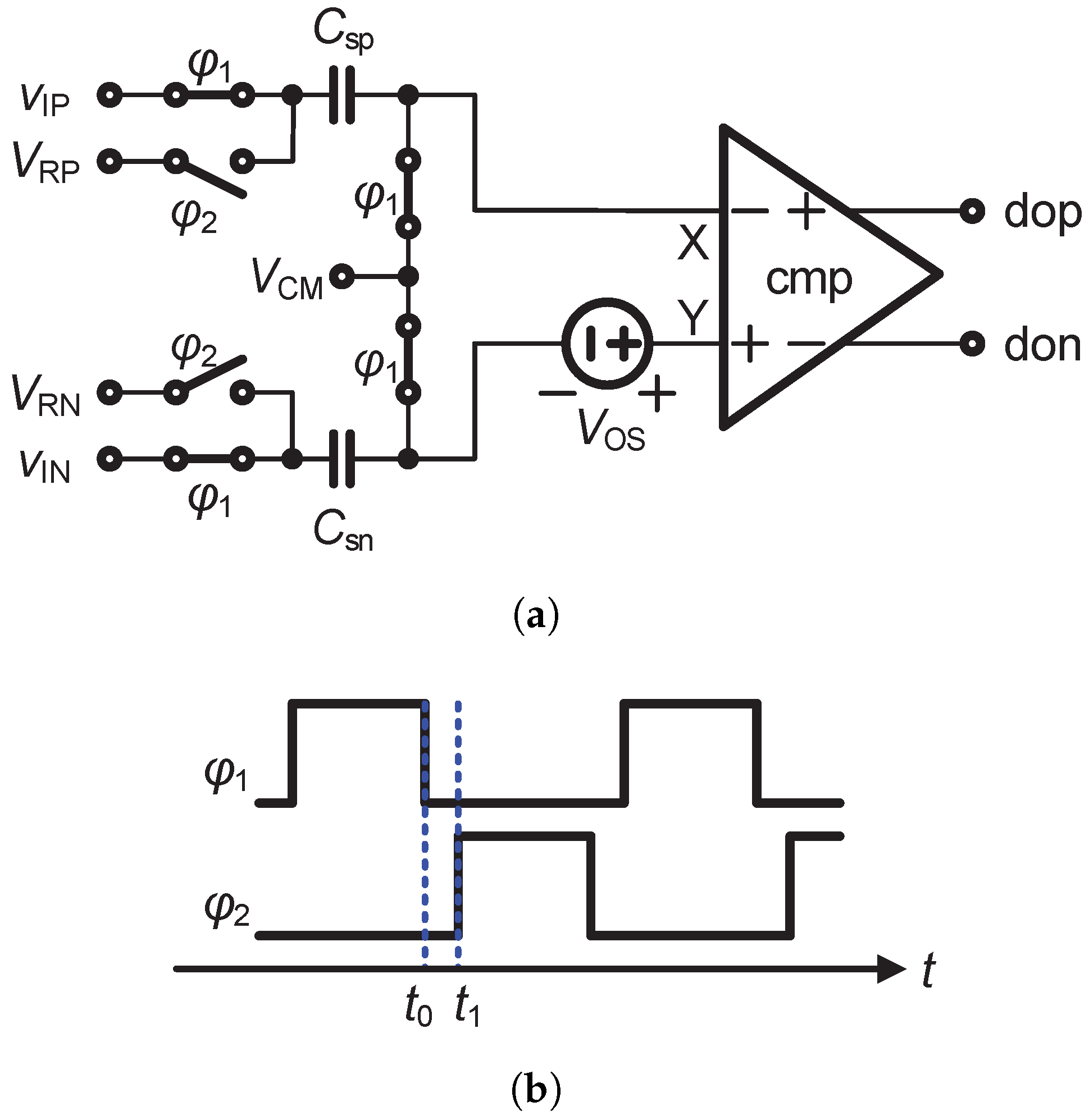
Figure 6.
Operating principle of the comparator with reference-compensated technique.
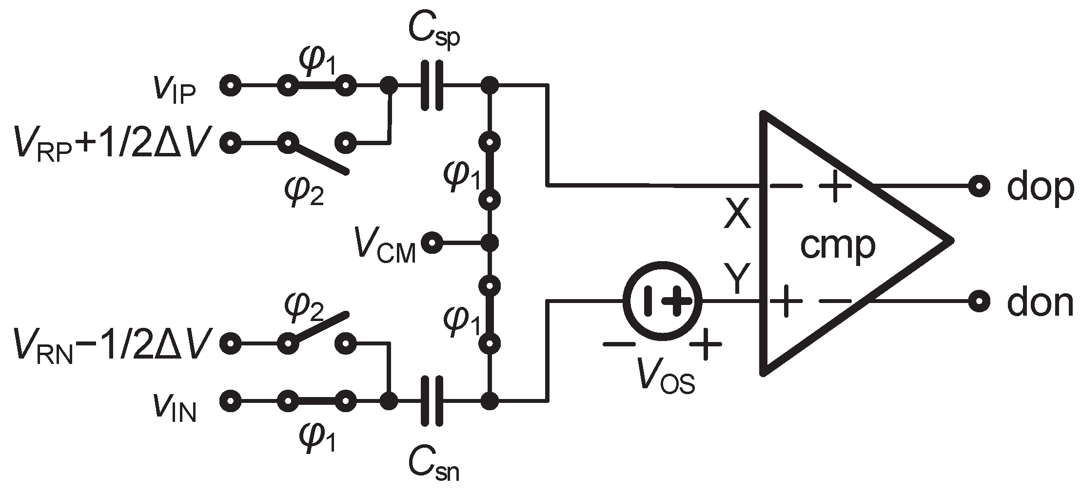
Figure 7.
Schematic diagram of the reference-compensated offset calibration technique.
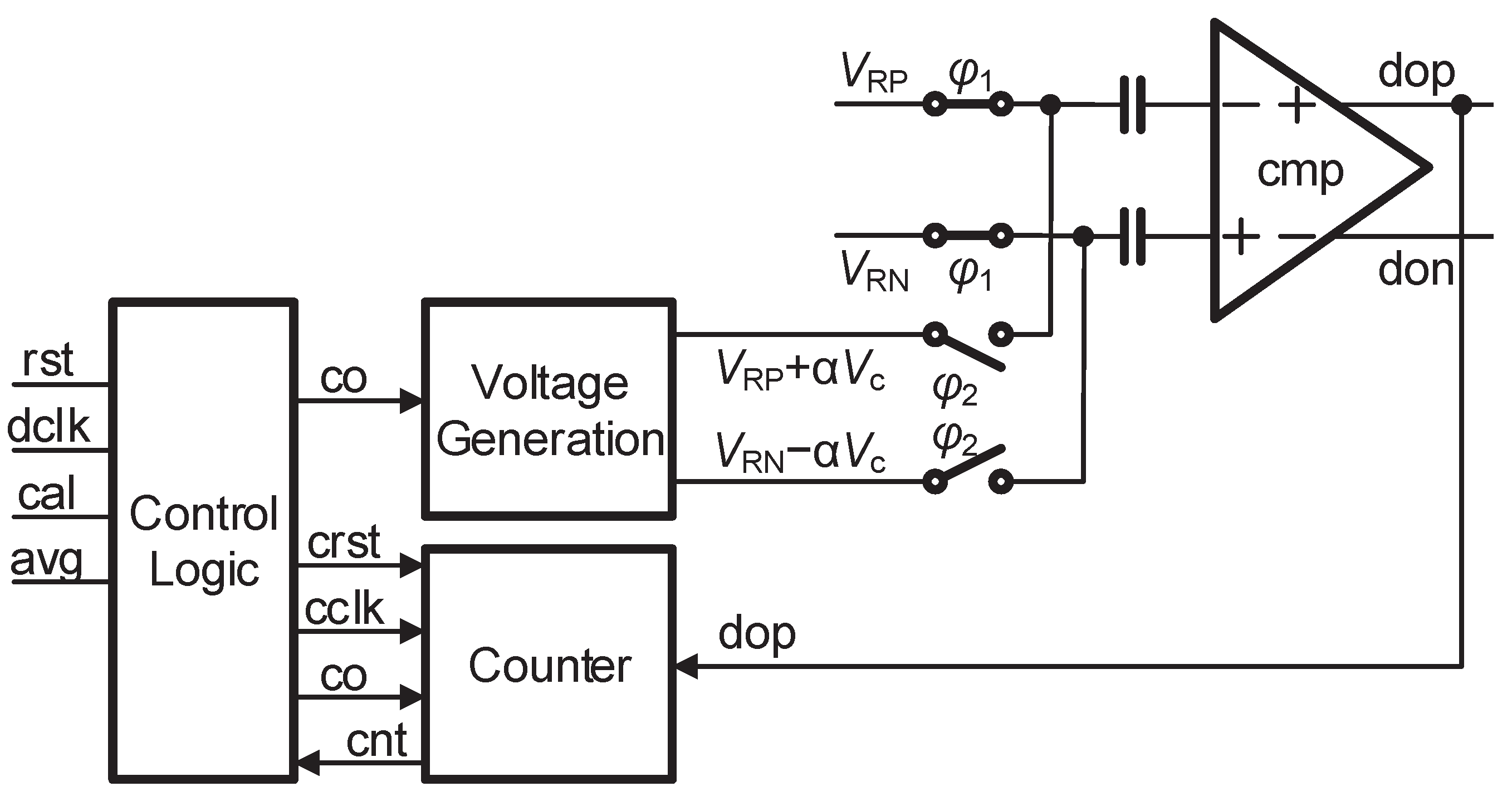
Figure 8.
Typical waveforms of the proposed comparator.
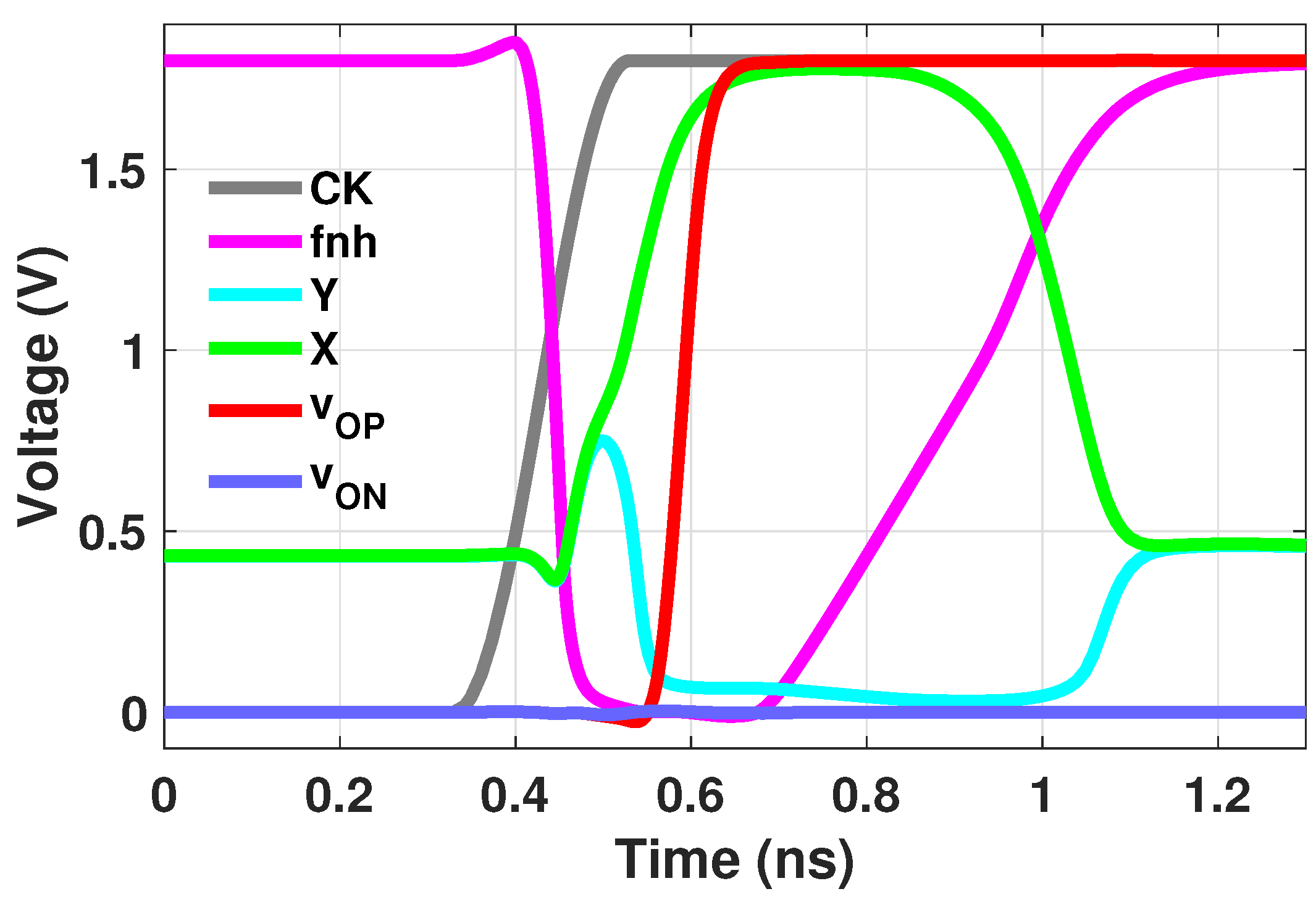
Figure 9.
(a) Simulated delay time and (b) Energy per comparison versus the differential input voltage at the common-mode voltage of 0.9 V.
Figure 9.
(a) Simulated delay time and (b) Energy per comparison versus the differential input voltage at the common-mode voltage of 0.9 V.
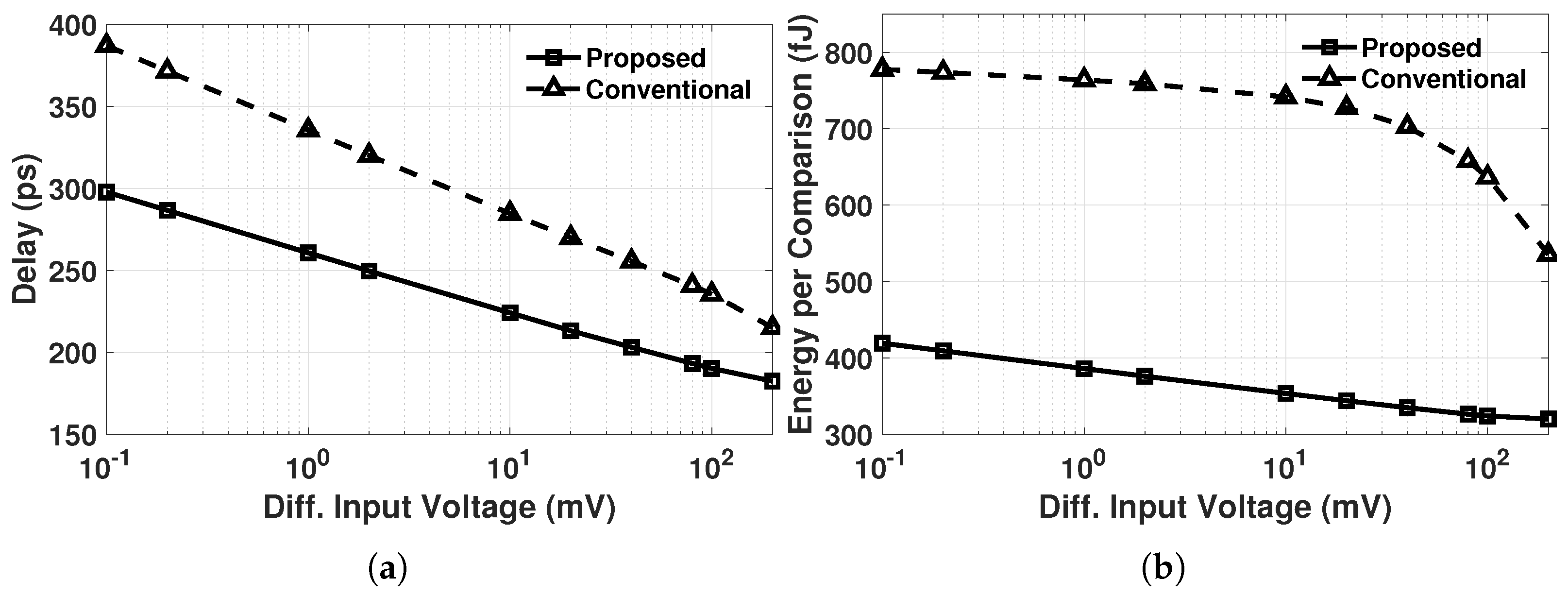
Figure 10.
(a) Simulated delay time and (b) Energy per comparison versus the common-mode voltage at the differential input voltage of 0.1 V.
Figure 10.
(a) Simulated delay time and (b) Energy per comparison versus the common-mode voltage at the differential input voltage of 0.1 V.
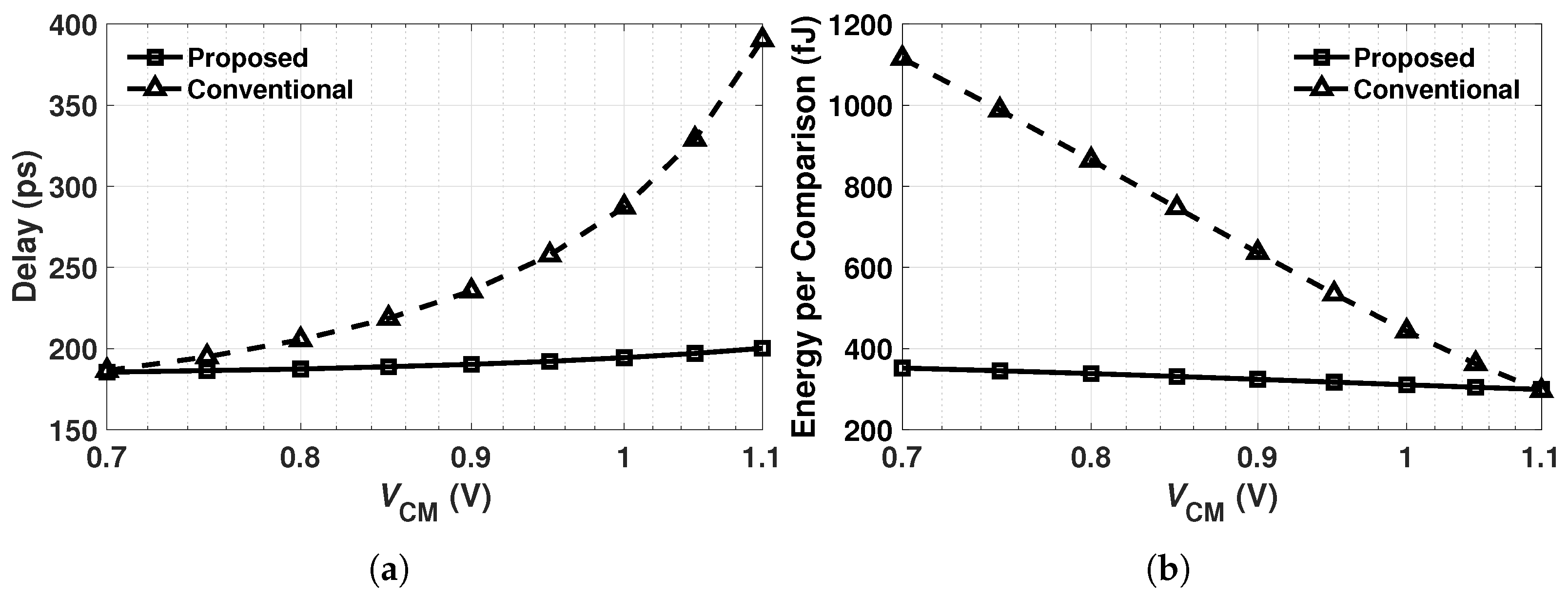
Figure 11.
The histograms of the offset voltage: (a) before calibration. (b) after calibration.
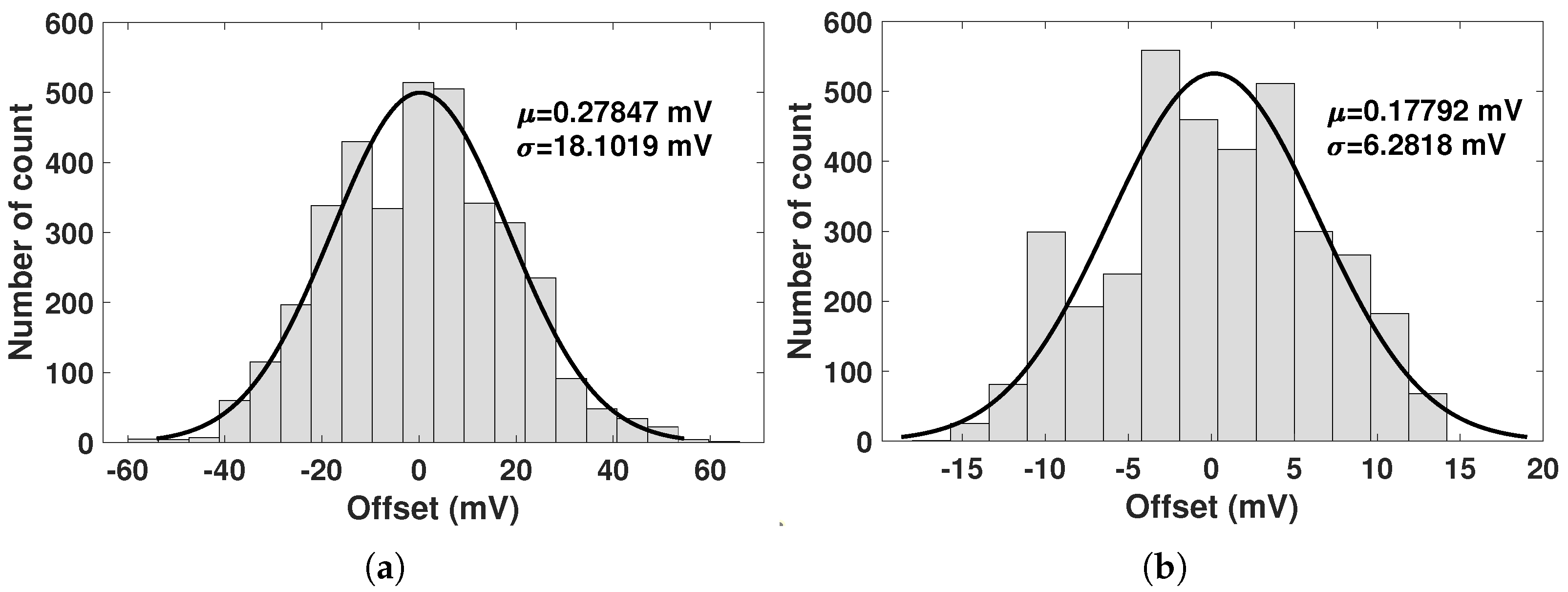
Figure 12.
400-sample Monte Carlo simulation results under TT process.
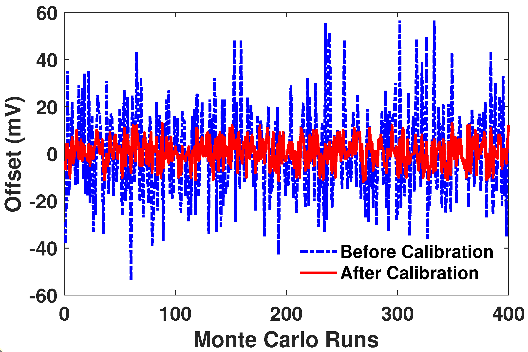

Table 1.
Comparison between the proposed comparator and other comparators.
| This Work | [23] | [24] | [25] | [26] | ||
|---|---|---|---|---|---|---|
| Technology (nm) | 180 | 180 | 180 | 180 | 180 | |
| Supply voltage (V) | 1.8 | 1.2 | 1.2 | 1.8 | 1.8 | |
| Operating frequency (MHz) | 150 | 2150 | 2000 | 500 | 1600 | |
| Delay time (ps) | 190.3 | 550 | 268.6 | 300 | 761 | |
| Energy/comparison (fJ) | 324.2 | 560 | 112.5 | 300 | 418 | |
| Offset voltage (mV) | 6.3 | 7.8 | 7.3 | 2.4 | 3.67 | |
Disclaimer/Publisher’s Note: The statements, opinions and data contained in all publications are solely those of the individual author(s) and contributor(s) and not of MDPI and/or the editor(s). MDPI and/or the editor(s) disclaim responsibility for any injury to people or property resulting from any ideas, methods, instructions or products referred to in the content. |
© 2026 by the authors. Licensee MDPI, Basel, Switzerland. This article is an open access article distributed under the terms and conditions of the Creative Commons Attribution (CC BY) license (http://creativecommons.org/licenses/by/4.0/).
Copyright: This open access article is published under a Creative Commons CC BY 4.0 license, which permit the free download, distribution, and reuse, provided that the author and preprint are cited in any reuse.


