
Submitted:
12 December 2025
Posted:
16 December 2025
You are already at the latest version
Abstract
In-circuit testing (ICT) and functional testing (FCT) are diagnostic methods used to assess the operational integrity of discrete electronic components and circuitry on a Printed Cir-cuit Board (PCB). Commercial electrical testing systems are usually modular, consisting of multiple control and processing circuit boards, which makes them highly specialized and expensive. This creates a significant accessibility challenge, especially for small and me-dium-sized industries. In this study, a low-cost device board was developed to perform in-circuit and functional testing based on fundamental principles of electrical testing. The design incorporates relay banks to connect electrical test node probes with the Device Un-der Test (DUT), enabling resistance and capacitance measurements, shorts and open-circuit detection, voltage stimuli, digital multimeter readings, analog signal condi-tioning and amplification, general-purpose input/output, receive/transmit data, among other functions. These operations are managed via RS-232, opto-isolated UART ports, Ethernet TCP/IP, and digital input/output (I/O) control ports. Prototypes were built and tested in automated functional test setups to verify their performance and proper opera-tion. The results show that a single, low-cost PCB can effectively carry out testing tasks typically performed by expensive commercial systems, providing a versatile and econom-ical alternative tool for electrical testing for prototyping, and end-of-line test equipment.
Keywords:
in-circuit testing (ICT)
; functional testing (FCT)
; printed circuit board (PCB)
; device under test (DUT)
1. Introduction
This paper presents a detailed description of a compact size and cost-effective device board designed to perform in-circuit testing (ICT) and functional testing (FCT) to evaluate the integrity of electronic components and circuitry on a Device Under Test (DUT) [1]. Commonly, the industry adopts these diagnostic methodologies due to defects in the manufacturing process of an electronic product. Defects can arise from various factors, such as improper handling of materials, quality issues in components (e.g., errors in parametric tolerances or internal defects), assembly failures in SMT equipment, or human errors [2]. These systems stand out as indispensable tools, ensuring that manufactured products meet the required electrical specifications and tolerances [3,4].
These systems, developed by leading manufacturers such as Keysight Technologies, Agilent Technologies, Circuit Check, Teradyne, and SPEA, among others, perform electrical testing on the DUT, measuring electrical parameters such as voltage, current, resistance, capacitance, inductance, and short-circuit detection. In summary, these systems convert analog signals to a digital form. In an analog in-circuit test, the PCB undergoes various conditioning stages in which a voltage (V) or current (I) stimulus is applied via interconnections to testing nodes. The response signal is routed through multiplexers and subjected to signal conditioning, including amplification, filtering, and linearization. Finally, an analog signal is digitized and represented as an electrical parameter [1].
The analysis of these highly specialized systems, which offer high precision and reliability in fault detection, reveals a current lack of compact and low-cost alternatives suitable for small- and medium-sized industries. These systems can range from 100 k to 200 k USD, primarily due to system complexity and the need to employ many interconnected modules to perform electrical testing.
Recently, Lai et al. [5] introduced a cost-efficient machine learning model to accurately and efficiently predict resistance, inductance, and capacitance, thereby verifying the integrity and performance of analog IC packages without relying solely on time-consuming testing. Another approach was introduced by Monagas et al. [6]: a modular in-circuit testing system that offers cost-effectiveness benefits for prototype development.
These proposals focus on software implementation and the creation of modular testing systems, similar to in-circuit equipment available on the market. Therefore, the authors in this paper introduce a single, compact, and cost-effective device board capable of performing electrical testing for small- and medium-sized industries, serving as a tool in the electronic design process of an electronic product, and its implementation in automated test equipment, considering the fixture test analysis presented by Oliveira [7].
2. Materials and Methods
2.1. Design Overview
The device board, named the Electrical Testing Board, is shown in Figure 1 and consists of a single PCB. It is capable of interconnecting the test probe nodes of a DUT through the device board edge connector, also called gold finger connector for multiple automated analog in-circuit testing tasks, such as resistance and capacitance measurements, short-circuit detection and opens, as well as functional tests including voltage stimuli, digital multimeter measurements, analog signal amplification, audio detection, and data transmission/reception. Electrical schematics are shown in the Appendix Section.
The device board performs testing tasks via direct connectivity between the DUT test nodes and its edge connector. A general design overview is shown in a block diagram in Figure 2; every block module can be interconnected to perform a specific task.
A detailed description of the 88 gold fingers on the device board edge connector is shown in Figure 3. A direct connectivity with the power management module is linked, which is integrated by the power supplies inputs to power-up the device board (e.g., +15 V, and -15 V), and obtaining the power supply outputs (e.g., +5 V, and +3.3 V) by the low-dropout voltage regulators to power-up device board integrated circuits, analog voltages for power management, signal conditioning, and analog voltage stimuli stages.
The device board establishes direct connectivity to the DUT via sixteen available testing nodes, which can be connected or overlapped to any of the four via buses to interact with in-circuit and functional testing modules. This connectivity is achieved via a matrix array of relay banks on four via buses (M+, M-, V+, and G-) controlled by two slave MCUs, which provide via-bus connectivity.
The main MCU provides direct control of the testing modules via general-purpose input/output (GPIO), I2C, and SPI. Additionally, a direct connection to six optional digital inputs/outputs, two digital inputs/outputs for the monitoring and control of the device board: (i) a digital input for board-selection, and (ii) a digital output for board-busy status.
The slave MCUs monitor six general high-voltage inputs to a low-voltage transition, eight general relay outputs with high-current capability for multiple purposes, and three optional digital inputs/outputs.
The edge connector also includes two opto-isolated UART buses, one I2C bus, eleven multiplexed GPIO to the M+ bus, denoted as ‘Address’, and two direct finger contacts to the M+ and M- buses.
A detailed description of the design circuitry involved for each gold-finger connectivity is provided in the following sections.
2.1.1. Communication Approach
Device board capable of being controlled via communication RS-232, opto-isolated UART buses, and Ethernet TCP/IP. Figure 4 shows the circuit design for interacting with a master device (e.g., a computer, PLC, etc.) via instructions or commands to perform a specific task, such as sending tolerances, measurement limits, starting a testing task, requesting testing results, or even controlling different testing blocks via software.
Two opto-isolated UART circuits capable of protecting the MCU UART ports from any collision issues due to any potential malfunction over the UART bus. This solution effectively manages a unique COM port on a master device to control multiple device boards in parallel, which are directly connected via the edge connector. It enables parallel testing in a fixture with multiple DUTs, using a single digital input on each testing device board to indicate the board-selection status for each instruction. Another communication approach is the Ethernet module with a Microchip LAN8720, a single-chip Ethernet physical layer transceiver (PHY), which enables direct control of the device board via TCP/IP commands. A helpful solution when the device board needs to be controlled directly via a PLC or an intranet network, without a computer. Additionally, a DB9 connector with RS-232 communication is added for technical purposes, such as debugging and diagnostic tasks. To establish communication between the device board and the master device, a trustworthy communication frame is developed. Commands and parameters can be sent to the device board for interpretation and execution, as shown in the frame packet in Figure 5.
The frame packet is delimited between a start 1-byte denoted by the open bracket symbol ‘{‘ and a stop 1-byte by the close bracket symbol ‘}’. The command type is 1-byte data size; 255 operative tasks. Some typical command examples are
- 0 × 01: Start an automated testing task.
- 0 × 02: Send data limits.
- 0 × 03: Request data results.
- 0 × 21: Write general relays
- 0 × 22: Read general inputs
- 0 × 50 to 0xAF: Start individual testing tasks.
After a command is given, optative data can be sent as additional parameters. It can process any known data representation, such as char, integer, and string, by converting their hex-format values to ASCII representations, and floating-point data types to their IEEE Standard 754 hex-format values [8]. Note: when multiple data items are sent, each must be separated by a comma ‘,’ to process them in order. Examples of data types are shown in Table 1.
A crucial part of communication is ensuring that what is sent is interpreted correctly. To handle this, the data packet includes a 2-byte checksum variable. This variable performs a Boolean summing for each byte in-process and stores the value to be sent for comparison with the checksum calculated by the master device based on what the device board received. Figure 6 shows an example of a data frame packet for a single testing task: measuring an analog voltage in selected test nodes with some random limit parameters.
2.1.2. Relay Banks
Relay banks are an essential part of the testing device, connecting the DUT’s test nodes to multiple integrated testing modules via V+, M+, M−, and G− buses, each with its own relay banks. These buses enable a compact device design that can interconnect buses to any circuitry required for testing, offering a versatile solution.
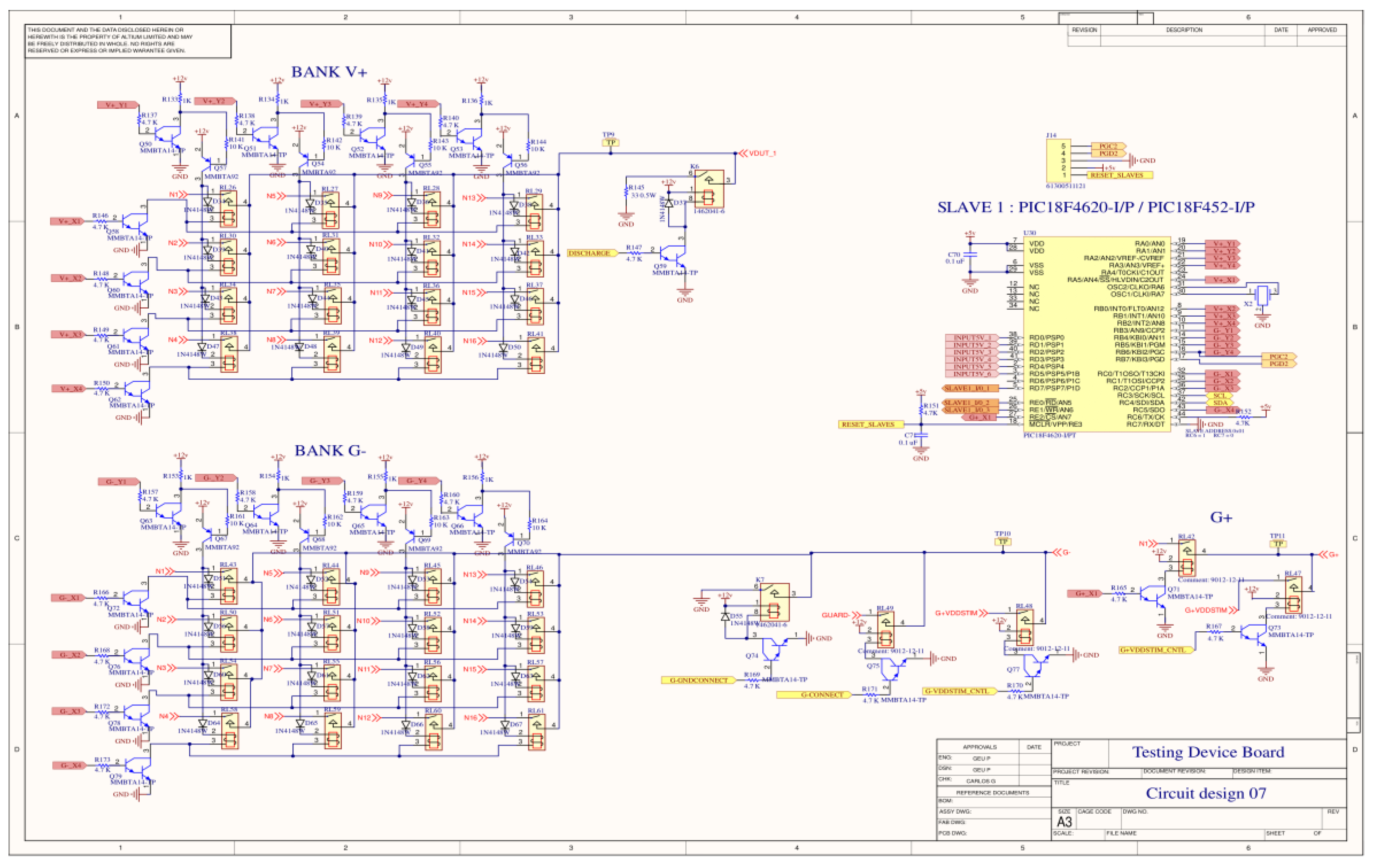
The V+ bus interconnects a high-current power supply to the DUT and supports optional discharging processes. The M+ and M− buses are closely related; they interconnect multiple functional blocks to perform a range of testing tasks, including voltage stimuli, digital multimeter measurements, analog signal amplification, audio detection, short-circuit detection, and open-circuit testing, among others. The G-bus interconnects the DUT test nodes to ground, guard circuitry, and sets up the ammeter circuitry.
Figure 7 provides an overview of the relay bank for the G-bus, configured as an X-Y matrix controlled by a slave MCU via GPIO pins. This matrix includes 16 test nodes. Note: another relay bank’s buses use an identical X,Y matrix.
2.1.3. Programmable Power Supplies
A compact, programmable power supply with a 12-bit voltage-output digital-to-analog converter (DAC), a pre-regulator circuitry, and overcurrent protection to provide stable analog voltages capable of interconnecting voltage stimulus in the V+ and M+ buses.
Figure 8.
Programmable power supply circuit.
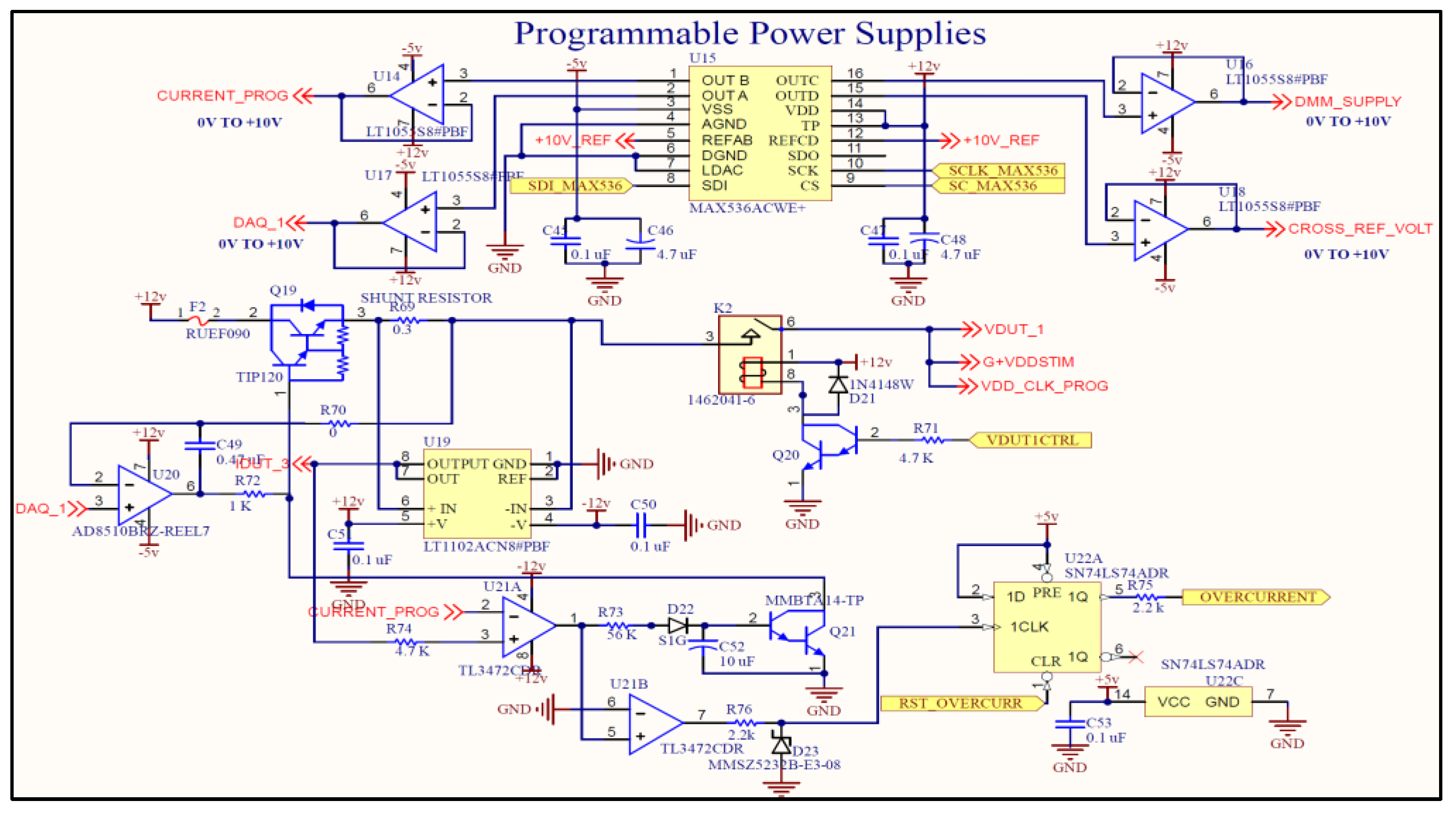
- DAQ_1: A high-accuracy, stability, and precision analog voltage capable of setting a high-current power supply (VDUT) from 0 V to 10 V through a pre-regulator circuitry and overcurrent protection circuitry, current is controlled and monitored by the main MCU. This power supply can be connected to the V+ bus and serves as the primary voltage stimulus source for the DUT.
- DMM_Supply: A high-current power supply from 0 V to 10 V via a pre-regulator circuitry able to be connected to the M+ bus for general voltage stimuli for testing tasks.
- CROSS_REF_VOLT: An analog voltage that can be set as a reference voltage for analog comparators, pull-ups, and speed-up circuitry in M+ and M- buses.
- CURRENT_PROG: An analog voltage used to set an analog current limit in the overcurrent protection circuitry in the DAQ_1.
A practical use of the V+ bus is the optional relay for electrical discharging of the DUT through a low-value, high-wattage resistor, as shown in Figure 9. This is typically used when electrical discharging is necessary.
2.1.4. Programmable Pull-Ups, Pull-Downs, and Analog Comparators
A functional module connected to the M+ and M- buses includes programmable pull-ups and pull-downs, as shown in Figure 10. These are designed to tie a high or low logical voltage as needed for testing purposes. Pull-ups can be set to a programmable voltage level using Cross Reference Voltage or 5 V in the M+ bus, and two pull-downs in the M- bus to different resistance values to ground.
Another practical use in the pull-downs section is the named Guard-connection, which is connected via relay access to the G-bus and, consequently, to any test node in the DUT. This setup is ideal when a test measurement depends on other test nodes or even for guarding protection.
On the other hand, M+ and M- buses share a programmable analog-comparator module capable of performing testing tasks, such as short-circuit and open-circuit detection. This module interacts with the programmable power supply to set a cross-reference analog voltage at the comparators’ inputs. It is ideal for high-speed short- and open-detection using a stimulus voltage applied to a particular test node on the V+ bus, and for measuring its response from another test node set on the M+ or M- buses.
2.1.5. DMM
A digital multimeter (DMM) designed to measure analog voltage and current in a DUT by interconnecting test nodes to M+, using an external 16-bit Analog-to-Digital Converter (ADC) or the optional 10-bit MCU-based ADC. Voltmeter ranges are relay-selectable, from 0 to 10 V and 0 to 100 V, as shown in Figure 11.
The functional ammeter is based on a transimpedance amplifier circuit that converts current into a proportional voltage via a forward-biased signal diode (Vforward), as shown in Figure 11. The ammeter ranges are defined by three amplified scale settings, which the authors have carefully characterized to ensure a linear voltage vs current response. The ammeter operates directly with the G− and V+ buses to produce a voltage response that can be measured in the M+ bus.
Another approach is to measure resistance and capacitance using a combination of functional modules on the V+, M+, and M- buses to determine the electrical parameters. For example, to measure the electrical resistance of a DUT, the estimation is based on a voltage divider between the nodes in V+ and M- buses, and the M+ bus to measure the voltage between nodes, as shown in Figure 12.
A voltage divider is configured on the device board using the functional module pull-downs and the voltage stimuli module, which includes reference resistances (named Rref in this section) to set the unknown resistance Rx of the DUT. A reference voltage is applied to the voltage divider in the V+ bus, generating an output voltage that can be measured at the circuit nodes in V+ and M+. The voltage divider relationship is given by Equation (1),
where Vout is the voltage measured at the nodes, and Vin is the applied input voltage from the +V bus, rearranging Equation (1) allows for solving the unknown resistance Rx using these measured voltages and the known reference resistance. Specifically, the unknown resistance is calculated through the voltage divider formula. This approach enables easy implementation, precise estimation of the component’s resistance using voltage measurements, and the delivery of accurate, reliable results.
Another approach is to measure the electrical capacitance of a component using direct sensor–microcontroller interface circuits, or Direct Interface Circuits (DICs) [9,10], which are categorized into charge-time-based [11,12,13,14] and discharge-time-based [15,16] circuits. Both rely on RC configurations to estimate resistance and capacitance, as shown in Figure 13.
The operation relies on measuring the time interval required to charge (Tc) or discharge (Td) the capacitor Cx through the resistive element R, until a voltage threshold is reached, either the upper threshold VTH or the lower threshold VTL, depending on the operation mode. This time interval serves as the basis for estimating capacitance.
The capacitance is directly proportional to the measured time interval. Consequently, the measurement process is executed in two distinct stages: charging and discharging of the capacitor Cx. Table 2 summarizes this process, detailing the digital pin states and the intervals required to complete each stage.
Figure 14 shows an scheme to estimate capacitance in the device board, which is achieved by following next steps: i) charging capacitor via V+ bus in Node 1 at the voltage stimuli VDUT and interconnecting M- bus to the comparator module, and ii) start simultaneously the embedded timer and a discharge-time-based process by setting up the pull-down resistor Rpull-down in the M- bus.
The comparator output stops the embedded timer in the main MCU when the capacitor voltage reaches the cross-reference voltage VCROSS REF, serving as a comparator threshold to stop the embedded timer and estimate capacitance, solving (2) in terms of the capacitance Cx.
2.1.6. Signal Amplification, Audio Conditioning, and Multiplexing
Device board capable of amplifying small amplitude signals from the DUT via direct connectivity to the test nodes via the M-bus with a selectable relay, as shown in Figure 15. A non-inverting amplifier circuit with a programmable gain circuitry through a digital potentiometer via I2C communication. Also, an audio conditioning circuitry able to process audio to an analog level for analysis of amplitude or frequency ratio. The resulting signals are connected to the M+ bus via a multiplexer IC for measurement by the DMM module. The multiplexer also includes eleven multiplexed GPIO ports that can be directly connected to the device board edge connector for testing.
2.1.7. General Opto-Isolated Inputs, Speed-Up Signal, and EEPROM
Figure 16 shows the circuit design for connecting an analog voltage to an opto-isolated circuit on the M+ and M- buses to detect voltage transitions without direct wiring to the device board circuitry. This setup is proper for functional purposes when a DUT signal should not interact with external devices.
Additionally, a speed-up circuit capable of generating an M-bus Pulse Width Modulation (PWM) output signal with an adjustable duty cycle for testing purposes, and a 2 K-bit Electrically Erasable Programmable Read-Only Memory (EEPROM) able to store parametric data, such as calibration factors on the device board, test results, and relevant testing information via I2C with the main MCU.
2.1.8. General-Purpose Inputs/Outputs
The device board can control eight general relay outputs with high current capability, ranging from 500 mA to 2 A between relay contacts. Additionally, the device board can translate high-voltage general-purpose inputs to a low-voltage level, preventing them from affecting the MCU’s digital voltage levels, which is helpful for monitoring peripherals, such as sensors. Figure 17 shows both approaches.
2.2. Implementation Overview
The device board is implemented in automated test equipment capable of performing end-of-line functional parallel testing. This approach is achieved by using a test fixture with eight nests for the DUTs, each nest requiring a device board, which allows a parallel test sequence, as shown in Figure 18.
2.2.1. Control
Device board control is achieved via RS-232 communication with a computer acting as the master device. It uses its native COM1 port to convert RS-232 to UART, providing direct connectivity to the eight device boards in parallel wiring at the opto-isolated UART module in the gold-finger connector. A PCI-6320 card from National Instruments (NI) is used in the computer to control the digital output for the board-selection input and monitor the digital input from the output board-busy status.
- Board-selection. A digital input indicates a direct selection of a specific device board to accept any RS-232 instruction given.
- Board-busy. A digital output indicates its busy status to the master device.
The master device controls multiple testing device boards via digital output selection. This control is considered an access control because all device boards receive any data packets sent by the master device to execute testing tasks via RS-232 communication on port COM1. Figure 19 presents a general control process flow to control a single device board to perform an automated testing task.
A detailed description of the process flow to control the device board and data packets sent by the master device to perform an automated testing task is explained as follows:
- Device board selection. The master device indicates a low-to-high digital output transition via the PCI-6320 to select a specific testing device board.
- Communication process. (i) The master device sends parameters such as the model name to test, test limits and tolerances, test node setup, and specific electrical tests to perform, and (ii) the master device sends a test command to start an automated testing routine based on the previously received testing data.
- Device board Busy-Status. After the test command is issued, the device board initiates a low-to-high transition on its digital output to indicate a busy status to the master device. The master device runs in a while loop, waiting until the testing device board completes a testing routine and transitions the busy state from high to low; this change indicates that the testing task has finished.
- Request Results. At this point, the master device can request the testing results by sending a request-result data packet.
Every instruction on each device board is executed in a repetitive loop in the master device at 115,200 bps, enabling a fast sequence to perform testing tasks according to the master device’s instructions.
2.2.2. Testing Tasks
The device board follows the testing tasks required by the DUT, as the automated test equipment is part of an end-of-line process, meaning it is the last chance to validate functionality in the manufacturing process of an electronic product before packing. Some individual testing tasks are listed below:
- Short-circuit and open-circuit testing. Correct wiring assemblies.
- Voltage stimuli to the DUT and monitor responses from signal processing.
- Voltmeter measurements, and ammeter to standby-current measurements.
- Resistance and capacitance measurements.
- Read analog and digital signals.
- Audio detection.
- Read and write DUT data via UART. Factory-stored parameters in the product.
- Mix signals input and outputs depending on functional testing in the DUT.
Some testing tasks can vary depending on the DUT requirements, where relay banks enable multiple configurations for functional and in-circuit testing.
3. Results
3.1. Experimental Evaluation
The experimental evaluation is based on the functional validation of the hardware/software of the low-cost device board shown in Figure 20 and its implementation in an automated test equipment capable of performing end-of-line functional parallel testing with eight testing boards.
In this study, a graphical user interface was developed using the LabWindows/CVI development platform, enabling direct communication with the testing device board via the RS-232 connector to control and validate its individual modules during in-circuit and functional testing. Figure 21 shows the user interface and a power-up hardware box for direct access to the device board for validation and debugging.
The device board validation begins by checking the programmable power supplies’ stability across different voltage ranges with a resistor load, and the proper functionality of the relay banks, including measuring resistance between relay contacts, short detection, and open detection between nodes. Another test includes verifying the functionality of analog comparators, the signal conditioning module, audio detection, pull-ups, pull-downs, opto-isolated UART communication, general inputs, and general relays. The user interface comprises practical validation of in-circuit measurements, including ohmmeter, capacitance, voltmeter, and ammeter testing capabilities, with direct access to the device board for debugging.
3.1.1. Communication Approach
Communication is validated directly via a master device, in this case, a computer that sends data packets via the opto-isolated UART ports, the RS-232 connector, and the Ethernet TCP/IP interface to receive/transmit data. The opto-isolated UART ports and RS-232 connector were evaluated by sending simultaneous data packets to the test device at 115,200 bps, ensuring proper data processing via UART. On the other hand, Ethernet capabilities were evaluated, establishing a direct connection between the device board and the local intranet, enabling remote access via the assigned IP address. Every communication approach allows direct control of the device and the sending of data packets to multiple testing tasks, depending on the programmer’s approach.
3.1.2. Programmable Power Supplies
The device board can supply four programmable power supplies: one for current monitoring, one for cross-reference voltage, and two for voltage stimuli. The evaluation focused on the power supplies for voltage stimuli for DAQ_1 and DMM_Supply, ranging from 0 V to 10 V, with a voltage accuracy of 3.2 mV and high current capability up to 1 A via a pre-regulator circuit design. An overcurrent protection circuit was evaluated using the programmable CURRENT_PROG to set a current limit, ensuring software-controlled current protection across different ranges. The CROSS_REF_VOLT sets a reference voltage with high-voltage stability across involved modules.
3.1.3. Programmable Pull-Ups, Pull-Downs, and Analog Comparators
Programmable pull-ups, pull-downs, and analog comparators were evaluated internally using the device board hardware box, as shown previously in Figure 21, which allows direct connections between buses and voltmeter measurements. These circuit modules are designed for in-circuit testing, including open-circuit and short-circuit detection and signal conditioning, making them an inexpensive and fast testing solution.
3.1.4. DMM
Voltmeter and ammeter measurements were evaluated in real time or continuously using the device board hardware box and the graphical user interface. The voltmeter accuracy is around ±150 µV for input voltages from 0 V to 10 V and ±2.1 mV for input voltages from 0 V to 100 V. Ammeter ranges are given by the three-scale ammeter ranges, the evaluated scale ranges allowed current measurement from; (i) 1 µA to 10 µA with a accuracy of ±0.02 µA, (ii) 10 µA to 100 µA with a accuracy of ±0.1 µA, and (iii) 0.1 mA to 1 mA with a accuracy of ±2.1 µA. These three-scale ranges are adjustable based on DUT requirements, and the current ranges can be changed to expand ammeter measurements.
Ohmmeter and capacitance measurements were also evaluated using the device board hardware box and the user interface to validate in-circuit measurements. Device board evaluation demonstrated resistance ranges from 0.5 Ω to 1 MΩ with three accuracy ranges observed: (i) 1% accuracy for ranges of 0.5 Ω to 10 kΩ, (ii) 4% accuracy for ranges of 10 kΩ to 100 kΩ, and (iii) 8% accuracy for ranges of 100 kΩ to 1 MΩ., and capacitance measurement ranges from 10 nF to 220 µF, with two accuracy ranges: (i) 7% for 10 nF to 10 µF, and (ii) 12% for 10 µF to 220 µF.
3.1.5. Signal Amplification, Audio Conditioning, and Multiplexing
All these signals in the amplitude domain were evaluated using the device board hardware box connected to the buses to process analog signals for amplification, audio conditioning, and multiplexing them to test nodes.
An evaluation was performed on an analog amplitude-domain signal at 0.5 V, amplified by factors of 2, 4, and 6 per the design circuitry, and the resulting output was measured with the voltmeter module. According to the audio circuit conditioning, a signal pattern voice was processed and amplified to convert it to a digital, discrete format, enabling the processing of audio patterns for testing purposes, such as voice and pattern recognition integrity.
3.1.6. General Opto-Isolated Inputs, Speed-Up Signal, and EEPROM
The general opto-isolated input circuit was evaluated using the device board hardware box with an external high-voltage input, which does not interact with the device board; it proved a helpful tool when an external signal could damage the device board, or even when the grounding circuit cannot interact simultaneously.
Additionally, an output PWM speed-up signal with an adjustable duty cycle was evaluated and measured with an external oscilloscope; the duty cycle is determined by the main MCU oscillator, which can be configured to operate from 8 MHz to 80 MHz. The MCU controls the ON and OFF periods of the PWM signal. Finally, a simple EEPROM evaluation was performed by sending data from the computer to store the test limits and reading them back to ensure data allocation. This EEPROM is useful for storing parametric data or offset calibration data.
3.1.7. General-Purpose Inputs/Outputs
General-purpose inputs and outputs were evaluated using the device board hardware box with interconnected voltage stimuli to general inputs and general output activation at relay contacts. Relay contacts were tested for open-circuit and resistance measurements between contacts to ensure proper functionality.
3.2. Automated Device Board Implementation
The device board is implemented in an automated test equipment capable of performing end-of-line functional parallel testing with eight device boards. Figure 22 shows a general overview of the test equipment.
The eight-device board interacts with each DUT individually. This means that each device board controls a DUT via the 88 gold-finger edge connectors to the test nodes (pogo pins) on a fixture plate. To execute parallel electrical testing, the fixture is indexed to a DUT grid pallet where DUTs are placed at each nest.
The specific test plan for the DUT is confidential, as it is a genuine manufacturing product running in an industrial factory; in this case, a general test plan can be provided, which is performed by the testing device board:
- Power up the DUT and read data via UART communication.
- Correct wiring of mechanical connectors via voltage stimuli and open circuit testing.
- Battery voltage measurement with and without load.
- Standby-current measurements.
- Press mechanical buttons and measure voltage responses in specific test nodes.
- Battery bars presence, short circuit detection in assembly bars.
- Audio detection and sound patterns.
4. Conclusions
This paper presents a compact, low-cost, and efficient test board for in-circuit testing (ICT) and functional testing (FCT) of electronic devices. Key contributions include the design of a testing device built on a single PCB that enables a broad range of measurements and tests, including short-circuit and open-circuit detection, resistance and capacitance measurements, voltage stimuli, analog signal amplification, audio detection, and data communication. The device board fabrication cost is around 700 USD, a cost-effective solution for testing, as its easy integration into an automated test setup capable of parallel testing up to eight Devices Under Test (DUTs) demonstrates a versatile, economical solution, particularly suited for small- and medium-sized industries that require practical quality control tools during the manufacturing process or prototype development.
Experimental results validate the device’s functionality and proper operation, positioning it as an accessible alternative to complex, costly commercial systems and facilitating the adoption of sophisticated electrical testing in budget-constrained industrial environments. Future research opportunities lie in integrating testing techniques with machine learning principles to optimize testing time and enable faster fault detection, and to increase testing coverage by leveraging more testing node capabilities.
Author Contributions
Conceptualization, G.M.P.-C. and E.S.; methodology, G.M.P.-C., E.S., J.M. and J.M.; writing—original draft preparation, G.M.P.-C.; writing—review and editing, E.S., J.M., F.E.-A., G.B. and A.H.Á.; supervision, E.S. and J.M. All authors have read and agreed to the published version of the manuscript.
Funding
This research was funded in part by the SECIHTI and UACJ.
Data Availability Statement
The original contributions presented in this study are included in the article. Further inquiries can be directed to the corresponding author.
Conflicts of Interest
The authors declare no conflicts of interest.
Appendix A. Electrical Design Schematics
Figure A1.
Circuit design: main MCU, communication ports, and edge connector interface.
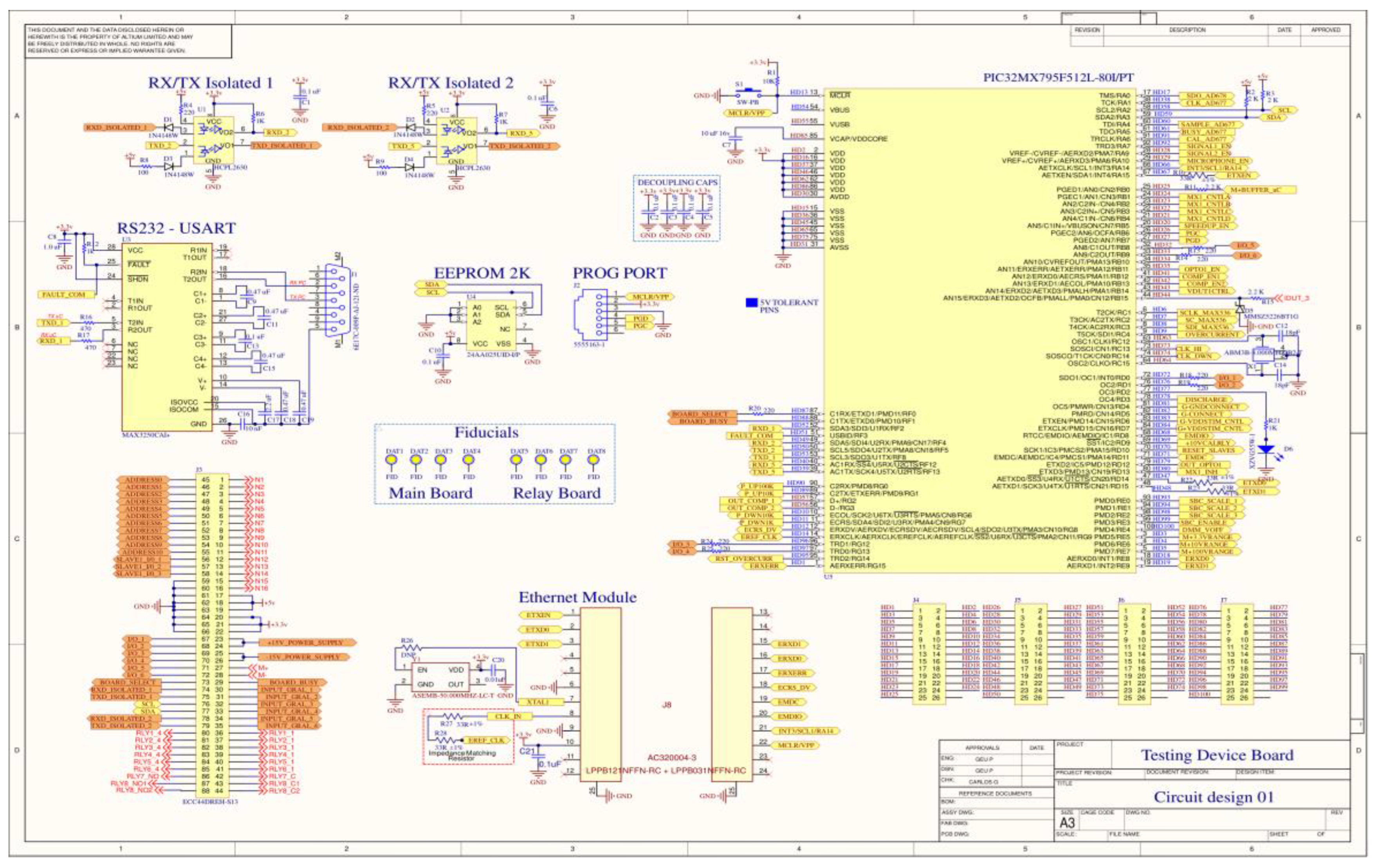
Figure A2.
Circuit design: DMM, pull-ups, pull-downs, and analog comparators.
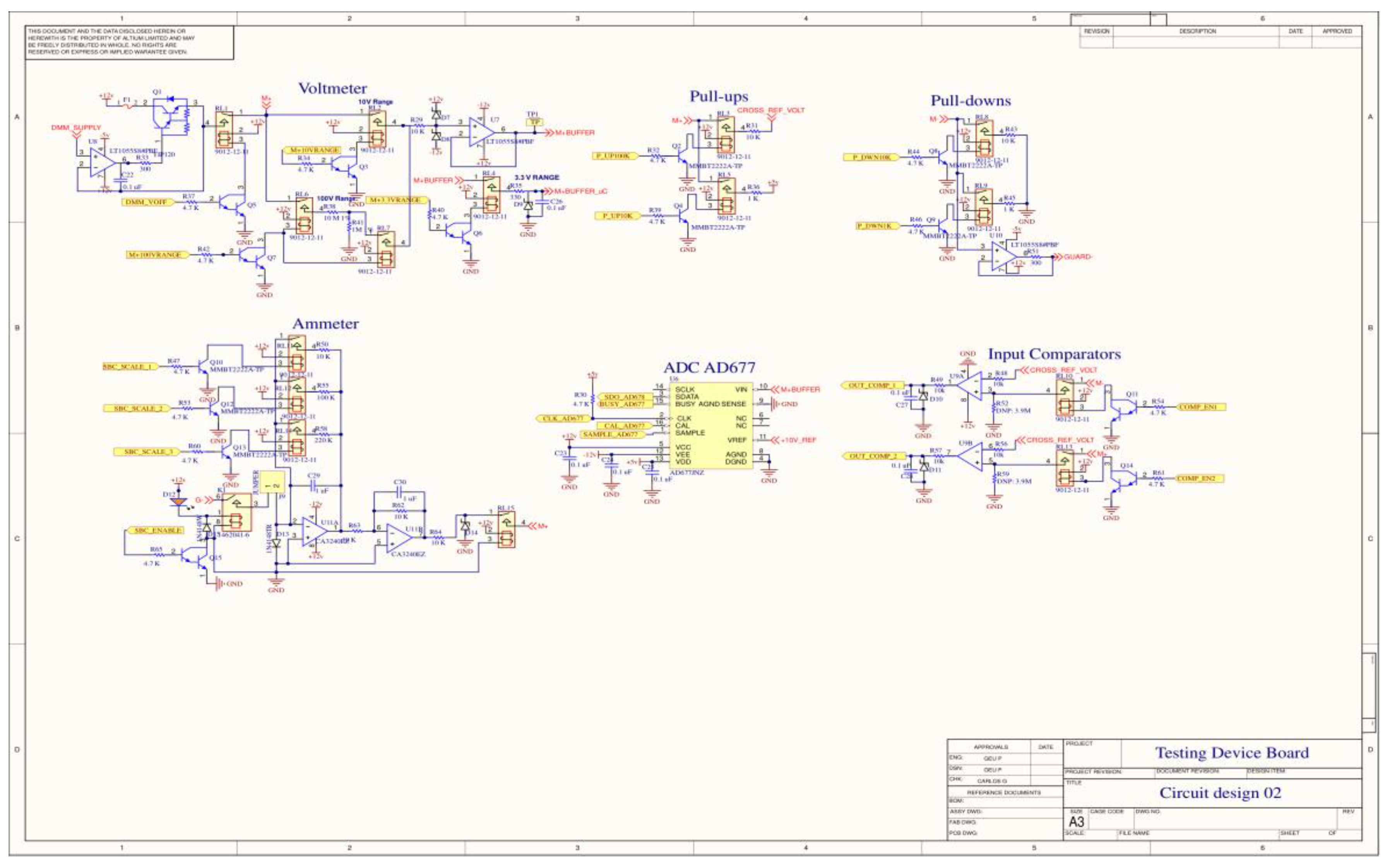
Figure A3.
Circuit design: Programmable power supplies and voltage regulators.
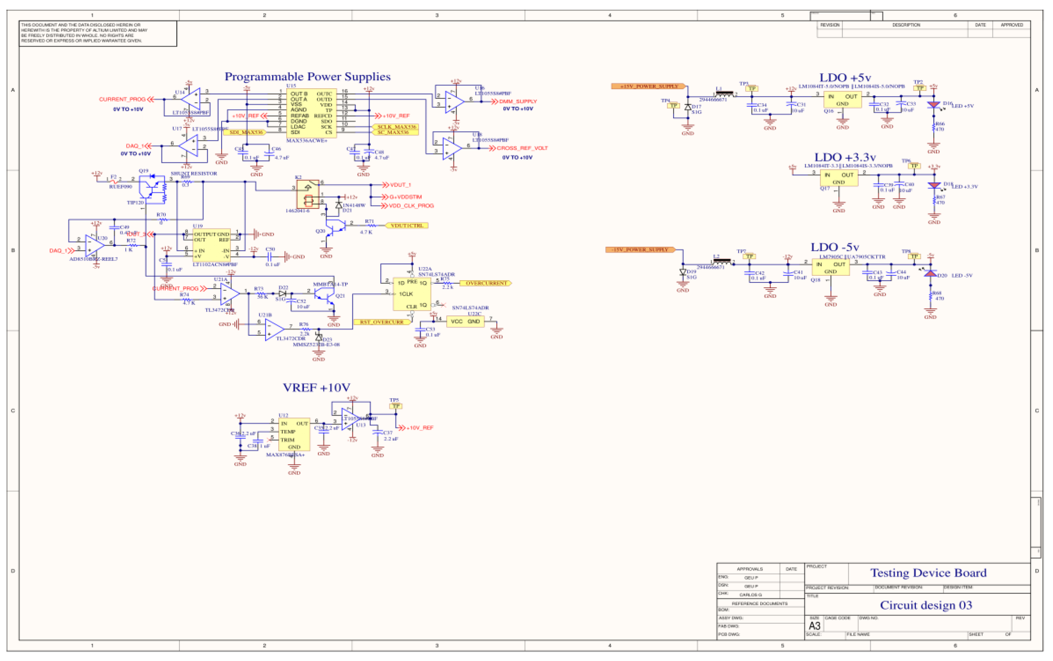
Figure A4.
Circuit design: General-purpose inputs/outputs.
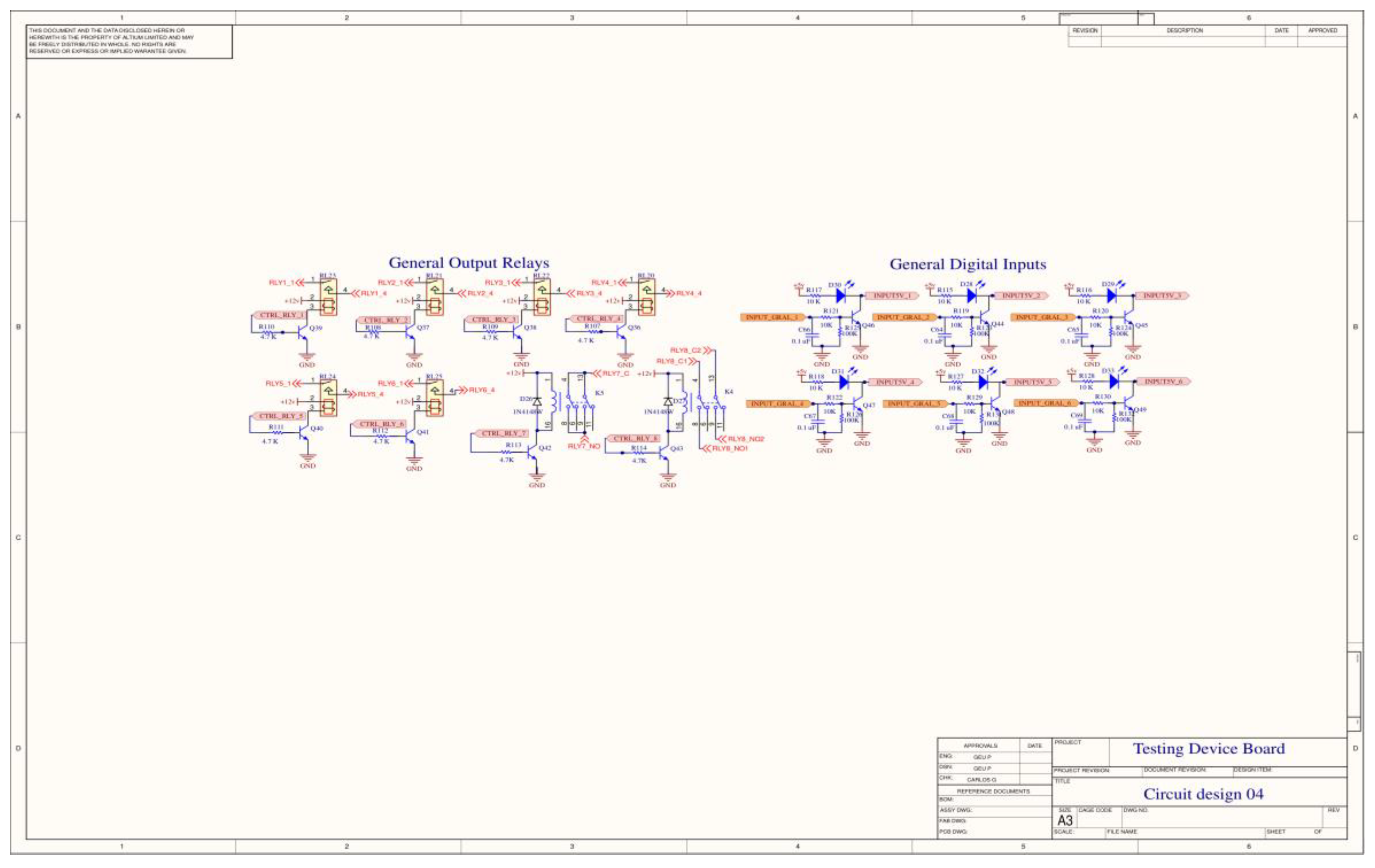
Figure A5.
Circuit design: signal amplification, audio conditioning, speed-up, and opto-isolated input design.
Figure A5.
Circuit design: signal amplification, audio conditioning, speed-up, and opto-isolated input design.
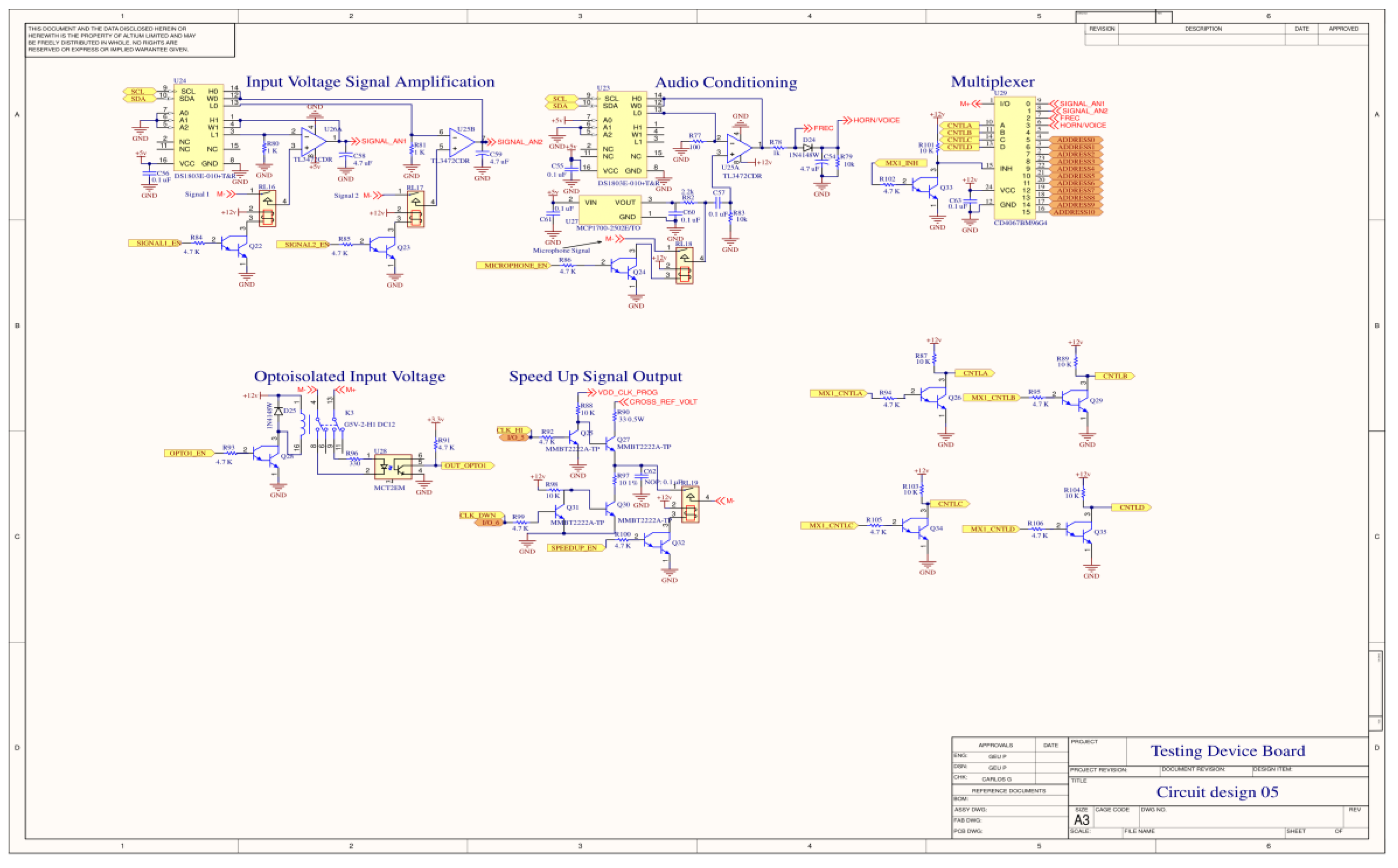
Figure A6.
Circuit design: Relay banks for M+, and M- buses.
Figure A7.
Circuit design: Relay banks for V+, and G- buses.
References
- Buckroyd, A. In-Circuit Testing; Butterworth-Heinemann: Oxford, UK, 2015. [Google Scholar]
- Gupta, R. Failure Mode and Effects Analysis of PCB for Quality Control Process. MAPAN 2023, 38, 547–556. [Google Scholar] [CrossRef]
- Hatzopoulos, A.A. Analog Circuit Testing. In Proceedings of the 2017 International Mixed Signals Testing Workshop (IM-STW), Thessaloniki, Greece, 3–5 July 2017; pp. 1–6. [Google Scholar] [CrossRef]
- Petkov, N.; Ivanova, M. Printed Circuit Board and Printed Circuit Board Assembly Methods for Testing and Visual Inspection: A Review. Bull. Electr. Eng. Inform. 2024, 13, 2566–2585. [Google Scholar] [CrossRef]
- Lai, J.-P.; Lin, Y.-L.; Lin, H.-C.; Shih, C.-Y.; Wang, Y.-P.; Pai, P.-F. RLC Circuit Forecast in Analog IC Packaging and Testing by Machine Learning Techniques. Micromachines 2022, 13, 1305. [Google Scholar] [CrossRef] [PubMed]
- Monagas Martín, J.E.; Nevado, A.S.; Martínez, A.V. Low Cost Programmable Modular System to Perform In-Circuit Test (ICT) Full Development of the Hardware, Software and Mechanics of an ICT Machine. In Proceedings of the 2016 Technologies Applied to Electronics Teaching (TAEE), Seville, Spain, 22–24 June 2016; pp. 1–7. [Google Scholar] [CrossRef]
- Oliveira, R.; Freitas, L.; Costa, D.; Vicente, J.; Gonçalves, A.M.; Malheiro, T.; Machado, J. A Systematic Analysis of Printed Circuit Boards Bending during In-Circuit Tests. Machines 2022, 10, 135. [Google Scholar] [CrossRef]
- Hough, D.G. The IEEE Standard 754: One for the History Books. Computer 2019, 52, 109–112. [Google Scholar] [CrossRef]
- Reverter, F. The art of directly interfacing sensors to microcontrollers. J. Low Power Electron. Appl. 2012, 2, 265–281. [Google Scholar] [CrossRef]
- Puentes-Conde, G.M.; Sifuentes, E.; Molina, J.; Enríquez-Aguilera, F.; Bravo, G.; Enríquez, G.N. Direct Interface Circuits for Resistive, Capacitive, and Inductive Sensors: A Review. Electronics 2025, 14, 2393. [Google Scholar] [CrossRef]
- Sherman, D. Measure Resistance and Capacitance Without an A/D: AN449; Philips Semiconductors Microcontroller Products; Philips Semiconductors: Eindhoven, The Netherlands, 1993. [Google Scholar]
- Webjör, Å. Simple A/D for MCUs Without Built-in A/D Converters: AN477; Motorola Semiconductors; MOTOROLA Ltd.: Chicago, IL, USA, 1993. [Google Scholar]
- Cox, D. Implementing Ohmmeter/Temperature Sensor: AN512; Microchip Technology: Chandler, AZ, USA, 1994. [Google Scholar]
- Richey, R. Resistance and Capacitance Meter Using a PIC16C622: AN611; Microchip Technology: Chandler, AZ, USA, 1997. [Google Scholar]
- Bierl, L. Precise Measurements with the MSP430; Texas Instruments: Dallas, TX, USA, 1996. [Google Scholar]
- Merritt, B. MSP430 Based Digital Thermometer; Application Report 1999; Texas Instruments: Dallas, TX, USA, 1999. [Google Scholar]
Figure 1.
Electrical Testing Mini-Position EOL device Board. (a) Top side, and (b) bottom side.
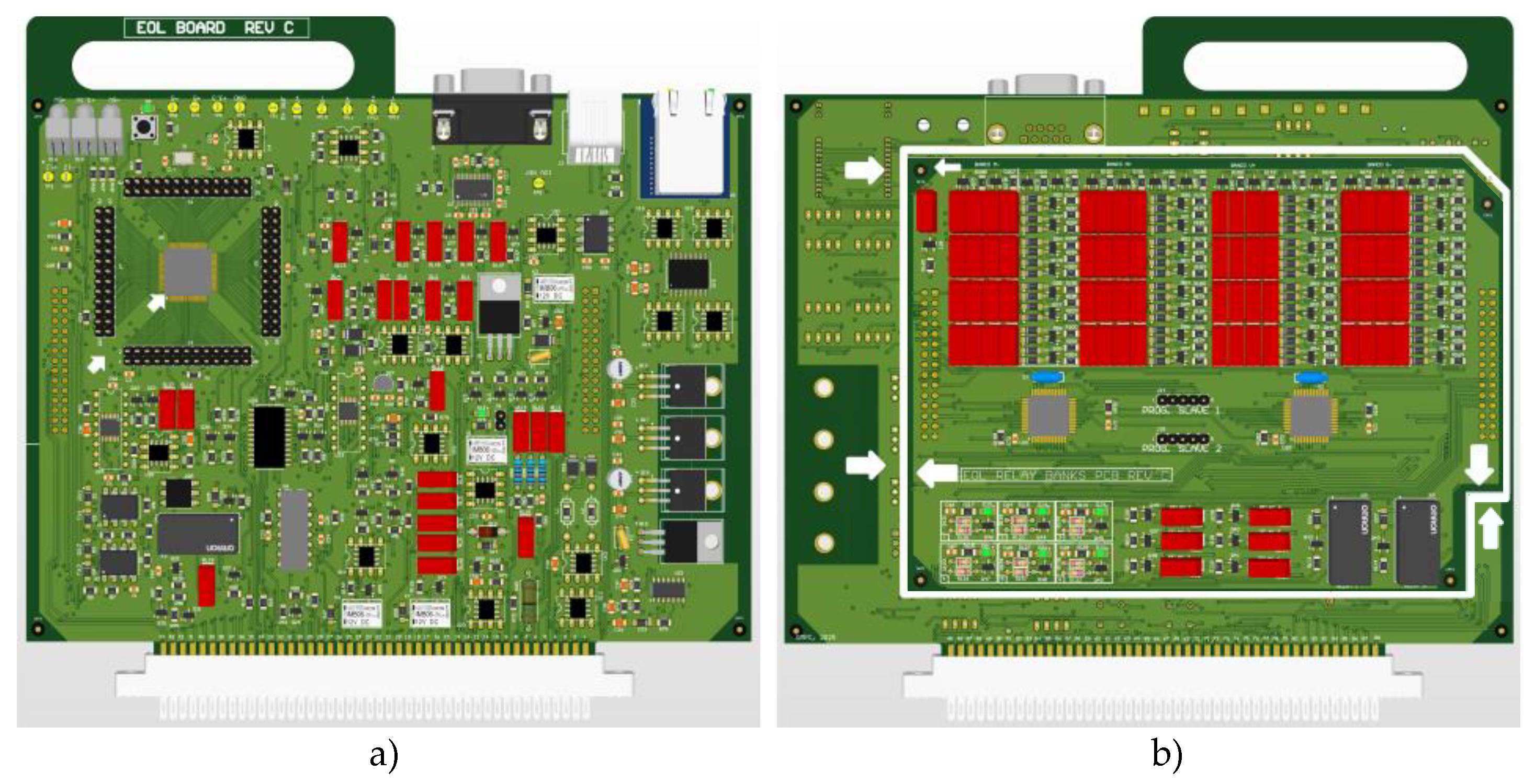
Figure 2.
An overview of the Electrical Testing Board architecture to perform testing tasks.
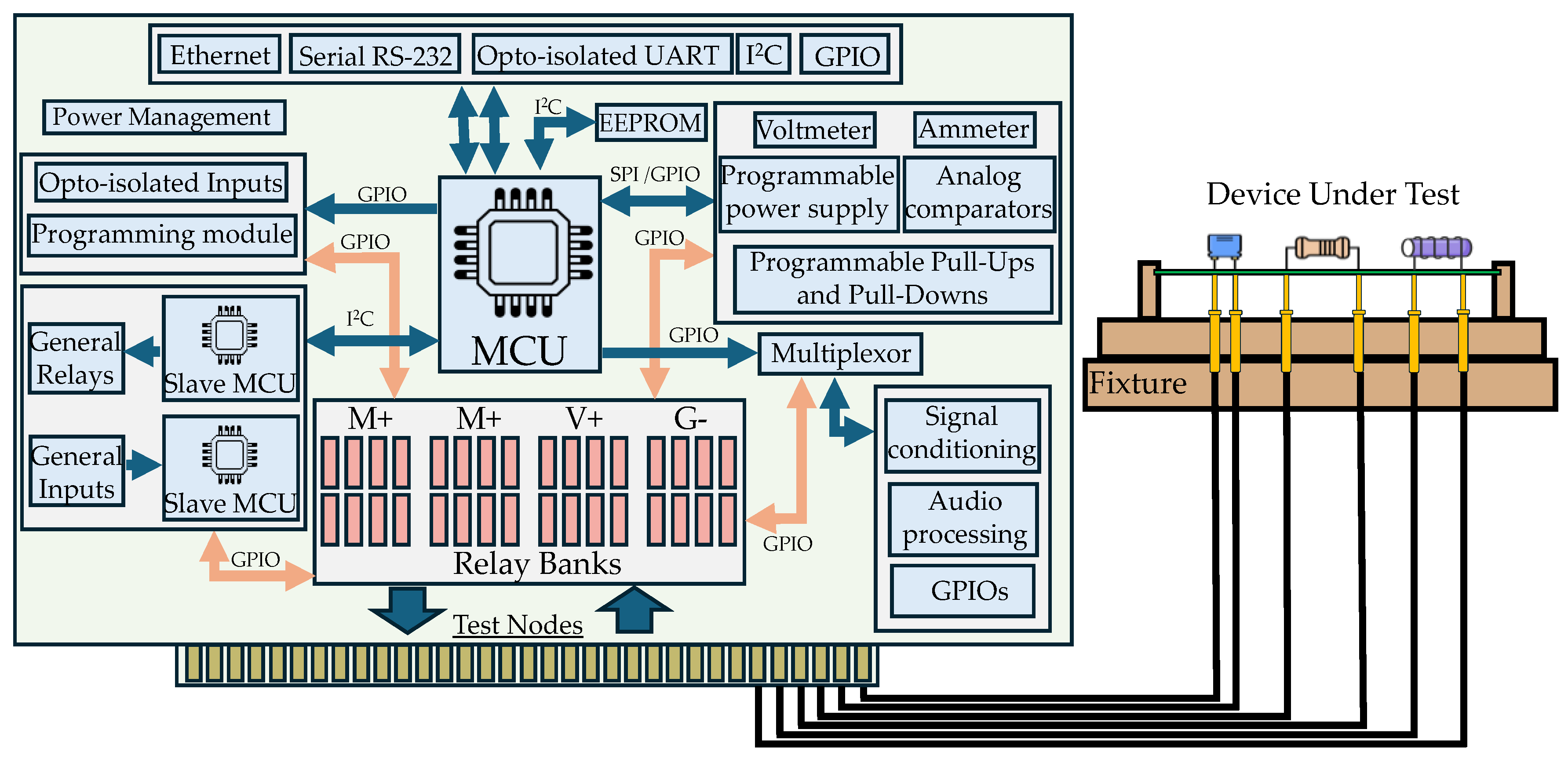
Figure 3.
Device board edge connector.
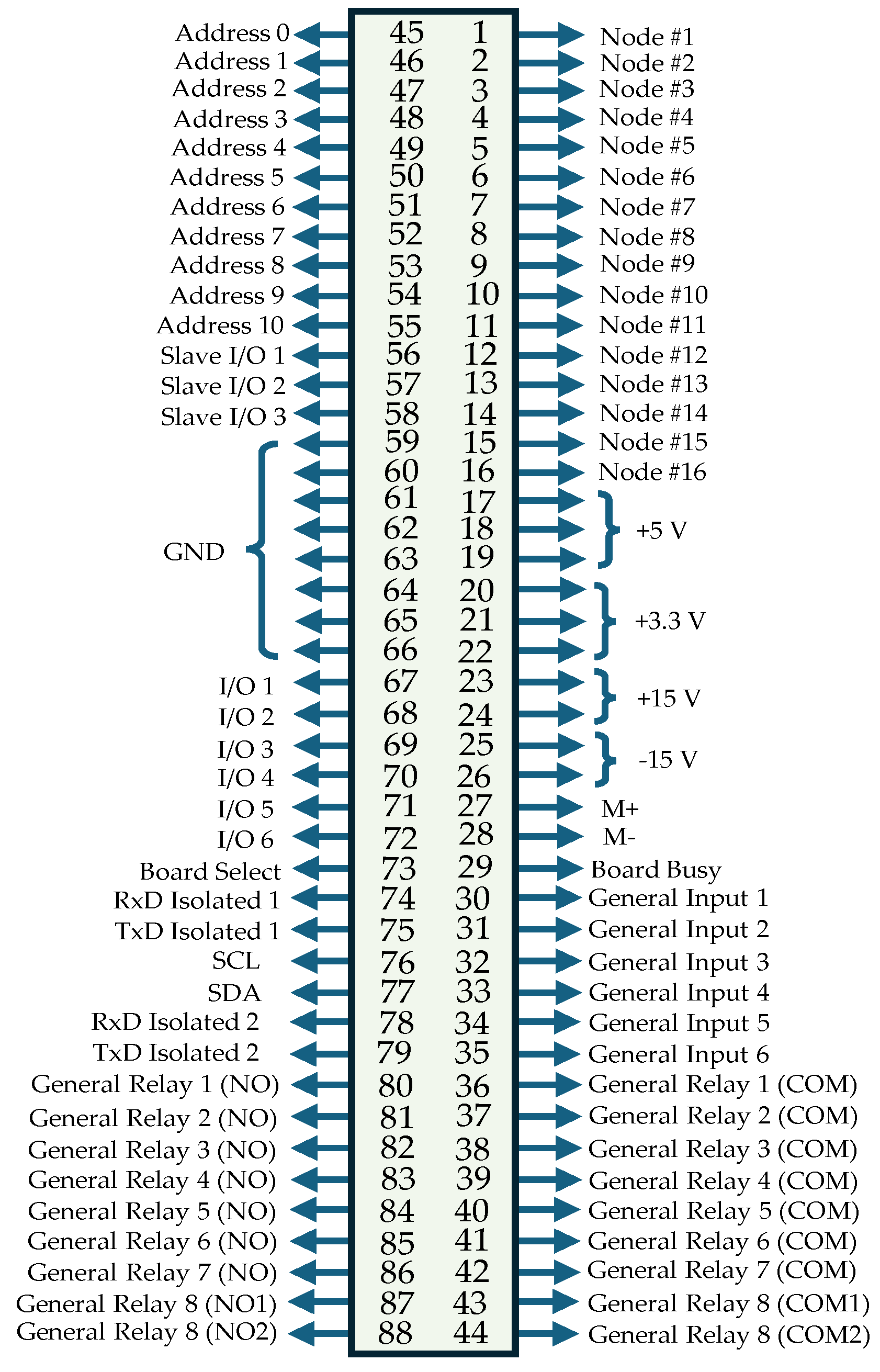
Figure 4.
Communication approach circuit: RS-232, Ethernet, and two opto-isolated UARTs.
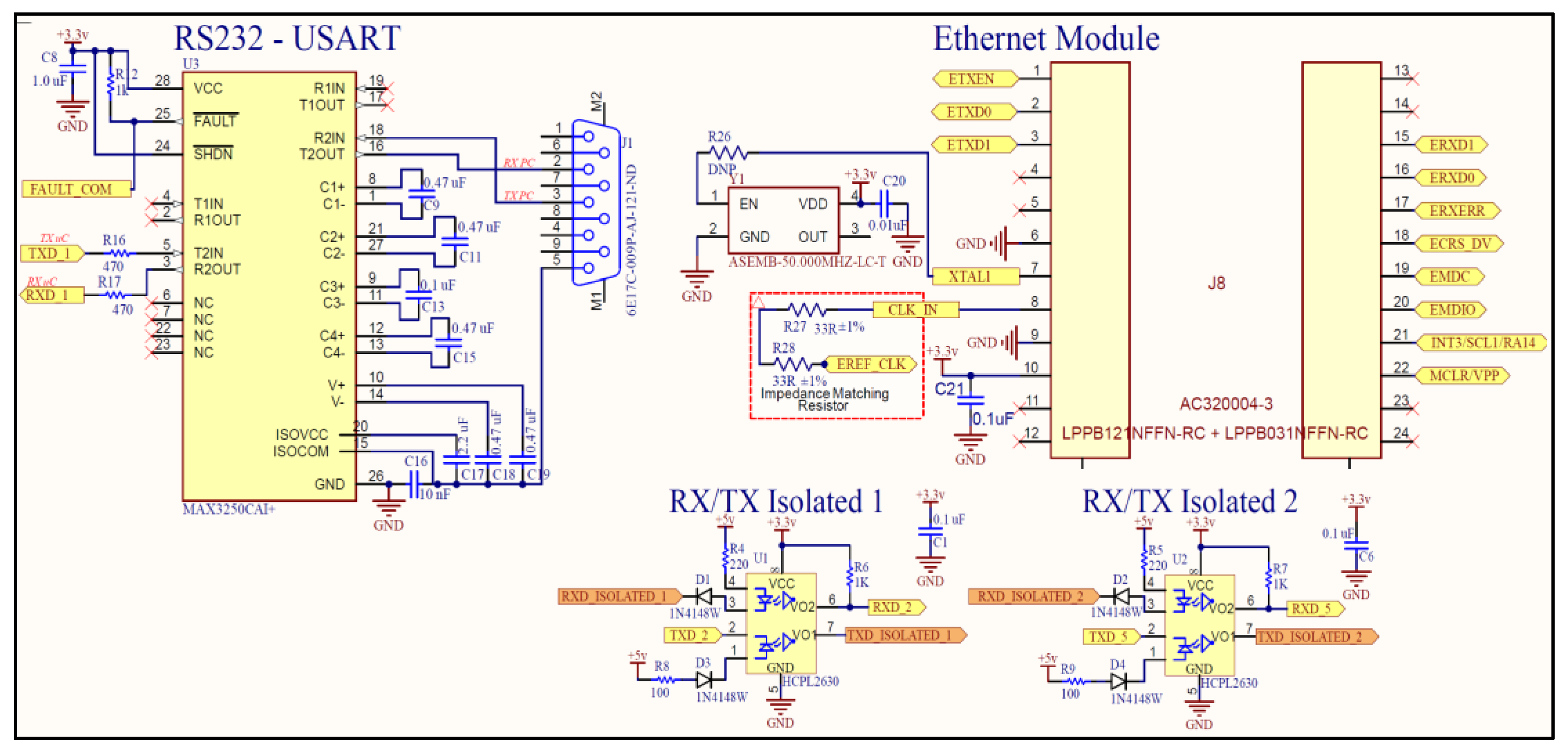
Figure 5.
Frame packet.

Figure 6.
Packet data example.
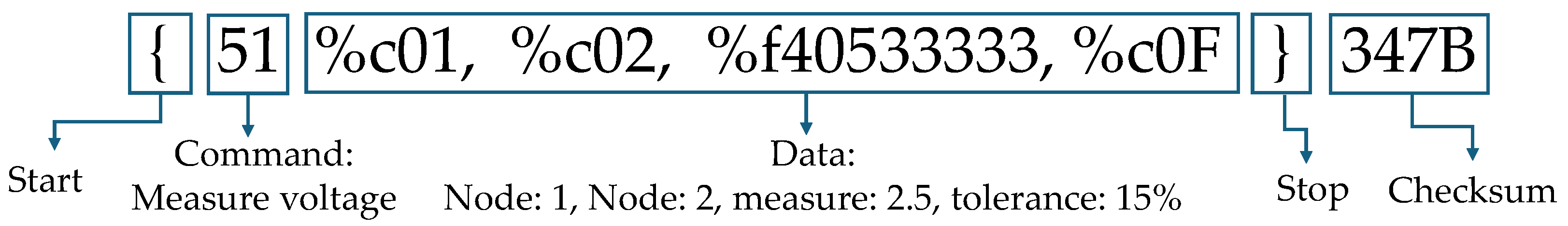
Figure 7.
G- Relay Bank representation with 16 test node circuits.
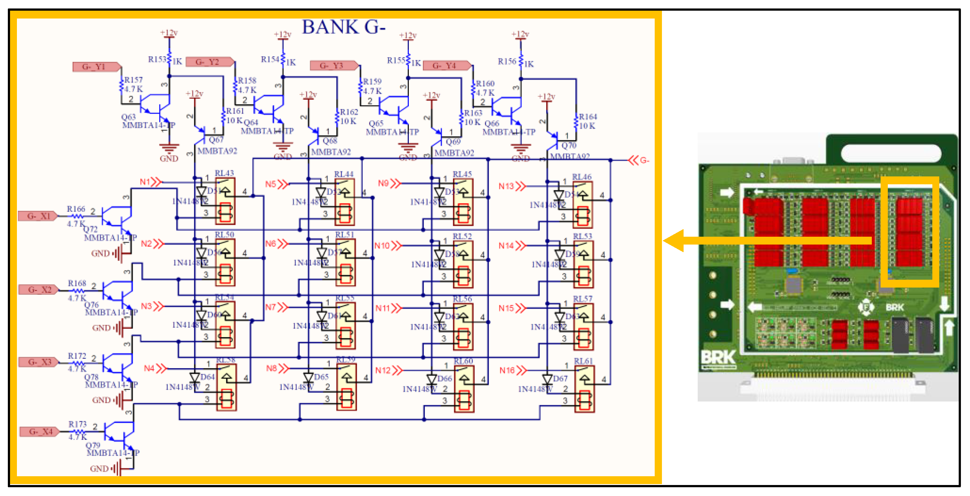
Figure 9.
V+ Relay Bank and optional discharging circuit.
Figure 10.
Analog comparators, pull-ups, and pull-downs to the M+ and M- buses circuit.
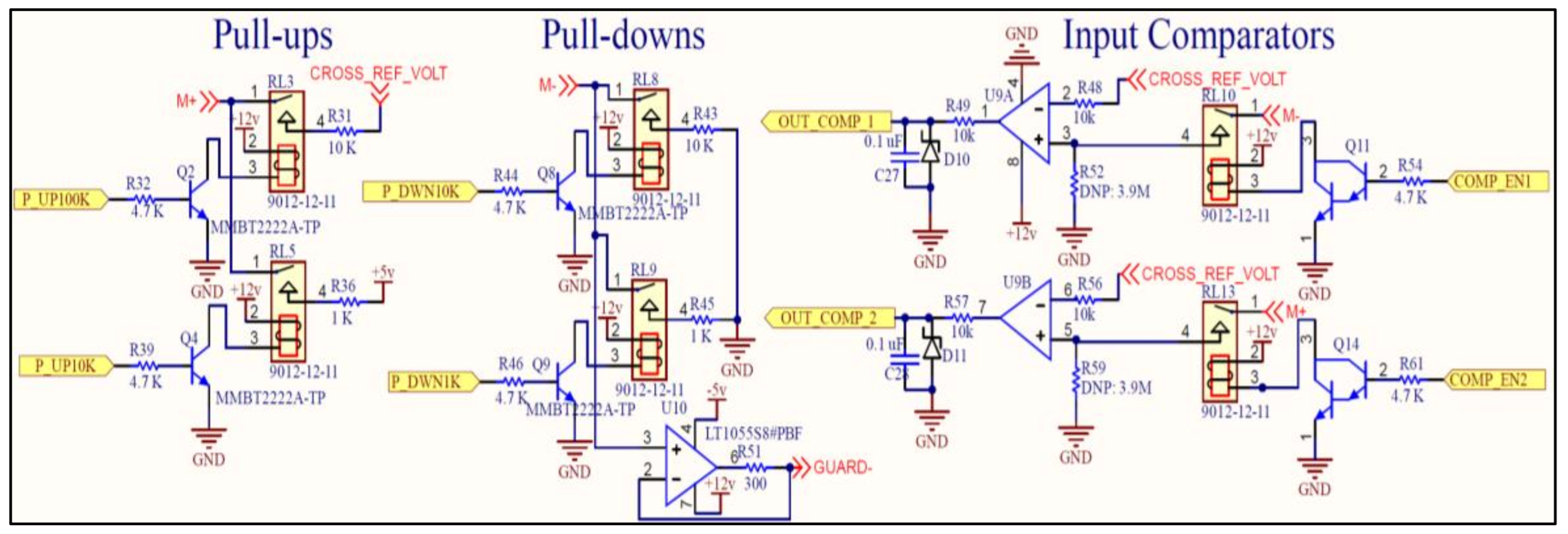
Figure 11.
DMM; voltmeter and ammeter circuit.
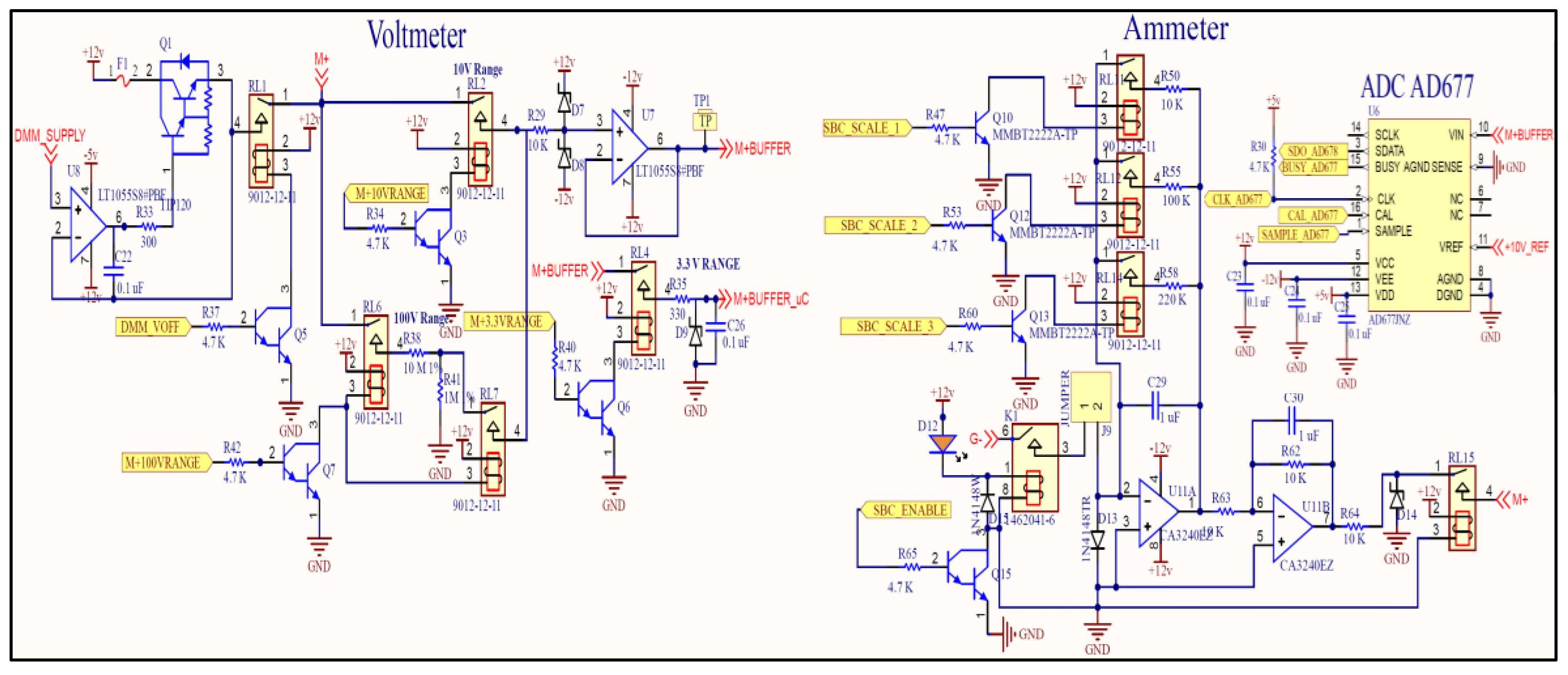
Figure 12.
Resistance measurement principle.
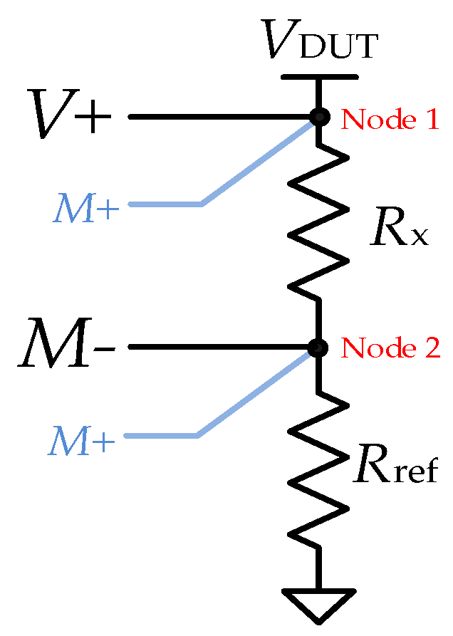
Figure 13.
Direct interface circuit for capacitance measurement [10].
Figure 13.
Direct interface circuit for capacitance measurement [10].
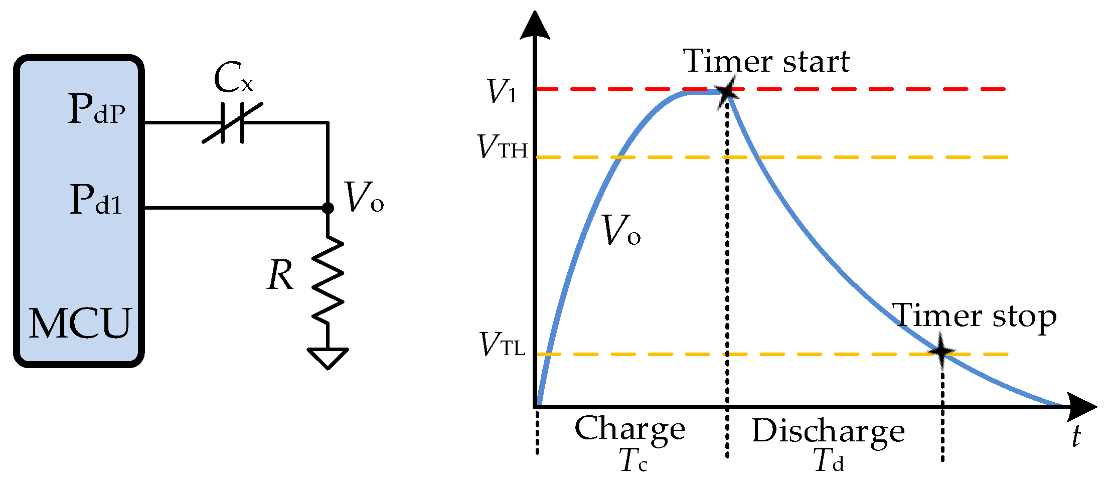
Figure 14.
Capacitance measurement principle.
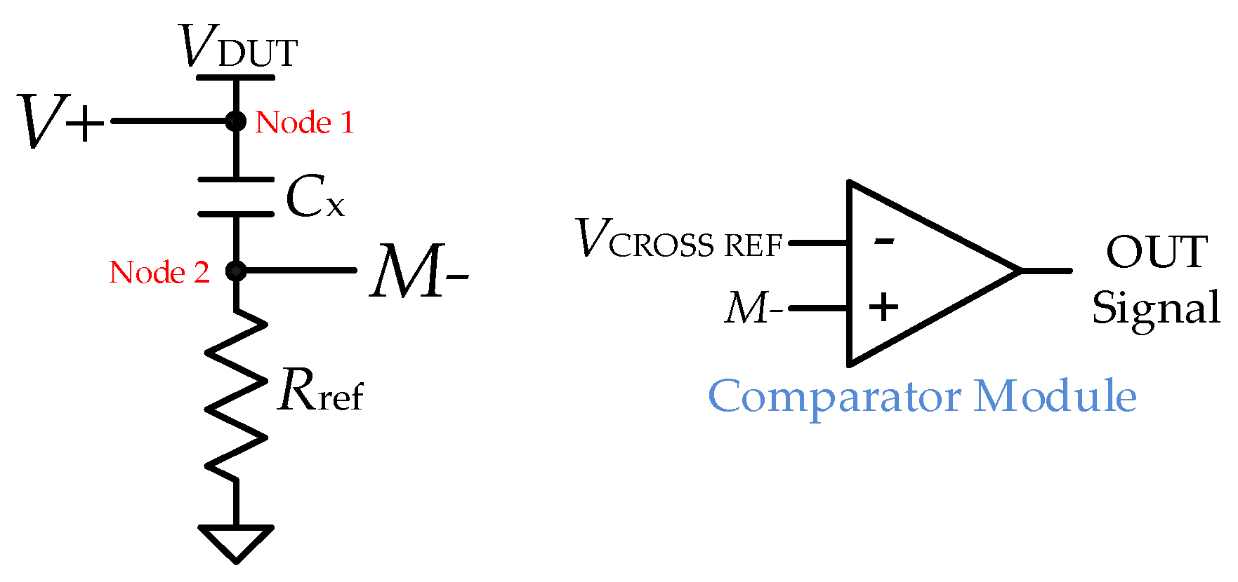
Figure 15.
Analog signal amplification, audio conditioning, and multiplexing circuits.
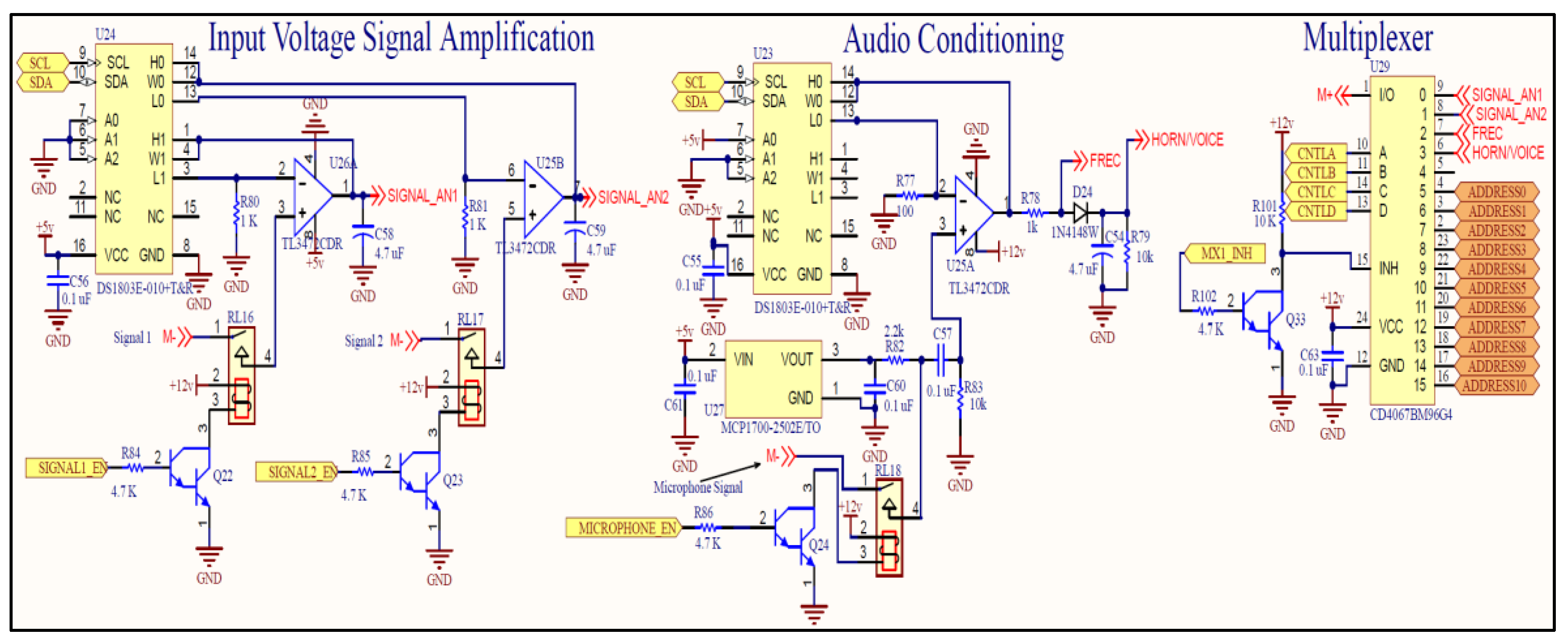
Figure 16.
An opto-isolated general input circuit, speed-up PWM signals, and an EEPROM circuit.
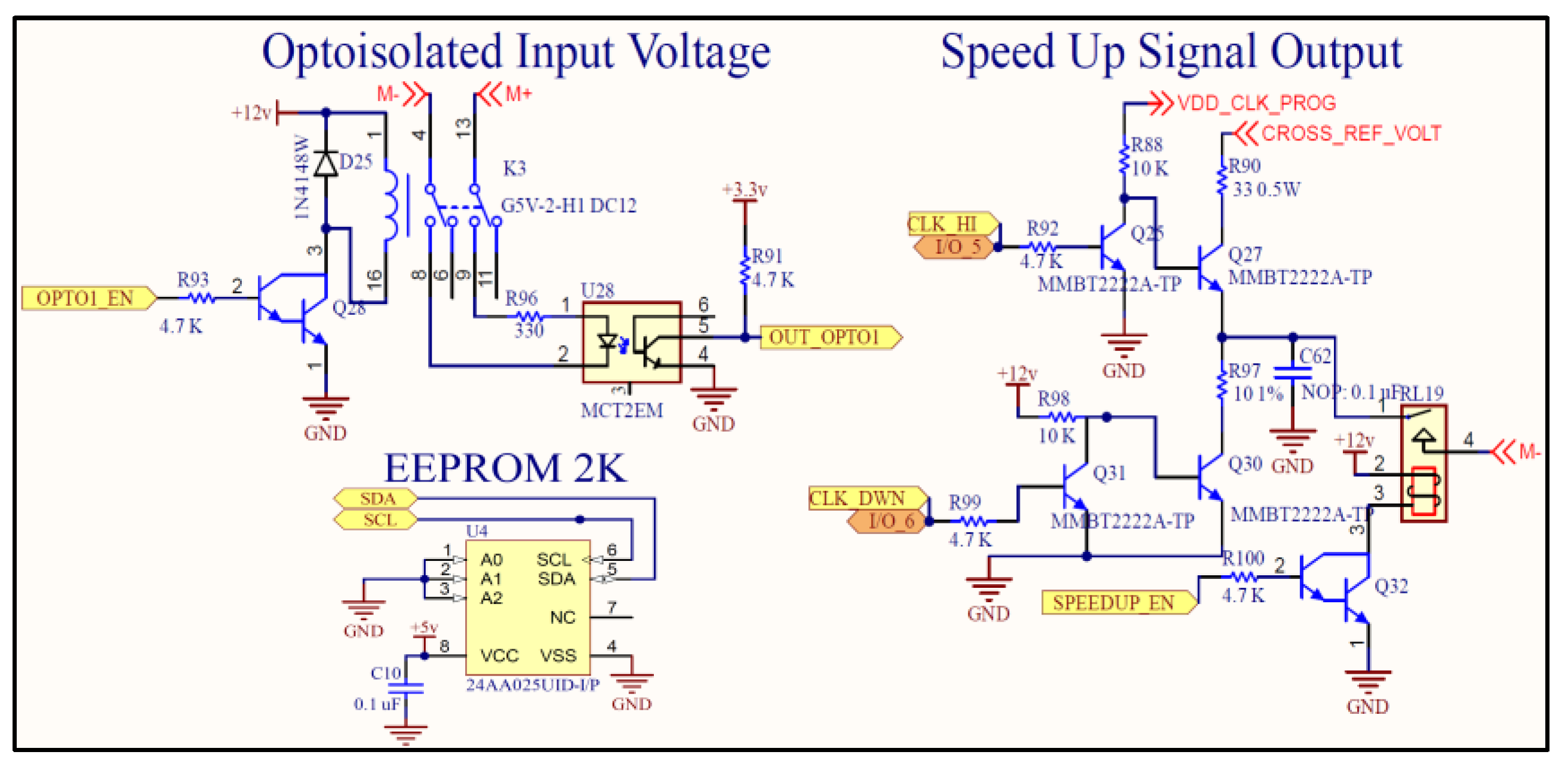
Figure 17.
General output relays and a general high-voltage digital inputs circuit.
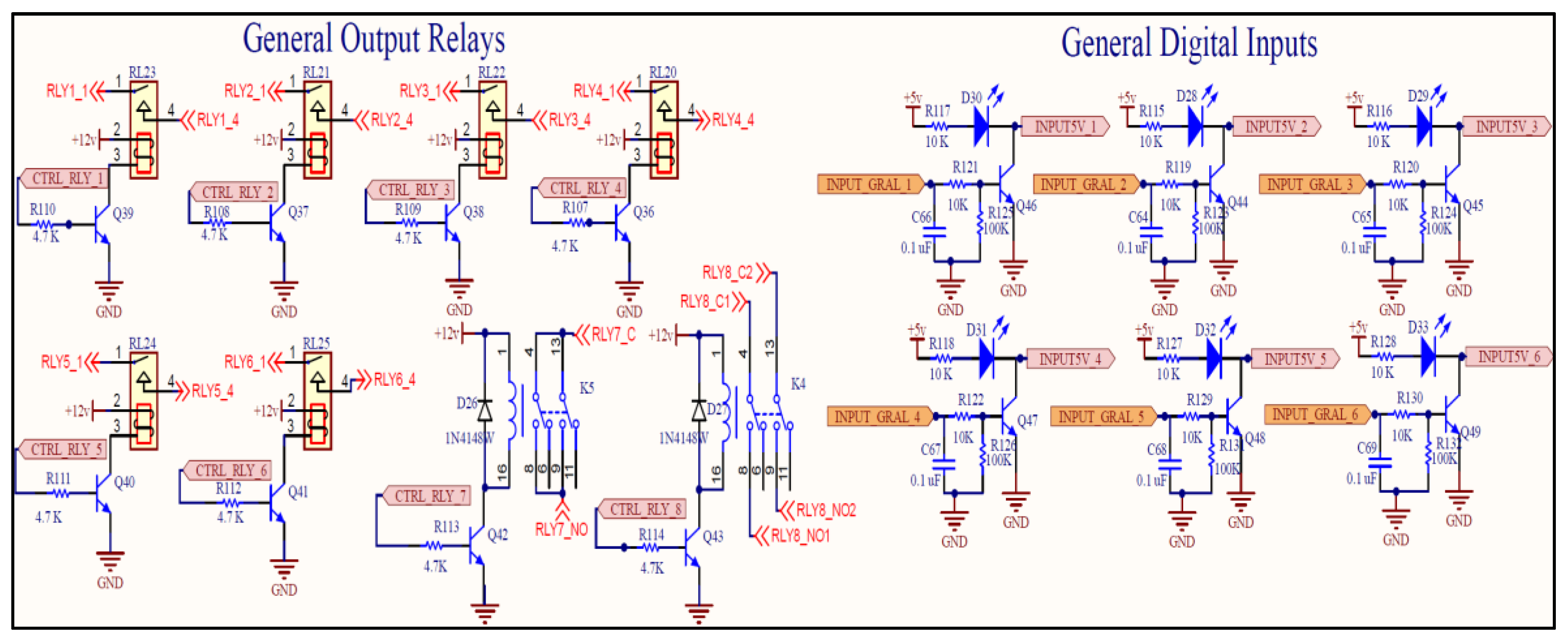
Figure 18.
Overview of the testing device board implementation.
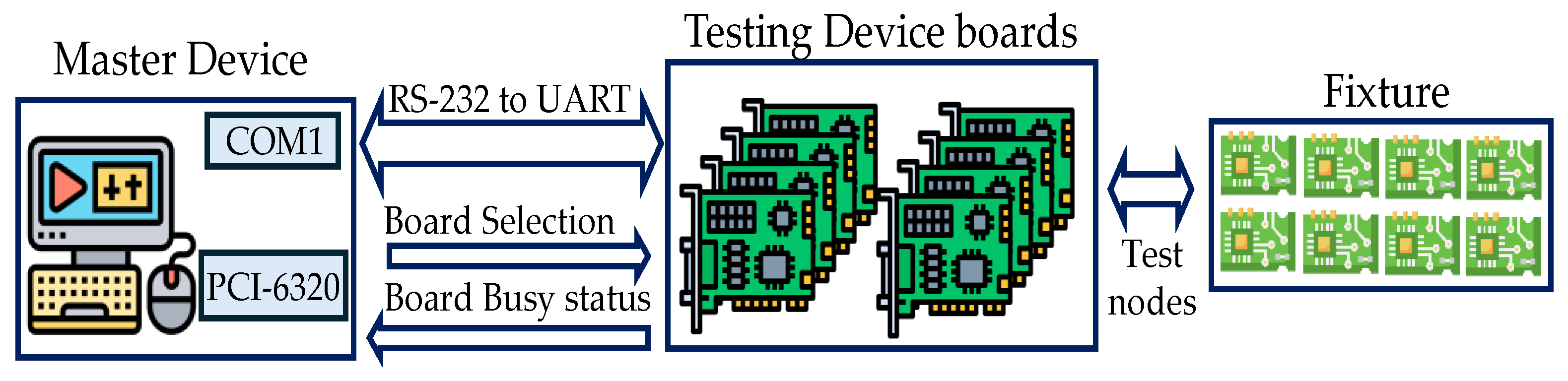
Figure 19.
Control process flow for a single testing device board.
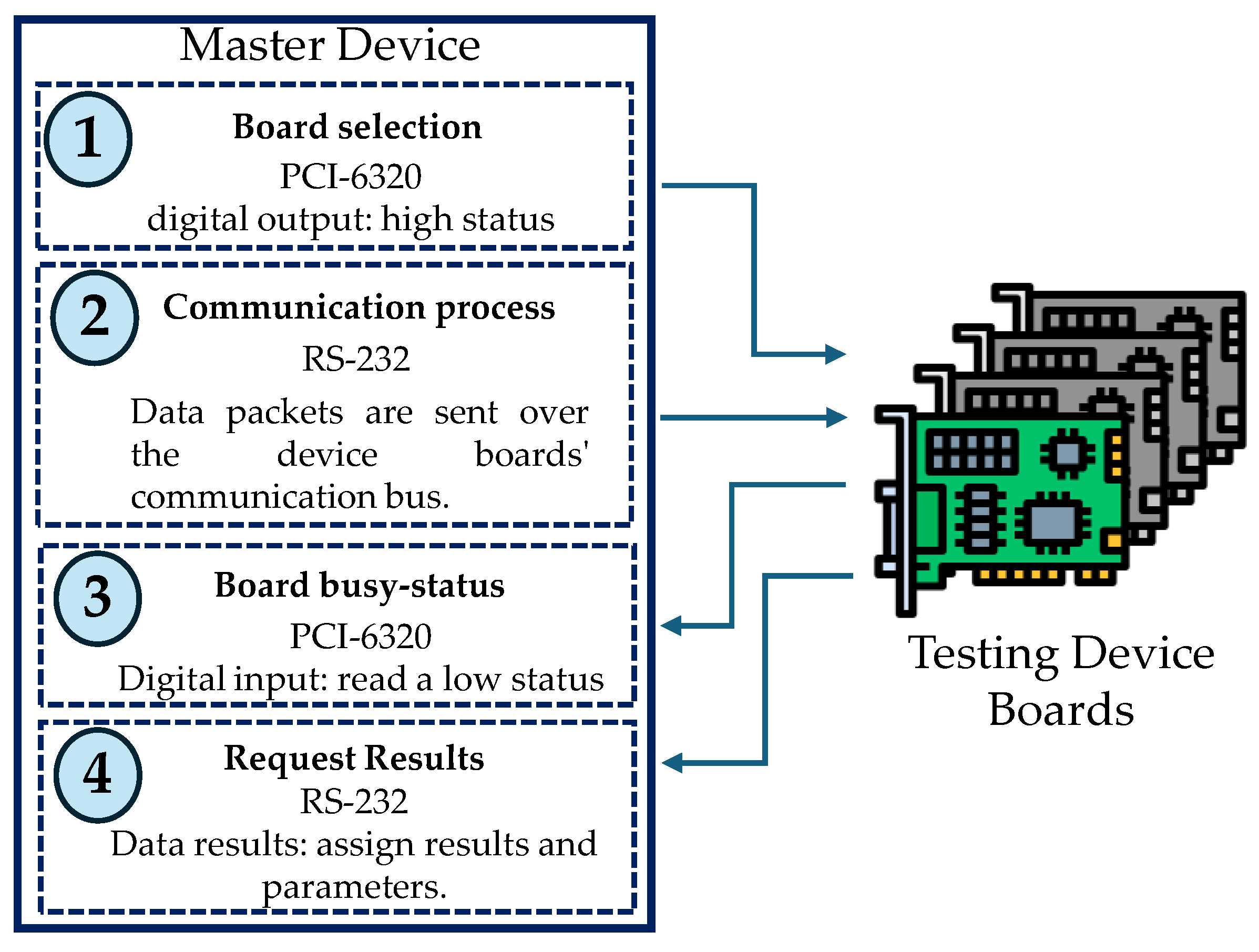
Figure 20.
Hardware device board.
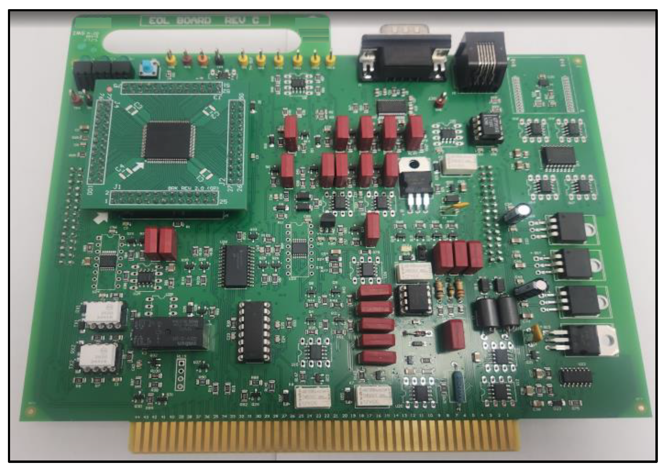
Figure 21.
(a) A graphical user interface, and (b) a device board hardware box.
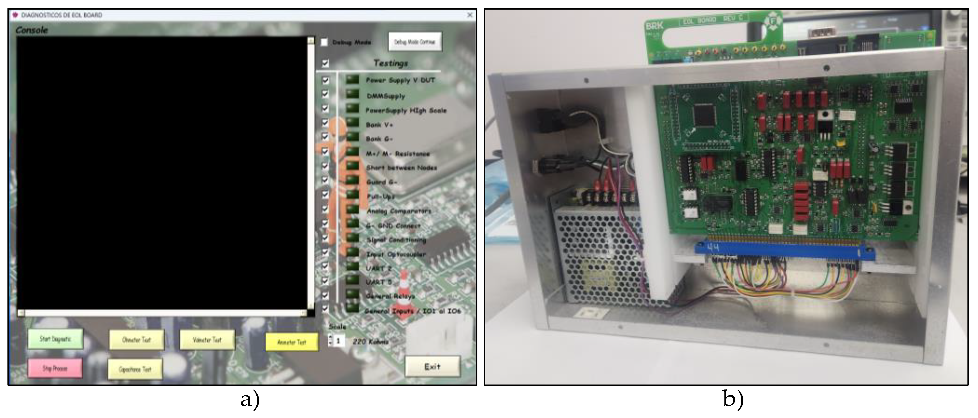
Figure 22.
Automated test equipment: (a) a fixture pallet with eight nests for each DUT, (b) pogo pins fixture nodes, and (c) testing device boards for each nest in the fixture pallet.
Figure 22.
Automated test equipment: (a) a fixture pallet with eight nests for each DUT, (b) pogo pins fixture nodes, and (c) testing device boards for each nest in the fixture pallet.
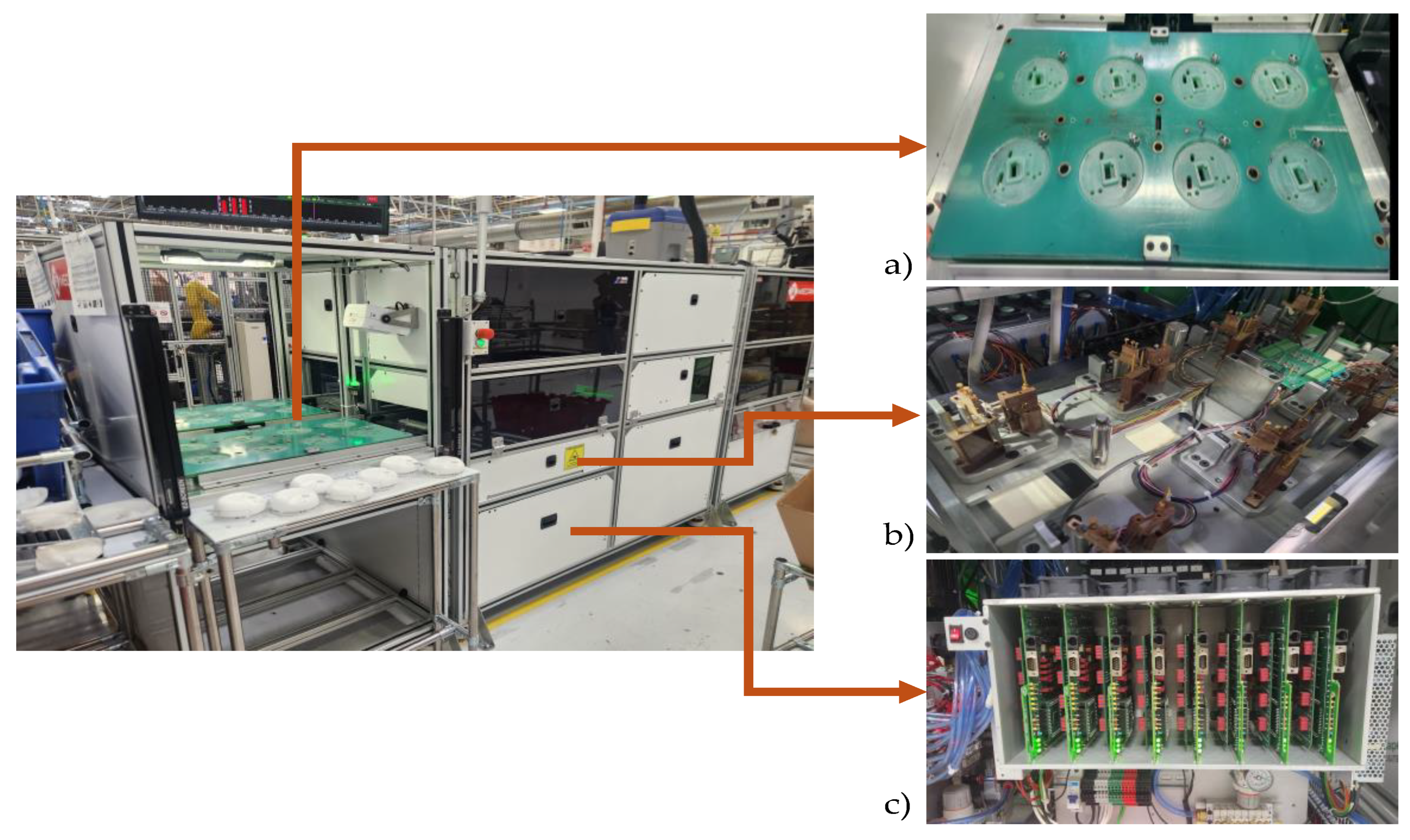

Table 1.
Data type formatting.
| Data type | Identifier | Value | Representation | ASCII Conversion |
|---|---|---|---|---|
| Char | %c | 91 | hex-format: 0 × 5B | ‘5’, ‘B’ |
| Integer | %i | 13,675 | hex-format: 0 × 356B | ‘3’, ‘5’, ‘6’, ‘B’ |
| Float | %f | 8.95 | float to IEEE754 32-bits: 0 × 410F3333 | ‘4’, ‘1’, ‘0’, ‘F’,’3, ‘3’, ‘3’, ‘3’ |
| String | %s | ‘b’ | no changes | ‘b’ |
Table 2.
MCU pin configuration and measurement procedure of a capacitive sensor [10].
Disclaimer/Publisher’s Note: The statements, opinions and data contained in all publications are solely those of the individual author(s) and contributor(s) and not of MDPI and/or the editor(s). MDPI and/or the editor(s) disclaim responsibility for any injury to people or property resulting from any ideas, methods, instructions or products referred to in the content. |
© 2025 by the authors. Licensee MDPI, Basel, Switzerland. This article is an open access article distributed under the terms and conditions of the Creative Commons Attribution (CC BY) license (http://creativecommons.org/licenses/by/4.0/).
Copyright: This open access article is published under a Creative Commons CC BY 4.0 license, which permit the free download, distribution, and reuse, provided that the author and preprint are cited in any reuse.


