Submitted:
11 December 2025
Posted:
12 December 2025
You are already at the latest version
Abstract
This paper proposes an analog retuning strategy that strengthens the functional longevity of photovoltaic (PV) systems operating within circular-economy environments. Although PV modules can be relocated from large generation sites to low-demand rural or remote settings, their electrical behavior offers no adjustable quantities capable of extending service duration. In many cases, even after formal disposal or decommissioning, these solar panels still retain a considerable portion of their energy-generation capability and can operate for many additional years before their output becomes negligible, making second-life deployment both technically viable and economically attractive. In contrast, the associated power-electronic converters contain modifiable gate-driver parameters that can be reconfigured to moderate transient phenomena and lessen device stress. The method introduced here adjusts the external gate resistance in conjunction with coordinated switching-frequency adaptation, reducing overshoot, ringing, and steep dv/dt slopes while preserving the original switching-loss budget. A unified analytical framework connects stress mitigation, ripple evolution, and projected lifetime enhancement, demonstrating that deliberate analog tuning can substantially increase the endurance of aged semiconductor hardware without compromising suitability for second-life PV applications. Experimental results validated the study, confirming the effectiveness of the proposed approach for long-term deployment.
Keywords:
gate driver
; photovoltaic solar
; recycling panels
; circular economy
1. Introduction
The evolution of the circular market for electronics began with early policy-driven recycling programs for waste electrical and electronic equipment (WEEE) in the 1990s and early 2000s, when e-waste was framed primarily as an environmental and public-health liability, and research focused on describing collection systems, treatment technologies, and basic infrastructure for safe disposal and material recovery [1]. As extended producer-responsibility schemes and WEEE-specific directives matured, especially in Europe, formal take-back networks consolidated and laid the foundation for a traded secondary market in recovered components and metals. Global assessments such as the Global E-waste Monitor 2020 quantified the rapidly growing volumes of discarded electronics and emphasized their latent value and circular-economy potential, shifting the discourse from waste management toward resource governance [2]. In parallel, economic analyses of WEEE streams demonstrated that recycling of key product categories (e.g., information-technology equipment, displays, and PV-related electronics) can generate multi-billion-euro revenues, positioning e-waste as a profitable “urban mine” rather than a cost center [3]. Subsequent work on urban mining showed that, under realistic industrial conditions, recovering copper and gold from e-waste can approach or even outperform the costs of primary mining, further reinforcing the business case for circular markets in electronics [4]. More recent systematic reviews frame these developments explicitly within circular-economy theory, mapping how business models, reverse logistics, and regulatory frameworks in the WEEE industry and global e-waste management are converging toward closed-loop value chains in which reuse, repair, remanufacturing, and high-efficiency recycling are embedded as core design and policy principles [5,13].
Building on the broader evolution of circular markets for electronic systems, the photovoltaic (PV) sector has developed its own distinct circular ecosystem centered on the reuse, refurbishment, and recycling of power-conditioning (PC) electronics. As PV module degradation rates became better quantified, typically ranging from 0.2–1.5% per year depending on climate, technology, and operational stressors [7]. It became clear that inverters and electronics, rather than the PV modules themselves, often dictate system lifetime and replacement cycles. Foundational reliability studies demonstrated that power-electronic components such as electrolytic capacitors, gate-driver stages, and switching devices exhibit failure rates that dominate overall PV downtime [8,9], motivating research into remanufacturing, predictive maintenance, and extended-lifetime design. Concurrently, life-cycle assessments and techno-economic analyses revealed that inverter can be reused in low-cost, rural, or off-grid PV applications [10,11]. Recent circular-economy frameworks specific to PV systems emphasize closed-loop recovery of electronics, showing that systematic collection, testing, and redeployment of refurbished inverters can reduce environmental burdens while supplying secondary markets where demand for cost-effective PV hardware is rapidly growing [12,13]. Together, these studies position PV systems as a central pillar of the emerging circular-economy model for solar energy infrastructure.
This focus on the core electronic components, particularly the inverters and power conditioners, is critical because they manage the entire flow of energy produced by the solar modules and deliver it to the grid or load. To fully appreciate the role and scope of these circularity efforts, it is necessary to first establish the context of where these essential electronics fit within the operational architecture of a solar array. Figure 1 illustrates the complete energy-conversion chain associated with photovoltaic (PV) generation. The top portion of the figure shows a conventional grid-connected solar installation: a PV array produces DC power, which is conditioned by a DC–DC stage and subsequently converted to grid-compatible AC through a DC–AC inverter. The conditioned AC is delivered to distribution lines, which is, in turn, normally connected to residential and commercial loads, up through a transformer for integration into high-voltage transmission networks.
The lower portion of the figure decomposes the inverter architecture and focuses on the power-electronic interface where the gate-driver is highlighted as a device that is needed in both conversion stages, i.e., DC–DC and DC–AC converters. The bottom-right part of this overview figure provides a schematic-level view of the gate-driver circuitry, which includes power MOSFET, an isolation pulse transformer, a diode, push-pull configurations, and the external gate resistor. The gate driver resistor () plays a central role in both the overall conversion efficiency and the lifespan of the power-electronic components in a photovoltaic installation. A lower gate resistance typically enhances efficiency by enabling faster switching transitions and reducing dynamic losses; however, these sharper transitions increase electrical stress on the semiconductor devices, thereby shortening their operational lifetime. Conversely, increasing the gate resistance mitigates stress and extends device longevity, but at the cost of higher switching losses and reduced system efficiency. As a result, efficiency and lifespan become inherently competing objectives during the normal operation of a PV energy-conversion system.
There is a rapidly expanding market for reused photovoltaic modules and second-life power-electronic hardware, driven both by the global push toward circular-economy practices and by end-users who can meaningfully benefit from the rural (or remote) energy production of aging PV systems. While these components often remain operational, their electrical characteristics drift significantly over time, leading to mismatches between the degraded PV source and the originally designed operating conditions of the associated power-electronic converters. In this context, simply reusing the inverter or gate driver circuitry with its factory-defined settings, particularly those calibrated to maximize efficiency in new, high-performance installations, can inadvertently punish lifespan and wear-out mechanisms in already aged devices. Consequently, retuning key parameters such as the gate-driver resistance becomes essential to restore a balanced trade-off between efficiency and reliability, ensuring that repurposed PV systems operate safely and predictably rather than failing prematurely due to conditions no longer aligned with their degraded state.
In this paper, an analog-based electronic approach is introduced to address a central challenge in realizing a genuinely sustainable circular economy for photovoltaic (PV) systems, i.e., the preservation of power-electronic component longevity when second-life PV modules and their associated converters are redeployed in new installations. As the secondary market for photovoltaic equipment grows increasing numbers of aged PV panels and power converters are being given a second life. However, the power-electronic converters that accompany these modules are frequently reused with their original factory calibration parameters. The proposed solution directly addresses this challenge through a cost-effective analog circuit implementation that adapts the converter’s operating conditions to the actual state of the reused hardware, thereby extending component lifetime while preserving overall system performance.
2. Solar System Circular Market - State-of-the-Art
Photovoltaic (PV) solar energy has become a central component of the global transition toward a low-carbon economy. National and international policies aimed at reducing emissions and improving power-grid resilience, combined with falling installation costs, have continuously driven the expansion of PV systems worldwide [14]. According to the 2025 report of the IEA PVPS programme, global cumulative installed PV capacity surpassed 2.2 TW by the end of 2024 [15]. This rapid growth, together with the increasing volume of decommissioned equipment, has raised economic, environmental, and supply-chain concerns, reinforcing the necessity of a circular-economy framework for PV technologies.
The circular-economy model for PV systems is generally structured around three pillars: (i) high-level strategies such as rethinking business models, reducing material consumption, and increasing modularity; (ii) life extension through reuse, repair, remanufacturing, and upgrading; and (iii) material recovery, including recycling and energy recovery [16].
Currently, the PV sector is dominated by a linear economic model, in which only a limited number of manufacturers design products for extended durability or recyclability [17]. Few companies repair or remarket used modules, and although the number of recyclers is growing, most recover only bulk materials, leaving behind valuable streams such as silver, copper, and high-purity silicon [18]. Strengthening circular practices can expand market opportunities, generate jobs, enhance supply-chain resilience, and reduce environmental impacts, thus motivating both governmental and private investments.
Figure 2 illustrates a circular-economy framework of products, emphasizing the flow of materials, components, and functional value throughout a product’s lifecycle. The cycle begins with resource extraction, represented by raw material acquisition from the environment, which feeds into product design and material selection. This stage determines the architecture, material composition, and long-term sustainability of the device. The flow then proceeds to manufacturing, where components are assembled into functional products.
After entering the use phase, products deliver their intended functionality until reaching the end of their primary service life. At this point, several circular-pathway options emerge. Reuse retains the product’s form and function with minimal intervention, allowing it to be reintroduced into service. Remanufacturing involves disassembly, replacement of worn elements, and reassembly to restore product-level functionality—depicted in the figure by the return loop from the user back to the manufacturing stage. Recycling recovers raw materials, which reenter the earlier design or manufacturing stages. Items that cannot be recovered follow a final path to disposal.
Module degradation rates typically range from 0.2% to 1% per year (other references mentioned 1.5%/year), with modules sometimes retaining roughly 85–90% of their rated capacity after two decades [19]. As a result, many retired modules remain suitable for secondary applications. Direct reuse may be feasible for modules removed early, whereas others may require repair before redeployment. Access to low-cost used equipment can accelerate PV adoption in underserved markets, including low-income and remote communities [17]. Moreover, resale or donation of early-decommissioned equipment can generate economic value for system owners, increasing total lifetime benefits through shared costs between primary and secondary users [18].
Recycling constitutes another important pillar of PV circularity. Mechanical, thermal, and chemical processes allow the recovery of high-value materials such as glass, silicon, indium, silver, tellurium, and copper [20]. Peripheral components—including junction boxes, wiring, and mounting structures—also contribute recoverable metals such as aluminum, steel, and copper. Efficient recycling not only mitigates environmental impacts but also reduces raw-material dependence, which is particularly relevant for silver and tellurium, whose supply chains face long-term constraints. Global projections estimate that recovered PV materials may exceed $15 billion by 2050 [20]. Reuse remains the most sustainable pathway, extending service life, diluting embodied energy, and delaying end-of-life processing. Functional but underperforming modules can be repurposed for secondary applications such as irrigation systems, off-grid lighting, or community-level social projects.
Landfilling is the least desirable option, as it discards valuable resources and introduces potential environmental risks. It should be considered only as a last resort and always in compliance with legal requirements.
Despite existing challenges, the repair–reuse–recycling triad increases the total lifetime value of PV systems and supports the emergence of new specialized services, such as reverse logistics, dismantling, and advanced recycling techniques. The expansion of circular-economy practices in the PV sector represents a critical step toward resource security, environmental protection, and long-term sustainability of the solar industry.
3. From Switch-Level Stress to System-Level Aging: Implications for PV Reuse
Figure 3 illustrates the fundamental influence of the external gate resistance on the MOSFET turn-on transient and, consequently, on the electrical stress imposed on the switching device. The figure presents two operating scenarios (low-stress and high-stress) each associated with a distinct choice of . The schematic at the top of the figure depicts a simplified “stress meter,” symbolically indicating how variations in gate resistance modulate overshoot, ringing, and levels.
The oscilloscope captures at the bottom of the figure provide empirical evidence of this behavior. In the left panel, corresponding to a larger gate resistance, the measured gate-source voltage exhibits a smooth, monotonic rise with minimal overshoot and negligible oscillatory behavior. This indicates a damped, low-stress switching event, in which the slower charge injection into the gate capacitances moderates the electric-field transients experienced by the MOSFET. Conversely, the right panel, associated with a smaller gate resistance, shows a substantially sharper transition in , accompanied by pronounced overshoot and ringing. These features are characteristic of high-stress switching, where the rapid and rates elevate the device’s susceptibility to wear-out mechanisms such as bond-wire fatigue, junction degradation, and parasitic-oscillation-induced overstress.
Across both panels, the microcontroller-level signal remains essentially unchanged, emphasizing that the differences in stress originate solely from the analog tuning of the gate resistance rather than from upstream digital control. Thus, Figure 3 visually reinforces the central principle motivating the proposed methodology: increasing reduces instantaneous switching stress at the expense of increased switching losses, whereas decreasing enhances efficiency but accelerates device aging. This trade-off becomes especially critical in circular-economy contexts where aged PV converters must be preserved and repurposed for extended operation under degraded electrical conditions.
While the gate-driver behavior defines the stress environment experienced by the power-electronic switch, the upstream PV source itself also evolves significantly as it ages. In reused systems, the converter must interact with a PV generator whose electrical characteristics no longer resemble those assumed in its original factory calibration. Consequently, understanding how degradation reshapes the power–voltage behavior of second-life PV modules is essential, because these altered source conditions directly influence operating points, current stresses, and the suitability of lifetime-extending strategies such as gate-resistance retuning. In this broader system-level perspective, device-level stress mitigation and PV-source degradation are tightly coupled aspects of the same circular-economy challenge.
The electrical characteristics of reused or degraded solar panels, specifically their Power versus Voltage (P-V) behavior, show marked differences from new modules, primarily due to internal degradation that reduces overall maximum power output. The most noticeable effect is the reduction in the Maximum Power Point (), causing the peak of the P-V curve to shift downward. This power loss is often driven by a decrease in the Short-Circuit Current (), which is sensitive to physical damage, soiling, and encapsulation discoloration that block sunlight from reaching the cells. Conversely, the Open-Circuit Voltage (), which defines the curve’s extent along the voltage axis, tends to be more stable and less affected by aging, though poor thermal management or severe Potential Induced Degradation (PID) can cause it to drop. A key diagnostic feature of degradation is the reduction in the Fill Factor (FF), visible as a more rounded “knee” on the I-V curve, which is symptomatic of increased internal resistance, often due to corrosion or faulty interconnects. Buyers of secondary market panels must be vigilant for severe defects indicated by a stepped or notched curve, which suggests current mismatch from partial shading or faulty bypass diodes, or an abnormally low , which can signal irreversible PID.
Figure 4 (top) illustrates the variation of photovoltaic (PV) degradation rates (DR) across four climate categories, i.e., Tropical (A), Dry (B), Temperate (C), and Continental (D) using the median and mean annual degradation rates as reference indicators [7]. The median shows the central, common degradation behavior, while the mean captures the influence of outliers and highlights the variability or risk of severe degradation in certain conditions. Together, the mean and median provide a fuller statistical picture. The thick gray line denotes the median DR, while the thin black line represents the mean, enabling a comparison between the central trend and the influence of high-degradation outliers. A clear decreasing pattern emerges as climates transition from Tropical to Continental, i.e., PV systems operating in tropical regions experience the highest degradation rates, followed by those in dry climates, whereas modules installed in temperate and continental climates show the lowest degradation levels. This behavior reflects the strong influence of environmental stressors such as temperature, humidity, and irradiance, which accelerate material deterioration in harsher climates. The larger gap between the mean and median DR in tropical and dry regions indicates the presence of more extreme degradation cases, particularly among technologies sensitive to heat and moisture, while the closer alignment of these metrics in temperate and continental climates suggests more uniform long-term performance. The bottom part of Figure 4 shows the effect of compound annual degradation on the relative power output of a photovoltaic (PV) system over a 30-year lifespan with .
Let denote the normalized power output of a photovoltaic (PV) module at year t, with corresponding to the initial nominal power. Assuming an annual degradation rate of from year to and a different annual degradation rate of from year to , the evolution of can be modeled in discrete time as
where is the initial power, and . In this formulation, the first term captures the compounded degradation during the initial 30-year period, while the factor accounts for the accelerated or relaxed degradation regime in the extended lifetime from year 30 to year 50. Equation (1) ensures continuity at and provides a simple yet flexible framework for evaluating long-term performance and lifetime energy yield under distinct degradation regimes.
Figure 5 extends the two-phase degradation model presented earlier by illustrating not only the long-term decline of photovoltaic (PV) module output but also the opportunity for post-lifetime electronic adaptation. The solid black curve represents the initial 30-year operating period, during which the PV module undergoes a uniform degradation rate of 1.5%/year, leading to a normalized output of approximately 0.63 at year 30. Beyond this point, four distinct trajectories are shown, corresponding to different post-30-year degradation regimes (1%, 3%, 9%, and 20%/year). Larger DR values are not necessarily the case but they were included here for comparison purposes. The inset highlights an analog gate-driver circuit whose effective gate resistance can be manually or electronically tuned. This tuning mechanism becomes particularly relevant after the PV module’s nominal in-service lifetime has been reached (in this case 30 years).
Although PV modules can be relocated from a primary installation, such as a utility-scale generation plant, to secondary sites with lower power demand in rural or remote regions, their intrinsic electrical characteristics offer no tunable parameters capable of extending their in-service lifespan. By contrast, the accompanying power-electronic converters possess adjustable operating conditions, particularly within the gate-driver stage, that can be deliberately retuned to mitigate switching stress and thereby expand the equipment’s effective service lifetime. Thus, Figure 5 not only visualizes the projected degradation profiles but also emphasizes the role of adaptive analog electronics in preserving system robustness as the PV generator ages.
4. Analog Electronics Intervention: Stress Mitigation Without Sacrificing Efficiency
4.1. New Operating Frequency Defined by Retuning
Figure 6 illustrates the conceptual impact of gate-resistance retuning on the switching behavior of a power semiconductor device, emphasizing how adjustments to both the gate resistance and the effective switching interval reshape the voltage–current trajectories and, consequently, the switching-loss profile. The top waveforms represent the original operating condition, where and are tuned to optimize efficiency for a newly manufactured product, also known as virgin product. The middle waveforms show the effect of modifying the gate resistance () while maintaining the same switching period (), which will lead to less switching stress in each transient but higher switching losses. To compensate that increase in losses, the proposed retuning strategy will change the switching frequency such that there is less switching events, as observed in Figure 6 (bottom).
Let the areas and represent the energy dissipated during switching transitions for the original and the new gate resistances, respectively.
For the original operating condition, the per-event energy and switching period are
Thus, the average switching power loss is
After retuning the gate resistance and changing the switching frequency, the new per-event energy and switching period become
leading to the new average switching loss
To maintain the same switching-loss budget after retuning the gate resistance, it is imposed
Even though the proposed retuning strategy results in a lower switching frequency, an intentional consequence of maintaining the original switching loss budget after increasing the gate resistance, the practical impact of this reduction is not considered detrimental for the intended application domain. As emphasized in this paper, most second-life PV converters can be redeployed in rural, remote, or fully off-grid environments, where operational constraints and performance expectations are significantly less stringent than in utility-scale or grid-tied installations. In these contexts, modest reductions in switching frequency do not compromise power quality or energy-conversion capability in any meaningful way, especially when contrasted with the substantial gains in component lifetime and stress mitigation obtained through analog retuning.
4.2. Consequence on Ripple (DC Converters): The Trade-Off for Extended Life
The reduction in switching frequency derived previouly also affects secondary dynamic quantities of the DC-DC boost converter, particularly the inductor-current ripple and the output-voltage ripple. For a boost converter operating in continuous conduction mode (CCM), the peak-to-peak inductor-current ripple satisfies
Using the retuning condition established in (11), the normalized ripple expressions become
Evaluating these relationships for the representative retuning factors , , and yields practical insight into the magnitude of the ripple variations. For , the switching-frequency reduction is only , producing a negligible increase in inductor-current ripple and a modest rise in output-voltage ripple. For , the inductor-current ripple increases by approximately , while the output-voltage ripple rises by about . Even with the deeper frequency reduction at , the inductor-current ripple increases by and the output-voltage ripple by .
5. Life-Time Modeling: From Gate Resistance to Device Longevity
The choice of impacts the calendar lifetime of the power switch, combining (i) a stress–versus–cycles-to-failure relationship and (ii) the effect of switching frequency on the accumulation of stress cycles over time.
From the gate-driver perspective, the MOSFET gate and source dynamics during switching can be approximated by an effective – network, where lumps the gate-source capacitance. In a first-order approximation, the dominant edge rate is given by
where is a constant for a given operating point. Faster edges (smaller ) are known to increase electric-field stress, overshoot, and oscillation amplitude, thereby accelerating wear-out mechanisms such as bond-wire fatigue and junction degradation.
To capture this effect analytically, a dimensionless electrical stress index is defined as
where is a reference gate resistance (e.g., the original factory setting) and is the corresponding nominal stress level. Equation (17) reflects the inverse relationship between and edge-related stress suggested by the transient waveforms in Figure 2, i.e., smaller values produce larger overshoot and ringing, whereas larger values yield more damped.
Power-semiconductor lifetime under repetitive switching can be approximated by an inverse power-law relationship between the cycles-to-failure and the applied stress index S:
where is the number of cycles to failure under the reference stress , and is a technology-dependent exponent obtained from power-cycling or accelerated life tests.
Substituting (17) into (18) yields a compact expression linking the cycles-to-failure directly to the gate resistance:
Equation (19) shows that, for , increasing the gate resistance () increases the allowable number of switching cycles before failure, because each event is less stressful from an electrical point of view.
The calendar lifetime can be written as
For the original, factory-calibrated operating condition,
After retuning the gate resistance to and applying the frequency scaling, the new lifetime is
Dividing (22) by (21) gives the normalized lifetime gain:
Equation (23) formalizes two concurrent effects: (1) the factor reflects the reduction in the number of switching events per unit time caused by lowering the switching frequency. Even if the stress per event were unchanged, this reduction alone would increase the calendar lifetime; (2) the factor captures the reduced electrical stress per switching transition due to a larger gate resistance, as indicated by the more damped waveforms and smaller overshoot observed for higher values.
Thus, for typical retuning scenarios with and , both mechanisms act in the same direction, leading to
i.e., an extended device lifetime relative to the original, efficiency-optimized factory setting.
In the context of reused or second-life PV converters, this is particularly valuable: the analog retuning of allows the same hardware platform to be operated in a lifetime-optimized regime, better aligned with the degraded PV source and the relaxed performance expectations of rural, remote, or off-grid applications, where lifetime extension and robustness often outweigh marginal gains in conversion efficiency.
The heatmap shown in Figure 7 was generated by evaluating the normalized lifetime–gain expression as a joint function of the switching–frequency ratio and the expected number of cycles experienced by the device. The lifetime–gain can be written as
To relate the analytical lifetime–exponent to a more physical degradation variable, the model adopts the widely used observation from power–cycling physics that the slope of the lifetime curve increases approximately with the logarithm of the number of cycles to failure. Thus,
which preserves consistency with the classical Coffin–Manson–type relations for fatigue accumulation in power semiconductors. Substituting (26) into (25) yields a two–dimensional gain function,
which was evaluated over the ranges and with fixed at , representing a moderate increase in gate resistance consistent with the retuning strategy proposed in this work. The resulting values of were then rendered as a heatmap with logarithmic scaling on the axis to reflect realistic field conditions of temperature and power cycling.
Figure 7 illustrates the predicted lifetime–gain surface as a function of the switching–frequency ratio (horizontal axis) and the total number of cycles (vertical axis, logarithmic scale). Warmer colors indicate higher lifetime gain. The plot reveals two fundamental behaviors: (i) reducing the switching frequency (lower ) systematically increases device lifetime, and (ii) devices operating under high cycle counts (large ) exhibit significantly larger sensitivity to gate–resistance retuning, reflecting the acceleration of wear–out mechanisms captured in (26). In combination, these behaviors demonstrate that even moderate increases in , implemented to reduce switching stress, may yield considerable lifetime improvements in long–duration photovoltaic applications, particularly where devices experience high cumulative cycling due to daily irradiance variations.
6. Experimental Results
To experimentally validate the proposed gate-resistance retuning strategy and its impact on switching stress, a hardware prototype was constructed using the isolated gate-driver topology employed throughout the analytical development. The objective of this setup is to reproduce the switching conditions relevant to reused or second-life PV converters and to directly measure how different values of external gate resistance modify the transient behavior of the MOSFET. The following describes the experimental gate-driver implementation used to obtain the waveforms and switching-energy measurements.
The circuit shown in Figure 8(a) implements an isolated push–pull gate driver for a high-voltage MOSFET. The microcontroller outputs a 0– logic signal. The signal drives two complementary BJT pairs (Q1–Q4) configured as a push–pull stage operating from a upper rail and a lower rail. These transistors generate a 12V ON and -12V OFF, which alternately energize the primary of the Murata 79604/9C transformer. The transformer provides a turns ratio for isolated gate drive. The capacitors and decouple DC from the drive path, ensuring that only the AC portion of the excitation is delivered to the MOSFET gate. The series resistor protects the push–pull stage in the event of transformer saturation by limiting the primary current. Figure 8(b) shows the photograph of the implemented re-tuned driver board, showing the power rail connector, push–pull stage, AC-coupling network (, ), transformer, and gate-interface components (, , , ) corresponding to the schematic in Figure 8(a).
On the transformer secondary, the resistor , in conjunction with the diode, provides a defined discharge and return path that removes the residual offset produced by AC coupling and ensures the gate reliably resets after each switching event. The gate resistor controls the MOSFET gate charge and discharge rates, shaping the switching transitions and regulating turn-on and turn-off behavior. The power stage applies to the MOSFET drain, and the device drives a purely resistive load. Table 1 displays component values used in the test circuit.
The three oscilloscope waveforms shown in Figure 9 demonstrate how the value of gate resistance governs the rate of the MOSFET’s switching transition and, consequently, the magnitude of switching stress on the device. When the gate resistance is set to , the switching waveforms exhibit the slowest and most gradual transitions among the three cases. The trace rises with a gentle slope, and both the and waveforms respond with smooth, extended transitions that contain virtually no observable ringing. The current waveform shows only minimal disturbance after the switching event, indicating that the high gate resistance effectively damps the influence of parasitic inductances and prevents excitation of oscillatory modes. This behavior reflects a very soft switching condition in which electrical stress on the device is minimized.
At a gate resistance of , the switching transitions become faster and more pronounced compared to the case, but still remain controlled and relatively smooth. The waveform rises at a moderate rate, and the corresponding changes in and occur over a shorter interval. Some small oscillations appear in the current waveform immediately following the transition. The voltage waveform settles more quickly than with , showing a moderate level of parasitic excitation. This intermediate gate resistance produces a balance between switching response and switching stress .
When the gate resistance is reduced to , the switching behavior becomes rapid and fast. The voltage rises very quickly, driving the MOSFET through its transition in a short interval and causing both and to change abruptly. These steep transitions lead to high and , which strongly excite the circuit’s parasitic inductances. As a result, the drain current exhibits pronounced oscillations immediately after the switching event, and the voltage waveform shows significant ringing during the collapse of . This resistance profile represents a high-stress switching condition characterized by fast transitions, elevated EMI and increased voltage overshoot.
Figure 10 shows the switch stress and power relations of these gate resistance values. For , the switching event is the slowest and most gradual, indicating minimal switching stress but substantial switching duration. Due to this prolonged overlap of voltage and current, the total switching energy is 26.39 J, the highest among the three, displaying the efficiency penalty associated with higher gate resistance. For , the greater gate-drive strength boosts the switching transition, narrowing the instantaneous-power pulse and increasing the peak magnitude while shortening the time spent in the linear region. This leads to a decrease in the total switching energy to 15.14 J, which reflects the smaller energy cost of a shorter but more stressful switching interval. For , the instantaneous power waveform shows a very sharp, narrow switching pulse, creating a large but brief power spike. Although this fast transition excites parasitic ringing, it reduces the total energy dissipation to the minimal value for the cases here. The switching energy in this case is 13.24 J, lowest among the three cases.
Experimental measurements confirm the direct relationship between the external gate resistance and the switching behavior of the MOSFET.
7. Conclusions
This work demonstrated that deliberate analog intervention at the gate-driver level provides a practical and effective path to extend the operational lifetime of power-electronic converters used alongside second-life photovoltaic modules. By jointly increasing the external gate resistance and proportionally adjusting the switching frequency to preserve the original switching-loss budget, the proposed method reduces transient electrical stress without compromising converter functionality. Analytical modeling established explicit links among stress mitigation, ripple behavior, and lifetime enhancement, while experimental measurements confirmed the substantial reduction in overshoot, ringing, and parasitic excitation achievable through retuning. Together, these results show that analog electronics, despite their simplicity and low cost, can play a decisive role in enabling circular-economy strategies for PV systems, ensuring that aging converters remain reliable, robust, and better matched to the degraded characteristics of reused solar systems.
References
- Kang, H. Y.; Schoenung, J. M. Electronic waste recycling: A review of U.S. infrastructure and technology options. Resources, Conservation and Recycling 2005, 45, 368–400. [Google Scholar] [CrossRef]
- Forti, V.; Baldé, C. P.; Kuehr, R.; Bel, G. The Global E-waste Monitor 2020: Quantities, flows, and the circular economy potential. United Nations University 2020, 1, 1–120. [Google Scholar]
- Cucchiella, F.; D’Adamo, I.; Koh, S. C. L.; Rosa, P. Recycling of WEEE: An economic assessment of present and future e-waste streams. Renewable and Sustainable Energy Reviews 2015, 51, 263–272. [Google Scholar] [CrossRef]
- Zeng, X.; Mathews, J. A.; Li, J. Urban mining of e-waste is becoming more cost-effective than virgin mining. Environmental Science & Technology 2018, 52, 4835–4841. [Google Scholar]
- Bressanelli, G.; Adrodegari, F.; Perona, M.; Saccani, N. Exploring how usage-focused business models enable circular economy through digital technologies. Sustainability 2020, 12, 1–21. [Google Scholar] [CrossRef]
- Murthy, G. S.; Ramakrishna, S. A circular economy framework for electronic waste management: Review, challenges, and opportunities. Renewable and Sustainable Energy Reviews 2022, 154, 111752. [Google Scholar]
- Chen, K.; Zuo, J.; Chang, R. Compendium of degradation rates of global photovoltaic (PV) technology: insights from technology, climate and geography. Solar Energy Materials and Solar Cells 2025, 293, 113839. [Google Scholar] [CrossRef]
- Jordan, D. C.; Kurtz, S. R.; VanSant, K.; Newmiller, J. Compendium of photovoltaic degradation rates. Progress in Photovoltaics 2017, 25, 583–592. [Google Scholar] [CrossRef]
- Spataru, S.; Sera, D.; Kerekes, T.; Teodorescu, R. A review of the reliability of power electronic systems in photovoltaic applications. IEEE Journal of Photovoltaics 2015, 5, 1448–1462. [Google Scholar]
- Latunussa, C. E. L.; Ardente, F.; Blengini, G. A.; Mancini, L. Life cycle assessment of an innovative recycling process for silicon PV panels. Solar Energy Materials and Solar Cells 2016, 156, 101–111. [Google Scholar] [CrossRef]
- Kavlak, G.; McNerney, J.; Jaffe, R. L.; Trancik, J. E. Metal use for global solar photovoltaic deployment from 2010 to 2050. Nature Energy 2017, 2, 17110. [Google Scholar]
- Corcelli, F.; Ripa, M.; Ulgiati, S. End-of-life treatment of crystalline silicon photovoltaic panels. An emergy-based case study. Journal of Cleaner Production 2020, 259, 120896. [Google Scholar] [CrossRef]
- Murthy, G. S.; Ramakrishna, S. A circular economy framework for electronic waste management: Review, challenges, and opportunities. Renewable and Sustainable Energy Reviews 2022, 154, 111752. [Google Scholar]
- Wesoff, E.; Beetz, B. Solar panel recycling in the U.S.: A looming issue that could harm industry growth and reputation. PV Magazine 2020. [Google Scholar]
- Masson, G.; Van Rechem, A.; de l’Epine, M.; Jäger-Waldau, A. Snapshot of Global PV Markets 2025. IEA PVPS Report 2025. [Google Scholar]
- Potting, J.; Hekkert, M.; Worrell, E.; Hanemaaijer, A. Circular Economy: Measuring Innovation in the Product Chain. PBL Netherlands Environmental Assessment Agency 2017. [Google Scholar]
- Curtis, T. L.; Buchanan, H.; Smith, L.; Heath, G. A Circular Economy for Solar Photovoltaic System Materials: Drivers, Barriers, Enablers, and U.S. Policy Considerations. NREL/TP-6A20-74550; NREL Technical Report. 2021. [Google Scholar]
- Salim, H. K.; Stewart, R.; Sahin, O.; Dudley, M.; Giurco, D. Drivers, barriers and enablers to end-of-life management of solar photovoltaic and battery energy storage systems: A systematic literature review. Journal of Cleaner Production 2019, 211, 537–554. [Google Scholar] [CrossRef]
- Aghaei, M.; et al. Review of degradation and failure phenomena in photovoltaic modules. Renewable and Sustainable Energy Reviews 2022, 159, 112160. [Google Scholar] [CrossRef]
- Heath, G. A.; et al. Research and development priorities for silicon photovoltaic module recycling to support a circular economy. Nature Energy 2020, 5, 502–510. [Google Scholar] [CrossRef]
Figure 1.
Overview of the PV energy-conversion chain and detailed gate-driver circuitry showing the location of the analog-tunable gate resistance used to optimize switching behavior for reused photovoltaic panels.
Figure 1.
Overview of the PV energy-conversion chain and detailed gate-driver circuitry showing the location of the analog-tunable gate resistance used to optimize switching behavior for reused photovoltaic panels.
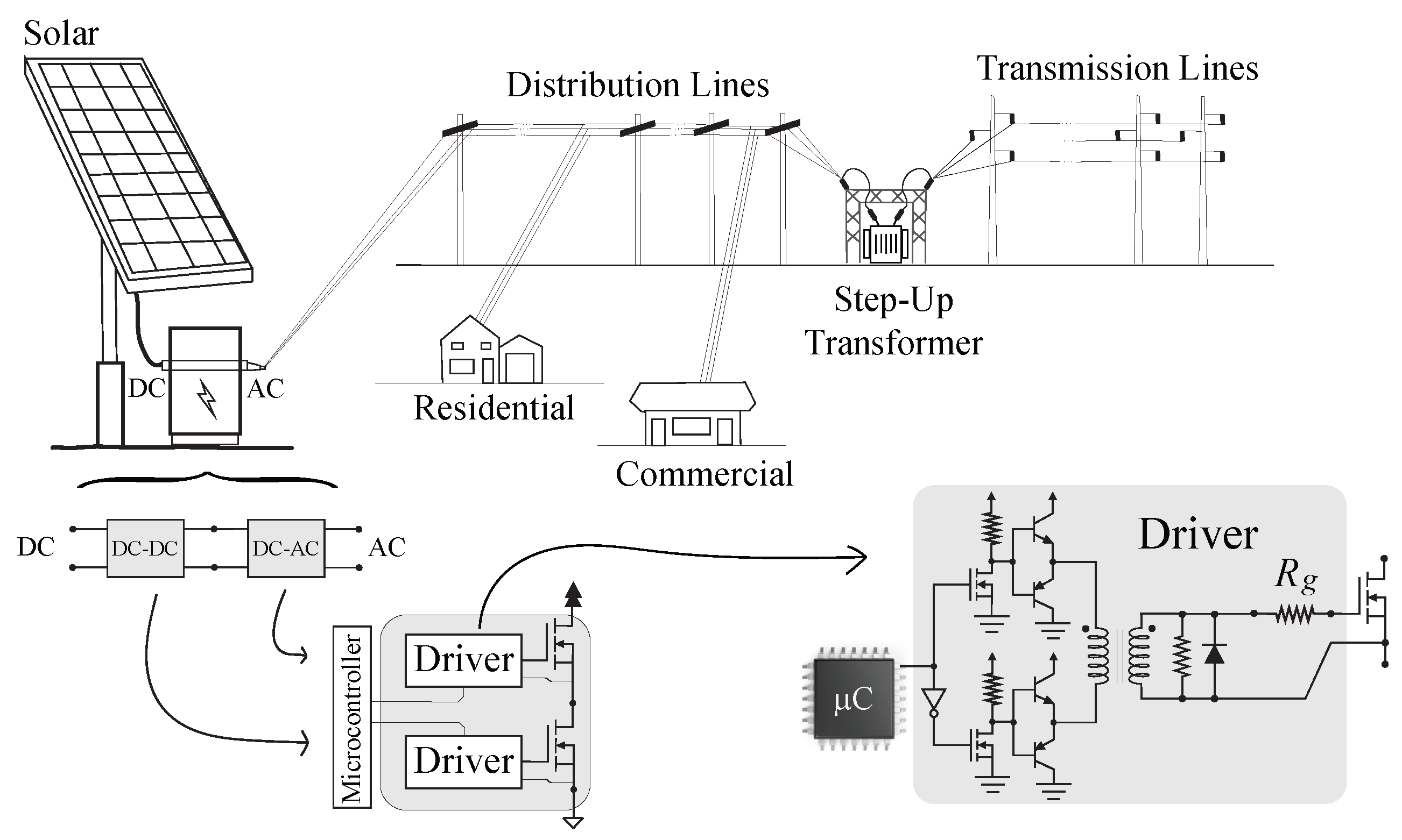
Figure 2.
Circular-economy pathways for PV systems, illustrating material flow from resource extraction through design, manufacturing, use, and end-of-life options including reuse, remanufacturing, recycling, and disposal.
Figure 2.
Circular-economy pathways for PV systems, illustrating material flow from resource extraction through design, manufacturing, use, and end-of-life options including reuse, remanufacturing, recycling, and disposal.
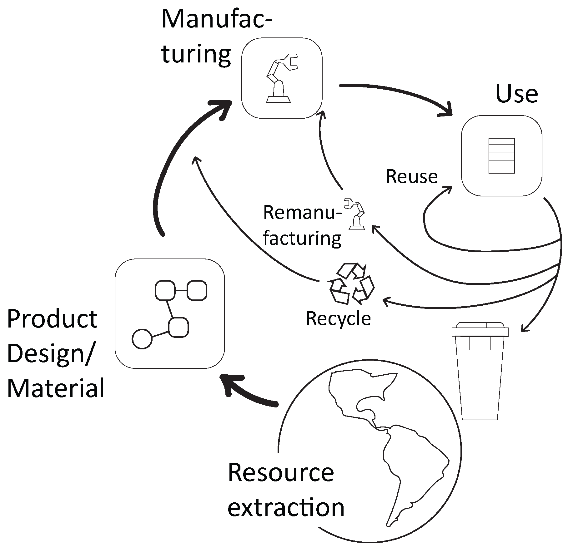
Figure 3.
Impact of gate resistance on MOSFET turn-on behavior. Smaller values generate higher overshoot and ringing (indicating greater switching stress) while larger values yield more damped, lower-stress transients (where is the microcontroller voltage and is the MOSFET gate-source voltage).
Figure 3.
Impact of gate resistance on MOSFET turn-on behavior. Smaller values generate higher overshoot and ringing (indicating greater switching stress) while larger values yield more damped, lower-stress transients (where is the microcontroller voltage and is the MOSFET gate-source voltage).
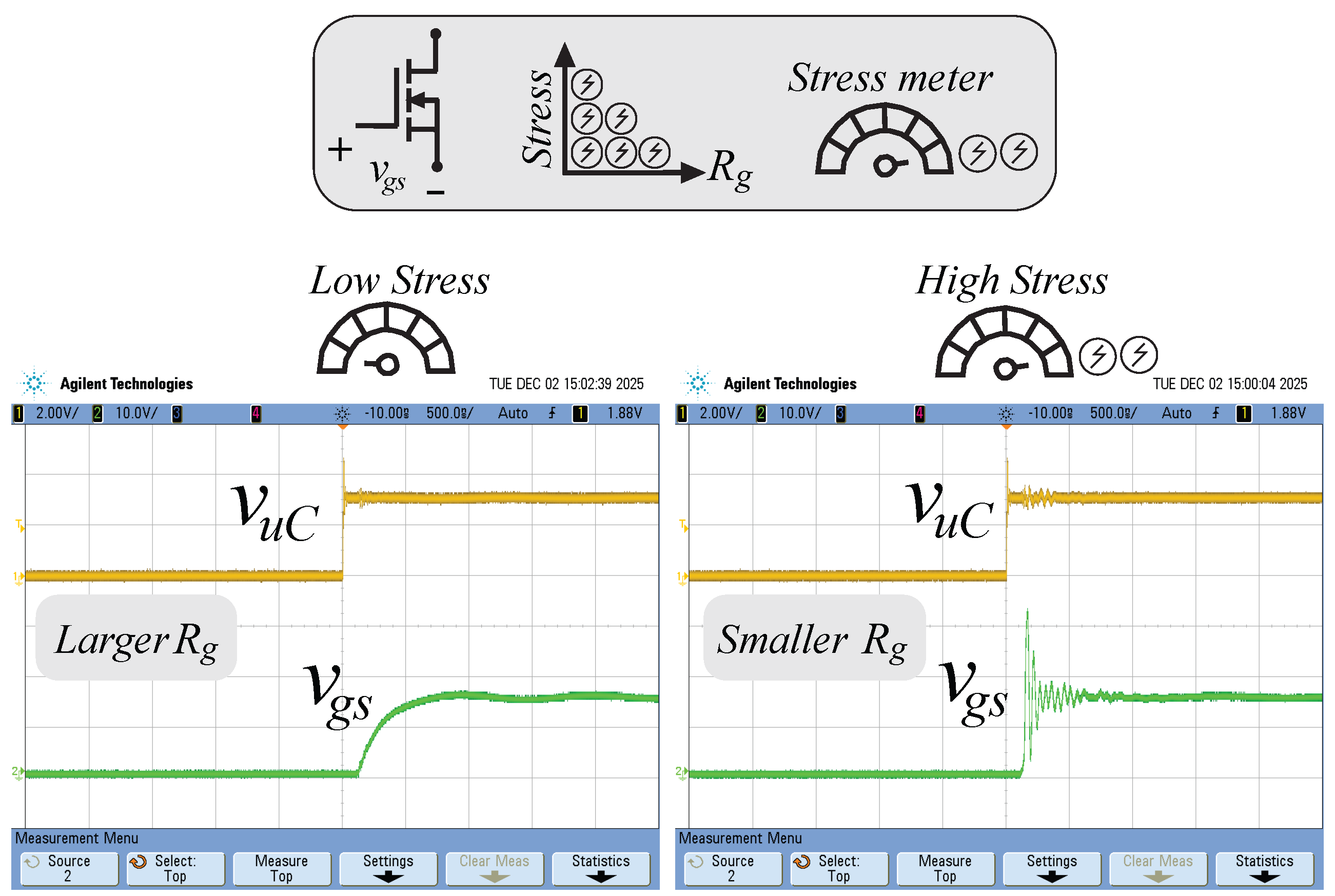
Figure 4.
(Top) Median (thick gray line) and mean (thin black line) annual degradation rates of photovoltaic (PV) modules across four major climate categories. (Bottom) Normalized PV power output over a 30-year service life assuming a compound annual degradation rate of 1.5%, illustrating the long-term decline in available power.
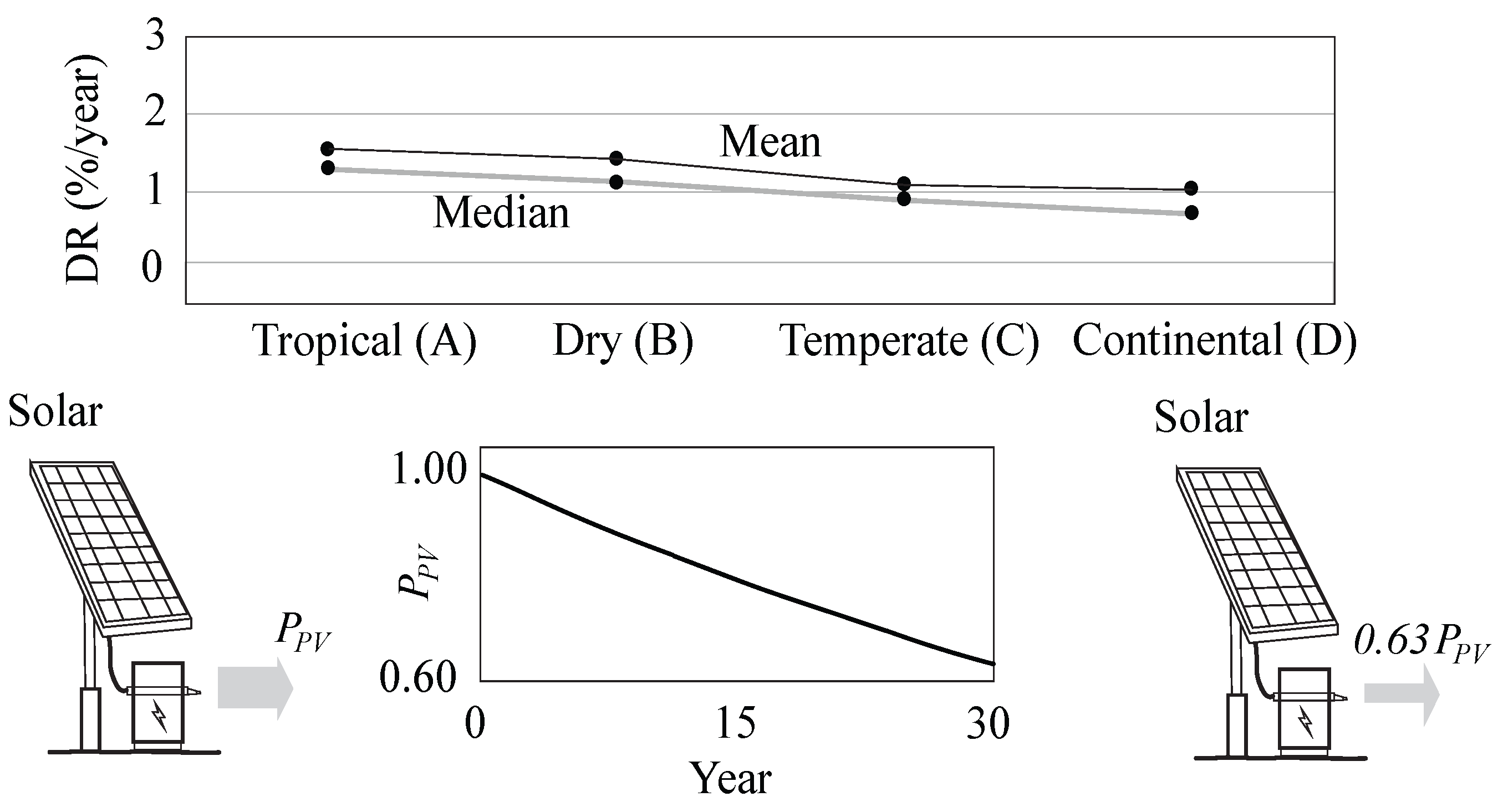
Figure 5.
PV module degradation trajectories from year 0 to 50, combined with an illustration of gate-driver tuning. After the nominal 30-year lifespan, different degradation rates (1%, 3%, 9%, and 20%/year) are shown, and a tunable gate resistance is highlighted as a means to reduce stress on the power switch during late-life operation.
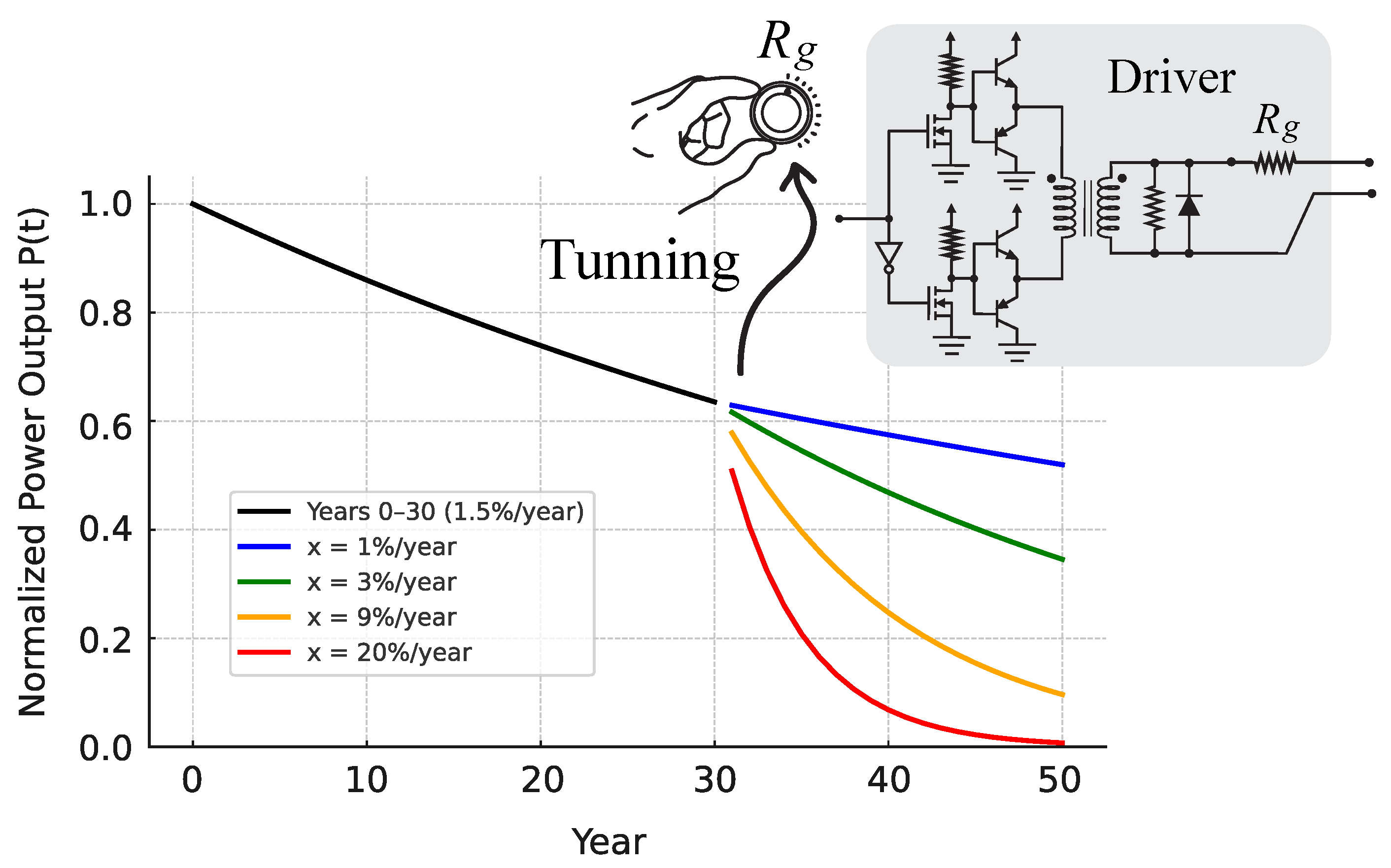
Figure 6.
Impact of gate-resistance retuning on switching behavior. Coordinated adjustment of and enables significant reduction in electrical stress on the power switch, thereby extending component lifetime without increasing overall switching losses.
Figure 6.
Impact of gate-resistance retuning on switching behavior. Coordinated adjustment of and enables significant reduction in electrical stress on the power switch, thereby extending component lifetime without increasing overall switching losses.
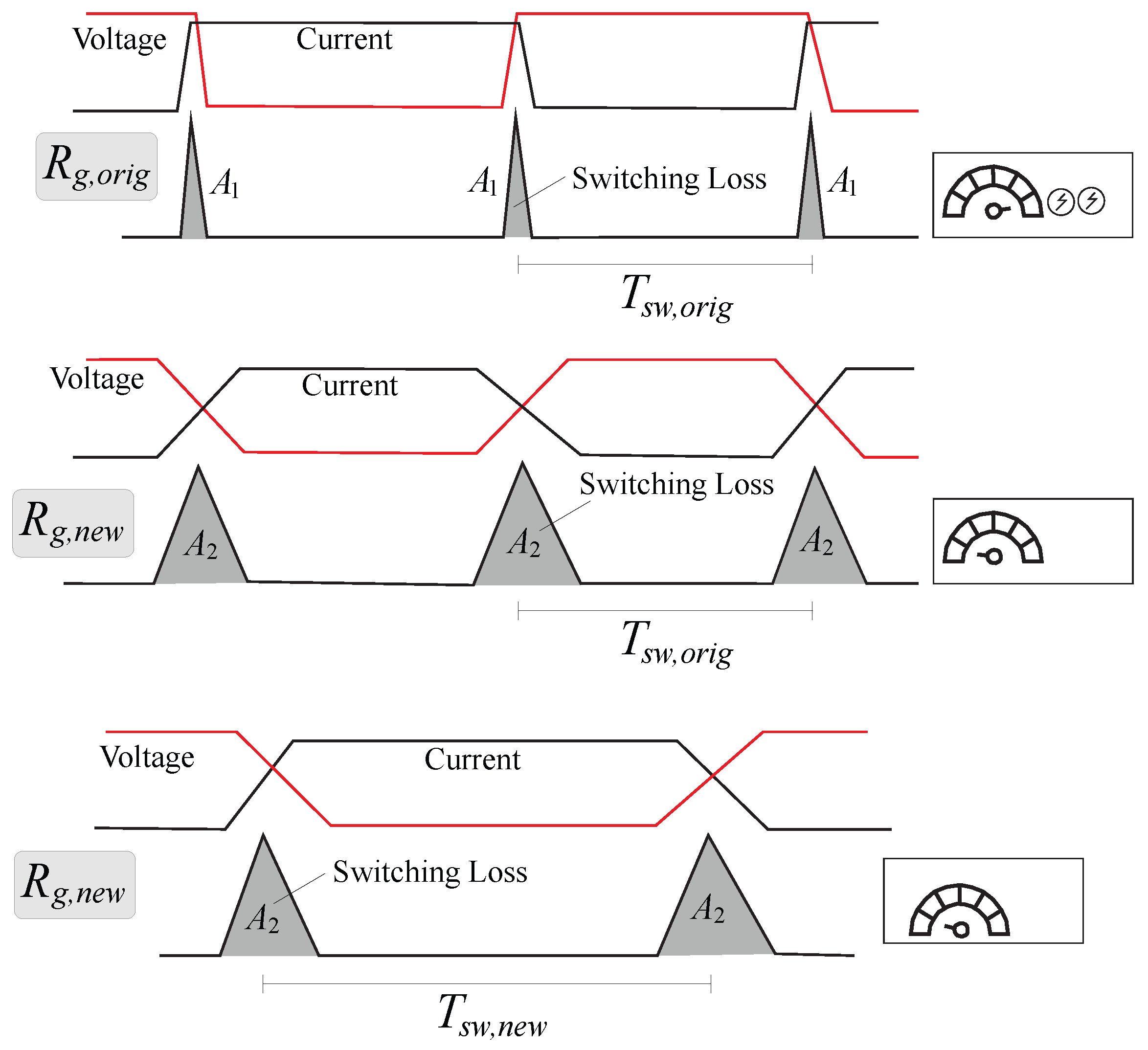
Figure 7.
Heatmap of the normalized lifetime gain for as a function of the switching–frequency ratio and the total number of thermo–electrical cycles. The vertical axis is logarithmic to match typical power–cycling lifetime ranges (– cycles). Warmer colors correspond to higher lifetime gain.
Figure 7.
Heatmap of the normalized lifetime gain for as a function of the switching–frequency ratio and the total number of thermo–electrical cycles. The vertical axis is logarithmic to match typical power–cycling lifetime ranges (– cycles). Warmer colors correspond to higher lifetime gain.
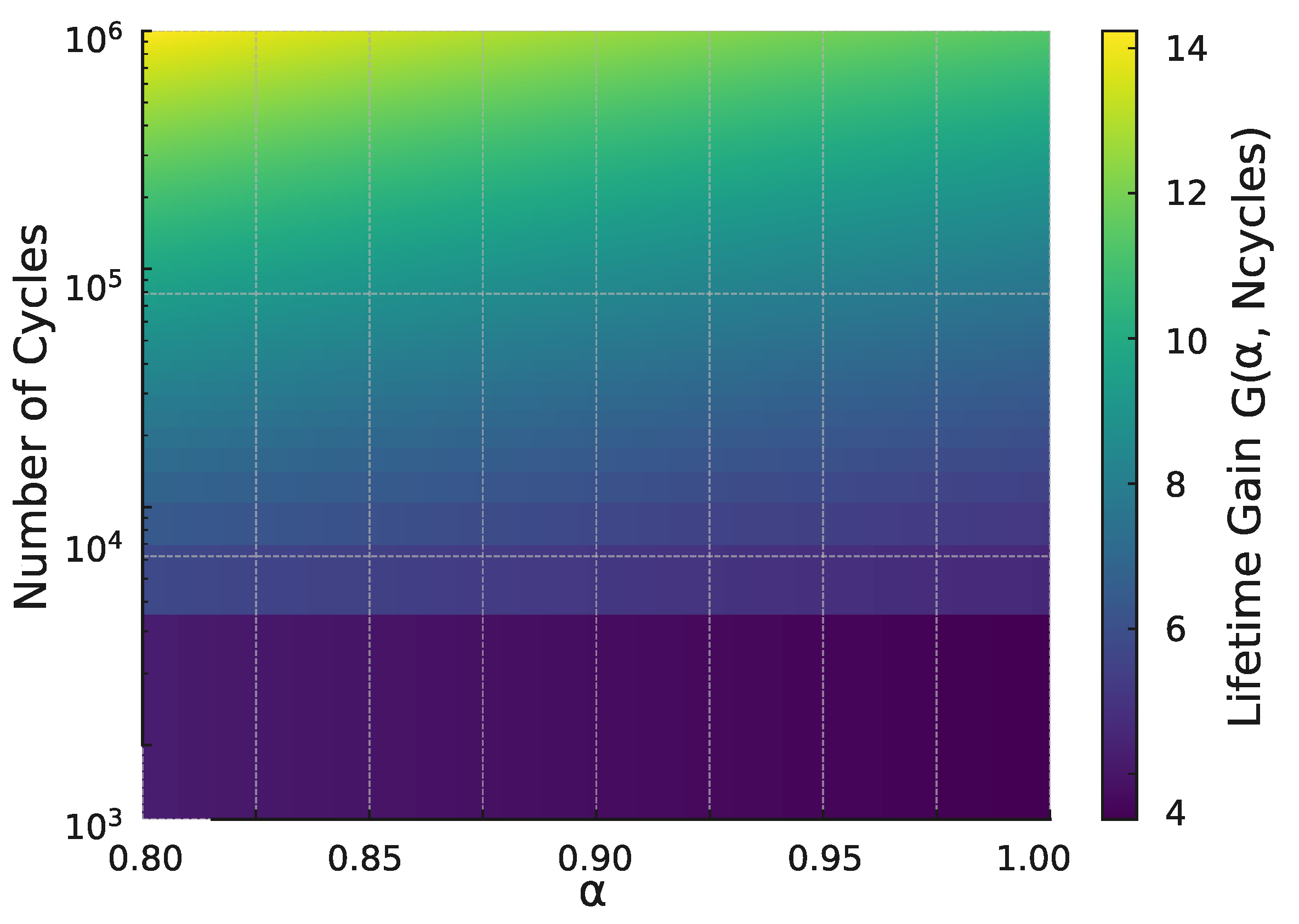
Figure 8.
(a) Test Circuit Diagram. (b) Photo of the implemented re-tuned driver board with major components.
Figure 8.
(a) Test Circuit Diagram. (b) Photo of the implemented re-tuned driver board with major components.
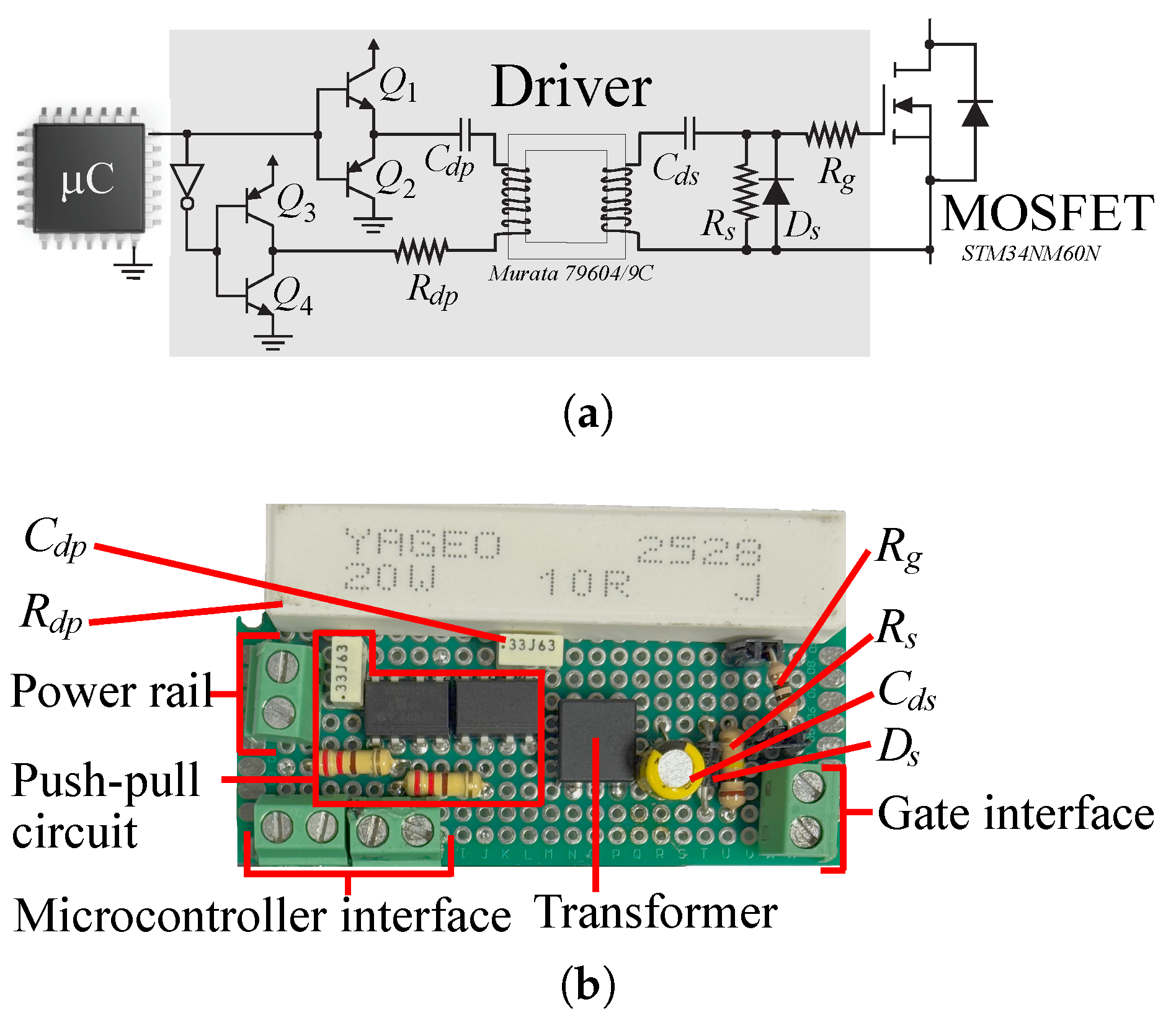
Figure 9.
Gate-Source Voltage (), Drain-Source Voltage () and Drain Current () for (a) , (b) , (c) .
Figure 9.
Gate-Source Voltage (), Drain-Source Voltage () and Drain Current () for (a) , (b) , (c) .
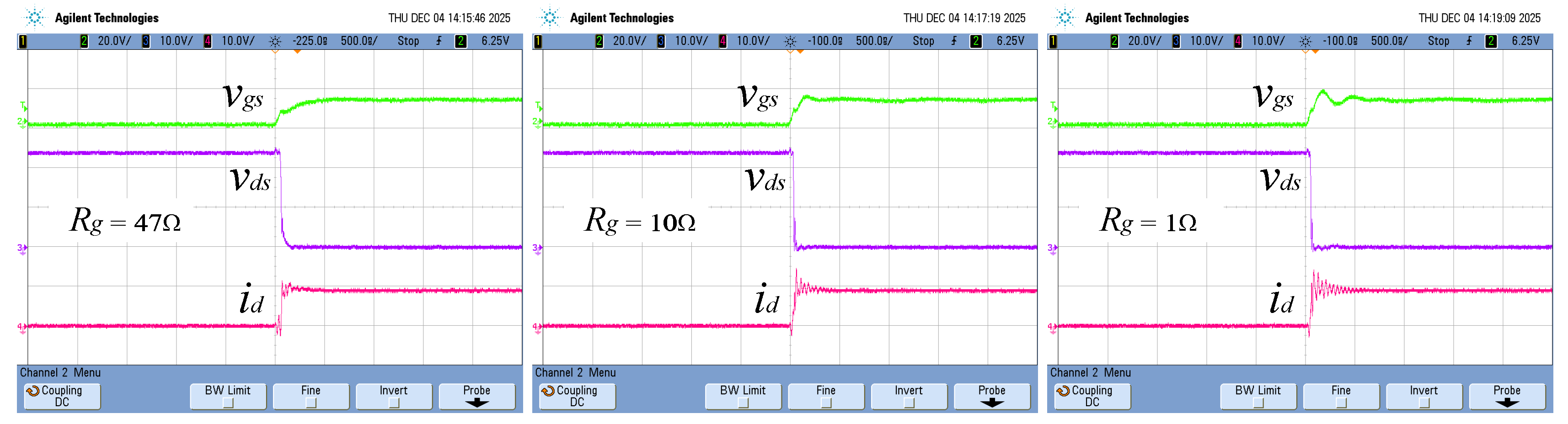
Figure 10.
Drain-Source Voltage (), Drain Current () and Power Loss for (a) , (b) , (c) .
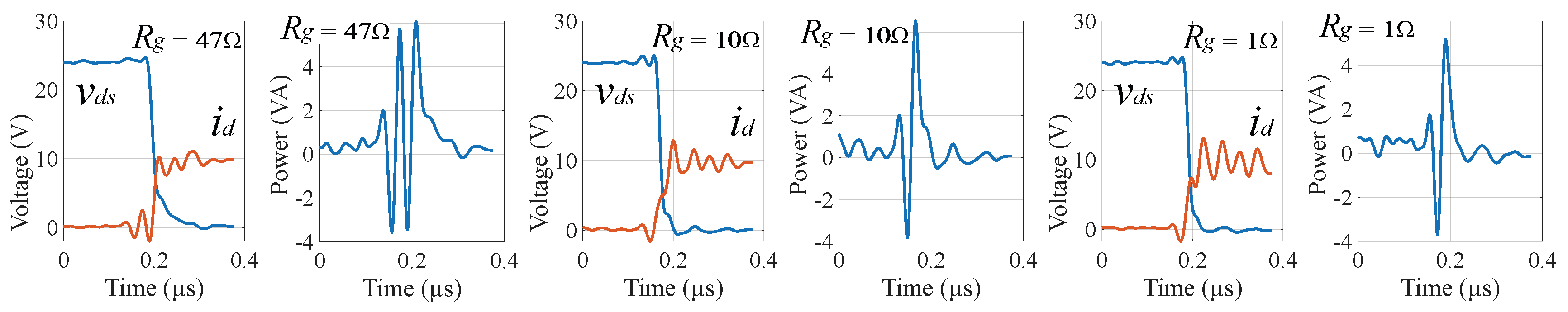

Table 1.
Component Values
| Component | Value |
|---|---|
| 0.33 F | |
| 10 (20 W) | |
| 22 F | |
| 100 k |
Disclaimer/Publisher’s Note: The statements, opinions and data contained in all publications are solely those of the individual author(s) and contributor(s) and not of MDPI and/or the editor(s). MDPI and/or the editor(s) disclaim responsibility for any injury to people or property resulting from any ideas, methods, instructions or products referred to in the content. |
© 2025 by the authors. Licensee MDPI, Basel, Switzerland. This article is an open access article distributed under the terms and conditions of the Creative Commons Attribution (CC BY) license (http://creativecommons.org/licenses/by/4.0/).
Copyright: This open access article is published under a Creative Commons CC BY 4.0 license, which permit the free download, distribution, and reuse, provided that the author and preprint are cited in any reuse.


