Submitted:
03 December 2025
Posted:
03 December 2025
You are already at the latest version
Abstract
In this paper, the leakage inductances influences of integrated-transformer are investigated for an input-series flyback converter, in which each input-series circuit is based on the single-switch flyback topology. First, configuration of this converter is introduced, and a novel multiple inductors coupling model is proposed for its flyback integrated-transformer. Second, operational process of this converter is analyzed considering the leakage inductances between primary and secondary windings of its integrated-transformer. Third, influences of these leakage inductances are analyzed, on this basis, the essential design considerations of flyback integrated-transformer are summarized. Finally, an experimental prototype of this input-series converter is built, based on which, the analysis is verified by the experimental comparisons among three flyback integrated-transformers with various windings layouts.
Keywords:
flyback integrated-transformer
; input-series
; leakage inductances
; windings layout
1. Introduction
With the continuous development of power electronics technique, more and more converters with medium or high input voltages (≥1000V) are needed in various industry applications, especially in the renewable energy and transportation applications [1,2,3]. In these converters, the high voltage issue of each component is the most urgent problem to be solved. The input-series structure is an valid scheme to solve the high voltage problem in the converters with medium or high input voltages, and voltage stress of each component in these converters can be reduced substantially as long as the input voltage sharing of each input-series circuit is achieved [4,5].
Generally, there are two basic input-series structures, one is the output-parallel strategy, as shown in Figure 1a, and the other one is the output-series strategy, as shown in Figure 1b. In addition to the input voltage sharing, the output voltage and current sharing should also be ensured in these two kinds input-series converters respectively [5,6,7]. In the past years, many voltage or current sharing strategies have been implemented, and a good voltage or current sharing effect can be achieved for each converter [7,8,9,10,11,12]. These two basic input-series structures can be applied in various power applications, provided the suitable circuit topology is adopted in each input-series circuit. However, their output connections will become more complex when the multiple-output is required, so these two basic input-series structures are not suitable to be applied in the multiple-output applications.
Aiming at the multiple-output applications, the output-independent strategy is applied in the input-series converters, as shown in Figure 1c. The input voltage sharing effect of these converters will be serious when the energies transferring through various output circuits are unbalanced, so the output-independent strategy can only be adopted in the applications when the energies transferring through different output circuits are balanced [13,14,15,16].
In addition to the output-parallel, output-series and output-independent strategies, the transformer-integration strategy can also be applied in the input-series converters, as shown in Figure 1d, where all input-series circuits enjoy a common integrated-transformer, so the output circuits can be made in secondary sides of this integrated-transformer conveniently [17,18,19,20,21,22]. In these input-series transformer-integration (ISTI) converters, the natural input voltage sharing can be achieved, provided all input-series circuits are operating synchronously. The transformer-integration strategy can also be applied in various power applications, as long as the suitable circuit topology is adopted in each input-series circuit. Compared to the output-parallel or output-series strategy, the transformer-integration strategy is much more suitable to be applied when the multiple output circuits are required, which is a conventional requirement in the low power applications.
Recently, the ISTI flyback converters have been investigated systematically in the multiple-output low power applications [18,20]. The investigations show that: input voltage sharing of the ISTI flyback converters can be achieved through the coupling relationships of primary windings in the integrated-transformer, and the input voltage sharing effect cannot be affected by the components in secondary sides of the integrated-transformer. In these ISTI flyback converters, there are multiple primary and secondary windings in each integrated-transformer, influences of the coupling relationships between arbitrary two windings should be clarified, based on which, layouts of these windings can be determined in the design process. Presently, influences of the coupling relationships among primary windings have been clarified, as well as the coupling relationships among secondary windings. However, influences of the coupling relationships between primary and secondary windings have not been clarified.
In each flyback integrated-transformer, there are multiple primary and secondary windings, so numerous leakage inductances are needed to represent the coupling between each primary winding and each secondary winding, which cannot be realized in the existing model of the flyback integrated-transformer. Therefore, a novel multiple inductors coupling model is proposed for this flyback integrated-transformer in this paper, through which the coupling relationships between primary and secondary windings are analyzed, and essential design considerations of the flyback integrated-transformer are summarized.
The remainder of this paper is organized as follows. In Section 2, the ISTI flyback converter and multiple inductors coupling model of its integrated-transformer are introduced. In Section 3, operational process of this converter is analyzed, where the leakage inductances between primary and secondary windings are considered. In Section 4, the leakage inductances influences are analyzed, based on which, essential design considerations of the flyback integrated-transformer are summarized. In Section 5, the analysis is verified by the experimental comparisons among three flyback integrated-transformers with various windings layouts. In Section 6, the conclusion is given.
2. ISTI Flyback Converter and Its Integrated-Transformer
2.1. Configuration of the ISTI Flyback Converter
Figure 2 shows configuration of the ISTI flyback converter, where each input-series circuit is based on the single-switch flyback topology, Vi and Ii are the input voltage and input current, Vi-1, …, Vi-N are input voltages of the N (N≥2) input-series circuits, Vo-1, …, Vo-n and Io-1, …, Io-n are output voltages and output current of the n (n≥1) output-independent circuits.
In the input-series circuits, there are the identical components and parameters, including the input filter capacitors (Ci-1=…=Ci-N), the switches (S1, …, SN), the turns number (Np-1=…=Np-N) and the self-inductances (Lp-1=…=Lp-N) of primary windings (Wp-1, …, Wp-N) in the integrated-transformer (T), and the absorbing circuits (R1=…=RN, C1=…=CN and D1, …, DN).
In the output-independent circuits, the turns number (Ns-1, …, Ns-n) of secondary windings (Ws-1, …, Ws-n) in T, as well as the output rectifier diodes (Do-1, …, Do-n) and output filter capacitors (Co-1, …, Co-n) are designed according to the special output requirements.
2.2. Multiple Inductors Coupling Model of Flyback Integrated-Transformer
In [18,20], the input voltage sharing effects of various flyback ISTI converters are investigated. These investigations can be concluded as follows.
(1) The N primary windings of T are considered as a coupled-inductor, by which input voltage sharing of the N input-series circuits is ensured naturally, provided all switches are turning synchronously. The input voltage sharing will be achieved more efficiently as the coupling coefficients of this coupled-inductor increase.
(2) Due to the inevitable parameters errors, the absolute synchronous turning of S1, …, SN cannot be realized, so the input voltage differences occur among various input-series circuits, which will increase as the parameters errors increase. The input voltage differences can be reduced through special design of the key parameters, especially the input filter capacitances (Ci-1, …, Ci-N).
(3) Input voltage sharing effects of the N input-series circuits cannot be affected by the components in secondary sides of T. Influences of the coupling relationships among secondary windings of T are similar to those in the other traditional flyback converters with multiple output circuits, which are not the specific problems in each ISTI flyback converter.
From the above conclusions, it can be obtained that: the flyback integrated-transformer is a main device, so its design and manufacturing are very important.
In the integrated-transformer, there are N primary windings and n secondary windings, so influences of the coupling relationships among these windings should be clarified, on this basis, layouts of these windings can be determined in the design process. In the previous investigations, influences of the coupling relationships among primary windings have been clarified, as well as the coupling relationships among secondary windings. However, influences of the coupling relationships between primary and secondary windings have not been clarified.
Generally, the coupling between arbitrary two windings should be represented by at least one leakage inductance, so N×n leakage inductances are needed to represent the coupling between N primary windings and n secondary windings, which cannot be realized in the existing model of the flyback integrated-transformer.
To overcome the shortcomings of the existing model, a novel multiple inductors coupling model is proposed for this flyback integrated-transformer, as shown in Figure 3, through which influences of the coupling relationships between primary and secondary windings are expected to be clarified. This novel model is introduced as follows.
(1) Influences of the coupling relationships among secondary windings are not considered. To simplify the analysis, the equivalent single secondary winding (Ws-1) is adopted to represent the n secondary windings.
(2) The single secondary winding (Ws-1) is divided into N identical parts (Ws-11, …, Ws-1N), and they are made as the secondary windings of the ideal transformers (Ti-1, …, Ti-N). Ti-1, …, Ti-N are connected in parallel in the secondary sides, where their turns ratio are identical (Np-1/Ns-1), and Do-11, …, Do-1N stand for the output rectifier diodes.
(3) A coupled-inductor (Lp-1=…=Lp-N) is adopted to represent the coupling relationships among the N primary windings.
(4) The leakage inductances (Llk-1, …, Llk-N) are adopted to represent the coupling relationships between the N primary windings (Wp-1, …, Wp-N) and the equivalent single secondary winding (Ws-1) respectively.
3. Operational Process of ISTI Flyback Converter Considering the Leakage Inductances
Based on the model in Figure 3, operational process of the ISTI flyback converter is analyzed as follows. To simplify the analysis, the following conditions are assumed: 1) this converter operates in discontinuous current mode (DCM); 2) this converter is composed of two input-series circuits (N=2) and single output circuit (n=1); 3) in addition to the integrated-transformer, all devices in this converter are ideal; 4) the asynchronous turning of S1 and S2 is not considered; 5) the input voltage differences between two input-series circuits are not considered (Vi-1=Vi-2=Vi/2); and 6) C1, C2 and Co-1 are large enough, so the fluctuations of their voltages (VC1, VC2 and Vo-1) are ignored. During each switching period, there are the following four stages, where the main waveforms in each period are shown in Figure 4, and the equivalent circuit in each stage is shorn in Figure 5.
Stage 1 (t0~t1): At t0, S1 and S2 are turned on. After t0, the coupled-inductor (Lp-1, Lp-2) is charged by the input voltages, so its current increases. In the absorbing circuits, D1 and D2 are turning off, C1 and C2 are discharged through R1 and R2 respectively. In the output circuits, Do-11 and Do-12 are turning off, and Io-1 is only provided by Co-1. In this stage, the voltages in primary or secondary side of Ti-1 and Ti-2 are: Vp-1=Vi-1=Vi/2, Vp-2=Vi-2=Vi/2 and Vs-11=Vs-12=Ns-1Vi/2Np-1. At t1, the current of these inductors increases to the peak value during the whole period, as shown in Equation (1).
where ip-1 (or ip-2) and ilk-1 (or ilk-2) are the current of Lp-1 (or Lp-2) and Llk-1 (or Llk-2) respectively; Lp-es=2(1+k12)Lp-1 is the equivalent series inductance of Lp-1 and Lp-2; k12 is the coupling coefficient between Lp-1 and Lp-2; and Llk-1 (or Llk-2) is much smaller than Lp-es, which are not considered here.
Stage 2 (t1~t2): At t1, S1 and S2 are turned off, and their voltages (VS1 and VS2) increase immediately to Vi-1+VC1 and Vi-2+VC2 respectively. Duration of these processes are very small, which are not considered here.
After t1, Do-11 and Do-12 are turning on, and the energies stored in Lp-1 and Lp-2 are transferred to the loads through Ti-1 and Ti-2 respectively. In the absorbing circuits, D1 and D2 are turning on, and the energies stored in Llk-1 and Llk-2 are transferred into C1 and C2 respectively. In this stage, Vs-11=Vs-12= -Vo-1 and Vp-1=Vp-2= -Np-1Vo-1/Ns-1, moreover, the expressions of ip-1 (or ip-2) and ilk-1, ilk-2 can be obtained in Equations (2) and (3) respectively.
where Lp-ep=(1+k12)Lp-1/2 is the equivalent parallel inductance of Lp-1 and Lp-2.
At the end of this stage, ilk-1 and ilk-2 decrease to zero, and then, D1 and D2 are turned off accordingly.
Stage 3 (t2~t3): At t2, ilk-1=ilk-2=0. After t2, C1 (or C2) is still discharged through R1 (or R2), and the decreasing of ip-1 (or ip-2) is continuous. In this stage, Vp-1, Vp-2 and Vs-11, Vs-12 are fixed, however, VS1 and VS2 are changed into Vi-1+Vp-1 and Vi-2+Vp-2 respectively.
Stage 4 (t3~t4): At t3, ip-1=ip-2=0. After t3, Do-11 and Do-12 are turning off, Vp-1=Vp-2=0, Vs-11=Vs-12=0, VS1=Vi-1=Vi/2, VS2=Vi-2=Vi/2, and Io-1 is only provided by Co-1.
At t4, S1 and S2 are turned on again. After t4, this converter will operate in the next period.
4. Design Considerations of Integrated-Transformer Based on the Leakage Inductances
According to the operational process, the influences of leakage inductances (Llk-1, Llk-2) between the primary windings (Wp-1, Wp-2) and the equivalent single secondary winding (Ws-1) are analyzed in this section, based on which, the essential design considerations of this flyback integrated-transformer are summarized.
4.1. Analysis of the Leakage Inductances Influences
For the ISTI flyback converter, the input voltage sharing of each input-series circuit is achieved by the coupling of primary windings in the integrated-transformer, and this input voltage sharing process occurs when all switches are turning on. During the whole switching period, the maximum voltages of S1 and S2 are equal to Vi-1+VC1 and Vi-2+VC2 respectively. Therefore, the voltage sharing effect of S1 and S2 cannot be ensured even if a good input voltage sharing effect has been achieved (Vi-1=Vi-2=Vi/2).
In stage 1, S1 and S2 are turning on, and the coupling relationships of two primary windings (Wp-1, Wp-2) are represented by the coupled-inductor (Lp-1, Lp-2). The leakage inductance Llk-1 (or Llk-2) is much smaller than the equivalent series inductance (Lp-es) of this coupled-inductor, so the input voltage sharing process in this stage have almost no relationship with Llk-1 (or Llk-2). In stage 3 and stage 4, the current of Llk-1 (or Llk-2) is zero, so there is almost no influence caused by Llk-1 (or Llk-2) in these stages.
Therefore, the analysis of leakage inductances (Llk-1, Llk-2) influences is implemented in stage 2 as follows, where the simplified equivalent circuit of the ISTI flyback converter in stage 2 is shown in Figure 6.
From operational process of the ISTI flyback converter, it can be obtained that: during the whole switching period, C1 and C2 are discharged through R1 and R2 respectively. Accordingly, the energies decreasing of C1 and C2 during each switching period can be estimated in Equation (4).
where T is the switching period.
It can be obtained from Equation (4) that: when the parameters (R1=R2 and C1=C2) are fixed, the power losses caused by the absorbing circuit in each input-series circuit is determined by VC1 (or VC2), which will increase as VC1 (or VC2) increases.
In stage 2, the current of Llk-1 and Llk-2 will decrease to zero, and their current decreasing durations can be obtained from Equation (3), as shown in Equation (5).
From Equations (3) and (5), the energies increasing of C1 and C2 in stage 2 can be estimated in Equation (6), where Tlk-1 (or Tlk-2) is much smaller than T, so the energies releasing of R1 and R2 are not considered in the estimations.
During the whole switching period, it is required that: EC1+=EC1- and EC2+=EC2- Therefore, the relationships in Equation (7) can be obtained from Equations (4) and (6).
In stage 2, the energies stored in Llk-1 and Llk-2 are absorbed by C1 and C2, so it should be achieved that: VC1>Np-1Vo-1/Ns-1 and VC2>Np-1Vo-1/Ns-1. Moreover, it is considered that: ilk-1(t1)=ilk-2(t1), as shown in Equation (1). Therefore, it can be obtained from Equation (7) that: when the parameters (R1=R2 and C1=C2) are fixed, VC1 and VC2 are determined by Llk-1 and Llk-2, which will increase as Llk-1 and Llk-2 increase respectively.
4.2. Essential Design Considerations of Flyback Integrated-Transformer
From the leakage inductances influences, essential design considerations of the flyback integrated-transformer can be summarized from two aspects: 1) voltage sharing effects of the switches (S1, S2); and 2) power losses caused by the absorbing circuit in each input-series circuit. They are summarized as follows.
(1) The maximum voltages of S1 and S2 are equal to Vi-1+VC1 and Vi-2+VC2 respectively. When a good input voltage sharing effect is achieved (Vi-1=Vi-2=Vi/2) after optimal design of the coupling between primary windings, the voltage sharing effect of C1 and C2 should be considered specially. As shown in Equation (7), VC1 and VC2 are determined by the leakage inductances (Llk-1 and Llk-2), and VC1=VC2 can be achieved when Llk-1=Llk-2. Therefore, to achieve a good voltage sharing effect of S1 and S2, the difference between Llk-1 and Llk-2 should be suppressed, and Llk-1=Llk-2 is expected to be achieved especially.
(2) The energies stored in Llk-1 and Llk-2 are transferred into C1 and C2 in stage 2, and these energies are released through R1 and R2 respectively, so these energies should be reduced, which is similar to the other flyback converter. As shown in Equations (4) and (7), the power losses caused by the absorbing circuits will increase as VC1 (or VC2) increases, and VC1 (or VC2) will increase as Llk-1 (or Llk-2) increases. Therefore, the leakage inductances (Llk-1 and Llk-2) should be reduced to decrease the power losses caused by the absorbing circuits.
5. Experimental Verifications
5.1. Experimental Prototype
To verify the aforementioned analysis, a 1000 V experimental prototype of the ISTI flyback converter is built, as shown in Figure 7. This experimental prototype is composed of two input-series circuits (N=2) and two output-independent circuit (n=2), and each input-series circuit is based on the single-switch flyback topology. The main components and parameters of this experimental prototype are shown in Table 1.
Based on this prototype, three flyback integrated-transformers (T1, T2 and T3) with various typical layout schemes of the primary windings (Wp-1, Wp-2) are designed for the experimental comparisons. Windings layouts of T1, T2 and T3 can be obtained from their cross sections, as shown in Figure 8, in which only half of the cross section is given in each illustration, and the number marked on each turn represents its manufacturing sequence.
In each flyback integrated-transformer, the secondary windings (Ws-1, Ws-2) are connected in parallel, and they are manufactured intensively to improve their coupling relationship. Layouts of Ws-1 and Ws-2 are identical in T1, T2 and T3, which are not given specially in Figure 8. Moreover, the other common features of these integrated-transformers are shown in Table 2, and layout schemes of their primary windings (Wp-1, Wp-2) are explained as follows.
In T1, Wp-1 and Wp-2 are connected in parallel. The four layers of Wp-1 and Wp-2 are divided into two parts, where Ws-1 and Ws-2 are rounded in the middle of these two parts.
In T2, the layer-by-layer windings layout is selected for Wp-1 and Wp-2. The two layers of Wp-1 (or Wp-2) are divided into two parts, where Ws-1 and Ws-2 are rounded in the middle of these two parts. The two layers of Wp-1 are rounded near Ws-1 and Ws-2, and the two layers of Wp-2 are rounded in the innermost and outermost layers respectively.
In T3, Wp-1 and Wp-2 are connected in parallel, and they are made in the inner four layers. Ws-1 and Ws-2 are made in the outer layers.
The main parameters of these integrated-transformers are measured by the LCR meter (Tonghui/TH2826), including the coupling coefficient (k12) and the leakage inductances (Llk-1, Llk-2). The measuring results are shown in Table 3. It can be obtained that: 1) a high coupling coefficient has been achieved in each integrated-transformer; 2) in T1 (or T3), there is almost no difference between Llk-1 and Llk-2, however, there is an obvious difference between Llk-1 and Llk-2 in T2; and 3) in T3, Llk-1 (or Llk-2) is much larger than that in T1 (or T2).
According to the aforementioned analysis, the experimental results can be expected that: 1) a good input voltage sharing effect will be achieved for this experimental prototype when any one of the integrated-transformers is adopted; 2) when T1 (or T3) is adopted, there is almost no voltage difference between C1 and C2, so a good voltage sharing effect will be achieved between S1 and S2; 3) when T1 (or T2) is adopted, the voltages of C1 and C2 will be lower than those when T3 is adopted; and 4) when T1 (or T2) is adopted, the power losses caused by the absorbing circuits will be much lower, so the efficiency of the experimental prototype will be higher than that when T3 is adopted.
5.2. Experimental Results
The three flyback integrated-transformers (T1, T2 and T3) are used in this experimental prototype one by one, and the main experimental results are shown in Figure 9, Figure 10, Figure 11 and Table 4.
Figure 9 shows the main experimental waveforms when T1 is used, including the driving (vgs1), voltage (vds1) and current (iS1) of S1, the driving (vgs2), voltage (vds2) and current (iS2) of S2, the input voltages (Vi-1, Vi-2) of two input-series circuits, and the voltages (VC1, VC2) of two capacitors in the absorbing circuits. Figure 10 and Figure 11 show the main experimental waveforms when T2 and T3 are used. It can be seen from these waveforms that: a good input voltage sharing effect has been achieved for this experimental prototype when any one of the integrated-transformers is adopted.
Table 4 shows the main measuring results when T1, T2 and T3 are used one by one, including the voltages (VC1, VC2) of two capacitors in the absorbing circuits, and the efficiency (η) of this experimental prototype.
It can be obtained from Figure 9d, Figure 10d, Figure 11d and Table 4 that: 1) when T1 is used, there is almost no voltage difference between the two capacitors (C1 and C2) in the absorbing circuits; 2) when T2 is used, an obvious voltage difference (VC2-VC1=9 V) appears between C1 and C2; and 3) when T3 is used, there is almost no voltage difference between C1 and C2, however, voltage of C1 (or C2) is much higher than that when T1 (or T2) is adopted. Moreover, it can also be obtained from Table 4 that: when T1 (or T2) is used, the efficiency of this experimental prototype is higher than that when T3 is adopted.
Therefore, it can be seen that: the analysis of the leakage inductances influences has been verified through the above experimental comparisons.
6. Conclusion
In this paper, influences of the leakage inductances between primary and secondary windings are investigated for the integrated-transformer in an input-series flyback converter, in which each input-series circuit is based on the single-switch flyback topology. To represent the coupling relationship between primary and secondary windings, a novel multiple inductors coupling model is proposed for the flyback integrated-transformer, operational process of this converter and the leakage inductances influences are analyzed based on this model, and the essential design considerations of flyback integrated-transformer are summarized: 1) the difference of various leakage inductances should be suppressed as much as possible to achieve a good voltage sharing effect of the switches in different input-series circuits; and 2) the leakage inductances should be reduced to decrease the power losses of this converter. The investigating results are verified by the experimental comparisons among three flyback integrated-transformers with various windings layouts.
Author Contributions
Conceptualization, S.L. and T.M.; methodology, T.M. and H.B.; software, W.H. and C.L.; validation, S.L. and W.H.; formal analysis, T.M.; investigation, S.L.; resources, T.M.; data curation, S.L. and W.H.; writing—original draft preparation, S.L.; writing—review and editing, S.L. and T.M.; supervision, T.M. and H.B.; project administration, T.M.; funding acquisition, T.M. and C.L. All authors have read and agreed to the published version of the manuscript.
Funding
This research was supported by Heilongjiang Provincial Natural Science Foundation of China (LH2023E107), Program for Young Talents of Basic Research in Universities of Heilongjiang Province (YQJH2024181), and Heilongjiang University Fundamental Research Funds for the Heilongjiang Province Universities (2024-KYYWF-0114).
Data Availability Statement
Data are provided within the manuscript.
Conflicts of Interest
The authors declare no conflicts of interest.
References
- Yoon, D.; Cho, Y.; Bae, S.; Lee, J. An input-series output-series noninverting buck-boost converter for 1500 V dc bus with wide input and output voltage ranges. IEEE Trans. Ind. Electron. 2023, 70, 11231–11241. [Google Scholar] [CrossRef]
- Ren, X.; Xu, Z.; Zhang, Z.; Li, H.; He, M.; Tang, J.; Chen, Q. A 1-kV input SiC LLC converter with split resonant tanks and matrix transformers. IEEE Trans. Power Electron. 2019, 34, 10446–10457. [Google Scholar] [CrossRef]
- Chen, X.; Chen, W.; Yang, X.; Han, Y.; Hao, X.; Xiao, T. Research on a 4000-V-ultrahigh-input-switched-mode power supply using series-connected MOSFETs. IEEE Trans. Power Electron. 2018, 33, 5995–6011. [Google Scholar] [CrossRef]
- Ma, Q.; Huang, Q.; Huang, A. Zero-voltage switching and natural voltage balancing of a 3 kW 1 MHz input-series-output-parallel GaN LLC converter. IEEE Open J. Power Electron. 2024, 5, 1119–1128. [Google Scholar] [CrossRef]
- Ma, D.; Chen, W.; Ruan, X. A review of voltage/current sharing techniques for series-parallel-connected modular power conversion systems. IEEE Trans. Power Electron. 2020, 35, 12383–12400. [Google Scholar] [CrossRef]
- Liu, F.; Zhou, G.; Ruan, X.; Ji, S.; Zhao, Q.; Zhang, X. An input-series-output-parallel converter system exhibiting natural input-voltage sharing and output-current sharing. IEEE Trans. Ind. Electron. 2021, 68, 1166–1177. [Google Scholar] [CrossRef]
- Sha, D.; Guo, Z.; Luo, T.; Liao, X. A general control strategy for input-series-output-series modular dc-dc converters. IEEE Trans. Power Electron. 2014, 29, 3766–3775. [Google Scholar] [CrossRef]
- Qu, L.; Zhang, D.; Zhang, B. Input voltage sharing control scheme for input-series and output-parallel connected dc-dc converters based on peak current control. IEEE Trans. Ind. Electron. 2019, 66, 429–439. [Google Scholar] [CrossRef]
- Wang, L.; Sun, P.; Liang, Y.; Wu, X.; Deng, Q.; Rong, E. Analysis and control design for input-series output-parallel multi-channel inductive power transfer system. IET Power Electron. 2024, 17, 2515–2530. [Google Scholar] [CrossRef]
- Li, S.; Wang, Z.; Yuan, X.; Zhang, Y.; Sun, L.; Wang, K.; Wu, X. A 10 kV/400 V SiC based dc-dc converter with input-series-output-parallel configuration and three-loop control. IEEE Trans. Ind. Appl. 2024, 60, 7013–7029. [Google Scholar] [CrossRef]
- Liu, Y.; Hu, H.; Wang, X.; Gang, Y.; Li, Y. Voltage balance scheme for input-series output-series DAB dc-dc converter with bidirectional power flow. IEEE Trans. Power Electron. 2024, 39, 12030–12034. [Google Scholar] [CrossRef]
- Li, J.; Ma, X.; Xie, Y.; Wang, T.; Shu, Z. Power and voltage balance control strategy of series input parallel output type three-level dual active bridge converter. Trans. China Elect. Soc. 2024, 39, 3082–3092. [Google Scholar]
- Hu, Q.; Zane, R. LED driver circuit with series-input-connected converter cells operating in continuous conduction mode. IEEE Trans. Power Electron. 2010, 25, 574–582. [Google Scholar]
- Yang, W.; Zhang, Z.; Yang, S. A new control strategy for input voltage sharing in input series output independent modular dc-dc converters. J. Power Electron. 2017, 17, 632–640. [Google Scholar] [CrossRef]
- Yang, J.; Zhang, Z.; Sun, K.; Yang, W.; Yang, S.; Li, F.; Yao, Y. Series input multiple outputs flyback auxiliary power supply for input series-output parallel/input series-output series system. IET Power Electron. 2019, 12, 2285–2294. [Google Scholar] [CrossRef]
- Liu, Y.; Liu, X.; Gao, F.; Liu, D.; Wheeler, P. Auxiliary power supply for input-series output-parallel medium-voltage solid state transformers. IEEE Trans. Power Electron. 2023, 38, 7308–7321. [Google Scholar] [CrossRef]
- Choi, S.; Lee, J.; Lee, J. High-efficiency portable welding machine based on full-bridge converter with ISOP-connected single transformer and active snubber. IEEE Trans. Ind. Electron. 2016, 63, 4868–4877. [Google Scholar]
- Meng, T.; Li, C.; Ben, H.; Zhao, J. An input-series flyback auxiliary power supply scheme based on transformer-integration for high-input voltage applications. IEEE Trans. Power Electron. 2016, 31, 6383–6393. [Google Scholar] [CrossRef]
- Meng, T.; Ben, H.; Song, Y.; Li, C. Analysis and design of an input-series two-transistor forward converter for high-input voltage multiple-output applications. IEEE Trans. Ind. Electron. 2018, 65, 270–279. [Google Scholar] [CrossRef]
- Meng, T.; Song, Y.; Wang, Z.; Ben, H.; Li, C. Investigation and implementation of an input-series auxiliary power supply scheme for high-input-voltage low-power applications. IEEE Trans. Power Electron. 2018, 33, 437–447. [Google Scholar] [CrossRef]
- Meng, T.; Ben, H.; Song, Y.; Li, C. Analysis and suppression of the circulating current influence in the input-series auxiliary power supply for high-input-voltage applications. IEEE Trans. Power Electron. 2019, 34, 6533–6543. [Google Scholar] [CrossRef]
- Wang, Y.; Kim, S.; Zhang, H.; Chen, Y.; Park, S. Design and analysis of an input-series quasi-resonant flyback high-voltage SMPS based on an integrated transformer. IET Power Electron. 2022, 15, 1058–1074. [Google Scholar] [CrossRef]
Figure 1.
Input-series structures. (a) Output-parallel strategy. (b) Output-series strategy. (c) Output-independent strategy. (d) Transformer-integration strategy.
Figure 1.
Input-series structures. (a) Output-parallel strategy. (b) Output-series strategy. (c) Output-independent strategy. (d) Transformer-integration strategy.
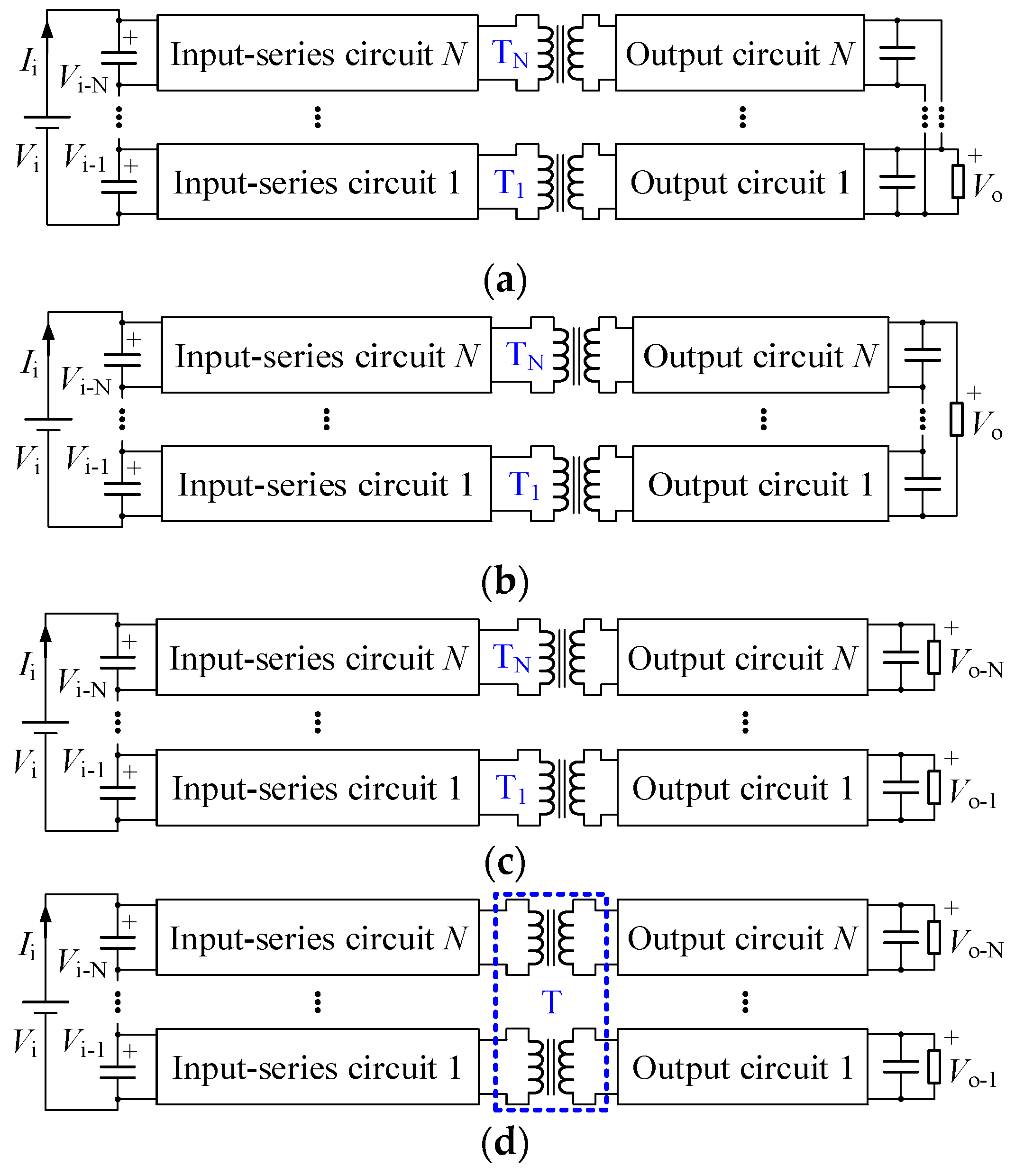
Figure 2.
Configuration of the ISTI flyback converter.
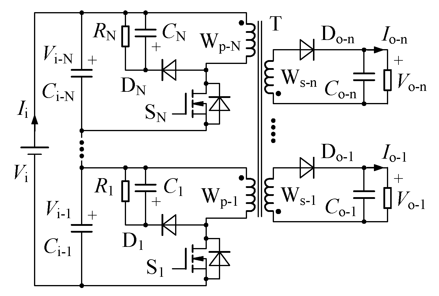
Figure 3.
Multiple inductor coupling model of the flyback integrated-transformer.
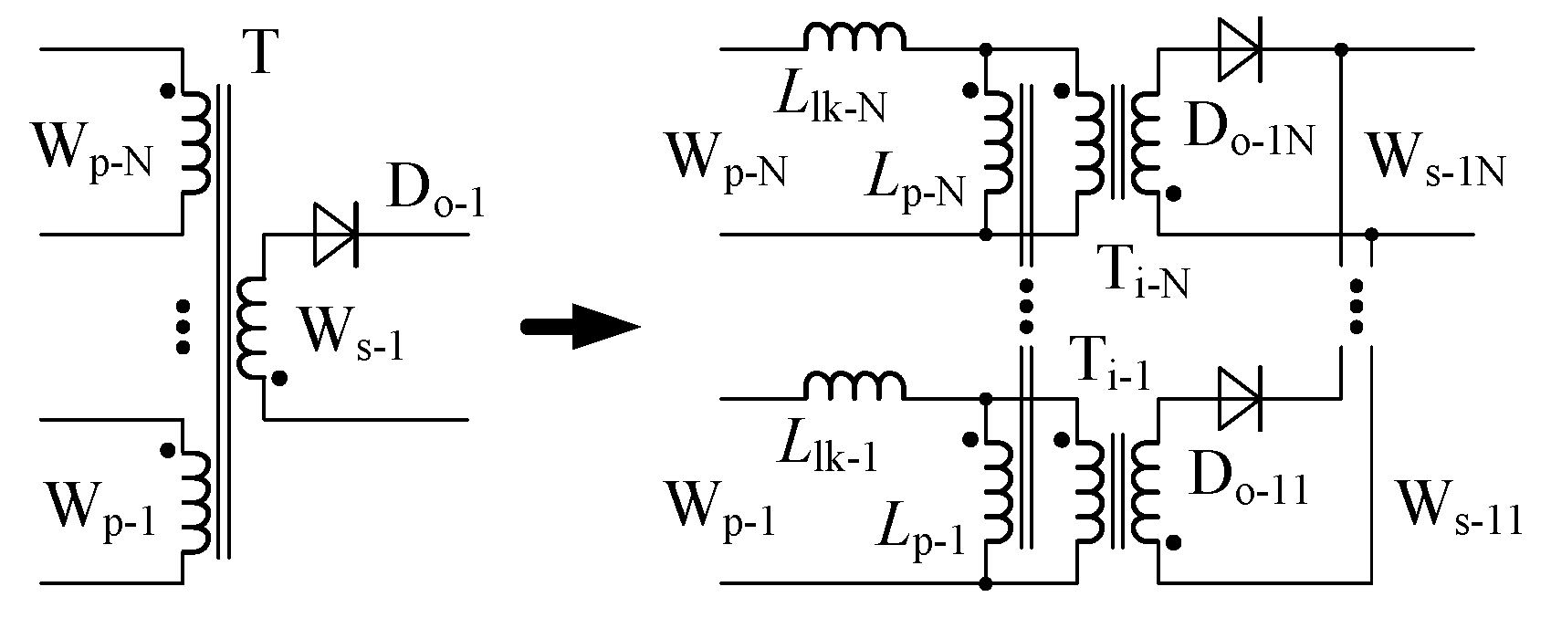
Figure 4.
Main voltage and current waveforms in each period.
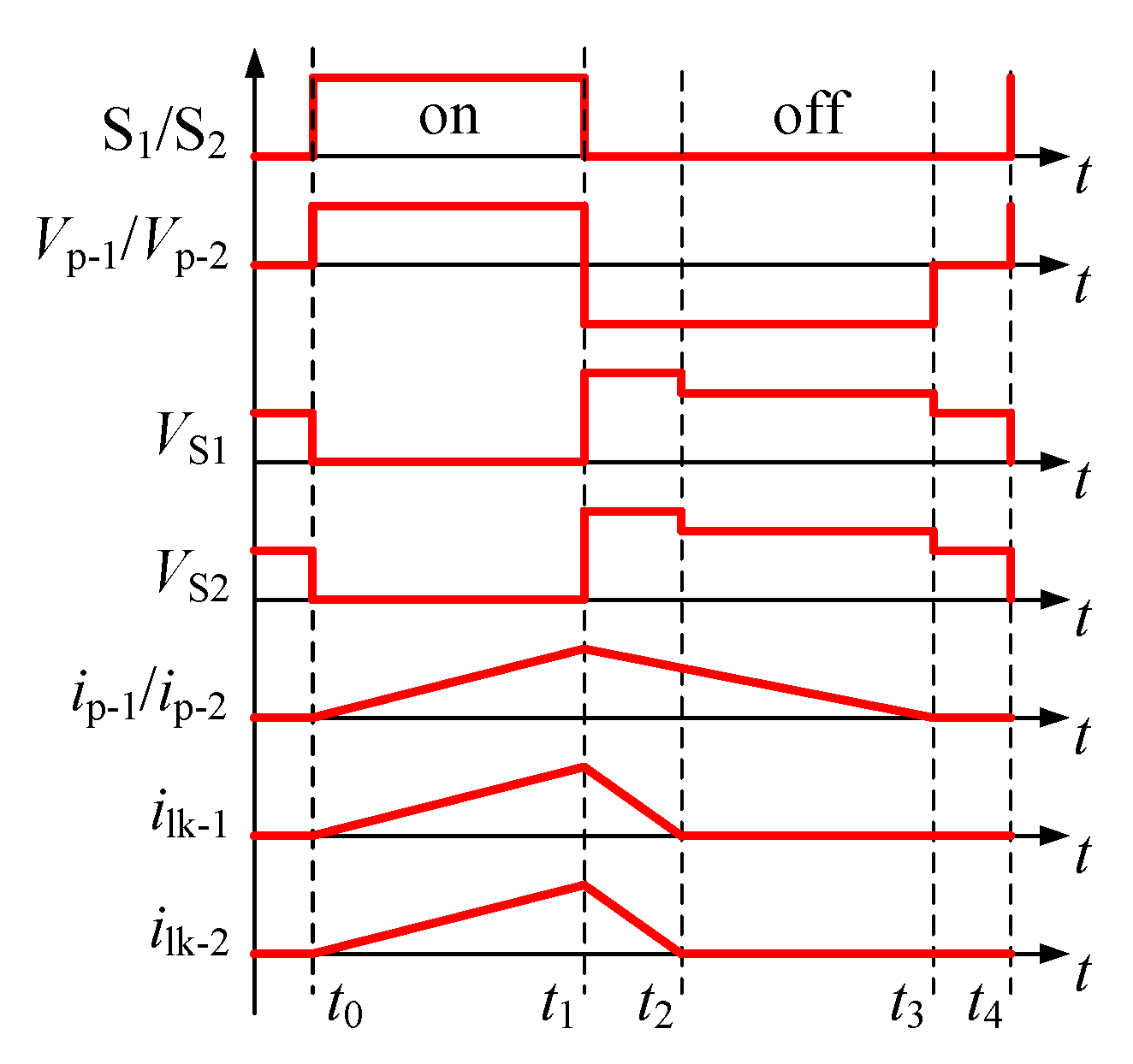
Figure 5.
Equivalent circuit in each stage. (a) Stage 1. (b) Stage 2. (c) Stage 3. (d) Stage 4.
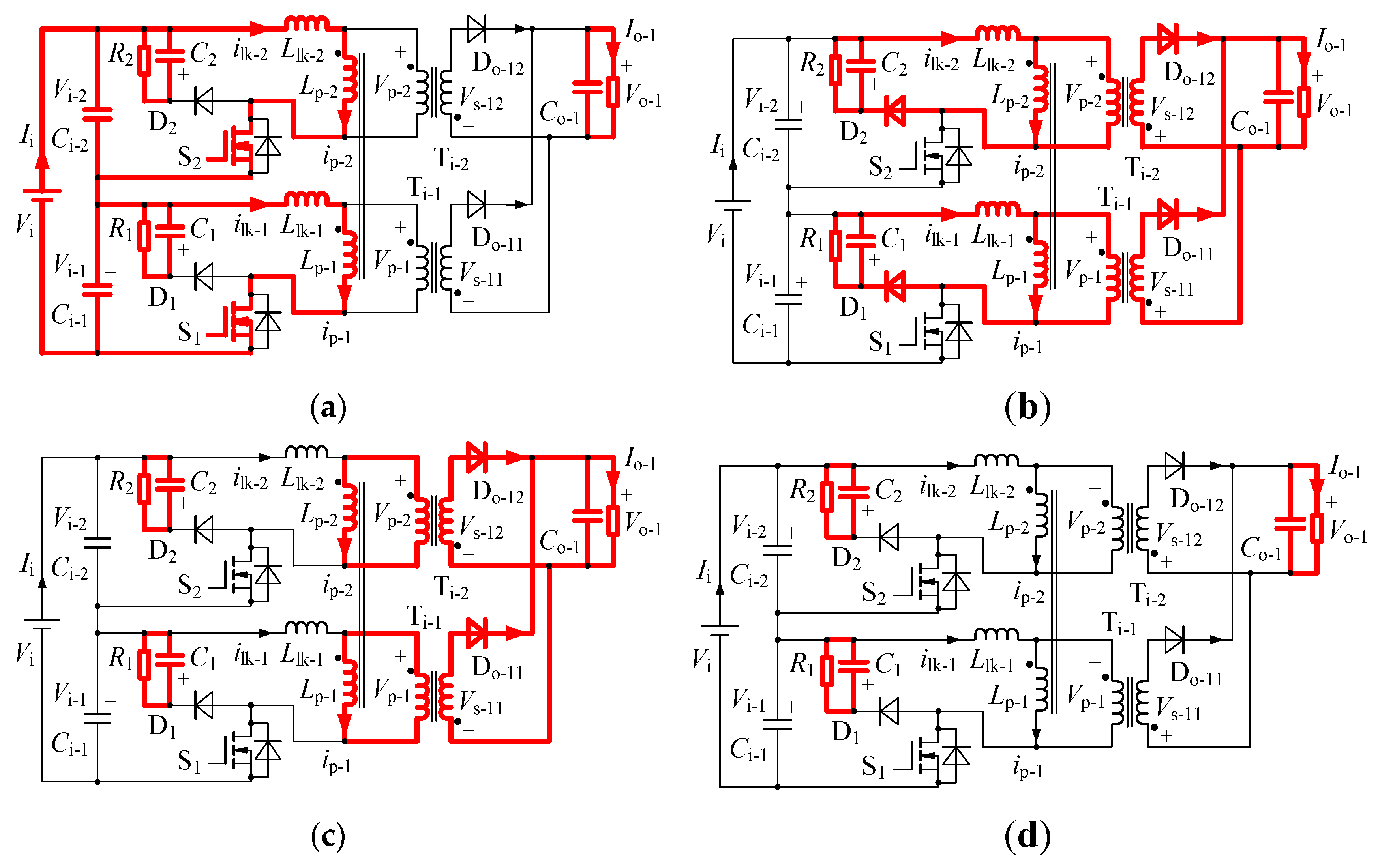
Figure 6.
Simplified equivalent circuit of the ISTI flyback converter in stage 2 (Vs-11=Vs-12= -Vo-1 and Vp-1=Vp-2= -Np-1Vo-1/Ns-1).
Figure 6.
Simplified equivalent circuit of the ISTI flyback converter in stage 2 (Vs-11=Vs-12= -Vo-1 and Vp-1=Vp-2= -Np-1Vo-1/Ns-1).
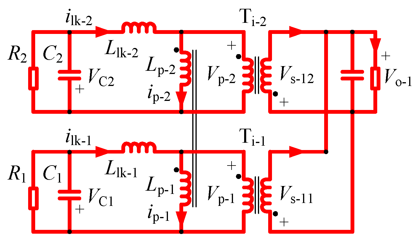
Figure 7.
Experimental prototype of the ISTI flyback converter.
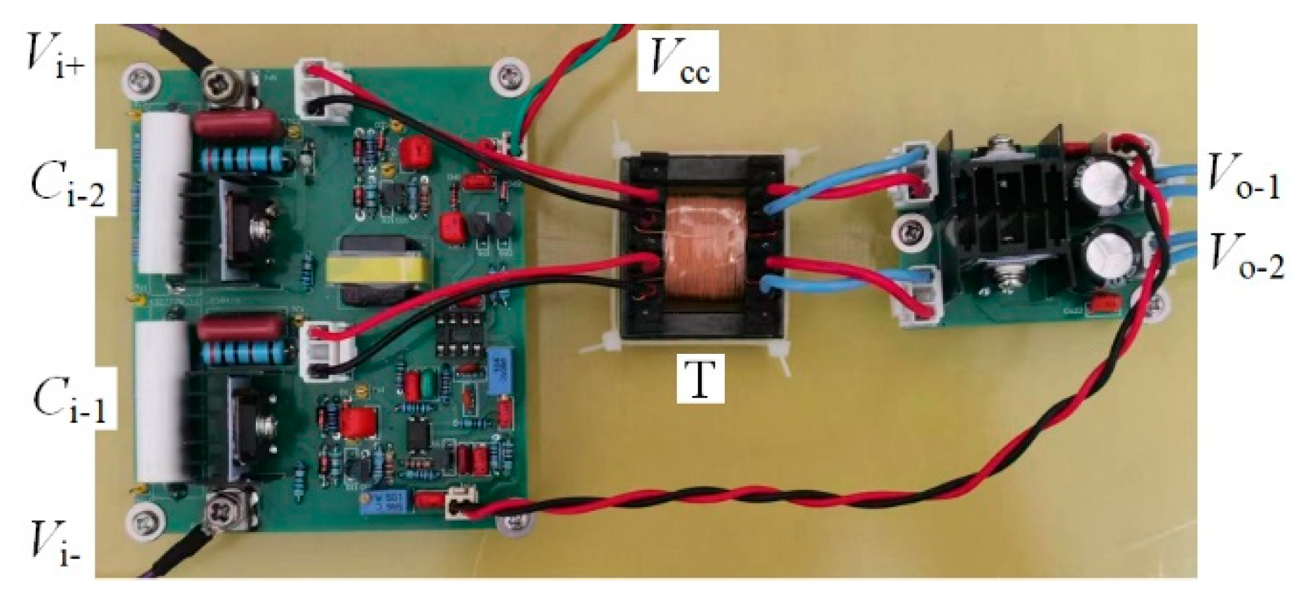
Figure 8.
Cross sections of the flyback integrated-transformer. (a) The illustration of T1. (b) The illustration of T2. (c) The illustration of T3.
Figure 8.
Cross sections of the flyback integrated-transformer. (a) The illustration of T1. (b) The illustration of T2. (c) The illustration of T3.
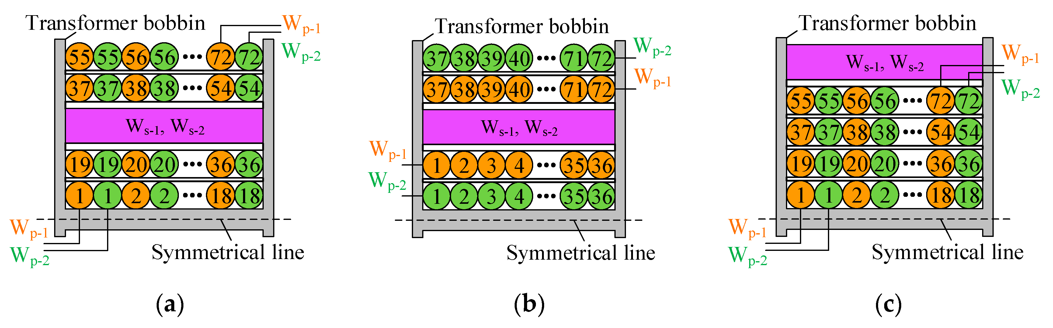
Figure 9.
Main waveforms of the prototype when T1 is used. (a) Voltage and current of S1. (b) Voltage and current of S2. (c) Input voltages (Vi-1, Vi-2). (d) Voltages of C1 and C2.
Figure 9.
Main waveforms of the prototype when T1 is used. (a) Voltage and current of S1. (b) Voltage and current of S2. (c) Input voltages (Vi-1, Vi-2). (d) Voltages of C1 and C2.
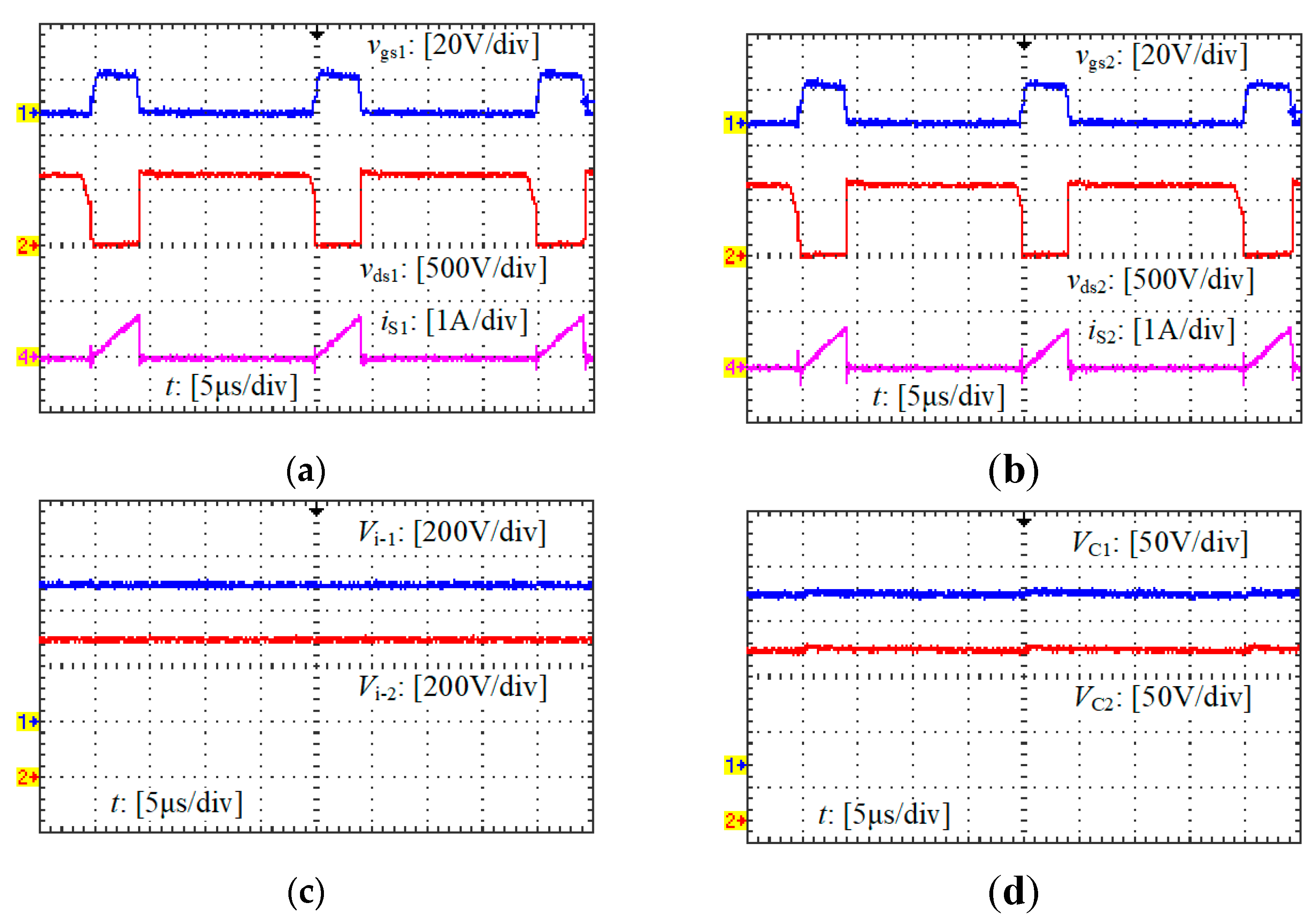
Figure 10.
Main waveforms of the prototype when T2 is used. (a) Voltage and current of S1. (b) Voltage and current of S2. (c) Input voltages (Vi-1, Vi-2). (d) Voltages of C1 and C2.
Figure 10.
Main waveforms of the prototype when T2 is used. (a) Voltage and current of S1. (b) Voltage and current of S2. (c) Input voltages (Vi-1, Vi-2). (d) Voltages of C1 and C2.
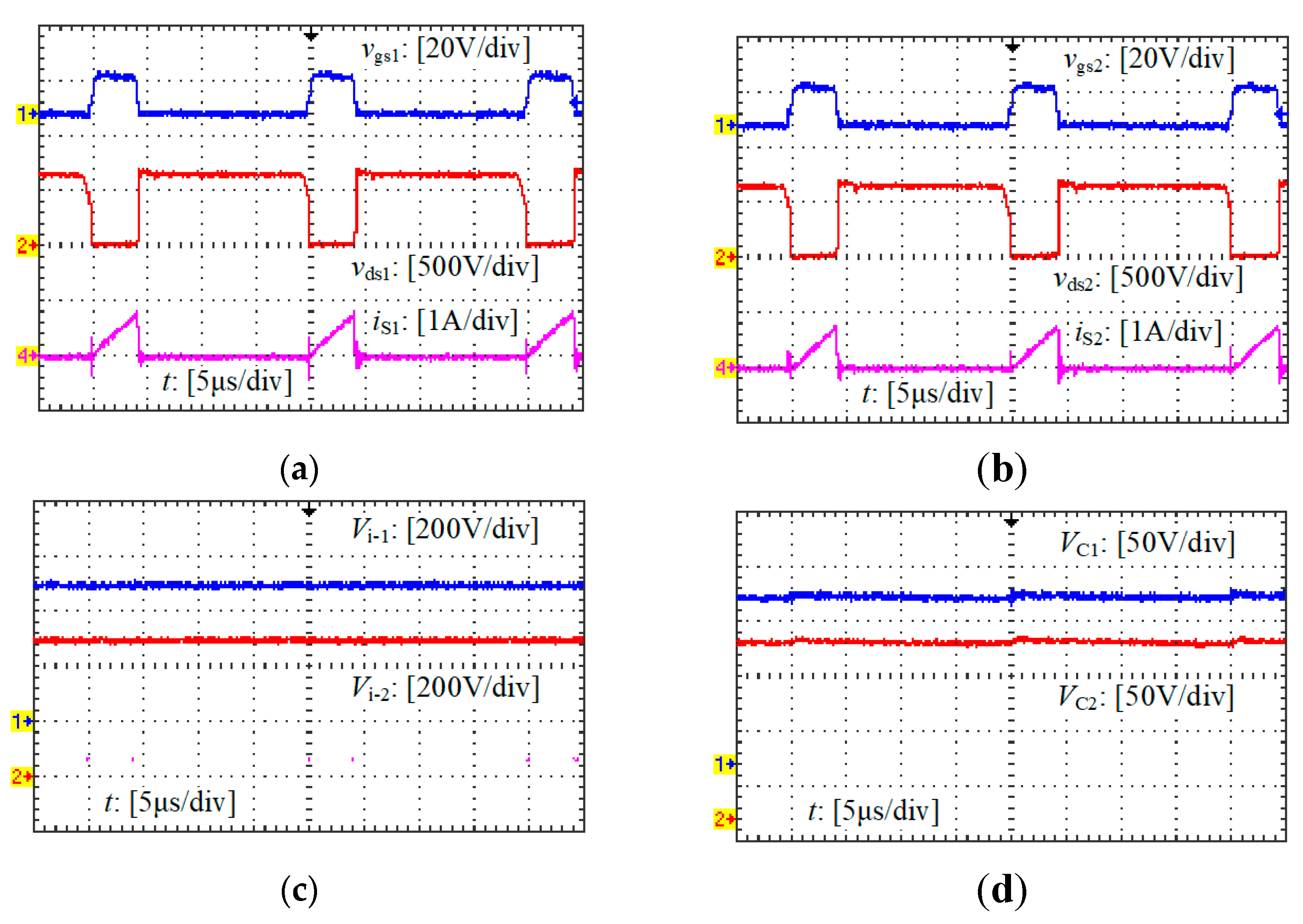
Figure 11.
Main waveforms of the prototype when T3 is used. (a) Voltage and current of S1. (b) Voltage and current of S2. (c) Input voltages (Vi-1, Vi-2). (d) Voltages of C1 and C2.
Figure 11.
Main waveforms of the prototype when T3 is used. (a) Voltage and current of S1. (b) Voltage and current of S2. (c) Input voltages (Vi-1, Vi-2). (d) Voltages of C1 and C2.
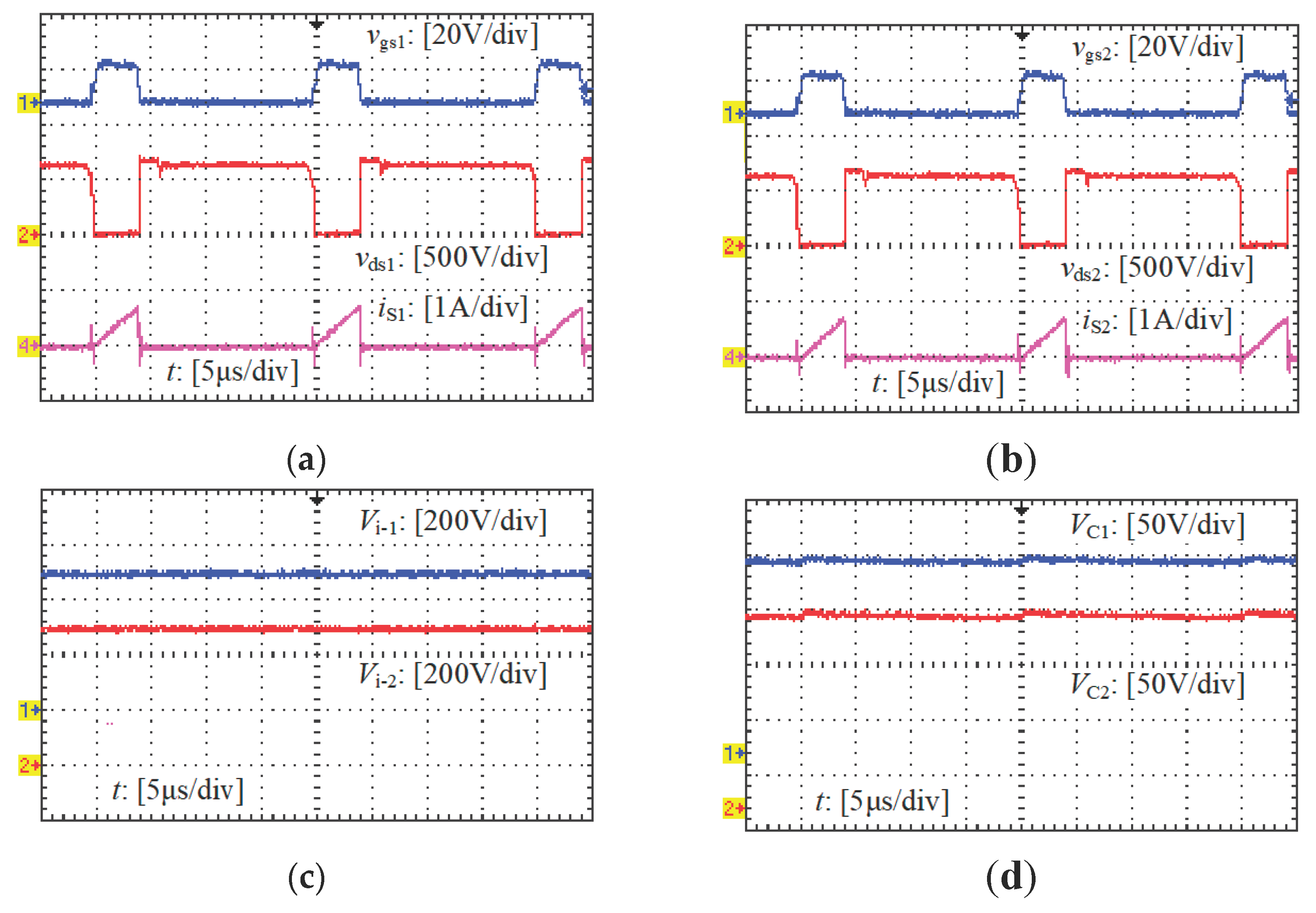

Table 1.
Components and parameters of the prototype.
| Components or parameters | Features or values |
|---|---|
| Vi | 1000 V (N=2) |
| Vo-1, Vo-2 | 24V (Vo-1=Vo-2, n=2) |
| Io-1, Io-2 | 1.5 A, 1 A |
| Ci-1, Ci-2 | 1200 V/0.1 μF (Ci-1=Ci-2) |
| S1, S2 | 2SK1271 (T=20 μs) |
| Do-1, Do-2 | MUR1560 |
| Co-1, Co-2 | 50 V/1000 μF (Co-1=Co-2) |
| R1, R2 | 15 kΩ (R1=R2) |
| C1, C2 | 630 V/0.1 μF (C1=C2) |
| D1, D2 | BYV26G |
Table 2.
Common features of the integrated-transformers.
| Types or parameters | Features or values |
|---|---|
| Magnetic core | EI 40 (Ferroxcube) |
| Np-1, Np-2 | 72 (Np-1=Np-2) |
| Ns-1, Ns-2 | 14 (Ns-1=Ns-2) |
| Lp-1, Lp-2 | 1.36 mH (Lp-1=Lp-2) |
| Layer number (Wp-1, Wp-2) | 4 |
Table 3.
Measuring results of the integrated-transformer.
| T | T1 | T2 | T3 |
|---|---|---|---|
| k12 | 0.998999 | 0.997627 | 0.999130 |
| Llk-1 | 13 μH | 11 μH | 36 μH |
| Llk-2 | 13 μH | 18 μH | 35 μH |
Table 4.
Main measuring results.
| T | T1 | T2 | T3 |
|---|---|---|---|
| VC1 | 155 V | 152 V | 175 V |
| VC2 | 155 V | 161 V | 175 V |
| η | 87.12% | 87.01% | 83.78% |
Disclaimer/Publisher’s Note: The statements, opinions and data contained in all publications are solely those of the individual author(s) and contributor(s) and not of MDPI and/or the editor(s). MDPI and/or the editor(s) disclaim responsibility for any injury to people or property resulting from any ideas, methods, instructions or products referred to in the content. |
© 2025 by the authors. Licensee MDPI, Basel, Switzerland. This article is an open access article distributed under the terms and conditions of the Creative Commons Attribution (CC BY) license (http://creativecommons.org/licenses/by/4.0/).
Copyright: This open access article is published under a Creative Commons CC BY 4.0 license, which permit the free download, distribution, and reuse, provided that the author and preprint are cited in any reuse.


