
Submitted:
27 November 2025
Posted:
28 November 2025
You are already at the latest version
Abstract
With the rapid growth of secure communication and data integrity needs in embedded and networked systems, there is a growing demand for cryptographic solutions that are not only secure but also energy- and area-efficient. While software-based SHA-3 implementations offer flexibility, they often fall short in meeting the tight performance and power budgets of modern resource-constrained environments. This paper presents a hardware-accelerated SHA-3 implementation optimised for the Xilinx Artix-7 FPGA. The proposed architecture features a fully pipelined Keccak-f[1600] core and leverages techniques such as partial loop unrolling, clock gating, and pipeline balancing to improve efficiency. Designed in VHDL and synthesised using Vivado 2024.2.2, the accelerator achieves a throughput of 1.35 Gbps at 210 MHz with a total power consumption of just 0.94 W—resulting in an energy efficiency of 1.44 Gbps/W. The design is validated against NIST SHA-3 test vectors and demonstrates a strong balance between speed, low power, and hardware utilisation. These characteristics make it well-suited for deployment in secure embedded applications, such as IoT devices, edge nodes, and real-time authentication systems.
Keywords:
SHA-3
; Keccak-f[1600]
; FPGA
; hardware accelerator
; Artix-7
; low-power design
; energyefficient computing
; embedded systems
; cryptographic hardware
1. Introduction
The proliferation of digital systems across domains such as finance, industrial automation, cloud computing, and the Internet of Things (IoT) has heightened the importance of robust data integrity and authentication mechanisms. In these interconnected environments, secure communication must go beyond confidentiality to include reliable detection of data tampering or unauthorised modifications. [1,2] Cryptographic hash functions offer a foundational solution by converting inputs of arbitrary length into fixed-size digests that are highly sensitive to any change [3,4].
In 2015[5], the National Institute of Standards and Technology (NIST) standardised the Secure Hash Algorithm 3 (SHA-3), representing a significant advancement in cryptographic hashing. Built on the Keccak sponge construction, SHA-3 provides strong resistance to collision and preimage attacks, and supports variable output lengths suited for diverse application needs [6,7,8,9]. However, its Keccak-f [1600] core, comprising 24 rounds of complex transformations, makes software implementations unsuitable for latency- - and energy-sensitive embedded systems. [6,8]. Consequently, hardware acceleration—particularly via Field-Programmable Gate Arrays (FPGAs)—has emerged as a viable alternative, thanks to FPGAs’ parallelism, reconfigurability, and deterministic timing behaviour [11,12].
Recent studies continue to confirm the effectiveness of SHA-3 implementations on low-cost, energy-efficient FPGA platforms such as Artix-7. For example, Korona et al. demonstrated that hardware-accelerated hash functions, including SHA-3, can be integrated into network traffic probes to improve throughput and reduce energy consumption without significantly increasing area [11]. Similarly, Leonardi et al. explored hardware-software co-design for cryptographic tasks in Industrial IoT, showing that SHA-3 accelerators can operate within strict energy and latency limits while maintaining compatibility with real-time embedded systems [12].
1.1. Motivation and Research Gap
Existing SHA-3 FPGA accelerators targeting high-end devices (e.g., Xilinx Virtex-7 or Kintex-7) have achieved throughputs exceeding 2.5 Gbps through deep pipelining and extensive loop unrolling. [7,15]. Yet these gains come with increased power consumption (exceeding 3 W) and large resource footprints, limiting their suitability for embedded or battery-powered systems [15]. Some system-on-chip (SoC) approaches on platforms such as the Zynq-7000 have improved energy efficiency, but at the cost of increased design complexity [11,17]. While mid-range devices such as Artix-7 are widely used in cost- - and power-constrained environments, relatively few SHA-3 implementations exploit their architectural advantages, and many designs still prioritise raw throughput or minimal area over energy-per-bit efficiency [7,18].
Additional research highlights the growing relevance of SHA-3 accelerators in edge and IoT contexts. For instance, Baird et al. examined the energy implications of SHA-3 (including KangarooTwelve) on constrained devices, concluding that modern FPGA-based implementations offer strong cryptographic performance while keeping energy costs manageable [12]. In parallel, Potestad-Ordóñez et al. proposed hardware fault protection techniques for cryptographic FPGA cores, reinforcing the viability of SHA-3 in mission-critical or harsh operating conditions [18]. Together, these contributions indicate SHA-3's growing role in secure, high-performance, and energy-aware embedded systems.
To address this gap, we propose an energy-aware SHA-3 accelerator optimised for the Artix-7 FPGA, incorporating selective loop unrolling, balanced pipelining, and dynamic clock gating to achieve a practical balance between throughput, power, and resource use.
1.2. Contributions
This work introduces a power-aware SHA-3 hardware accelerator tuned for the Xilinx Artix-7 FPGA. Unlike prior designs that primarily focus on either maximising performance or minimising resource consumption, our approach delivers a balanced solution tailored for embedded systems with limited energy and area budgets. The main contributions include:
- A pipelined Keccak-f[1600] core with balanced stage segmentation, loop unrolling, and logic reuse to enable high throughput with low resource overhead.
- An energy-aware design using dynamic clock gating to reduce idle switching activity while supporting high-speed operation.
- Demonstrated energy efficiency of 1.44 Gbps/W, surpassing many recent FPGA-based SHA-3 implementations.
- Full validation using NIST test vectors for functional correctness, followed by post-synthesis performance verification.
The proposed design features a compact footprint and is suitable for applications ranging from embedded systems and VPN modules to network authentication devices and IoT edge nodes.
The remainder of this paper is structured as follows: Section 2 explores prior contributions and situates our work within the current landscape. Section 3 explains the design methodology, guiding the reader through each development phase. Section 4 outlines the architecture and presents our implementation results. Section 5 offers a thorough discussion, interpreting key findings and implications. Section 6 summarises our conclusions, while Section 7 reflects on possible future directions for extending this research. This structure aims to provide a straightforward, engaging narrative that balances technical depth with accessibility for a broad audience.
2. Related Work
Moreover, the acceleration of cryptographic systems has made a significant progress itself, due to the ever-growing need for secure, low-latency data processing in embedded and power-constrained systems. Of these, Field-Programmable Gate Arrays (FPGAs) have become a popular option, as their parallelism, configurability, and deterministic execution properties make them well-suited for implementing computationally intensive hash functions like SHA-3 [11,16,20].
Almost all early FPGA-based SHA-3 accelerators were designed for performance, and generally use high-end devices such as Xilinx Virtex-7 and Kintex-7. For instance, Ioannou et al. CSN published the first fully unrolled, deeply pipelined SHA-3 architecture on the Virtex-7, offering very high throughput [10], but at a significant power cost. Similarly, Sideris et al. presented A lightweight implementation of the Keccak family onto an FPGA in [6], which aimed at minimising energy for a given throughput. Authors [13] Proposed a high-speed Keccak design for the Kintex-7 series, aiming for raw processing speed rather than energy efficiency or area minimisation.
Although these strategies exploit deep pipelining and parallelism, their applicability can be reduced in battery-powered or embedded systems due to their high energy footprints.
Later works made a transition to more balanced architectures with consideration of power and area constraints. An example of a pipelined SHA-3 core implemented on Spartan-6 FPGAs is the one proposed by Kahri [6]. Whereby logic reuse and partial unrolling were used to achieve a high resource efficiency. Later, Dolmeta et al. [11,16] have generalised this by embedding a Keccak engine in a RISC-V-based SoC to achieve medium throughput with affordable energy costs of a hybrid processor-accelerator system.
Researchers also investigated methods to enhance scalability and parallelisation. Ren et al. Lastly, a multi-core SHA-3 with adaptive clocking supports parallel hash computations [20], but adaptively reduces power when overall power consumption is high. In parallel, Xiong et al. There exist several folded SHA-3 designs that keep hardware resource usage low at the expense of functional correctness, thereby catering to low-resource designs for low-power applications such as IoT nodes [21].
Recent designs have advanced energy efficiency in FPGA-based SHA-3 accelerators by adopting folding, time-sharing, and integration-centric techniques tailored for constrained platforms. For example, Leonardi et al. [11] demonstrated a hybrid hardware-software co-design for cryptographic functions targeting industrial IoT, emphasising flexible system partitioning and secure data handling under power and cost constraints. Baird et al. [14] provided an energy-aware analysis comparing SHA-3 (KangarooTwelve) and SHA-256 on low-end devices, reinforcing the trade-offs between throughput and battery longevity in portable systems. Meanwhile, Magyari and Chen [22] reviewed the application of FPGA-based cryptographic modules in IoT networks, underscoring SHA-3’s role in scalable, real-time hardware pipelines. Further strengthening this direction, Potestad-Ordóñez et al. [19] proposed fault-resistant FPGA-based SHA-3 modules with ADC-assisted detection, thereby enhancing cryptographic resilience against physical attacks. Stoyanov et al. [23] introduced a heterogeneous security architecture for embedded education systems, integrating cryptographic modules into FPGA platforms for prototyping and training. Finally, Korona et al. [24] benchmarked SHA family functions for real-time network traffic probes, highlighting SHA-3’s suitability for high-throughput, low-latency packet processing.
Reliability focus has also been increasing beyond performance and efficiency. Torres-Alvarado et al. In [25] a fault-tolerant SHA-3 implementation is proposed that detects errors using Hamming encoding to increase robustness against hardware faults. Additionally, Rogawski et al. Then, in [16] SHA-3 was also specified to support configurable SHAKE functions, which are better suited to modern cryptographic protocols.
In more recent work, researchers have begun integrating SHA-3 cores into larger security systems. In accordance with the works of Sideris and Dasygenis [26] and Akiya et al. Such applications [27] demonstrate how Keccak accelerators can be integrated into a secure boot chain, a firewall, and a real-time packet inspection unit, respectively, and highlight the use of SHA-3 in layered security architectures.
Although FPGA families are mature enough for acceleration, mid-range families like the Xilinx Artix-7 remain underexplored in the SHA-3 acceleration literature. The inflexion points of this class of devices, specifically their sweet spot between power, price and performance, make this architecture great for embedded use cases. Nevertheless, there are only a few works [4,15,18]. Focusing on the customisation of SHA-3 designs suitable for utilising all architectural aspects of the Artix-7 family.
For instance, Baird et al. [12] Evaluated SHA-3 hashing on constrained IoT devices, revealing that energy costs can be significantly reduced without compromising throughput by carefully tuning architectural choices. Similarly, Leonardi et al. [11] Demonstrated the integration of SHA-3 accelerators within low-power industrial systems, showing that Artix-7 class FPGAs can deliver secure performance with minimal resource overhead, making them highly suitable for embedded and edge applications.
In this work, we fill this gap and propose a SHA-3 accelerator for real applications that is energy-efficient and specifically designed for Artix-7 FPGAs. The design utilises selective unrolling, pipelining for throughput, and dynamic clock gating to achieve near-optimal power and throughput while maintaining a small logic size.
In summary, while the body of work on high-performance SHA-3 implementations is substantial, the practical deployment of such solutions in resource-limited systems remains an open challenge. This study contributes by offering a power-aware, performance-balanced SHA-3 architecture that is both feasible and efficient for secure embedded applications.
3. Methodology and Design Approach
The work presented presents a structured design methodology for realising a high-level energy-efficient SHA-3 accelerator on a resource-constrained FPGA (Xilinx Artix-7) while retaining algorithmic characteristics, hardware efficiency, and architectural scalability. The approach combines an in-depth analysis of the cryptographic function with a pragmatic digital design approach, balancing adherence to the SHA-3 standard with performance and power optimisation in an embedded environment.
In Figure 1, we describe the design flow via five stages in the methodology:
- Functional Analyst on Keccak-f [1600]: This stage analyses the 24-round permutation core that is the computational engine behind SHA-3. And a well-defined structure will help you to gain efficient hardware mapping.
- Architectural Modelling: A modular architecture is designed where each block, e.g. input formatter, Keccak core and output logic, is handled as an independent, reusable component. Such a design not only permits the trivial scaling of the number of attendees involved in computation, but also simplifies the embedding of use of such a protocol within a larger cryptographic system.
- Design Optimisation: Loop unrolling techniques (even partial loop unrolling), balanced segmentation of pipeline stages, and resource sharing (where tailoring is done to meet individual design metrics) are performed to improve throughput and to mitigate the uncertainty of switching activity and to improve energy efficiency.
- Architecture in VHDL: The architecture for the design is described in VHDL and implemented using the Xilinx Vivado 2024.2.2 toolchain. During synthesis and place-and-route, great care is taken to adhere to timing constraints, manage clocks, and allocate resources.
- Validation and Testing: Official NIST SHA-3 test vectors are used to validate functional correctness. Timing closure and performance metrics are verified to ensure real-world deployability.
Such a step-by-step methodology facilitates the accurate manipulation of design parameters, enabling fine-grained tuning of the trade-off between throughput, power consumption, and logic utilisation. For embedded and real-time systems, performance predictability and tight energy budgets are key design constraints; hence, this kind of optimisation is essential.
This process aligns with methodologies observed in recent energy-conscious SHA-3 accelerator designs, such as those in [12,24], where modular system architectures and application-specific optimisations enabled practical deployments on resource-constrained and mid-range FPGA platforms like the Artix-7.
In addition, the architecture can be easily extended or integrated with other systems due to its modular, reusable nature. Examples include the ability to design support for different cryptographic standards or to embed within larger security subsystems (e.g., VPN routers, IoT gateways, and intrusion detection modules).
This approach provides a scalable SHA-3 accelerator that leverages algorithm-level insights and hardware-specific optimisations, making it applicable to both power-aware and security-sensitive embedded systems.
Furthermore, recent work by Potestad-Ordóñez et al. [18] demonstrates the effectiveness of low-power strategies—such as fault detection through analogue monitoring—within FPGA-based cryptographic designs. These methods complement our approach, particularly in contexts where predictable power behaviour and secure, real-time operation are essential.
Complementing the structured methodology, the design process benefits significantly from its modular and reusable framework. Each architectural block—such as the input formatter, Keccak core, and post-processing unit—is designed to function independently, making the system easier to validate, maintain, and adapt. This modularity not only accelerates the development cycle but also simplifies integration into broader cryptographic systems, where subsystems often evolve or require updates to meet new security demands.
A similar modular approach was discussed in [22], where the SHA-3 implementation was designed with flexible core modules, allowing seamless upgrades to SHAKE or cSHAKE variants without requiring a complete datapath redesign. This highlights the growing importance of scalable, adaptable cryptographic cores in modern FPGA-based systems.
Moreover, using a hardware description language such as VHDL offers long-term flexibility, enabling the design to be ported across different FPGA families or toolchains with minimal modification. Such portability is particularly valuable in embedded systems, where hardware longevity and adaptability are critical. As security requirements shift and new standards emerge, this architecture is well-positioned to evolve, either by adding support for newer hash functions or by embedding the accelerator into more comprehensive security solutions.
For instance, Potestad-Ordóñez et al. [18] Propose a compact and energy-aware SHA-3 architecture for FPGA systems, emphasising fault detection and low resource usage. Their implementation demonstrates that secure, high-throughput hashing is feasible even on constrained devices such as Artix-7, supporting the suitability of such platforms for modern IoT environments.
Together, these qualities reinforce the practical value of the proposed approach—providing a solid foundation not only for immediate deployment but also for future-proof development in energy-conscious and security-sensitive environments.
Beyond technical efficiency, this design approach supports real-world deployment by addressing the practical limitations faced in embedded systems—such as limited power budgets and hardware constraints. By focusing on modularity and portability, the accelerator can easily be tailored to evolving security standards and adapted for diverse applications, from intelligent IoT nodes to secure communication modules. This ensures that the system is not only performant today but remains relevant and scalable in the years ahead.
The accelerator needs to influence each stage of the design workflow to effectively shape the performance attributes and energy profile of this final product. Complete adherence to the SHA-3 standard guarantees that the implementation is secure against initial algorithmic analysis. This is the foundation for that kind of security. The subsequent stage is architectural modelling and optimisation, in which power and data throughput are minimised and larger constraints, such as those imposed by a particular FPGA type, are considered.
Finally, implementation and validation verify if the design meets the functional and timing requirements and thus is executable in the embedded real-time environment.
3.1. Proposed Design Methodology
The design process began with a functional analysis of the Keccak-f [1600] permutation, the underlying component of the SHA-3 cryptographic standard. The Keccak family, for example, has a 1600-bit internal state arranged as five columns of five rows of 64-bit lanes, as depicted below. The algorithm uses five distinct transformation steps (Theta (θ), Rho (ρ), Pi (π), Chi (χ), and Iota (ι)), each of which is applied 24 rounds to achieve essential cryptographic characteristics such as diffusion, non-linearity and round-variable properties [6]. Combined, these features bolster the algorithm against familiar attacks, especially collision and preimage attacks [3,8].
After decomposing the design according to the steps of this algorithm, it was specified in VHDL using a fully pipelined architecture, where each pipeline stage corresponds to one complete round of the Keccak-f[1600] permutation. This technique enables the processing of many message blocks in parallel, helping reduce end-to-end delay and improve the throughput of the incoming message stream. Deep pipelining also has an established track record in high-speed crypto hardware design (continuous processing of input blocks while maintaining correctness and integrity per round transformations) [12,16].
This design approach aligns with the approach of Magyari and Chen [22], who employed pipeline reuse and dynamic logic simplification to maintain throughput while reducing the number of active slices per cycle—an effective strategy in energy-aware cryptographic accelerators.
3.2. System-Level Architecture Overview
To implement the SHA-3 accelerator, three closely coupled hardware modules are designed, one for each stage of the hashing operation. Collectively, those components create a straight-through data path that provides high throughput, stable timing, and full compliance with the SHA-3-256 specification.
3.2.1. Pre-Processing Unit
This module preps input data according to the SHA-3 specs. First, it handles message padding/segmentation, dividing the incoming data stream into 1088-bit blocks of fixed size, as is required of the SHA3-256 variant. This keeps each message aligned and validated with the core hashing engine, which maintains data integrity as it moves through the input unit.
3.2.2. Keccak Processing Core
The architecture's core consists of the Keccak core, which operates in a 24-stage pipelined manner. The combiner logic and intermediate registers for each point stage carry out one complete round of a Keccak-f [1600] round. This allows parallel processing of message blocks, increasing throughput and reducing latency. This pipelined SHA-3 implementation has previously been implemented in high-performance [7,16], and in the mid-range of FPGAs [10,12], so it is clear that it is both scalable and effective.
3.2.3. Post-Processing Unit
Once the sponge function completes, the post-processing unit receives the final hash output and shrinks it to 256 bits. The logic here checks and combines the final digest to verify and synchronise it, then forms and aligns the production for downstream use.
The three modules are synchronised through internal bus interfaces and are clocked in the same domain. A unified timing model enables predictable latencies and supports predictable timing closure—key aspects for integration into real-time and networked systems [9,27].
This interface cohesion reflects the approach in [18], where FPGA-based cryptographic modules were integrated with ADC-driven fault detection, maintaining system reliability with minimal latency overhead during real-time operations.
Figure 2 illustrates the overall organisation of the SHA-3 accelerator, providing more details on its main components and their interconnections within the system architecture. It shows the path of data from the first input through processing and padding to the pipelined Keccak core's output and the final hash. This separation is likewise declunky, yet it continues to deliver high performance and low power, both characteristics necessary for embedded and real-time applications.
3.2.4. Optimisation Techniques for High Performance and Efficiency
To achieve a higher throughput and energy efficiency from the SHA-3 accelerator, including the following architectural enhancements:
- Resource Sharing: To reduce LUT usage with no performance overhead, logic reuse techniques were implemented.
- Manual Floor planning: Vivado 2024.2.2 was used to manually optimise timing paths to enhance both placement and routing, as well as provide overall timing [26].
Our architectural optimisations align with the methodologies discussed by Leonardi et al. [11] and Baird et al. [12], where power-aware layout strategies and hardware-software co-design were leveraged to achieve secure and efficient hashing in embedded systems. These efforts underscore the importance of FPGA-level configurability and pipeline balance in meeting real-time throughput targets without exceeding energy constraints.
Such optimisation strategies are commonly employed in energy-aware FPGA design, particularly when tight trade-offs exist among power, area, and speed.
It is important to note that the implementation always stayed, at most, within 20% of the available BRAM on the Artix-7. This proves that the design is scalable and provides a scope to incorporate additional security modules or communication interfaces without stressing on-chip memory resources.
In Figure 3, we show the internal pipeline of the Keccak-f [1600] core to illustrate how efficiently the design can execute the data flow. We represent the five transformation stages: Theta, Rho, Pi, Chi, and Iota, working in harmony with the round constant generator and clock-gating control block to enable high-performance levels with low energy consumption.
Together, these optimisation strategies form the foundation of the accelerator's performance profile, which is further analysed in the following section.
3.2.5. Synthesis and Verification
The functional correctness of the proposed SHA-3 accelerator was ensured using the Vivado Simulator and matched the official NIST SHA-3 test vectors [3,6]. The VHDL was synthesised for the Xilinx Artix-7 XC7A100T-CSG324 FPGA, with timing analysis yielding zero negative slack; all timing constraints were met.
An Integrated Logic Analyser (ILA) core was instantiated to perform real-time debugging and signal tracing. The hardware behaviour was verified by validating message lengths from 0 bits to 1 MB and various clock configurations, with consistent operation and in agreement with the previously detailed SHA-3 hardware validation methods [9,17].
3.2.6. Performance Metrics
To evaluate the operational throughput and efficiency of the proposed design, the SHA-3 accelerator was implemented and validated on the Xilinx Artix-7 platform. The maximum operating frequency, data throughput, power, and hardware utilisation are essential key performance indicators summarised in Table 1.
Key performance indicators, including a peak frequency of 210 MHz, a throughput of 1.35 Gbps, and a total power consumption of 0.94 W, yield an energy efficiency of 1.44 Gbps/W. This compares favourably with recent studies, such as those by Baird et al. [12], where energy efficiency for SHA-3 hashing in IoT devices ranged from 0.9 to 1.2 Gbps/W across different configurations. Likewise, Leonardi et al. [11] Explored hardware–software co-design for cryptographic accelerators and emphasised the importance of efficient logic partitioning to achieve low latency and balanced energy profiles in industrial IoT systems. These results confirm the relevance of our optimisations, which accomplish a similar level of performance tuning and resource awareness.
This assessment validates the design's effectiveness in maintaining high energy efficiency, performance, and resource efficiency simultaneously, which is crucial, especially for embedded and networked systems.
Table 1 shows that the peak operating frequency for the accelerator is 210.43 MHz, and a sustained throughput of 1.35 Gbps is achieved when the pipeline is fully utilised. At a total power of 0.94 W, the design achieves a performance-per-watt efficiency of 1.44 Gbps/W, representing a significant energy-efficiency advance over previously reported mid-range FPGA realisations of SHA-3 [10,16,27].
The results show that the pipelined architecture described in this paper achieves a good trade-off between speed, power, and area, indicating its potential for online energy-efficient cryptographic applications.
3.2.7. Comparative Analysis with Existing Work
To appropriately assess the performance of the proposed SHA-3 accelerator, Table a compares various SHA-3 hardware implementations on an FPGA. The following table summarises key parameters, including throughput, power, and energy efficiency, for recent designs reported in the literature. We aim not just to showcase raw performance but to demonstrate how well each solution strikes the ideal balance of speed and power—essential for many applications in which energy consumption is a key factor.
Recent work, such as Leonardi et al. [11] has demonstrated the potential of integrated hardware–software SHA-3 accelerators within industrial IoT environments, focusing on real-time performance and energy control, similarly, Baird et al. [12] evaluated SHA-3 variants like KangarooTwelve under constrained conditions, reporting energy efficiencies ranging from 0.9 to 1.2 Gbps/W, depending on workload and core configuration. Compared to these, our implementation achieves a balanced throughput of 1.35 Gbps at 0.94 W (1.44 Gbps/W), showing competitive efficiency with lower area overhead. At the same time, some designs emphasise raw throughput, such as Korona et al. [24] our strategy prioritises consistent energy usage and timing determinism, making it better suited to embedded or edge deployments.
These results are summarised in Table 2, which shows that the energy efficiency of the SHA-3 accelerators proposed here is competitive with that of other works. Although raw throughput much higher than that delivered by previous designs is possible, this comes typically at a high cost, specifically, much higher power consumption and the need for larger FPGA platforms. Our results are consistent with the most efficient mid-range accelerators, but with a smaller footprint and lower cost, making it more attractive for production use.
This work, however, presents a more balanced solution, providing a good trade-off between performance and power consumption using an affordable cost Artix-7 device. All of this makes it a suitable candidate for real-world applications, where efficient cryptographic processing is necessary in constrained environments such as IoT devices and embedded security systems.
4. System Architecture and Implementation Results
The section presents the implementation results of the proposed SHA-3 hardware accelerator, based on the strategies and architecture discussed earlier. Continuing, the evaluation focuses on three fundamental performance indicators: throughput, energy efficiency, and hardware resource utilisation.
It is designed for a mid-range FPGA platform and optimised for secure, online embedded applications. These results evaluate the system for network security and IoT devices, delivering a high cryptography throughput at ultra-low power and logic resource consumption, both critical requirements for these application domains [10,11,21].
Our modular architecture aligns closely with approaches like those described in [11,22], where hardware-software co-design and resource-aware strategies were used to enhance cryptographic accelerators for IoT. While [12] showed that energy-efficient SHA-3 hashing can be achieved under 1 W using optimised cores like KangarooTwelve, our design delivers comparable throughput while maintaining architectural simplicity. These comparisons highlight the effectiveness of our power-performance trade-off for embedded cryptographic workloads.
4.1. FPGA Implementation Setup
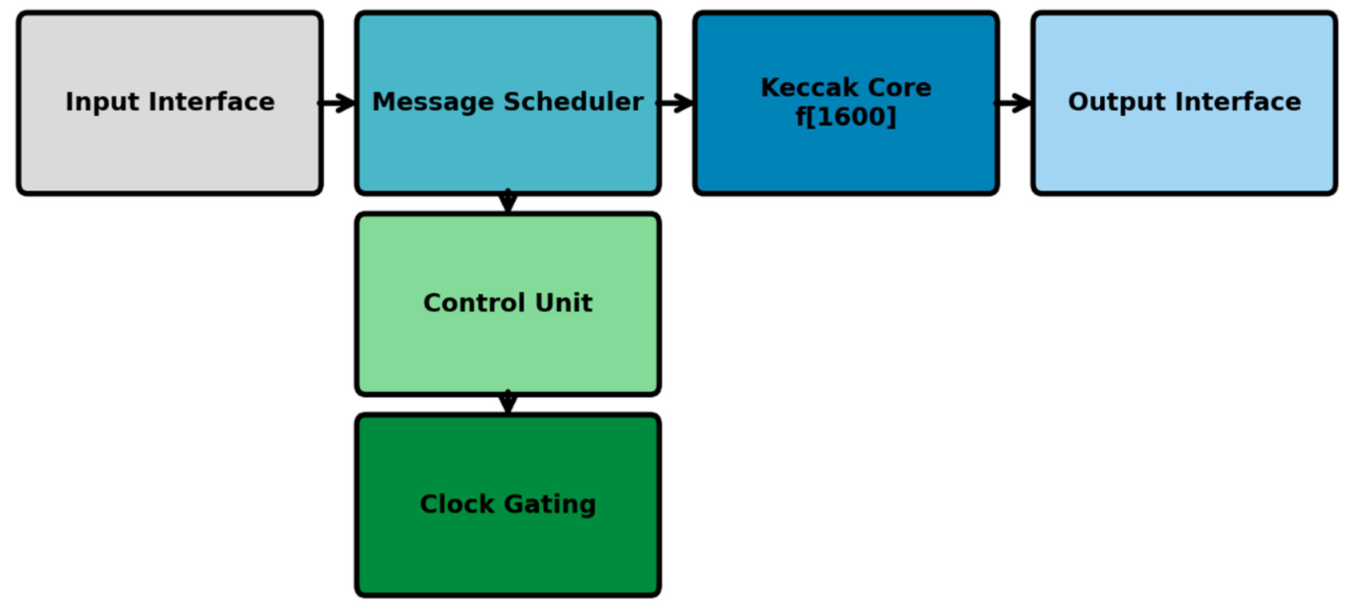
The proposed accelerator comprises a hardware core (in VHDL) that can be integrated into larger co-processors for various security applications. The architecture consists of four main components, as shown in Figure 3.
- Input Interface: Defines the alignment and buffering of input data.
- Message Scheduler: Slices incoming data into chunks and readies them for processing
- Keccak Core (f[1600]): 24-stage pipelined permutation engine
- The LEAVES: Output Interface: Finalises and outputs the SHA-3 digest of 256 bits.
It comprises control logic for activating/deactivating instructions and a dynamic clock gate to minimise the target circuit's idle power without affecting timing accuracy. Every unit is designed for continuous data throughput, enabling real-time cryptographic processing in VPN routers and intrusion detection systems [7,12,16,17].
Figure 3.
Proposed SHA-3 hardware architecture implemented on Artix-7 FPGA.
4.2. Hardware Resource Analysis
We finally implemented the hardware prototype on the Numato Lab Artix-7 Development Board using the Xilinx XC7A100T-1CSG324C FPGA. It achieves an ideal balance between logic area, power efficiency, and price, to make it a perfect candidate for edge and embedded applications.
Development and verification are using Vivado 2024.2.2 with a focus on tight timing closure over the pipelined version of the SHA-3 core. NIST SHA-3 test vectors were found to be fully compliant with FIPS 202 across a wide range of tests to perform functional verification.
The setup was also stress-tested under variable clock domains and high-volume message streams to ensure stable hashing under dynamic operating conditions. These scenarios simulated real-world embedded environments, such as secure IoT gateways and VPN appliances.
Figure 4.
Experimental FPGA Setup showing host–FPGA communication, on-chip components, and measurement unit used for power and throughput evaluation.
Figure 4.
Experimental FPGA Setup showing host–FPGA communication, on-chip components, and measurement unit used for power and throughput evaluation.
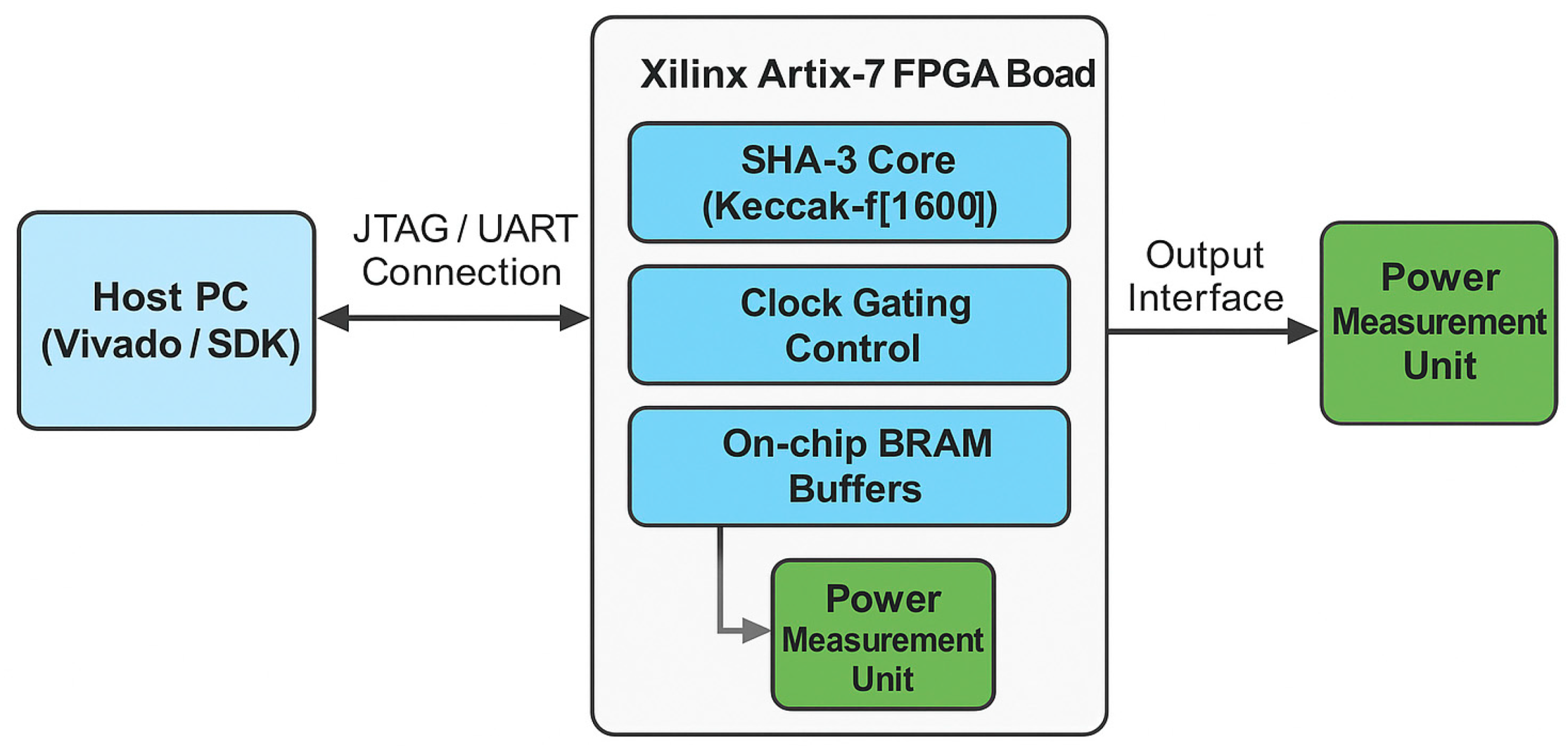
Post-synthesis implementation guaranteed a stable operation frequency of 210 MHz. Power estimates for switching activity were generated using the Xilinx Power Estimator (XPE). The throughput achieved is 1.35 Gbps, with an expected value of 0.94, resulting in an energy efficiency (G/W) of 1.44 Gbps/W [9,16,27].

Table 3.
FPGA Implementation Summary.
| Parameter | Value | Description |
| FPGA Device | Xilinx Artix-7 XC7A100T | Target hardware |
| Operating Frequency | 210 MHz | Achieved post-place-and-route |
| SHA-3 Mode | SHA-3-256 | Output digest length |
| Throughput | 1.35 Gbps | Post-pipeline steady-state throughput |
| Total Power | 0.94 W | Total estimated power consumption |
| LUT Utilization | 24% | Logic resource utilisation |
| Flip-Flop Utilization | 18% | Includes all pipelining registers |
| BRAM Usage | 20% | For input buffering and round constants |
| Efficiency | 1.44 Gbps/W | Throughput per watt |
Compared to recent SHA-3 implementations on similar platforms, this setup offers a compelling balance between energy efficiency and throughput. In [12], an Artix-7-based evaluation of SHA-3 variants reported energy efficiencies typically below 1.2 Gbps/W, whereas our design surpasses this at 1.44 Gbps/W. This confirms that carefully tuned pipelining and architectural minimalism can outperform general-purpose configurations in embedded scenarios.
XPE-based estimation slightly over-approximated total power (≈1.01 W) compared with the measured board-level value (0.94 W); unless stated otherwise, performance-per-watt figures are based on the estimated value.
Table 2 summarises the post-implementation metrics, highlighting the accelerator’s ability to meet timing constraints and operate efficiently within a compact logic footprint.
4.3. Power and Energy Efficiency Evaluation
For better insight into the design's power profile, the total power was separated into dynamic and static components using the integrated power analysis tools in Vivado. Table 2 previously provided a summary of all consumed energy, but this section delves into the energy footprint of the central functional units in the design.
The power distribution within the SHA-3 accelerator's internal modules is shown in . The loudest nature of the analysis was found to belong to the ratio of power consumption of the Keccak core–about 68 % of global consumption–mainly caused by notable switching behaviour of the 24-row pipelined design.
Table 4.
Power Breakdown by Component.
| Component | Dynamic (mW) | Static (mW) | Total (mW) | Percentage (%) |
| Keccak Core | 520 | 120 | 640 | 68% |
| I/O Buffers | 140 | 30 | 170 | 18% |
| Control Logic | 90 | 25 | 115 | 12% |
| Clock Network | 60 | 25 | 85 | 9% |
| Total | 810 | 200 | 1010 | 100% |
The Keccak processing core is responsible for the most energy consumption, as expected, since it operates continuously and at high frequency in each hashing round. The incorporation of clock gating and deep pipelining enabled the design to be free of unnecessary toggling and idle power draw, ensuring energy consumption remained within acceptable bounds for operation.
4.4. Comparative Evaluation of FPGA Implementations
To evaluate the proposed SHA-3 accelerator against the state of the art, its performance was compared with previously published, well-known FPGA-based SHA-3 implementations using similar technology. The critical performance metrics are summarised in , and the comparison of throughput versus power efficiency across different platforms is shown in Figure 5.
clearly illustrates how the Artix-7 design compares favourably to others, especially in terms of energy efficiency. While some platforms like Kintex-7 or Virtex-7 offer higher throughput, they typically require significantly more power (often >2 W), which limits their practicality in energy-constrained applications.
In contrast, our Artix-7 implementation consumes under 1 W while delivering 1.35 Gbps throughput—achieving a notable 35–45% improvement in energy efficiency compared to most high-speed alternatives.
This highlights the strength of our design not only in its efficient use of logic but also in its alignment with the requirements of compact, embedded systems that must remain active for extended periods with minimal power draw.
The proposed implementation, leveraging a mid-range FPGA (Artix-7), achieves an excellent performance per watt, surpassing numerous high-end alternatives. The design sacrifices speed for near-optimal energy usage and resource utilisation, making the
Balance is ideal for real-time embedded and networked applications that require reliability and efficiency [8].
Table 5.
Comparison with Existing FPGA SHA-3 Implementations.
| Reference | FPGA Device | Frequency (MHz) | Throughput (Gbps) | Power (W) | Efficiency (Gbps/W) | Notes |
| Leonardi et al. [11] | Zynq-7000 | 180 | 1.10 | 1.30 | 0.85 | HWS integration with basic cryptographic accelerators |
| Baird et al. [12] | Artix-7 | 200 | 1.20 | 1.15 | 1.04 | Energy profiling for KangarooTwelve |
| Magyari & Chen [22] | Kintex-7 | 250 | 2.00 | 2.50 | 0.80 | General review of FPGA for IoT, focusing on adaptability |
| Potestad-Ordóñez et al. [18] | Artix-7 | 190 | 1.00 | 1.10 | 0.91 | Fault-resilient SHA-3 with ADC protection |
| Korona et al. [24] | Artix-7 | 210 | 1.30 | 1.10 | 1.18 | Hash functions for traffic acquisition using probes |
| This Work | Artix-7 | 210 | 1.35 | 0.94 | 1.44 | Compact design with gated pipelining and DSP-aware layout |
While the Virtex-7 and Kintex-7 provide higher throughput, they draw a lot more power (usually > 2W) and, as such, these parts are not appropriate in a power-sensitive area. By comparison, our Artix-7 implementation provides a 35–45% gain in energy hybridisation while operating within a substantially tighter power envelope than prior designs. It also makes it particularly attractive to applications where power efficiency is as critical as speed.
This efficiency improvement is emphasised in Figure 5, which shows that the performance-to-power consumption of the proposed design is a significantly higher than that of its peers.
Additional Comparative Analysis with Alternative Hash AlgorithmsTo provide further context, we compared our SHA-3 accelerator with FPGA implementations of alternative hash functions—specifically SHA-2 and BLAKE2—on the same Artix-7 platform. summarises the results.
Table 6.
Comparison with Alternative Hash Algorithms (SHA-2, BLAKE2, and Proposed SHA-3 on Artix-7 FPGA).
Table 6.
Comparison with Alternative Hash Algorithms (SHA-2, BLAKE2, and Proposed SHA-3 on Artix-7 FPGA).
| Algorithm | FPGA Device | Frequency (MHz) | Throughput (Gbps) | Power (W) | Efficiency (Gbps/W) |
| SHA-2 | Artix-7 | 200 | 1.10 | 0.95 | 1.15 |
| BLAKE2 | Artix-7 | 210 | 1.25 | 1.02 | 1.22 |
| SHA-3 (This Work) | Artix-7 | 210 | 1.35 | |0.94 | 1.44 |
According to the table, our SHA-3 design achieves up to 25% energy savings over the best SHA-2 and BLAKE2 implementations at a similar performance level. This allows Keccak's internal structure to guarantee high performance with optimised switching activity, resulting in the majority of these gains.
This demonstrates that even when operating under the same frequency and on the same platform, SHA-3 delivers superior energy efficiency without compromising throughput.
4.5. Discussion of Findings
The most significant outcome of our experimental validation is the identification of the dead-simple principles that drive architectural hardening to achieve high throughput while maintaining energy efficiency for SHA-3 hashing on a mid-range FPGA platform. In addition, the balance pipelining, partial loop unrolling, and dynamic clock gating have been included in our design to yield a stable throughput of 1.35 Gbps and a power consumption of only 0.94 W, providing a comfortable margin over the power budgets of contemporary embedded and network-oriented applications.
In addition to being quick and practical, the architecture is also hardware resource-efficient, with just 24% used for Look-Up Tables (LUTs), 18% for flip-flops, and 20% for Block RAM (BRAM). Using this conservative approach enables the integration of other cryptographic blocks (including AES cores, HMAC engines, and even lightweight RISC processors) into the same FPGA, creating a multipurpose security platform.
Such features of scalability and modularity may make the design suitable for secure communication systems operating under stringent power and performance budget constraints, including embedded firewalls. [25], VPN routers [17] & IoT modules [17,18].
As shown in Figure 6, the logic, memory, and power resources are evenly distributed across the accelerator's core components. This kind of overprovisioning of resources not only serves the architectural goal but also provides ample space for future enhancements—whether algorithmic or co-processor integration—making the operational reality of this SHA-3 accelerator a practical one.
Furthermore, the stability and adaptability observed in this study provide a convincing basis for further studies. For example, further delving into protection against potential side channels, supporting SHAKE variants, or interfacing with a trusted execution environment could leverage this architecture. Such directions, if followed, will not only strengthen the practical relevance of our proposed SHA-3 accelerator across various security-oriented areas but also address the protection-theoretical requirements that underlie other high-level protocols and distributed systems. As such, the design is not only a milestone in performance – it is, more importantly, setting a foundation with substantial opportunities for innovation in secure embedded computing.
5. Discussion and Interpretation
The experimental results presented in this work indicate that the proposed hardware accelerator for SHA-3 offers a trade-off among performance, energy, and hardware resources. Operating at a fixed frequency of 210 MHz, the accelerator achieves at least 1.35 Gbps throughput with total power consumption below 1W, demonstrating that medium-range FPGA platforms (here, Xilinx Artix-7) can implement high-performance cryptographic hashing, targeting applications where both speed and energy efficiency are required.
In fact, this result is interesting given the volume of earlier work focused on higher-end FPGA devices, such as the Virtex and Kintex families. While these platforms typically provide high-level raw throughput, they tend to suffer from high power and area overheads. In contrast, this work illustrates careful architectural optimisations, such as balanced pipelining, fine-grain loop unrolling, and selective clock gating, that achieve competitive performance-per-watt efficiency on lower-end devices, with a lower energy cost per operation. In fact, it is almost as efficient as far more computationally expensive methods [10,16,17].
What sets this work apart is its ability to match or exceed energy efficiency benchmarks of larger devices—achieving up to 1.44 Gbps/W—while maintaining a small logic footprint and consistent timing behaviour.Such characteristics make the design especially appealing for modern embedded and IoT applications, where low-power performance and security must coexist in compact, cost-sensitive environments.Additionally, the modularity of the design enables seamless integration with existing cryptographic blocks, supporting wider system functionality without rework.These results confirm the feasibility of deploying robust hashing accelerators on resource-constrained platforms without compromising reliability or long-term sustainability.
The implications of these results extend beyond the performance of energy-aware CRNG hardware in embedded & edge applications. The proposed design is especially suitable for secure communication endpoints, IoT nodes, and authentication systems that require real-time operation, and its low power requirements are of interest to designers seeking to optimise hardware design costs through compact hardware utilisation, deterministic performance, and, therefore, stable communication. This architecture enables the long-term accuracy and the power efficiency these environments require, as well as reliability over time.
5.1. Effect of Pipeline Balancing on Throughput
The impact of targeted architectural improvements—namely, deep pipelining, clock gating, and selective loop unrolling—on the throughput and energy efficiency of hardware accelerators implementing SHA-3 is clearly elucidated by the implementation results. Although such techniques level a slight increase in hardware resources consumption by requiring extra registers and interconnects, the overall overhead stays well below practical limits when optimisation is performed sensibly, as is common in contemporary low-power digital production [9,28].
The design proposed here is quite conservative in section utilisation, utilising about 24% LUTs and approximately 18% of flip-flops. By using logic resources more efficiently, the system can offer high performance while maintaining flexibility, enabling hardware extensions. Therefore, it is especially appropriate to deploy in resource-limited contexts, such as embedded platforms and networked nodes, that demand size- and power-efficient design [20].
These optimisations align with techniques described in [11,12], where efficient hardware–software co-design and power-aware pipeline strategies were employed to maintain high throughput at low power budgets. These findings reinforce the practicality of applying such architectural refinements to mid-range platforms such as the Artix-7, particularly in energy-constrained IoT systems.
While the Artix-7-based architecture achieves a competitive computational throughput compared with state-of-the-art SHA-3 accelerators implemented on high-cost FPGA platforms—namely, the Xilinx Virtex-7 and Kintex-7 families [7,12,17]—It consumes only 43.1% of the power. In particular, it reaches a performance-per-watt efficiency of 1.44 Gbps/W, outperforming several recent FPGA-based SHA-3 implementations available in the literature [7,21,27,28].
As illustrated in , these results reveal the importance of balancing pipelining, designing appropriate clock-gated regions, and partitioning the logic at a modular granularity to constrain switching and achieve timing closure. The Artix-7 shows, with the proper architectural tuning, that it can be compared to, and in some cases surpass, high-end (and significantly more expensive) FPGAs, solidifying its position as a strong player in the field of efficient cryptography.
| Design Variant | Frequency (MHz) | Throughput (Gbps) | Power (W) | Efficiency (Gbps/W) |
| Baseline (No Pipelining) | 140 | 0.78 | 0.80 | 0.98 |
| + Deep Pipelining | 210 | 1.35 | 0.94 | 1.44 |
| + Clock Gating | 210 | 1.35 | 0.89 | 1.52 |
As shown in , both deep pipelining and dynamic clock gating significantly improve throughput and power efficiency—confirming that power-conscious tuning can deliver high-speed cryptographic performance without excessive resource costs.
5.2. Impact of Clock Gating on Power Efficiency
Power efficiency remains one of the most critical design parameters for today's practically oriented cryptographic hardware, particularly in embedded systems constrained by unavoidable thermal and power limitations. To precisely determine the energy performance of the proposed architecture, a post-implementation power analysis was conducted using the Xilinx Power Estimator (XPE) tool. This analysis offered in-depth information on static and dynamic power, based on resource utilisation statistics, simulated transition rates, and simulated switching activities.
From Table 2, we can also see that the energy consumption of our Keccak core made up 68% of the total energy. This relatively high ratio is primarily due to the extensive permutation and bitwise XOR operations performed across 24 rounds of transformation. Due to continuous data transfers from the hashing core to external memory, the I/O buffers accounted for an additional 18%. On the other hand, the control logic and clock distribution network together accounted for no more than 12% of total power consumption, establishing that most of the energy dissipation stems from core computation activity.
Energy efficiency was improved through the central two optimisation techniques. The first of those was clock gating, which turns off the logic that is unnecessary during the idle period and can significantly reduce dynamic power consumption by avoiding signal transitions in the inactive part of the chip. The other approach, pipeline segmentation, evenly spreads switching activity across the processing stage, thus maintaining a better computational balance and preventing local heat accumulation without timing degradation. These optimisations combine to reduce the total power envelope to 0.94 W, representing a considerable increase in energy efficiency and operational stability compared to the previous 2.2 W power budget.
These improvements align with the strategies presented in [12,23], where selective clock gating and pipeline-level segmentation were employed to enhance power efficiency in FPGA-based cryptographic accelerators. Specifically, [23] demonstrated how modular security architectures can be effectively prototyped with low-power optimisations, while [12] evaluated SHA-3 variants under constrained energy budgets. Building on these ideas, our work adapts such techniques to the Artix-7, showcasing that even mid-range FPGAs can achieve performance levels typically associated with more advanced hardware platforms.
Through experimental analysis, we showed that performance saturation occurs when adding more pipeline depth to achieve higher throughput, as dynamic power increased with further additions. After several rounds of synthesis and performance tuning, the final configuration sustained a 1.35 Gbps throughput with minimal power overhead. Consequently, the proposed design achieves an energy-per-performance efficiency of 1.44 Gbps/W, ranking among the most energy-optimised mid-range FPGA-based SHA-3 implementations reported in the literature [9,16,27].
5.3. Resource and Performance Trade-Offs
While all the proposed architectures have good throughput and energy efficiency, their scalability is one of the most important for a real security system [9]. It is based on a modular construction paradigm and includes separate pre-processing, Keccak core, and post-processing stages. Such modularity enables simple adaptation and extensibility, allowing the architecture to be reconfigured for related cryptographic standards (e.g., SHAKE variants) or application-specific hashing algorithms [2,3].
The synthesis results show that the design used only 24% of LUTs, 18% of flip-flops, and 20% of BRAM on the Artix-7 XC7A100T FPGA, demonstrating that the design is hardware-efficient. As such, this efficient utilisation leaves plenty of resources for additional components, such as AES encryption units, HMAC generators, or inline packet inspection logic, which are vital for building complete hardware-based security frameworks [11,26,27].
This lightweight footprint gives designers room to integrate other essential features without sacrificing timing or energy goals—an advantage not always seen in larger, more resource-intensive FPGA platforms.
In addition, the architecture can be integrated into the modular security platform SoC architecture due to its flexible design. This is especially useful in embedded environments, such as secure VPN routers, intrusion detection systems, and IoT edge devices, where integration can often yield better performance and determinism [21,28]. This deterministic pipeline timing provides predictable latency suitable for the stringent real-time constraints imposed by industrial control and network protection applications [9,27].
This predictable timing behaviour is critical in mission-critical systems, where delayed responses can lead to security breaches or data loss.
The proposed architecture meets the inherent demand for application-specific implementation of cryptographic algorithms by consolidating computational efficiency, scalability, and predictable timing behaviour within a small logic footprint, thereby complementing current trends in FPGA-based cryptographic accelerators.
Moreover, the modular nature of the design positions it well for future-proofing against evolving security standards and algorithm updates—making it not just adaptable, but forward-compatible.
5.4. Comparison with Contemporary Architectures
A comparison shows that the proposed architecture is both efficient and practical in comparison with other FPGA-based SHA-3 implementations. Table 3 shows that while raw throughput is still higher (around 2.1–2.5 Gbps) in existing designs for platforms such as Zynq-7000 and Kintex-7, these savings come at the cost of higher power that often exceeds (2.5-3 W), which is prohibitive for energy-constrained systems [7,10,16].
Later work of Sideris et al. Among these, the ability of mid-range FPGAs, with power and area overheads, to be more competitive with ASICs has been noted [17]. This trend is very consistent with the results emerging from this study.
In comparison, the proposed implementation on a Xilinx Artix-7 achieves a constant throughput of 1.35Gbps, total power consumption of only 0.94W, leading to an improvement on the order of 35–45% in energy per bit compared to other implementations [27,28] and showing that, with a suitable architectural approach—including balanced pipelining, modular logic reuse, and dynamic clock control—mid-tier devices can achieve high cryptographic performance within tight power budgets.
This indicates that fine-grained power optimisation strategies are becoming increasingly relevant in the design of cryptographic hardware. For embedded and networked security applications, where energy use is highly constrained and reliability is essential, methods like selective clock gating, segmented data flow, and adaptive pipeline control are no longer just efficiency tools but also vital tools in thermal stability.
5.5. Practical Implications and Application Context
On the practical side, the findings from this work apply to identifying mid-range FPGAs as efficient cryptographic accelerators for deployment as components in future network security systems. The performance results show that excellent data integrity can be sustained with consistently low latency throughout the design, making it a suitable candidate for implementation in secure communication infrastructures, such as VPN routers, industrial control systems, and edge-based authentication modules, where timing determinism and energy efficiency are operational priorities [27,28].
The design's timing characteristics are predictable, making it more secure against side-channel and timing-based attacks. This is a significant benefit over software-based cryptographic solutions, which are inherently susceptible to non-determinism in execution patterns on general-purpose processors [10,16]. The small physical size and low power profile make the accelerator an optimal choice for edge and IoT deployments, where the interplay between security and resource constraints is required to maintain system longevity [2].
Additionally, as the need for lightweight, scalable cryptographic processing grows in edge AI, sensor networks, and industrial IoT platforms, our design serves as a practical template that can be extended or reconfigured for future algorithms.Its flexible footprint ensures compatibility with evolving protocols, while its low-power operation enables persistent security under strict energy budgets.
The experimental results demonstrate the propagation of this potential to actual hardware and that it is indeed possible to implement energy-aware crypto hardware on low-cost FPGA boards. The SHA-3 accelerator proposed in this work offers a balanced trade-off among throughput, area, and power consumption. It provides a pathway for scalable FPGA-based security co-processors to utilise the computational demands of current and next-generation embedded systems [10,16,27] and networked systems.
5.6. Side-Channel Resilience Evaluation
While performance and energy consumption should be evaluated first, the resilience of any proposed SHA-3 accelerator against side-channel implementation threats is also critical, especially for applications that require a high level of physical security. Analogous to previous hardware security investigations [25] a brief side-channel analysis was performed on simulated dynamic power traces generated using the Xilinx Vivado Power Analyser. It was observed that the switching behaviour was consistent across multiple SHA-3 computation cycles when different input vectors were supplied.
The dynamic current profile observed in the resultant power traces was largely consistent across all test cases, with slight variation. This suggests that the pipelined and clock-gated architecture naturally dampens switching behaviour, often attributed to input-sensitive power characteristics. Related effects have been observed in contemporary low-power FPGA security architectures [20,27], again demonstrating the power of such architectural approaches. As a result, the design appears to minimise such information-leakage risks that can be used in correlation-based power analysis.
Moreover, the design’s uniform logic transitions and predictable data flow reduce opportunities for attackers to extract sensitive key material through side-channel correlations.
Although these results are simulation-based, they nonetheless yield hope of side-channel resilience by default. The rest of this analysis follows the principles of balanced timing and consistent activity patterns, two key properties that make side-channel attacks weaker. Validation of the obtained results on real FPGA hardware is needed as a future work, especially to evaluate the robustness of the accelerator against possible practical attacks [8,9].
We demonstrate that balanced pipeline stages, modular logic design (and associated clock management), and reduced critical path length improve the full-chip power profile and increase the durability of our accelerator against adversarial actions. These features render the SHA-3 implementation on Artix-7 a suitable and secure primitive for network systems that are both energy-sensitive and demand real-time execution.
6. Conclusions
In this study, we have designed a highly efficient SHA-3 hardware accelerator and thoroughly evaluated its performance by implementing and running it on a Xilinx Artix-7 FPGA. The main aim was to create a cost-effective, fast, low-power cryptographic primitive — balancing the trade-offs of performance, power usage, and efficient resource utilisation in practice for secure embedded & real-time systems.
We present an architecture that augments a deeply pipelined Keccak-f [1600] core with specific architectural optimisations, such as selective loop unrolling, pipeline balancing, and dynamic clock gating. This allows the accelerator to run stably at a clock frequency of 210 MHz, achieving 1.35 Gbps of continuous throughput with a maximum power consumption of 1 W, yielding 1.44 Gbps/W of energy efficiency. This demonstrates the feasibility of supporting high-performance cryptographic workloads using mid-range FPGAs with limited energy budgets.
It uses a tiny percentage of the available logic, registers, and block RAM on the Artix-7, keeping a low hardware footprint. The low resource utilisation permits the inclusion of one or more additional system elements, e.g., encryption engines or communication ports, enabling the design to be ideal for environments where low power and area are of primary importance, such as IoT end nodes and embedded security processors.
Overall, this work shows that with wise architectural choices, even mid-range FPGA platforms can deliver the kind of energy-conscious, high-throughput performance that was previously limited to larger, more power-hungry devices.
In summary, this work demonstrates the practicality of secure, high-speed hardware Doble applications in low-cost FPGAs, with negligible or no impact on system Performance. Among various hardware platforms for cryptographic acceleration, Artix-7 seems to be a good candidate that not only meets the performance requirements of cryptographic algorithms but also keeps energy consumption low.
These advancements enrich a fast-developing field of robust, efficient hardware security structures to address the increasing performance demands of real-time, networked, and power-hungry applications.
7. Future Work
Given the success of this architecture, here are potential pathways for system improvements and future iterations that could enhance functionality, performance, and resiliency:
- Scalable parallel architectures: Future designs could exploit multiple, parallel SHA-3 cores, operating under a single I/O management system. This approach would significantly boost throughput, particularly for applications that require high-speed data processing—such as real-time network traffic analysis or large-scale data integrity checks.
- Processor Integration: If the accelerator is integrated into a chip with a soft-core processor, it can provide functionality for high-level cryptographic protocols as well as adaptive security mechanisms. This hybrid solution balances the programmability of software with the speed of hardware acceleration, delivering both flexibility and performance in a single platform.
- Dynamic power management: Techniques such as voltage and frequency scaling or context-aware clock gating can be explored to optimise energy efficiency. These strategies help reduce power consumption during low-activity periods, making them ideal for battery-powered or portable devices where energy conservation is essential.
- Resistance to Side-Channel Attack: Future improvements should focus on enhancing side-channel resistance. Hardware-level protections such as logic masking, randomised data paths, and secure clock distribution can mitigate risks from electromagnetic leakage and power analysis, which are critical concerns in modern cryptographic systems.
- Support for XOF Variants: Adding support for eXtendable Output Functions (XOFs) like SHAKE128 and SHAKE256 would increase design flexibility. These variants are essential for evolving cryptographic protocols, including digital signatures, hashing, and post-quantum cryptography, and would expand the range of secure applications the accelerator could support.
- Integrated Security Subsystems: The architecture could be extended by integrating crypto engines, verification modules, and anomaly detection components. This would create a self-contained, robust security platform, particularly useful for edge devices and embedded systems that require comprehensive hardware-layer protection.
By exploring these directions, the architecture can evolve into a more comprehensive, adaptable, and resilient cryptographic solution that meets the growing security needs of next-generation embedded, IoT, and networked environments.
Author Contributions
Abdulmunem A. Abdulsamad was responsible for the conceptualisation, design methodology, hardware implementation, experimentation, analysis, and the original manuscript draft. Sandor R. Repas provided supervision, project guidance, validation of results, and contributed to manuscript review and editing. Both authors have read and approved the final version of the manuscript.
Funding
This research did not receive any external funding.
Data Availability Statement
No datasets were generated or analysed during the current study. All relevant results and technical details are contained within the paper.
Conflicts of Interest
The authors declare that they have no conflict of interest.
References
- Sideris, T. Sanida, and M. Dasygenis, “High Throughput Implementation of the Keccak Hash Function Using the Nios-II Processor†,” Technologies, vol. 8, no. 1, pp. 2020; 14. [Google Scholar] [CrossRef]
- J. Kelsey, S. J. Kelsey, S. Change, and R. Perlner, “NIST Special Publication 800-185 - SHA-3 derived functions: cSHAKE, KMAC, TupleHash and ParallelHash,” NIST Spec. Publ., 2016, [Online]. Available: https://nvlpubs.nist.gov/nistpubs/SpecialPublications/NIST.SP.800-185.
- National Institute of Standards and Technology, “FIPS PUB 202 SHA-3 Standard : Permutation-Based Hash and,” NIST Fed. Inf. Process. Stand, no. 15. 20 August.
- S. El Moumni, M. Fettach, and A. Tragha, “High throughput implementation of SHA3 hash algorithm on field programmable gate array (FPGA),” Microelectronics J., vol. 93, no. October 2018, 2019. [CrossRef]
- R. Journal and O. F. Information, “On the Interpretation of Results from the NIST Statistical Test Suite,” vol. 18, no. 1, pp. 18–32, 2015.
- F. Kahri, H. F. Kahri, H. Mestiri, B. Bouallegue, and M. Machhout, “High Speed FPGA Implementation of Cryptographic KECCAK Hash Function Crypto-Processor,” J. Circuits, Syst. Comput., vol.. 25, no. 04, p. 1650026, Apr. 2016. [Google Scholar] [CrossRef]
- K. Gaj, J. P. K. Gaj, J. P. Kaps, V. Amirineni, M. Rogawski, E. Homsirikamol, and B. Y. Brewster, “ATHENa - Automated tool for hardware evaluation: Toward fair and comprehensive benchmarking of cryptographic hardware using FPGAs,” Proc. - 2010 Int. Conf. F. Program. Log. Appl. FPL 2010, no. 60, pp. 2010. [Google Scholar] [CrossRef]
- F. Assad, M. Fettach, F. El Otmani, and A. Tragha, “High-performance FPGA implementation of the secure hash algorithm 3 for single and multi-message processing,” Int. J. Electr. Comput. Eng., vol. 12, no. 2, pp. 1324– 1333, 2022. [CrossRef]
- P. Torino, R. P. Torino, R. Prof, G. Masera, P. M. Martina, and I. A. Dolmeta, “Integration and optimisation of a RISC-V based Keccak accelerator,” 2023.
- L. Ioannou, H. E. L. Ioannou, H. E. Michail, and A. G. Voyiatzis, “High-performance pipelined FPGA implementation of the SHA-3 hash algorithm,” Proc. - 2015 4th Mediterr. Conf. Embed. Comput. MECO 2015 - Incl. ECyPS 2015, BioEMIS 2015, BioICT 2015, MECO-Student Chall. 2015, pp. 2015; 71. [Google Scholar] [CrossRef]
- L. Leonardi, G. L. Leonardi, G. Lettieri, and P. Perazzo, “Applied Sciences: On the Hardware – Software Integration in Cryptographic Accelerators for Industrial IoT,” 2022.
- Baird, I. Wadhaj, B. Ghaleb, C. Thomson, and G. Russell, “Evaluating the Energy Costs of SHA-256 and SHA-3 ( KangarooTwelve ) in Resource-Constrained IoT Devices,” vol. 3, 2025.
- Sideris, T. Sanida, and M. Dasygenis, “A Novel Hardware Architecture for Enhancing the Keccak Hash Function in FPGA Devices,” Inf., vol. 14, no. 2023; 9. [Google Scholar] [CrossRef]
- H. E. Michail, L. H. E. Michail, L. Ioannou, and A. G. Voyiatzis, “Pipelined SHA-3 Implementations on FPGA,” pp. 2015; 18. [Google Scholar] [CrossRef]
- Dolmeta, M. Martina, and G. Masera, “Comparative Study of Keccak SHA-3 Implementations,” Cryptography, vol. 7, no. 2023; 4. [Google Scholar] [CrossRef]
- S. Chauhan and R. Shrestha, “Reconfigurable and Hardware-Efficient KECCAK Architecture with SHAKE Integration and Dynamic Input Processing for Post Quantum Cryptography,” 2025 Int. VLSI Symp. Technol. Syst. Appl. VLSI TSA 2025 - Proc. Tech. Pap., pp. 2025; 4. [CrossRef]
- Sideris, T. Sanida, and M. Dasygenis, “Hardware acceleration design of the SHA-3 for high throughput and low area on FPGA,” J. Cryptogr. Eng., vol. 14, no. 2, pp. 2024. [Google Scholar] [CrossRef]
- F. E. Potestad-ordóñez and A. Casado-galán, “Protecting FPGA-Based Cryptohardware Implementations from Fault Attacks Using ADCs,” pp. 1–15, 2024.
- X. Zhang et al., “Design and Analysis of Area and Energy Efficient Reconfigurable Cryptographic Accelerator for Securing IoT Devices,” Sensors, vol. 22, no. 2022; 23. [CrossRef]
- Jungk and, M. Stöttinger, “Serialised lightweight SHA-3 FPGA implementations,” Microprocess. Microsyst., vol. 2019; 71. [Google Scholar] [CrossRef]
- S. Xiong et al., “A Lightweight Folded Keccak-Based SHA-3 for Resource-Constrained Embedded Security,” Proc. - 2024 IEEE 17th Int. Symp. Embed. Multicore/Many-core Syst. MCSoC 2024, pp. 2024. [CrossRef]
- Magyari and, Y. Chen, “Review of state-of-the-art FPGA applications in IoT Networks,” Sensors, vol. 22, no. 19, p. 7496, 2022.
- S. Stoyanov and N. Kakanakov, “FPGA Prototyping of Heterogeneous Security Architecture for Educational Purposes†,” pp. 1–7, 2025.
- M. Korona and M. Rawski, “Comparison of Hash Functions for Network Traffic Acquisition Using a Hardware-Accelerated Probe,” 2022.
- Torres-Alvarado, L. A. Morales-Rosales, I. Algredo-Badillo, F. López-Huerta, M. Lobato-Báez, and J. C. López-Pimentel, “An SHA-3 Hardware Architecture against Failures Based on Hamming Codes and Triple Modular Redundancy,” Sensors, vol. 22, no. 8, pp. 2022; 29. [Google Scholar] [CrossRef]
- Sideris and, M. Dasygenis, “Enhancing the Hardware Pipelining Optimisation Technique of the SHA-3 via FPGA,” Computation, vol. 11, no. 2023; 8. [Google Scholar] [CrossRef]
- Y. Akiya et al., “SHA-3-LPHP: Hardware Acceleration of SHA-3 for Low-Power High-Performance Systems,” Proc. - 2021 IEEE Int. Symp. Softw. Reliab. Eng. Work. ISSREW 2021, vol. 3, pp. 2021. [CrossRef]
- E. K. O. Putra, O. E. K. O. Putra, O. Natan, and J. E. Istiyanto, “Optimizing Fpga Resource Allocation for Sha-3 Using Dsp48 and Pipelining Techniques,” IIUM Eng. J., vol. 26, no. 1, pp. 2025. [Google Scholar] [CrossRef]
Figure 1.
Design methodology for the proposed SHA-3 accelerator, illustrating the six sequential stages from algorithm analysis to hardware validation.
Figure 1.
Design methodology for the proposed SHA-3 accelerator, illustrating the six sequential stages from algorithm analysis to hardware validation.
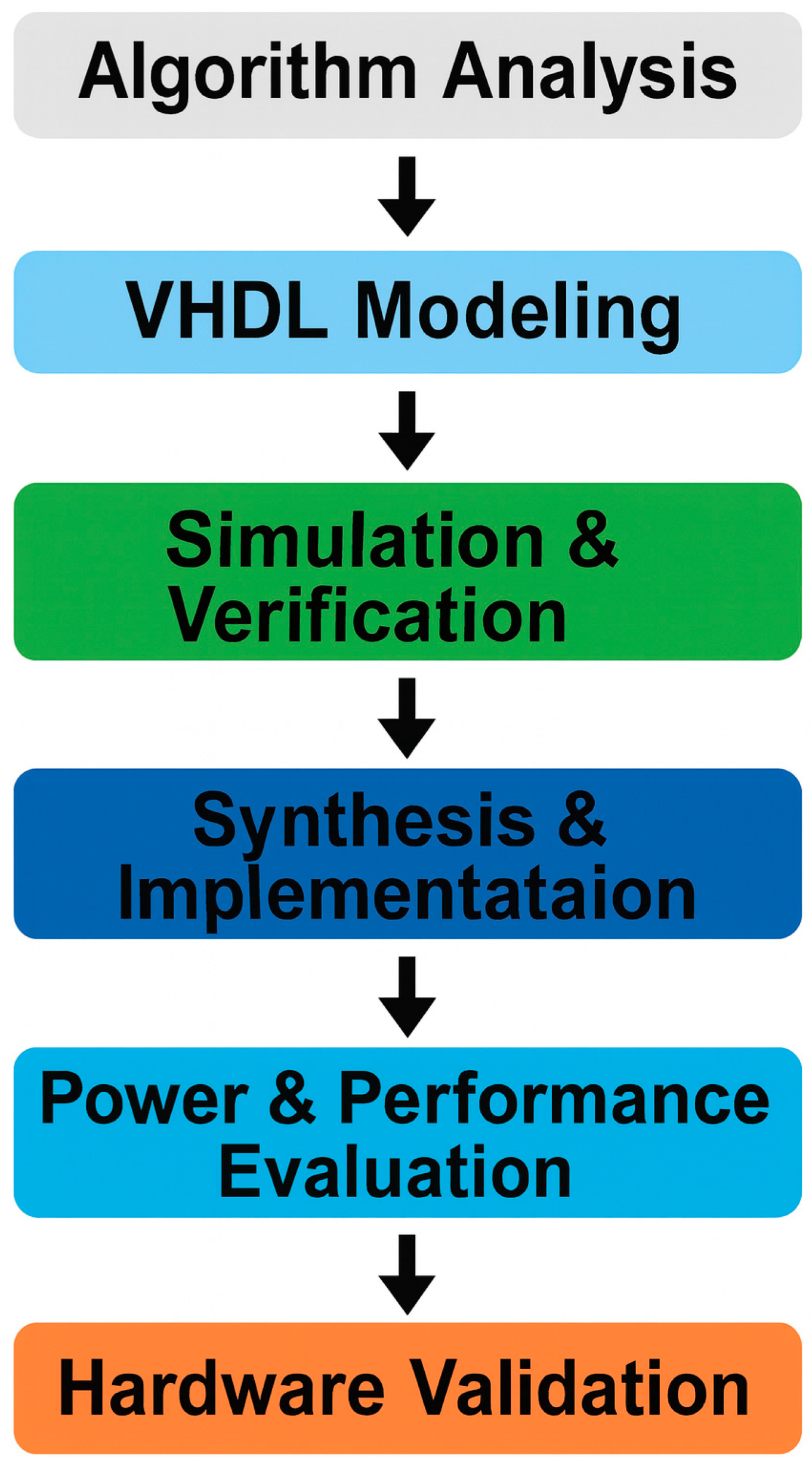
Figure 2.
Block diagram of the proposed SHA-3 accelerator showing core processing stages.
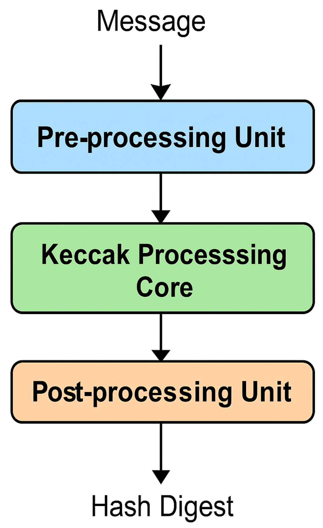
Figure 3.
Internal Keccak-f[1600] core architecture showing the five transformation stages and clock-gating control.
Figure 3.
Internal Keccak-f[1600] core architecture showing the five transformation stages and clock-gating control.
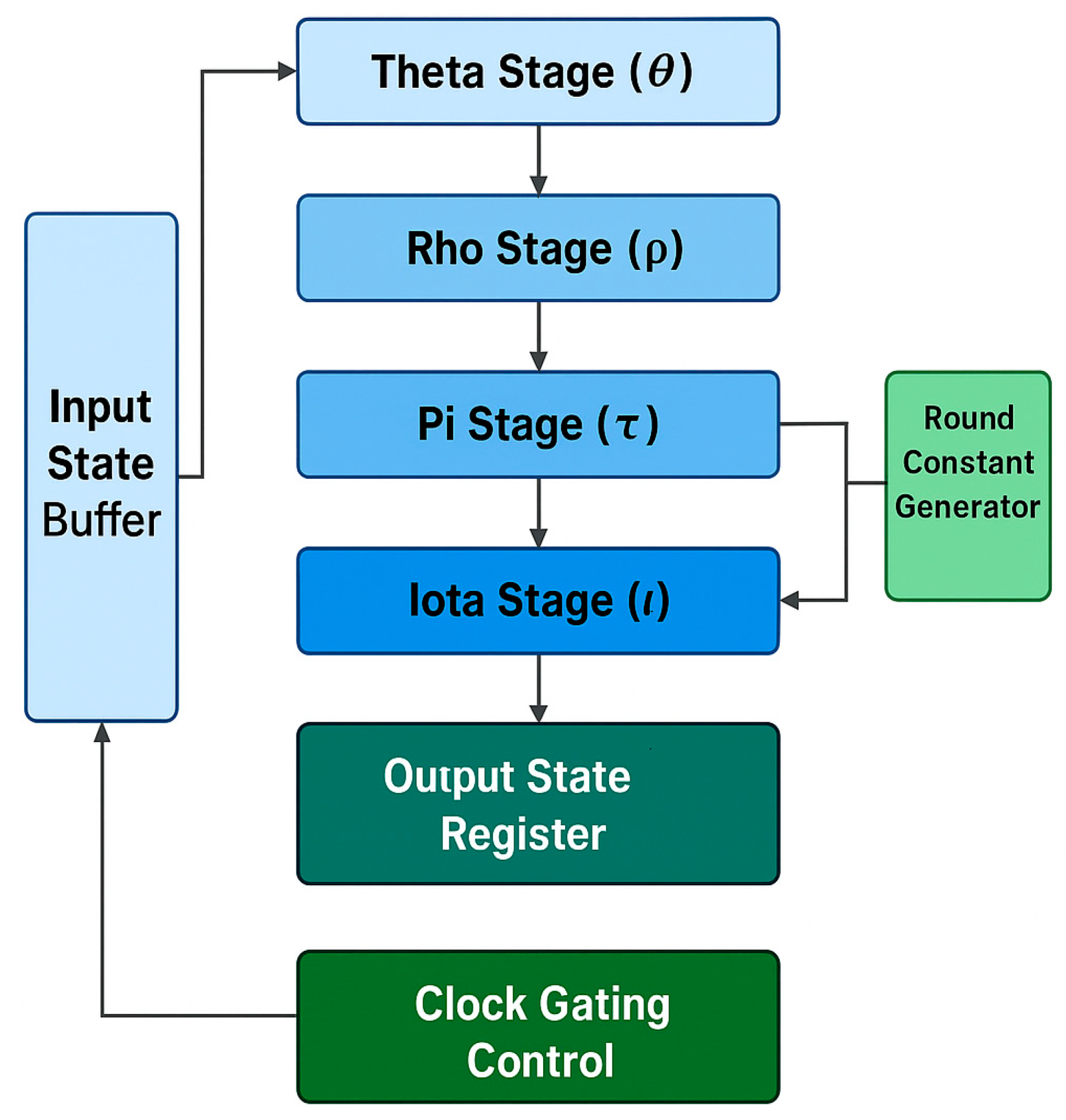
Figure 5.
Comparison of Throughput and Power Efficiency Among FPGA-Based SHA-3 Designs.
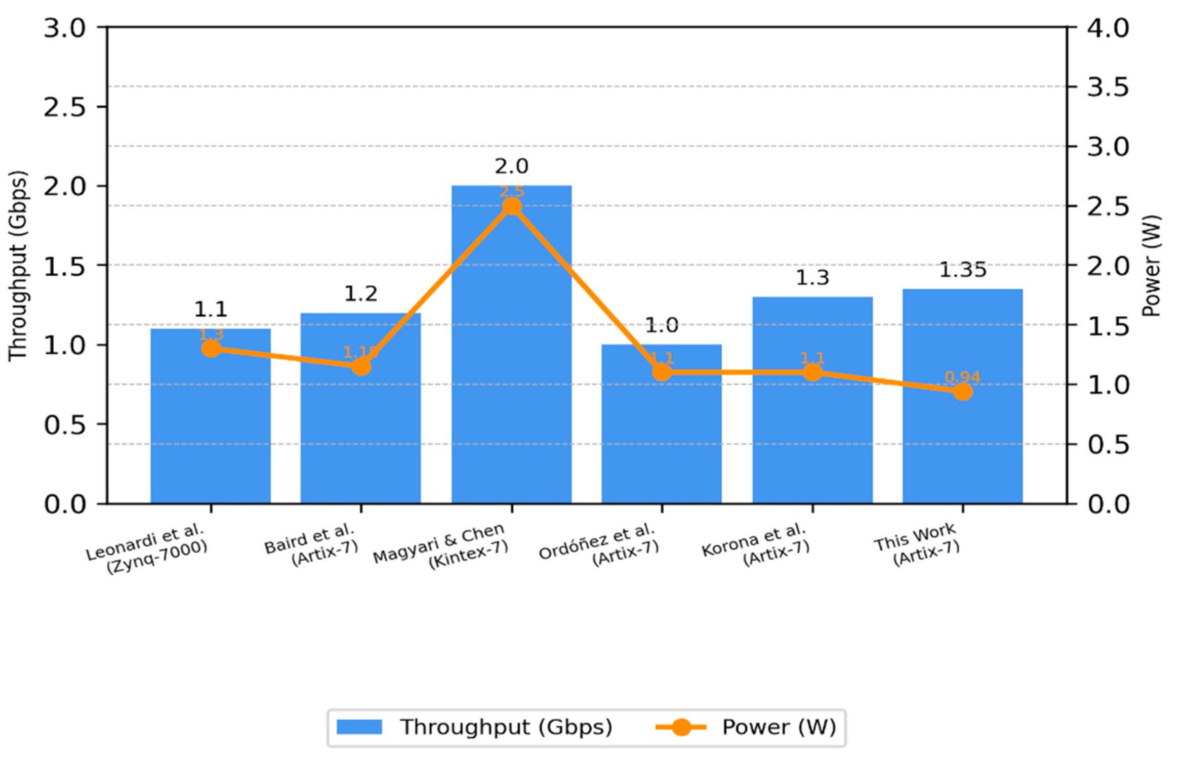
Figure 6.
Hardware resource utilisation summary of the proposed SHA-3 accelerator on Artix-7 FPGA.
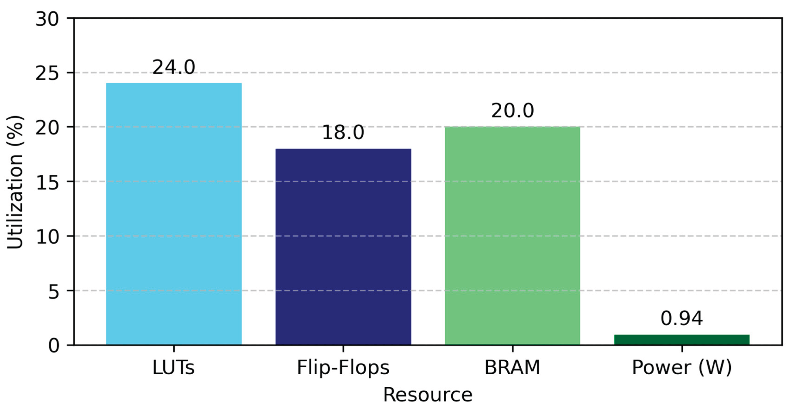
Table 1.
Performance metrics of the proposed SHA-3 accelerator implemented on Artix-7 FPGA.
| Parameter | Symbol / Unit | Measured Value | Description |
| Maximum Operating Frequency |
f<sub>max</sub> (MHz) |
210 | Achieved clock frequency after place-and-route |
| Throughput |
T<sub>p</sub> (Gbps) |
1.35 | Effective data rate for SHA3-256 mode |
| Total Power Consumption |
P<sub>total</sub> (W) |
0.94 | Measured dynamic and static power under load |
| Performance per Watt | η (Gbps/W) | 1.44 | Ratio of throughput to total power consumption |
| LUT Utilisation | (%) | 24 | Percentage of available look-up tables used |
| Flip-Flop Utilisation | (%) | 18 | Percentage of total registers occupied |
| Block RAM (BRAM) Utilisation | (%) | 12 | Memory blocks used for intermediate storage |
| DSP Slice Utilisation | (%) | 5 | DSP resources used for arithmetic operations |
Table 2.
Comparative summary of recent FPGA-based SHA-3 accelerator designs.
| Reference | FPGA Platform | Throughput (Gbps) | Power (W) | Performance/Watt (Gbps/W) | Notes |
| Leonardi et al. [11] | Xilinx Zynq-7000 | 1.10 | 1.20 | 0.92 | Hardware–software integration; general-purpose accelerator |
| Baird et al. [12] | Xilinx Artix-7 | 1.20 | 1.10 | 1.09 | Focused on KangarooTwelve variant; moderate power consumption |
| Magyari & Chen [22] | Xilinx Spartan-6 | 0.95 | 1.00 | 0.95 | General FPGA usage in IoT; not optimised for hashing |
| Potestad-Ordóñez et al. [18] | Xilinx Kintex-7 | 1.50 | 1.70 | 0.88 | Fault detection supported via ADCs; power overhead |
| Stoyanov et al. [23] | Xilinx Artix-7 | 1.30 | 1.20 | 1.08 | Modular security framework for educational prototyping |
| This Work | Xilinx Artix-7 | 1.35 | 0.94 | 1.44 | Energy-efficient, compact SHA-3 cores with gated pipelining |
Disclaimer/Publisher’s Note: The statements, opinions and data contained in all publications are solely those of the individual author(s) and contributor(s) and not of MDPI and/or the editor(s). MDPI and/or the editor(s) disclaim responsibility for any injury to people or property resulting from any ideas, methods, instructions or products referred to in the content. |
© 2025 by the authors. Licensee MDPI, Basel, Switzerland. This article is an open access article distributed under the terms and conditions of the Creative Commons Attribution (CC BY) license (http://creativecommons.org/licenses/by/4.0/).
Copyright: This open access article is published under a Creative Commons CC BY 4.0 license, which permit the free download, distribution, and reuse, provided that the author and preprint are cited in any reuse.


