
Submitted:
26 November 2025
Posted:
27 November 2025
You are already at the latest version
Abstract
The continued performance scaling of AI gigafactories requires the development of energy-efficient devices to meet the rapidly growing global demand for AI services. Emerging materials offer promising opportunities to reduce energy consumption in such systems. In this work, we propose a novel electro-optic microring modulator that exploits a graphene (Gr) and transition-metal dichalcogenide (TMD) interface for phase modulation of data-bit signals. The interface is configured as a capacitor composed of a top graphene layer and a bottom WSe2 layer, separated by a dielectric Al2O3 film. This multilayer stack is integrated onto a silicon (Si) waveguide such that the microring is partially covered, with coverage ratios varying from 10% to 100%. The proposed device design and its key figures of merit, including energy efficiency, are analyzed. Simulation results indicate that the microring modulator achieves low energy consumption and high-speed operation while maintaining a compact footprint. In particular, the device operates at 39.1 GHz with an energy consumption of 8.3 fJ/bit under 25% Gr–TMD coverage, whilst occupying an area of only 20 μm2. Furthermore, a modulation efficiency of VπL= 0.082 V·cm and an insertion loss of 6.8 dB are obtained for the 25% coverage. The proposed Gr–TMD-based microring modulator demonstrates significant potential for high-speed, energy-efficient data modulation, contributing to the development of more sustainable AI gigafactories.
Keywords:
graphene
; transition metal dichalcogenides
; microring
; modulator
; power consumption
; bandwidth
1. Introduction
The unprecedented demand for artificial intelligence (AI) services and the continuous training of novel large language models (LLMs) are requiring a global surge in the construction of specialized data centers, commonly referred to as AI gigafactories, engineered specifically for the serving of these LLMs. These large-scale facilities, designed to host extensive computing and data-processing infrastructure, are rapidly emerging as major contributors to global energy consumption. This wave is intensifying pressure on already sutured electricity systems. As AI workloads expand exponentially, the associated power requirements are becoming a critical challenge for sustainable digital infrastructure. Training a single state-of-the-art model can consume several gigawatt-hours of electricity. To mitigate this growing energy footprint, the development of new energy-efficient technologies and device architectures has become imperative to cope with energy demand of AI gigafactories. Against this backdrop, reducing the energy consumption per bit of optical transceivers, interconnects, and switching become part of the first-order design objective for a more sustainable AI data center infrastructure.
Traditional silicon photonics technology for electro-optic modulators and optical transceivers have done a remarkable progress over this century in terms of modulation bandwidth, optical losses, energy consumption and modulation efficiency [1,2,3,4,5]. Nevertheless, next-generation solutions has to further overcome challenges for meeting requirements such as energy-per-bit efficiency and high modulation bandwidth, to name a few, enabling a more sustainable and viable path toward reducing the overall energy consumption of future AI gigafactories. Emerging material platforms, such as graphene, transition-metal dichalcogenides (TMDs), thin-film lithium niobate [6], barium titanate [7], lead zirconate titanate [8], and a combination of them [9,10,11,12] are redefining the landscape of electro-optic devices, offering unprecedented opportunities to achieve high-speed, low-energy, and highly heterogeneous integrated devices. Electro-optic modulators can be designed and engineered based on various material platforms. For instance, devices engineered from graphene exhibit the potential to yield superior performance, enabling higher bandwidth and modulation depth while sustaining low power consumption levels [13].
While TMDs exhibit electro-optic characteristics comparable to those of graphene, they differ in their thermal transport behavior and in the nature of their ambipolar carrier response. Graphene, a monolayer of carbon atoms fully compatible with CMOS fabrication, offers exceptional thermal stability, electrically tunable optical conductivity, and ultra-high carrier mobility, becoming a promising material for high-speed electro-optic modulation. By integrating graphene with a TMD layer, a hybrid heterostructure can be realized that combines the superior carrier transport and electrostatic tunability of graphene with the strong excitonic effects and optical field confinement inherent to TMDs. This synergistic combination enables enhanced electro-optic modulation efficiency, offering a promising alternative to current solutions.
A ring resonator modulator (RRM) based on multilayer graphene (Gr) integration was proposed in [14]. This Gr-based RRM demonstrates key performance advantages, including a large resonance shift, broadened electro-optic modulation bandwidth, high extinction ratio and enhanced thermal stability [15]. The effective in-plane permittivity of graphene can be dynamically tuned through an externally applied gate voltage, which modifies its chemical potential and thereby enables active electro-optic control of the device [16]. In such RRM, intensity and phase modulation are achieved by shifting the resonance wavelength to selectively enable or suppress optical transmission at the target wavelength. Consequently, the tunability of the RRM is determined by the magnitude of the induced resonance shift per unit of applied voltage.
Normally, TMDs have the chemical formula , where M denotes a transition metal and X represents a chalcogen element. For example, a monolayer of consists of a tungsten (W) atomic layer sandwiched between two sulfur (S) atomic layers, forming an S-W-S structure. These units stack vertically to form layered crystals held together by van der Waals interactions, which enable the isolation or synthesis of few-layer and multilayer TMDs using a variety of techniques, including mechanical exfoliation, chemical vapor deposition, and atomic layer deposition [17]. Furthermore, the electronic, optical, and chemical properties of TMDs are strongly dependent on both layer thickness and stacking configuration, offering exceptional tunability and design flexibility.
The physical properties of TMDs differ markedly from those of graphene. While graphene is a zero-bandgap semimetal with exceptionally high electrical conductivity, TMDs exhibit finite bandgaps typically ranging from 1 to 2 eV, together with lower intrinsic carrier mobility. For example, and have nonzero bandgaps and comparatively modest charge mobilities, resulting in reduced intrinsic carrier concentrations and electrical conductivity [18]. Nevertheless, these characteristics can be engineered through external apparatus such as mechanical strain, which has been shown to narrow the bandgap and enhance carrier density and mobility [19], thus enabling the creation of tunable devices.
The ability to change the bandgap is a defining feature of TMDs, making them promising candidates not only for electro-optic modulators [10], but also for photodetectors [20], high on/off-ratio field-effect transistors [21], piezoelectric nanogenerators [22], and gas sensors [23]. Moreover, the heterogeneous integration of TMDs with graphene yields hybrid heterostructures that leverage the complementary properties of both materials, consequently resulting in enhanced overall device performance. For example, a phase modulator has been demonstrated to outperform its silicon counterpart [11], owing to its hybrid architecture, which enables large phase shifts with minimal optical loss and reduced amplitude variation. This design effectively mitigates the inherent trade-off between modulation efficiency and insertion loss, underscoring the potential of Gr-TMD heterostructures for high-performance integrated devices.
Herein, a novel design for a Gr-TMD electro-optic microring modulator, engineered to achieve ultra-low energy per bit, large modulation bandwidth and high modulation efficiency, is introduced and investigated. The device comprises a silicon (Si) bus waveguide side-coupled to a Si ring waveguide, both embedded in silica (). On top of the ring, we integrate a capacitive hetero-stack of alumina () as the gate dielectric sandwiched between a top graphene sheet (Ni contact, positive electrode) and a bottom layer (Pd/Au contact, negative electrode), to enable field-effect tuning of the complex effective index. The novel design, strengthens optical confinement due to the high refractive index of the Si platform, and overlaps with the 2D active region, thereby supporting further miniaturization, modifying the free spectral range (FSR), and amplifying the effective index perturbation for improved modulation efficiency. Electrode metallurgy is used to lower contact resistance, enhancing the RC-limited electrical bandwidth. Figure 1 shows the design of the proposed microring modulator.
The performance evaluation of the proposed device is carried out considering the partial coverage of the ring by the stack from 10% to 100% in different discrete steps. The evaluation encompasses performance metrics such as modulation bandwidth, energy per bit, and a new figure of merit combining bandwidth and energy, obtained via finite-element electromagnetic and circuit co-simulation. Numerical results show a bandwidth increase from 26.3 GHz (10%) to 64.3 GHz (100%), with energy consumption rising from 5.8 fJ/bit (10%) to 23.4 fJ/bit (100%), and a concomitant improvement in modulation efficiency from 0.203 Vcm (10%) to 0.021 Vcm (100%). Noteworthy, even at low stack coverage, the modulator device sustains high-speed operation at femtojoule-level energy, with a footprint supporting dense integration. This leads the way to future realization of emerging applications with high integrability and scalability, such as 2D arrays of devices comprised of hundreds of individual modulators for meeting the requirements of next-generation AI data-centers.
2. 2D Materials Properties
This section presents the mathematical models that describe the properties of Gr and TMD, the relation between chemical potential, conductivity and permittivity, and an approximation for the effective index expression.
2.1. Chemical Potential
When a gate voltage V is applied between the electrodes, it causes a change in chemical potential in both and Gr. Then, following a simple capacitance model, the Gr-TMD carrier density is defined as [24]:
where is the dielectric constant of the vacuum, is the relative permittivity of the , is the thickness of the layer, e is the charge of an electron and is the offset voltage caused by natural doping of Gr-TMD. Thus, the chemical potential (Fermi level) corresponding to the applied gate voltage is given by [25]:
where ℏ is the reduced Planck constant and is the Fermi velocity.
2.2. Graphene
The conductivity of graphene, consisting of intra and inter band contributions, is obtained as a function of the chemical potential according to Kubo formula [26]:
where is the scattering rate, T is the absolute temperature, is the light angular frequency, is the Fermi-Dirac distribution with state energy and is the Boltzmann constant. Hence, the graphene in-plane permittivity can be computed as a function of according to [27]:
where is the thickness of the graphene layer.
2.3. TMD
The TMD monolayer follows a 2D conductive sheet model with optical conductivity given by [28]:
where is the complex dielectric function in terms of a spectral range of photon energies {: }, which is determined by a sum of Lorentzian oscillators:
where and are the strength and linewidth of the kth oscillator, and represents the Fermi energy. Also, it is possible to relate and in terms of , the thickness of the TMD layer, as in [10]: .
2.4. Effective Index
Furthermore, the permittivity of the entire modulator structure is calculated based on [15] and [29]:
where , and are the permittivity of silicon, air and TMD; , , , and are the energy inside the silicon, , air, TMD and graphene regions, and is the sum energy of all regions. From (7), the effective mode index of the RRM can be derived as
3. Principle of Operation for RRMs
Figure 2 illustrates the transmission path of lightwave in the waveguides and the process of transforming the input signal into the output. The input signal from the straight bus is coupled to the ring resonator, resulting in , that after circling the ring, results in . Then, the signal from the ring resonator is coupled to the straight bus, resulting in the output . Given such process, the scattering matrix that defines the relation between those signals is expressed as [30]
where t and k represent the self-coupling and cross-coupling coefficients that satisfy , is the single-pass transmission through the ring, r is the ring radius with perimeter , is the input wavelength and is the single-pass phase shift given by
The expression that relates and is obtained from (10) in the following form:
Thereby, the transmission rate curve derived from (14) can be described as
The transmission curve depends on the value of , which was computed using the finite element method (FEM) from the COMSOL Multiphysics software for a given wavelength and chemical potential. Thus, and can be determined through (12) and (13) for obtaining according to (15).
3.1. Critical Coupling
Light modulation is achieved by active control of coupling, that can be done through swift tuning of or t, causing the modulator to rapidly switch from critical coupling () to over () or under () coupling conditions. When the transmission curve is at resonance, with k integer, then (15) reduces to
The result in (16) shows that for , meaning that the transmission at resonance is zero for critically coupled modulators. Following this principle, one can actively tune from critical coupling (signal 0) to a certain value with transmission level equal to 3dB (signal 1). This variation of is caused by tuning the chemical potential of the Gr-TMD interface, which in turn alters the effective index causing the change in . Additionally, the cross-coupling coefficient k can be tuned by modifying the gap between ring and bus waveguides, . Hence, by varying one can change t in order to achieve the critical coupling condition.
4. Performance Metrics
This section outlines the performance evaluation metrics for the proposed modulator. These metrics are the total bandwidth, given by the full width at half maximum (FWHM) and RC bandwidth, the switching energy between ON/OFF states and the device total area (footprint), which define the modulator’s figure of merit. Moreover, the tuning efficiency (ratio between resonance shift and gate voltage variation) and modulation efficiency, given by the half-wave voltage length product (HWVLP), are also evaluated in the analysis.
4.1. Bandwidth Analysis
The modulation speed is determined by the electro-optic bandwidth, which is formed by the contributions of RC circuit and FWHM. The equivalent resistance R and capacitance C of the capacitor is required for computing the RC bandwidth as [31]:
where and are the TMD and graphene contact resistivity (· m), and are the TMD and graphene sheet resistance ( / sq), G is the gap between capacitor and electrode, D is the length of the capacitor structure covering the ring circumference and S is the capacitor area. The FWHM with half maximum at -3dB can be computed as [32]:
where is the resonance wavelength, L is the round trip length and is the group refractive index.
4.2. Energy Consumption Analysis
The modulator switches between ON and OFF states as the charge concentration is changed on both graphene and TMD layers. The raise of carrier density brings the modulator to the ON state (bit 1). The opposite behavior is expected when lowering the carrier density, thus bringing the modulator to the OFF state (bit 0). In order to switch between states, an energy cost per bit can be calculated according to [33]:
where and are the quantity of charge needed for bringing the modulator to ON and OFF states, and are the gate voltages corresponding to ON and OFF states and and are the carrier densities of ON and OFF states when equals and in (1).
4.3. Figure of Merit
The modulator’s characterization can be described in terms of a figure of merit (FOM) that is defined by the performance metrics. The FOM definition follows the principle in which the greater the FOM the better is the modulator performance. In order to evaluate data capacity (modulation bandwidth), power consumption (energy per bit) and footprint (area efficiency), the FOM is determined by [34]:
where is defined in (21) and represents the area of the whole device, considering the space occupied by both waveguides. The total bandwidth, composed of the contributions of optical and electrical bandwidths, is expressed as
4.4. Modulation Efficiency
The tradeoff between power consumption and bandwidth is a key design factor in optical phase modulators. Besides that, another tradeoff between modulation efficiency and footprint has to be considered. The smaller the variation in the effective index the larger is the device length for achieving a higher modulation effect, resulting in bigger insertion losses due to an increase in the propagation length. The HWVLP takes into account the round trip length, the FSR, the resonance shift, , and the corresponding gate voltage variation, , for achieving an effective phase shift of rad. Therefore, the HWVLP can be written as [14]:
5. Simulation Results and Discussions
Computer simulations were conducted to assess the performance of the proposed modulator with eight different values of 2D material coverage: 10%, 15% and 25% to 100% in steps of 15%. The dimensions of the resonator components are specified as: ring radius m, Gr layer thickness 1 nm, alumina layer thickness 7 nm, TMD layer thickness 0.65 nm, width and height of both core silicon waveguides 400 nm and 220 nm. Furthermore, the dielectric constants for silicon and alumina were chosen as and [33].
5.1. Curves of Transmission for ON/OFF States
The modulator setup demands fast switching between bits, driving the modulator from one logical state to another with a small variation of chemical potential. In order to achieve this, the OFF state was set for the modulator in the critical coupling condition, what drops the output transmission to zero. Then, by varying the chemical potential a few decimal units, the transmission at the desired wavelength is raised to unity and the resonant valley is shifted. This principle was described by Yariv [35], who states that small changes in t can control the transmission between unity and zero for . Table 1 shows the values of in the critically coupled regime, which are near one for all coverage percentages, and the corresponding values of needed to achieve the critical coupling.
In Figure 3, Figure 4, Figure 5 and Figure 6 are shown the transmission curves (dB) as a function of the wavelength (m) in four different cases: 25%, 55%, 85% and 100% coverage. The chemical potential for OFF state was set to eV in all setups, while the ON potential was adjusted until the transmission reaches a value near -3dB (at the resonance wavelength of the OFF curve). The point that shows the value of when the ON curve is at -3dB (unity transmission) and the point where both curves meet are pointed out in the graphs. This indicates an insertion loss close to 6.8 dB in all cases, which is an acceptable loss. The extinction ratio (ER), that is the difference of transmission between ON and OFF states, is displayed in Table 1. The chemical potentials obtained for the ON curves are 0.496, 0.477, 0.462, 0.454, 0.450, 0.448, 0.447, 0.446 eV corresponding to 10%, …, 100% coverage. The range of resonance wavelengths is between m and m.
It is noteworthy that, as the Gr-TMD coverage decreases, the variation of chemical potential () required to switch between states grows, since the resonator experiences an overall smaller shift in the mode’s path for smaller coverage. However, the higher quality factor due to smaller insertion loss in the cavity reduces the refractive index variation required for achieving the same resonance shift, which must be optimized in order to attain the best ring coverage configuration. These two parameters are represented in Figure 7, showing the values of and for each coverage percentage. The amount of coverage material greatly influences both metrics, since increases approximately 0.075 nm for each increment of 15%, and decreases exponentially as the coverage rises. On one hand, the resonance shift is almost tripled when the coverage varies from 25% ( nm) to 100% ( nm). On the other hand, the chemical potential variation is halved when the coverage increases from 10% ( meV) to 70% ( meV).
The permittivity of Gr and is tuned by the change of chemical potential, what influences on the effective index as shown in (8). This means that is complex, with and defined as the variation of its real and imaginary parts, respectively. influences on the resonance shift, and affects the transmission variation. The ratio is an important metric for evaluating the phase shift obtained when changing the modulator from the critical coupling to the over coupling condition. As demonstrated by [11], if , then the modulator achieves a large phase shift (close to ) with low insertion loss and small amplitude modulation. Such result was confirmed for our modulator for a specific value of chemical potential. This is demonstrated in Figure 8, that shows the curves for and and its meeting point at 0.469 eV and . The graph in Figure 8 is the same for all ring coverages, since the proportion of variation of depends only on the waveguide dimensions. This means that 2.27 V for 0.469 eV, and that 0.62 V.
The next evaluation metrics are displayed in Figure 9, that shows the tuning efficiency, , and the HWVLP per coverage percentage. It is important to note that , and that the gate voltages are the values calculated from (2) for a certain . For example, 10% of coverage gives 2.54 V and 1.65 V, what results in 0.89 V. This increase of gate voltage caused a resonance shift of 0.118 nm, corresponding to a tuning efficiency of 0.133 nm/V. The curve for is a straight line growing 0.202 nm/V per 15% coverage increase. Given this growth rate, nm/V for 100% coverage, that is about 10 times the tuning efficiency for 10%. This reveals that: m times more coverage achieves m times more efficiency. The case of 25% ( nm/V) compared to 100% shows a similar proportion: raising the coverage 4 times gives almost 4 times more efficiency.
The curve for is a decreasing exponential that rapidly decays in the interval between 10% and 40%. In this case, the HWVLP drops from 0.203 to 0.052 V·cm, which is a reduction to almost a quarter. The second part of the curve, from 40% to 100%, decreases more slowly and reaches for the fully covered ring. In Table 1 are presented the values of FSR, the wavelength range between two resonances, that were used in the computation of (26). The FSR varies 0.028 nm per 15% coverage, with a mean of 44.834 nm. Besides that, the round trip length was set to m. The comparative between different TMD platforms for phase modulation is shown in Table 2. Our device achieves superior modulation efficiency and tuning efficiency when compared to all other platforms. This enhanced performance includes an enlarged modulation bandwidth, albeit at the expense of increased insertion loss (IL). The modulation efficiency improves with higher ring coverage, however, adding more Gr-TMD increases device cost and power consumption, what has to be considered in the modulator design.
5.2. Power Consumption, Bandwidth and FOM
The compromise between modulation bandwidth and power consumption is depicted in Figure 10, that presents both metrics growing as the coverage percentage increases. This means that more bandwidth requires more energy to switch between logical states, what raises the cost of device operation for faster modulation. This increase in energy consumption is directly proportional to the capacitor’s capacitance, what is clearly seen when (22) and (23) are substituted in (21):
The energy cost per bit is also directly proportional to the difference of the squared gate voltages. This difference is smaller as the ring coverage grows, since will decrease as well as shown in Figure 7. Nevertheless, will increase with more Gr-TMD coverage because the increment in C is more significant than the decrement in . The capacitor area S grows as the ring coverage is increased, what in turn increases C because of their relationship in (19). Consequently, the energy consumption grows linearly as the coverage percentage increases, approximately 3 fJ/bit for each 15% of increment in ring coverage, as observed in Figure 10. Then, with such proportion, 0.2 fJ/bit is added to the power cost for 1% more coverage. As proposed by D. Miller [36], the limit of switching energy for optical devices should be at most few tens of fJ/bit, or ideally only 10 fJ/bit. In this case, our modulator spends 8.35 fJ/bit for 25% coverage and would reach 9.95 fJ/bit for 33% coverage if the rate of 0.2 fJ/bit per percent is kept. Therefore, the maximum coverage that respects the 10 fJ/bit limit is of 33%. Given a small tolerance, with 40% coverage the modulator will achieve a bandwidth of 48.33 GHz at the cost of 11.35 fJ/bit.
The expressions for the electrical and optical bandwidths were defined in (17) and (20), respectively, and the modulation bandwidth was expressed in (25) in function of and . The contribution of the electrical bandwidth is the same for all coverages, because the product is a constant value. The length of the capacitor around the ring is given by , where is the ring coverage, and the capacitor area is defined as . This means that the length contribution is canceled out in the product when multiplying (18) by (19). Hence, does not depend on the ring coverage percentage. The total resistance R can be minimized by optimization of the sheet resistance, contact resistivity and electrode-capacitor gap. Several techniques can be employed to achieve high quality electric contacts, such as metal-catalyzed etching for nickel-graphene contacts [37] and doping of , with tungsten oxyselenide (TOS) as dopant, for contacts [38]. These two techniques achieved a contact resistivity of m for Gr [37] and of m for [38], both for monolayer devices.
These values of contact resistivity were used for computing (18), and the sheet resistances were set to /sq [30] and k/sq [11]. The electrode capacitor-gap was optimized to nm, according to [39]. This study employs high-resolution laser lithography, specifically laser direct writing (LDW), to reliably fabricate 5 nm nanogap electrodes. This type of technique is well known in the literature, with many established fabrication methods [40]. The electrical bandwidth obtained from those parameters is GHz. For 100% coverage, the equivalent resistance and capacitance are and fF. If the coverage is reduced to , then R will be multiplied by m and C divided by m, thus keeping constant. Optical bandwidth follows an opposite trend, increasing with coverage. This is true since in the critical coupling regime, and for such case, (20) can be written as a function of :
The result in (28) reveals that the optical bandwidth is an increasing function with decreasing , because this is the same behavior of the function . One can see in Table 1 an increase of bandwidth and a decrease in as the ring’s coverage grows. The FSR, given by (29), is reduced for higher coverage as becomes smaller. However, since its variation is very small, (28) is not significantly affected by the FSR and varies only on . The curve for the total bandwidth is shown in Figure 10, as defined in (17). The curve grows faster for the first step of 15%, between 10% and 25% (12.7 GHz increase), and for every other step, the growth is continually smaller until it reaches a 2.1 GHz increase between 85% and 100%. This growth pattern is different from the one presented by , that grows uniformly as the ring coverage increases. This means, in terms of the FOM defined in (24), that the increase of coverage beyond 25% is not beneficial for the overall performance of the device, since the ratio is progressively reduced.
The graph in Figure 11 shows the FOM (GHz / (fJ ·)) of our modulator for each coverage percentage and a total device’s area of . As expected, the greater values of FOM are found for 10%, 15% and 25%, in which . After this, the FOM decreases linearly in three steps of 0.021 between 25% and 70%, demonstrating that the FOM starts to degrade for . This makes clear that the increment in total bandwidth does not compensate for the increase in power consumption after the threshold of 25%. This happens because the FWHM grows almost linearly as the coverage increases, and the gain in GHz becomes proportionally low in relation to the higher values of bandwidth. This performance threshold for the FOM can be enlarged by increasing the RC-limited bandwidth with improvements on the sheet/contact resistances. Alternatively, the bit switching energy can be further reduced by choosing a dielectric material with smaller permittivity and/or greater thickness.
Finally, for the last two percentages, with a decrease of 0.019 from 70% to 85%, and of 0.015 from 85% to 100%. These values of FOM are comparable to RRM designs for phase modulation based solely on Gr. On one hand, the authors in [13] designed a ring modulator that achieves a bandwidth of GHz, requires a switching energy of fJ/bit and occupies a footprint of . This results in , which is close to our result obtained for 85% coverage (). On the other hand, the work in [8] reported these performance metrics: GHz, fJ/bit and footprint area of . This gives a , that is comparable to our modulator for 10% coverage (). The first modulator consume less energy than our device, however, it requires more footprint area and provides a smaller bandwidth. The second modulator occupies a greater footprint in comparison to our device, but provides a larger bandwidth at the cost of higher energy consumption.
6. Conclusions
This paper proposed a novel electro-optic microring modulator based on a Gr-TMD heterointerface for efficient phase modulation. The intrinsic properties of graphene and , along with the operating principles of the proposed device, have been discussed in detail. COMSOL finite-element method simulations were conducted to obtain transmission spectra for eight different configurations of the microring with varying active-region coverage, ranging from 10% to 100% in increments of 15%. Furthermore, the analysis of the modulation performance has shown that minimal variations in the chemical potential are required for data-bit switching. The obtained resonance shift was sufficient to achieve high modulation efficiency while maintaining moderate insertion losses.
The figures of merit confirmed that the proposed modulator has a broadband response in the GHz range across all coverage material configurations. The device has low power consumption on the order of fJ/bit, meeting the stringent energy requirements of integrated systems. In addition, its compact footprint of facilitates seamless integration with silicon photonics and microelectronic platforms. Thus, the Gr-TMD-based microring modulator achieved high modulation efficiency, high modulation bandwidth and low energy consumption. These findings underscore the potential of Gr-TMD hybrids to enable power-efficient high-speed photonic devices essential for the continued performance scaling of next-generation AI gigafactories.
Author Contributions
Methodology, J.A.C. and D.N.; software, J.A.C. and D.N.; formal analysis, J.A.C. and D.N.; writing − original draft, J.A.C. and J.C.N.; writing − review and editing, J.A.C., D.N., V.P., A.S., A.J.-N., T.R. and S.H.; supervision, T.R. and J.C.N. All authors have read and agreed to the published version of the manuscript.
Funding
This study was financed in part by the Coordenação de Aperfeiçoamento de Pessoal de Nivel Superior – Brasil (CAPES) – Finance Code 001.
Institutional Review Board Statement
Not applicable.
Data Availability Statement
Not applicable.
Acknowledgments
J.A.C. and J.C.N. acknowledge funding from CAPES.
Conflicts of Interest
The authors declare no conflicts of interest.
References
- Gardes, F.Y.; Reed, G.T.; Emerson, N.G.; Png, C.E. A submicron depletion-type photonic modulator in silicon on insulator. Opt. Express 2005, 13, 8845–8854. [Google Scholar] [CrossRef] [PubMed]
- Green, W.M.J.; Rooks, M.J.; Sekaric, L.; Vlasov, Y.A. Ultra-compact, low RF power, 10 Gb/s silicon Mach-Zehnder modulator. Opt. Express 2007, 15, 17106–17113. [Google Scholar] [CrossRef]
- Watts, M.R.; Zortman, W.A.; Trotter, D.C.; Young, R.W.; Lentine, A.L. Low-voltage, compact, depletion mode, silicon Mach-Zehnder modulator. IEEE J. Sel. Top. Quantum Electron. 2010, 16, 159–164. [Google Scholar] [CrossRef]
- Baba, T.; Akiyama, S.; Imai, M.; Usuki, T. 25-Gb/s broadband silicon modulator with 0.31-V·cm VπL based on forward-biased PIN diodes embedded with passive equalizer. Opt. Express 2015, 23, 32950–32960. [Google Scholar] [CrossRef]
- Debnath, K.; Thomson, D.J.; Zhang, W.; Khokhar, A.Z.; Littlejohns, C.; Byers, J.; Mastronardi, L.M.K.; Husain, K.I.; Gardes, F.Y.; Reed, G.T.; et al. All-silicon carrier accumulation modulator based on a lateral metal-oxide-semiconductor capacitor. Photonics Res. 2018, 6, 373–379. [Google Scholar] [CrossRef]
- Tiberi, M.; Montanaro, A.; Wen, C.; Zhang, J.; Balci, O.; Shinde, S.M.; Sharma, S.; Meersha, A.; Shekhar, H.; Muench, J.E.; et al. Graphene Electro-Absorption Modulators for Energy-Efficient and High-Speed Optical Transceivers, 2025, [2506.03281].
- Neves, D.; Sanches, A.; Nobrega, R.; Mrabet, H.; Dayoub, I.; Ohno, K.; Haxha, S.; Glesk, I.; Jurado-Navas, A.; Raddo, T. Beyond 5G Fronthaul Based on FSO Using Spread Spectrum Codes and Graphene Modulators. MDPI Sensors 2023, 23, 3791–3813. [Google Scholar] [CrossRef] [PubMed]
- Neves, D.; Nobrega, R.; Sanches, A.; Navas, A.J.; Glesk, I.; Haxha, S.; Raddo, T. Power consumption analysis of an optical modulator based on different amounts of graphene. Opt. Contin. 2022, 1, 2077–2090. [Google Scholar] [CrossRef]
- Carvalho, J.A.D.; Neves, D.M.; Nascimento, J.C.; Sanches, A.; Santos, A.F.D.; Cordette, S.J.; Haxha, S.; Jurado-Navas, A.; Raddo, T. Ultra-Efficient Modulators Based on Chalcogenide and Graphene Materials for AI Hyperscalers. In Proceedings of the 2024 SBFoton International Optics and Photonics Conference (SBFoton IOPC). IEEE; 2024; pp. 1–3. [Google Scholar]
- Datta, I.; Chae, S.H.; Bhatt, G.R.; Tadayon, M.A.; Li, B.; Yu, Y.; Park, C.; Park, J.; Cao, L.; Basov, D.N.; et al. Low-loss composite photonic platform based on 2D semiconductor monolayers. Nat. Photonics 2020, 14, 256–262. [Google Scholar] [CrossRef]
- Datta, I.; Molina, A.G.; Chae, S.H.; Zhou, V.; Hone, J.; Lipson, M. 2D material platform for overcoming the amplitude–phase tradeoff in ring resonators. Optica 2024, 11, 48–57. [Google Scholar] [CrossRef]
- Chen, H.; Zhao, Z.; Zhang, Z.; Wang, G.; Li, J.; Shang, Z.; Zhang, M.; Guo, K.; Yang, J.; Yan, P. Heterogeneous integrated phase modulator based on two-dimensional layered materials. Photonics Res. 2022, 10, 1401–1407. [Google Scholar] [CrossRef]
- Chakraborty, I.; Debnath, K.; Dixit, V. Low-energy high-speed graphene modulator for on-chip communication. OSA Contin. 2019, 2, 1273–1284. [Google Scholar] [CrossRef]
- Zhang, Z.; Li, J.; Wang, G.; Shang, Z.; Chen, H.; Zhao, Z.; Zhang, M.; Liu, F.; Dong, B.; Guo, K.; et al. Racetrack resonator based integrated phase shifters on silicon nitride platform. Infrared Phys. Tech. 2022, 125, 104276–104280. [Google Scholar] [CrossRef]
- Du, W.; Li, E.P.; Hao, R. Tunability Analysis of a Graphene-Embedded Ring Modulator. IEEE Photon. Technol. Lett. 2014, 26, 2008–2011. [Google Scholar] [CrossRef]
- Zhou, F.; Hao, R.; Jin, X.F.; Zhang, X.M.; Li, E.P. A Graphene-Enhanced Fiber-Optic Phase Modulator With Large Linear Dynamic Range. IEEE Photon. Technol. Lett. 2014, 26, 1867–1870. [Google Scholar] [CrossRef]
- Singh, A.K.; Kumar, P.; Late, D.J.; Kumar, A.; Patel, S.; Singh, J. 2D layered transition metal dichalcogenides (MoS2): Synthesis, applications and theoretical aspects. Appl. Mater. Today 2018, 13, 242–270. [Google Scholar] [CrossRef]
- Lee, E.; Yoon, Y.S.; Kim, D.J. Two-Dimensional Transition Metal Dichalcogenides and Metal Oxide Hybrids for Gas Sensing. ACS Sens. 2018, 3, 2045–2060. [Google Scholar] [CrossRef]
- Choudhary, M.; Shital, S.; Yaakobovitz, A.; Niv, A. Shear strain bandgap tuning of monolayer MoS2. Appl. Phys. Lett. 2020, 117, 223102–223106. [Google Scholar] [CrossRef]
- Kakkar, S.; Majumdar, A.; Ahmed, T.; Parappurath, A.; Gill, N.; Watanabe, K.; Taniguchi, T.; Gosh, A. High-Efficiency Infrared Sensing with Optically Excited Graphene-Transition Metal Dichalcogenide Heterostructures. Small 2022, 18, 2202626–2202633. [Google Scholar] [CrossRef]
- Zou, T.; Kim, S.; Reo, Y.; Heo, S.; Liu, A.; Noh, Y. Electrical Properties of Electrochemically Exfoliated 2D Transition Metal Dichalcogenides Transistors for Complementary Metal-Oxide-Semiconductor Electronics. Adv. Electron. Mater. 2024, 10, 2300691–2300698. [Google Scholar] [CrossRef]
- Zhang, D.; Yang, Z.; Li, P.; Pang, M.; Xue, Q. Flexible self-powered high-performance ammonia sensor based on Au-decorated MoSe2 nanoflowers driven by single layer MoS2-flake piezoelectric nanogenerator. Nano Energy 2019, 65, 103974–103981. [Google Scholar] [CrossRef]
- Kim, Y.; Sohn, I.; Shin, D.; Yoo, J.; Lee, S.; Yoon, H.; Park, J.; Chung, S.; Kim, H. Recent Advances in Functionalization and Hybridization of Two-Dimensional Transition Metal Dichalcogenide for Gas Sensor. Adv. Eng. Mater. 2024, 26, 2301063–2301088. [Google Scholar] [CrossRef]
- Wu, L.; Liu, H.; Li, J.; Wang, S.; Qu, S.; Dong, L. A 130 GHz Electro-Optic Ring Modulator with Double-Layer Graphene. Crystals 2017, 7, 1–10. [Google Scholar] [CrossRef]
- Liu, M.; Yin, X.; Avila, E.U.; Geng, B.; Zentgraf, T.; Ju, L.; Wang, F.; Zhang, X. A graphene-based broadband optical modulator. Nature 2011, 474, 64–67. [Google Scholar] [CrossRef] [PubMed]
- Hanson, G.W. Dyadic Green’s functions and guided surface waves for a surface conductivity model of graphene. J. Appl. Phys. 2008, 103, 06432–06439. [Google Scholar] [CrossRef]
- Gosciniak, J.; Tan, D.T.H. Theoretical investigation of graphene-based photonic modulators. Sci. Rep. 2013, 3, 1–6. [Google Scholar] [CrossRef]
- Li, Y.; Chernikov, A.; Zhang, X.; Rigosi, A.; Hill, H.M.; Zande, A.M.; Chenet, D.A.; Shih, E.; Hone, J. Measurement of the optical dielectric function of monolayer transition-metal dichalcogenides: MoS2, MoSe2, WS2, and WSe2. Phys. Rev. B 2014, 90, 205442. [Google Scholar] [CrossRef]
- Hao, R.; Du, W.; Chen, H.; Jin, X.; Yang, L.; Li, E. Ultra-compact optical modulator by graphene induced electro-refraction effect. Appl. Phys. Lett. 2013, 103, 061116–061119. [Google Scholar] [CrossRef]
- Zhou, F.; Liang, C. The absorption ring modulator based on few-layer graphene. J. Opt. 2019, 21, 1–7. [Google Scholar] [CrossRef]
- Lee, B.S.; Kim, B.; Freitas, A.P.; Mohanty, A.; Zhu, Y.; Bhatt, G.R.; Hone, J.; Lipson, M. High-performance integrated graphene electro-optic modulator at cryogenic temperature. Nanophotonics 2020, 10, 99–104. [Google Scholar] [CrossRef]
- Bogaerts, W.; Heyn, P.D.; Vaerenbergh, T.V.; Vos, K.D.; Selvaraja, S.K.; Claes, T.; Dumon, P.; Bienstman, P.; Thourhout, D.V.; Baets, R. Silicon microring resonators. Laser Photon. Rev. 2012, 6, 47–73. [Google Scholar] [CrossRef]
- Midrio, M.; Boscolo, S.; Moresco, M.; Romagnoli, M.; Angelis, C.D.; Locatelli, A.; Capobianco, A.D. Graphene–assisted critically–coupled optical ring modulator. Opt. Express 2012, 20, 23144–23155. [Google Scholar] [CrossRef]
- Amin, R.; Ma, Z.; Maiti, R.; Khan, S.; Khurgin, J.B.; Dalir, H.; Sorger, V.J. Attojoule-efficient graphene optical modulators. Appl. Opt. 2018, 57, D130–D140. [Google Scholar] [CrossRef] [PubMed]
- Yariv, A. Critical coupling and its control in optical waveguide–ring resonator systems. IEEE Photon. Technol. Lett. 2002, 14, 483–485. [Google Scholar] [CrossRef]
- Miller, D.A. Optical interconnects to electronic chips. Appl. Opt. 2010, 49, F59–F70. [Google Scholar] [CrossRef]
- Leong, W.S.; Gong, H.; Thong, J.T.L. Low-contact-resistance graphene devices with nickel-etched-graphene contacts. ACS Nano 2014, 8, 994–1001. [Google Scholar] [CrossRef]
- Borah, A.; Nipane, A.; Choi, M.S.; Hone, J.; Teherani, J.T. Low-Resistance p-Type Ohmic Contacts to Ultrathin WSe2 by Using a Monolayer Dopant. ACS Appl. Electron. Mater. 2021, 3, 2941–2947. [Google Scholar] [CrossRef]
- Qin, L.; Huang, Y.; Xia, F.; Wang, L.; Ning, J.; Cheng, H.; Wang, X.; Zhang, W.; Peng, Y.; Liu, Q.; et al. 5 nm Nanogap Electrodes and Arrays by Super-resolution Laser Lithography. Nano Lett. 2020, 20, 4916–4923. [Google Scholar] [CrossRef] [PubMed]
- Luo, S.; Hoff, B.H.; Maier, S.A.; de Mello, J.C. Scalable Fabrication of Metallic Nanogaps at the Sub-10 nm Level. Adv. Sci. 2021, 8, 2102756–2102780. [Google Scholar] [CrossRef]
Figure 1.
Front-view of the microring modulator. and represent the width and heigth of both bus and ring waveguides.
Figure 1.
Front-view of the microring modulator. and represent the width and heigth of both bus and ring waveguides.
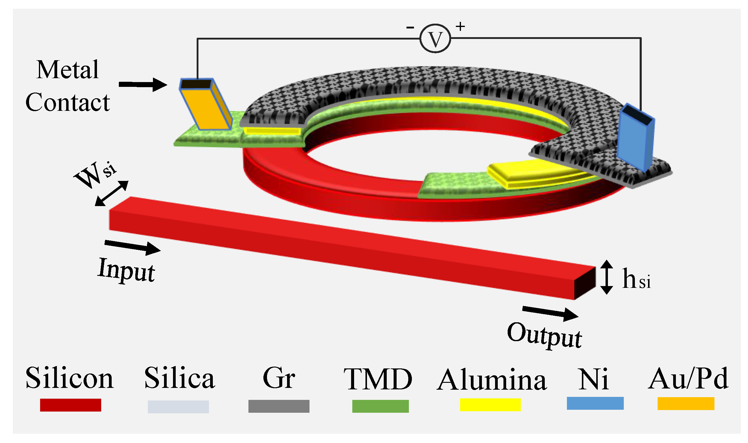
Figure 2.
Ring modulator design showing input/output signals and key system parameters. The dashed area is the portion of the ring covered by the Gr-TMD interface.
Figure 2.
Ring modulator design showing input/output signals and key system parameters. The dashed area is the portion of the ring covered by the Gr-TMD interface.
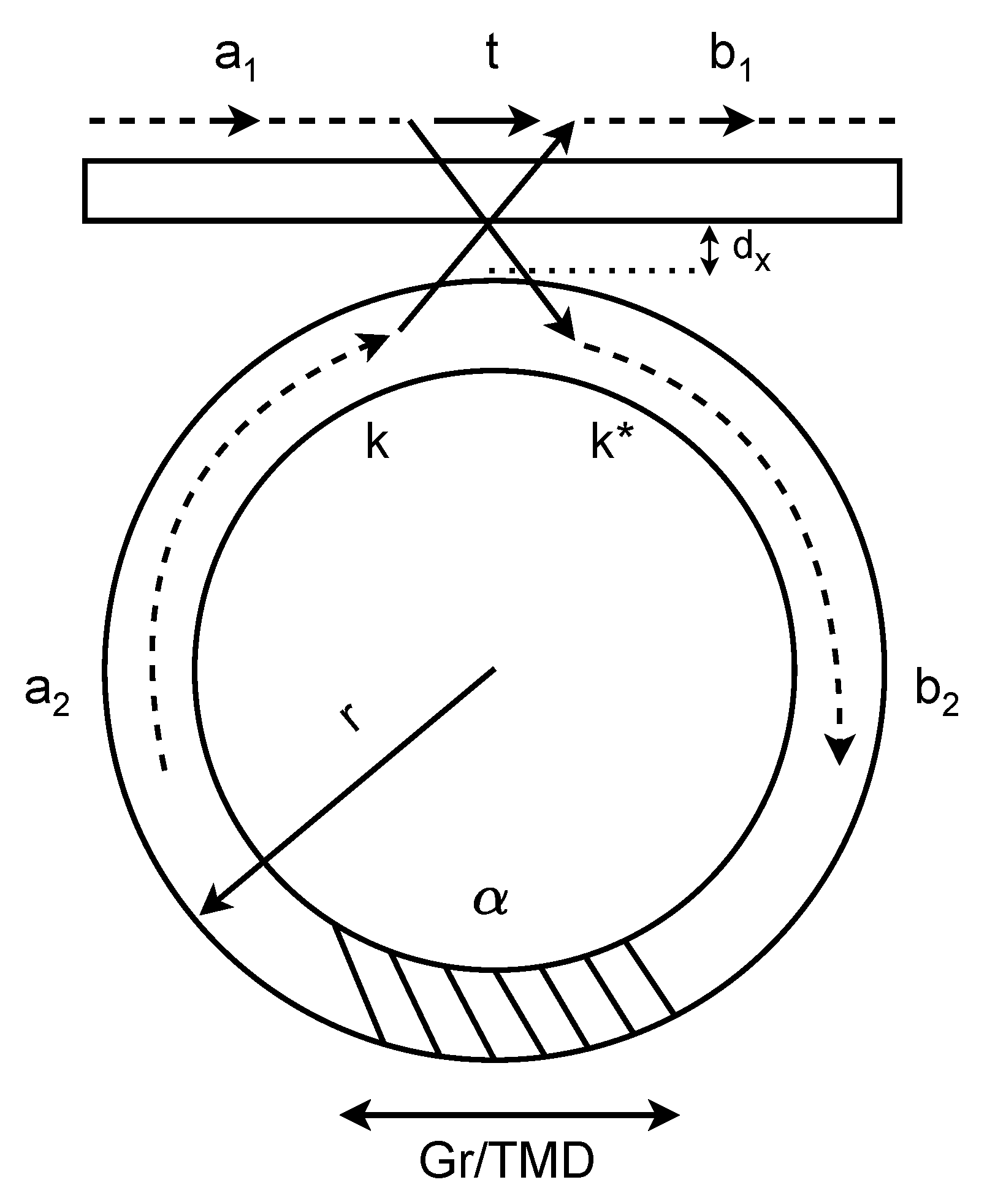
Figure 3.
ON and OFF transmission curves for 25% of ring coverage.
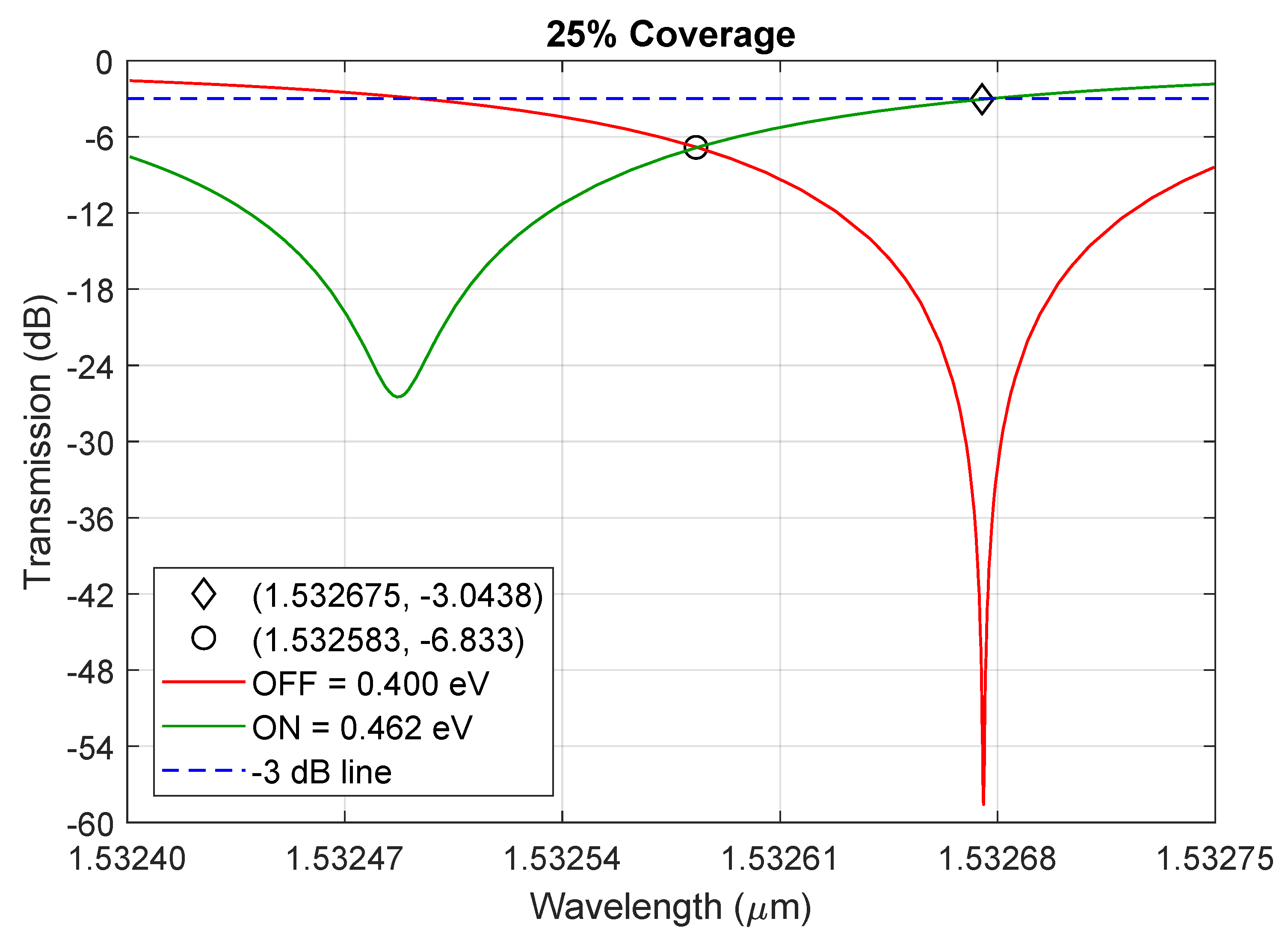
Figure 4.
ON and OFF transmission curves for 55% of ring coverage.
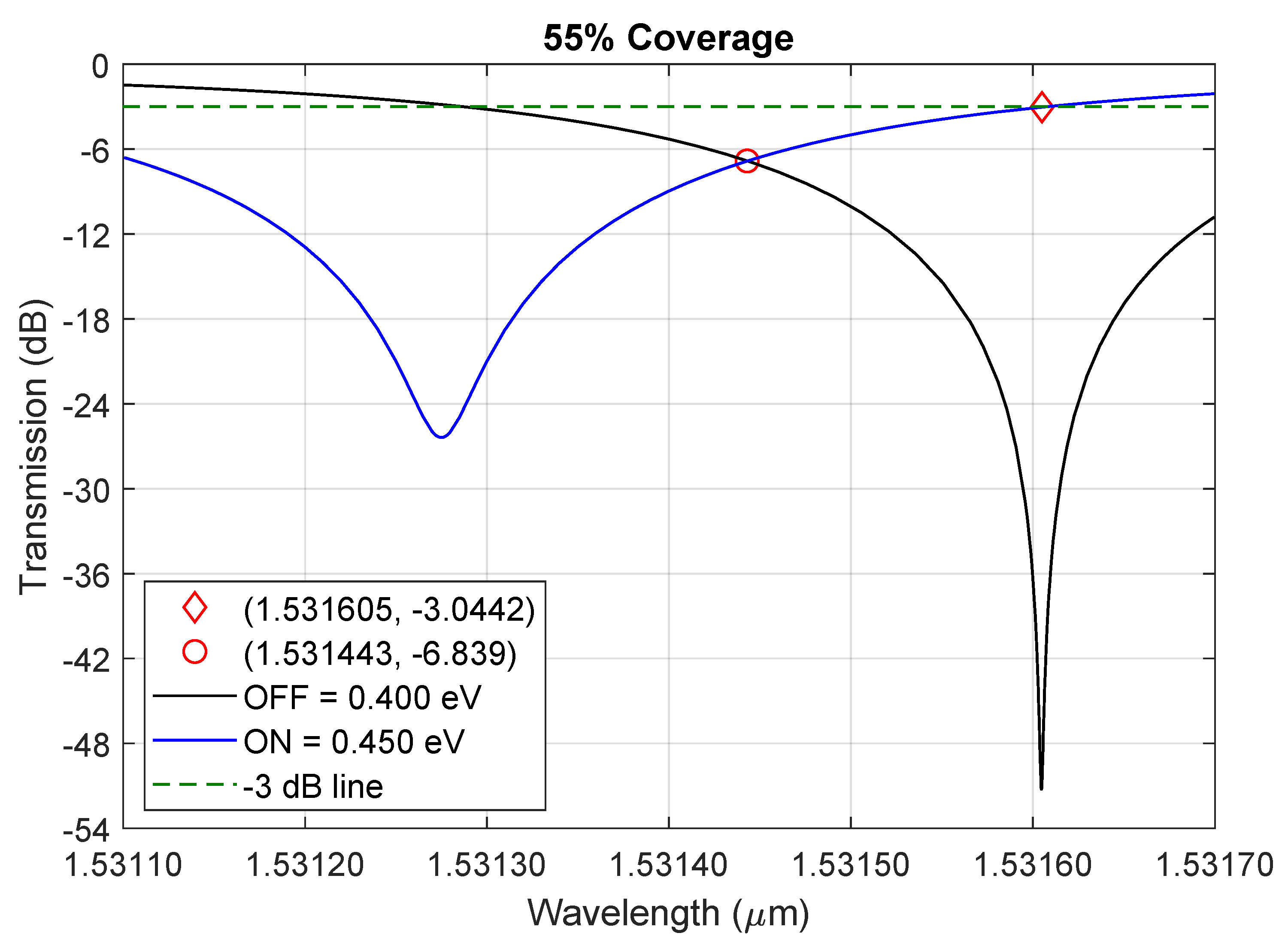
Figure 5.
ON and OFF transmission curves for 85% of ring coverage.
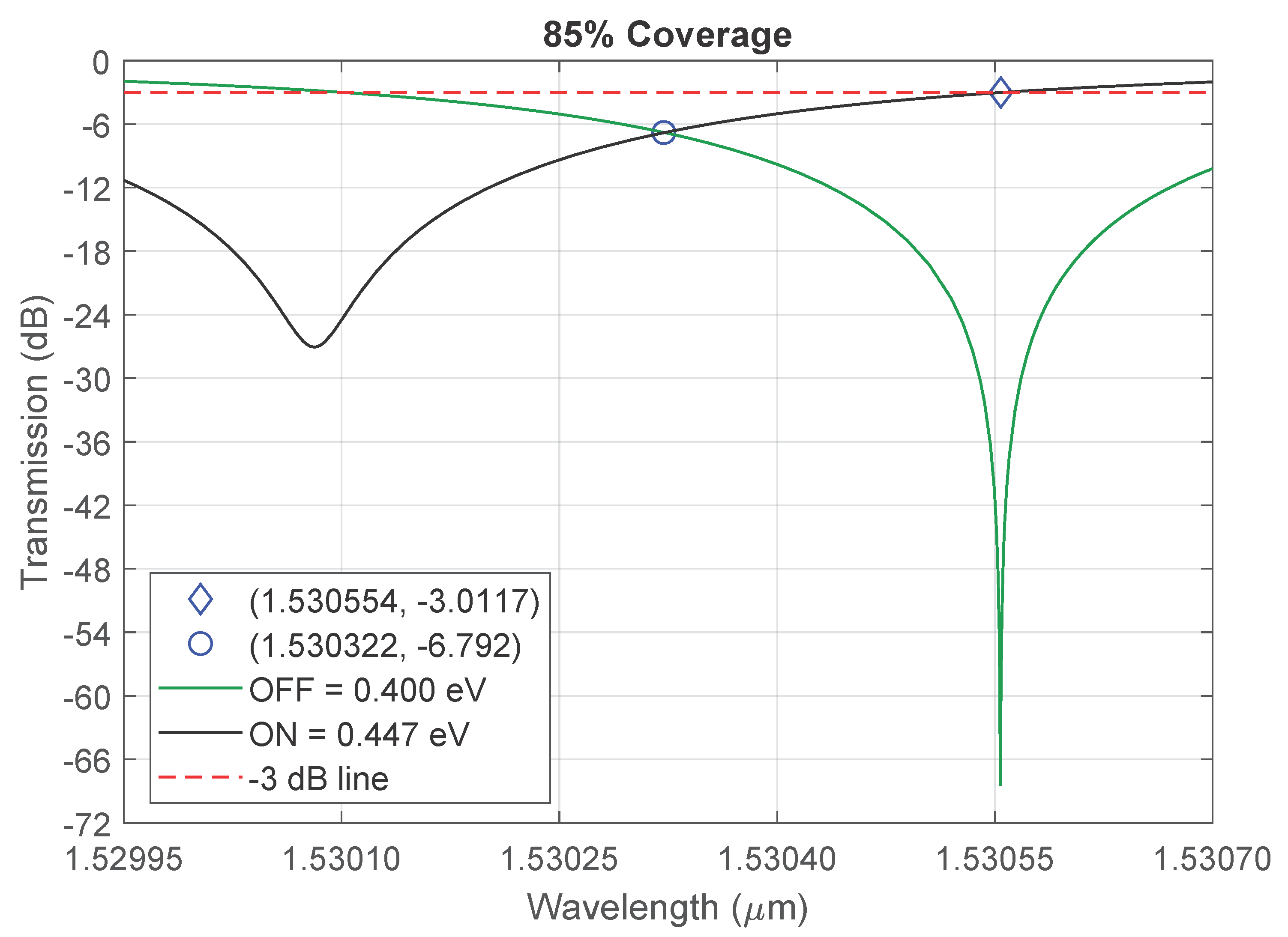
Figure 6.
ON and OFF transmission curves for 100% of ring coverage.
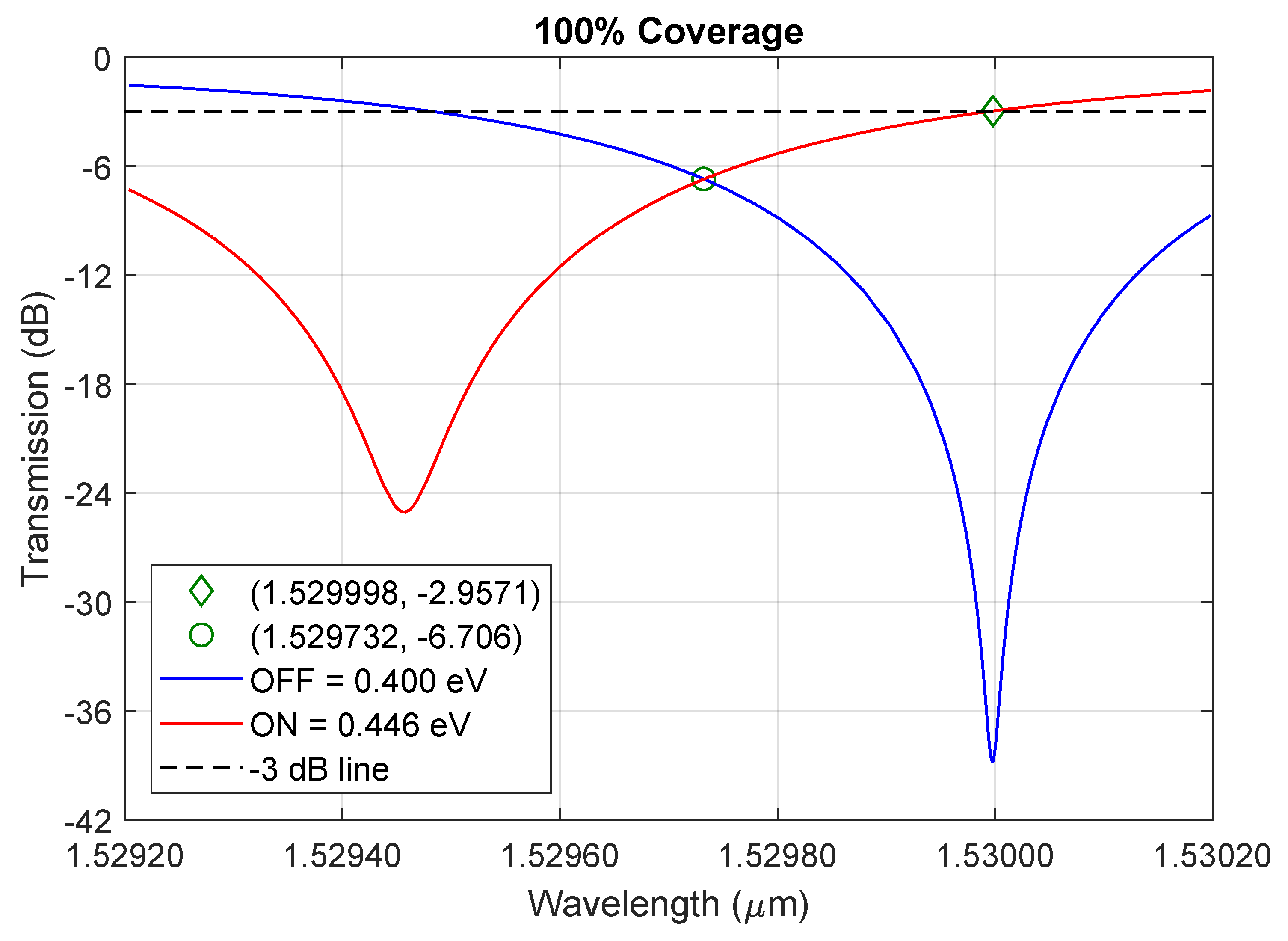
Figure 7.
Chemical potential difference (meV) and resonance shift (nm) when switching between ON/OFF states versus Gr-TMD coverage.
Figure 7.
Chemical potential difference (meV) and resonance shift (nm) when switching between ON/OFF states versus Gr-TMD coverage.
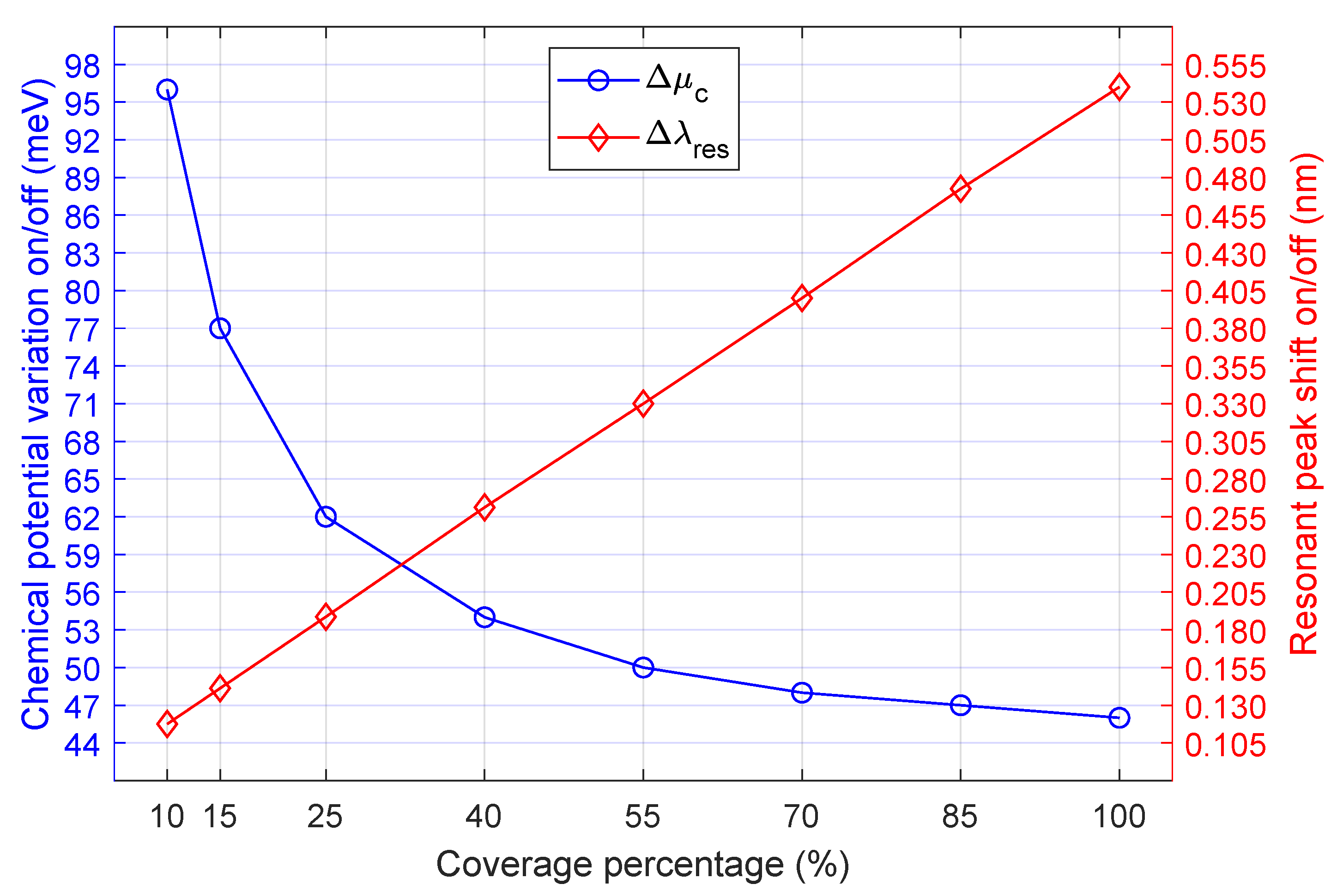
Figure 8.
Variation of the effective index, measured in refractive index units (RIU), in terms of its real and imaginary parts versus chemical potential (eV).
Figure 8.
Variation of the effective index, measured in refractive index units (RIU), in terms of its real and imaginary parts versus chemical potential (eV).
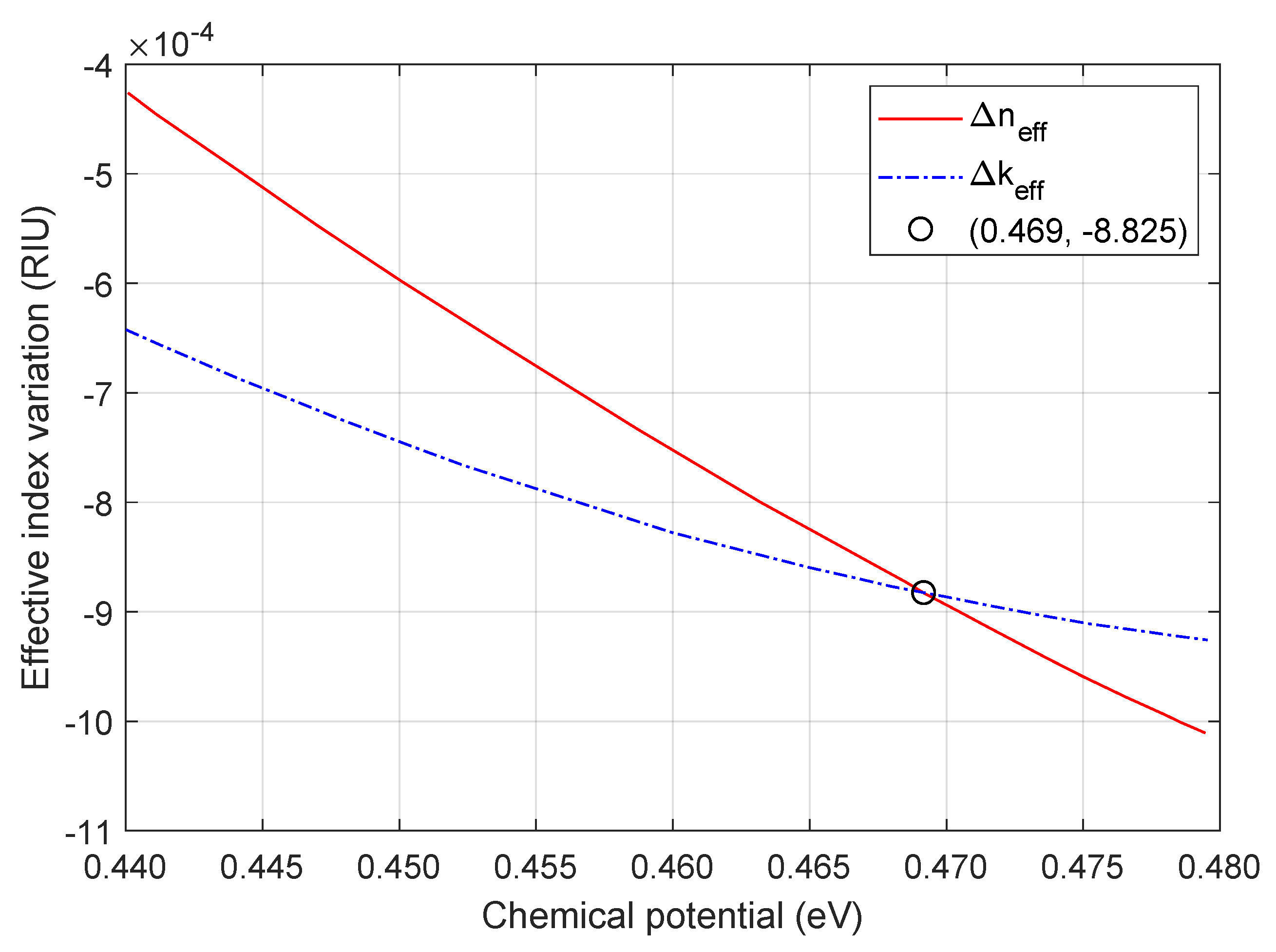
Figure 9.
Modulation efficiency (Vcm) and tuning efficiency (nm/V) versus Gr-TMD coverage.
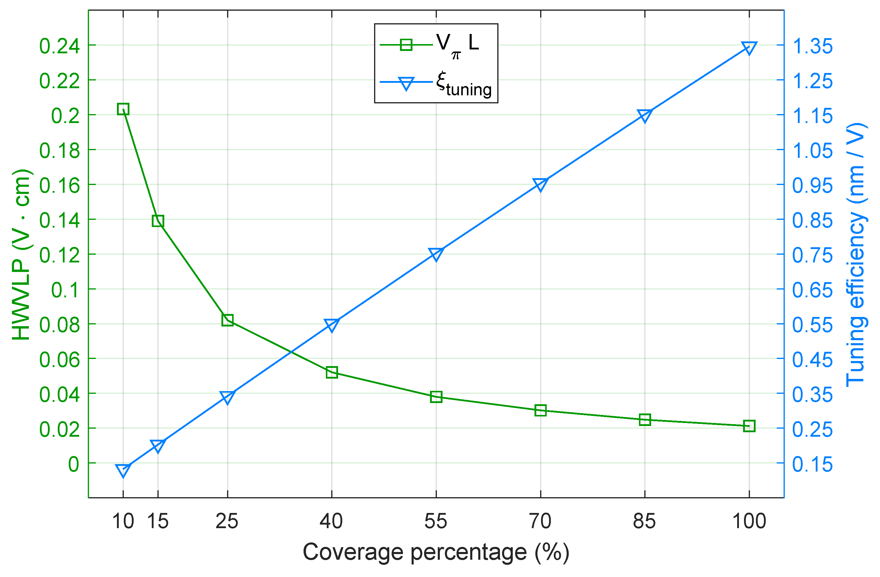
Figure 10.
Modulation bandwidth (GHz) and power consumption (fJ/bit) versus percentage of 2D material coverage.
Figure 10.
Modulation bandwidth (GHz) and power consumption (fJ/bit) versus percentage of 2D material coverage.
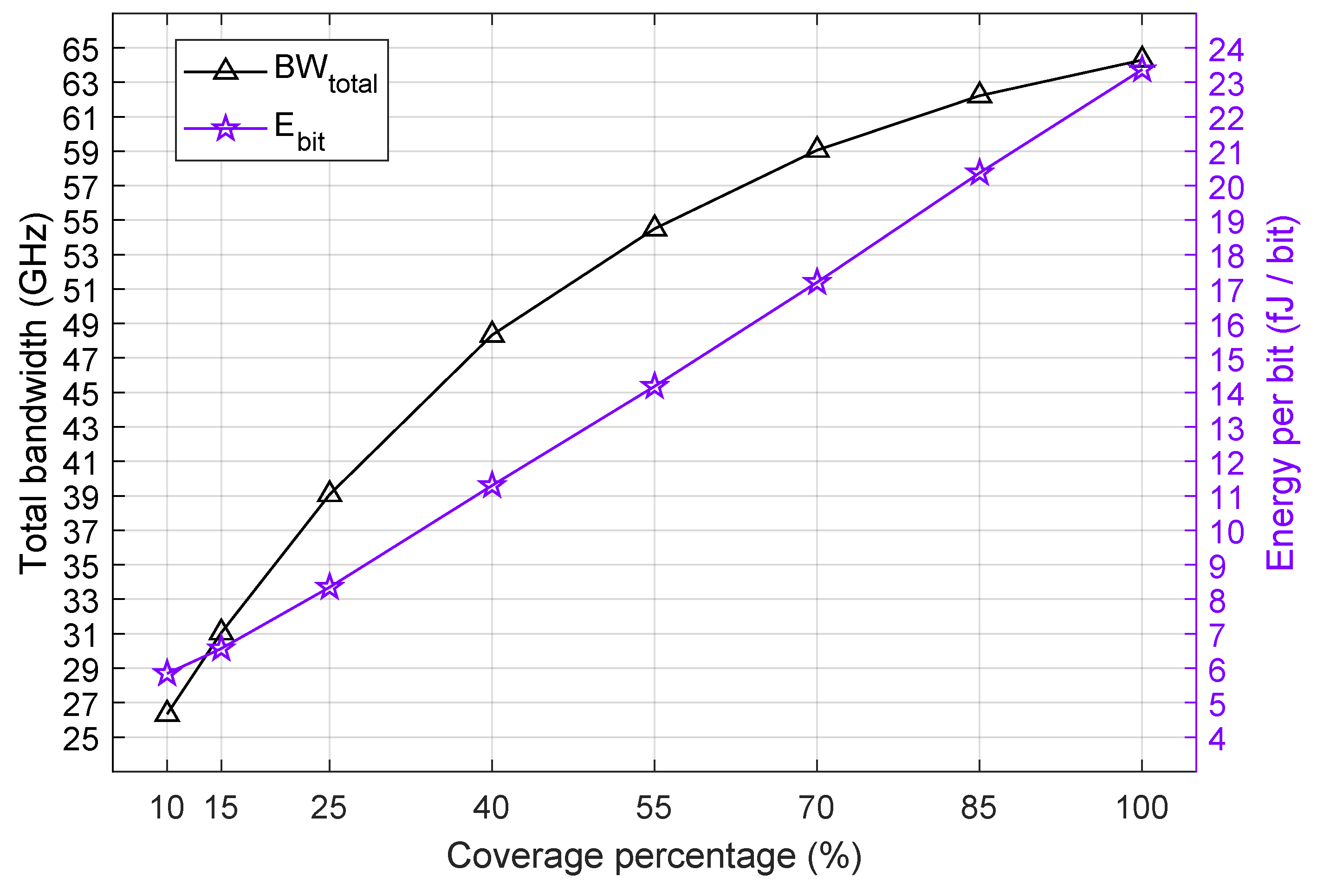
Figure 11.
Modulator’s figure of merit (GHz / (fJ ·)) versus percentage of 2D material coverage.
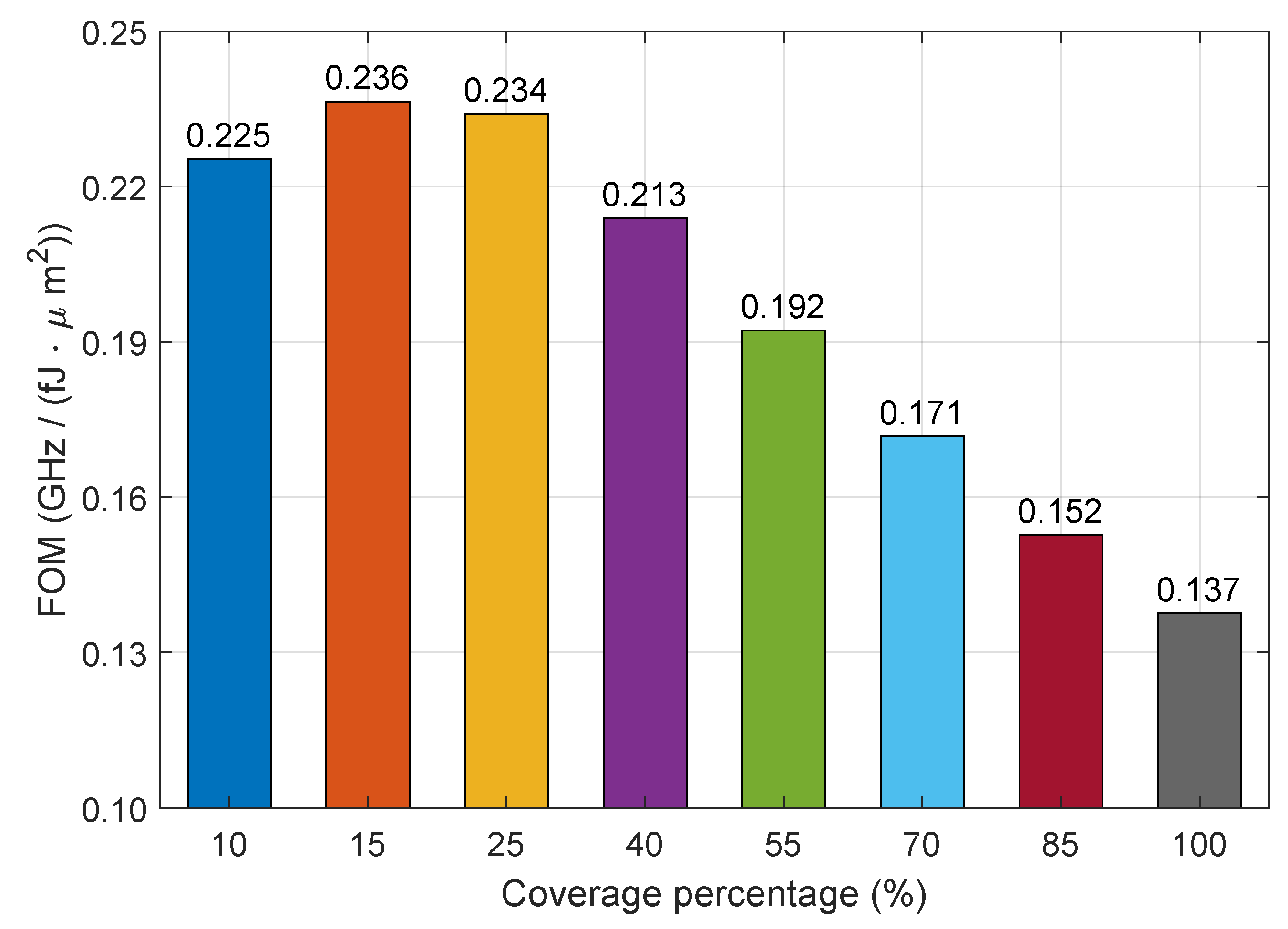

Table 1.
Important Design Parameters.
| (%) | FWHM (GHz) | FSR (nm) | ER (dB) | (nm) | |
|---|---|---|---|---|---|
| 10 | 28.20 | 44.910 | 52.82 | 745 | 0.9923 |
| 15 | 34.25 | 44.900 | 78.05 | 727 | 0.9907 |
| 25 | 46.10 | 44.880 | 55.53 | 700 | 0.9874 |
| 40 | 64.05 | 44.852 | 54.04 | 670 | 0.9826 |
| 55 | 81.01 | 44.824 | 48.19 | 649 | 0.9780 |
| 70 | 98.80 | 44.796 | 45.18 | 632 | 0.9733 |
| 85 | 116.2 | 44.769 | 65.41 | 617 | 0.9686 |
| 100 | 131.6 | 44.740 | 35.83 | 607 | 0.9646 |
Disclaimer/Publisher’s Note: The statements, opinions and data contained in all publications are solely those of the individual author(s) and contributor(s) and not of MDPI and/or the editor(s). MDPI and/or the editor(s) disclaim responsibility for any injury to people or property resulting from any ideas, methods, instructions or products referred to in the content. |
© 2025 by the authors. Licensee MDPI, Basel, Switzerland. This article is an open access article distributed under the terms and conditions of the Creative Commons Attribution (CC BY) license (http://creativecommons.org/licenses/by/4.0/).
Copyright: This open access article is published under a Creative Commons CC BY 4.0 license, which permit the free download, distribution, and reuse, provided that the author and preprint are cited in any reuse.


