
Submitted:
19 November 2025
Posted:
20 November 2025
You are already at the latest version
Abstract
In this study, we explore the integration of a cost-effective triboelectric nanogenerator (TENG) with an large silicon PIN detector(diameter:12mm)for intelligent wireless recognition applications. Wireless communication eliminates the need for physical connections, enabling greater flexibility and scalability in deployment. It allows for seamless integration of AI systems into a wide range of environments without the constraints of wiring, reducing installation complexity and enhancing mobility. Additionally, we demonstrate the TENG's functionality as an autonomous communication unit. The TENG is employed to convert various environmentally triggered signals into digital formats and to autonomously power optoelectronic devices, thus eliminating the need for an external power supply. By integrating optoelectronic components within the self-powered sensing system, the TENG can identify specific trigger information and reduce extraneous noise, thereby improving the accuracy of information transmission.Moreover wireless technology facilitates real-time data transmission and processing. This setup not only enhances the overall efficiency and adaptability of the system but also supports continuous operation in diverse and dynamic settings. This paper introduces a novel CNN-LSTM fusion neural network model. Utilizing the sensing system in combination with the CNN-LSTM neural network enables the collection and identification of variations in the flicker frequency and luminosity of optoelectronic devices. This capability allows for the recognition of environmental trigger signals generated by the TENG. The classification and recognition results of human body trigger signals indicate a recognition accuracy of 92.94%.
Keywords:
triboelectric nanogenerator
; PIN photodetector
; self-powered system
; neural network
1. Introduction
The silicon PIN (Positive-Intrinsic-Negative) detector represents an innovative type of particle-injected semiconductor detector distinguished by a relatively thick depletion layer and a substantial impedance coefficient [1,2,3]. Meanwhile it offers advantages such as simplicity, swift responsiveness, minimal dark current, and high bandwidth [4,5]. These characteristics enable PIN detectors to detect minute changes in photoelectric signals, thereby enhancing the accuracy of signal transmission in self-powered AI intelligent recognition system. Due to its relatively thick barrier layer, it can achieve exceptionally low dark current and high responsiveness. Additionally, due to its large impedance coefficient, it seamlessly interfaces with focal plane array circuits. Moreover Large-area Si-PIN detectors, due to their expansive sensitive surface, can diminish relative measurement discrepancies and heighten measurement sensitivity. In summary, its numerous advantages include high sensitivity, a broad energy range, low noise, linear response, high detection efficiency, stability, and reliability. [6]. These attributes endorse its widespread utilization across diverse domains such as nuclear physics detection, space exploration, environmental monitoring, etc.
As human society advances, the importance of sensors becomes increasingly pronounced [7,8]. These sensors, pivotal in technological evolution, facilitate the simultaneous measurement of various environmental and system parameters, presenting a critical tool for our progressing society [9,10]. Meanwhile the demand for sensor systems in wireless communication and human posture sensing has become increasingly refined. In the field of wireless communication sensing, sensors can utilize short-range communication technologies, such as Bluetooth and ZigBee, to achieve real-time data transmission between devices. Additionally, energy harvesting technologies like TENG enable the creation of self-powered sensor systems, eliminating the reliance on external power sources. In human posture sensing, a combination of sensors such as accelerometers, gyroscopes, and photodetectors can accurately capture human movements and postures, with applications ranging from sports health monitoring to intelligent interactive systems. In industrial production monitoring, a combination of temperature sensors, pressure sensors, and other devices is essential for real-time monitoring of equipment status and the production process [11,12]. Multimodal and multiparameter intelligent sensing fuses data from multiple sources, such as temperature, pressure, and motion, to enable more precise monitoring of both environmental and human conditions. Therefore, silicon PIN sensors empower real-time monitoring of key factors such as temperature, pressure, and humidity, thereby optimizing manufacturing processes, enabling predictive maintenance, and enhancing overall operational efficiency. Additionally, Sensors play a pivotal role in both environmental monitoring and medical fields, aiding in tasks such as environmental parameter assessment [13,14], assisting in disease diagnosis [15], and facilitating personalized medical interventions [16,17,18]. However, with the continuous advancement of technology, the demands for sensor data accuracy and comprehensiveness have increased significantly. Traditional sensor systems, while capable of data collection, frequently encounter limitations in data processing and transmission. To address these challenges, it is essential to develop a self-powered AI intelligent recognition system that offers high detection sensitivity and enables short-range wireless transmission. [19]
A significant challenge with portable silicon PIN detectors lies in their dependence on chemical batteries for power supply. These batteries discharge rapidly, providing limited energy reserves. Concerning the establishment of a mobile monitoring network comprising portable silicon PIN detectors, although individual sensor nodes exhibit modest energy consumption, ensuring the majority of sensor nodes operate normally is pivotal for maintaining the network’s optimal functionality. This presents an energy supply challenge, particularly when involving thousands or more sensor nodes within the network. Therefore, addressing the sustainable energy supply for silicon PIN detectors and further enhancing detection sensitivity and precision to achieve intelligent sensing is also a critical consideration.
TENG has garnered increasing attention as an innovative energy harvesting technology [20,21,22,23,24]. Leveraging its four operational modes, the TENG, facilitated by strategic material selection and structural design, exhibits remarkable adaptability to harness nearly all types of mechanical energy from the surroundings and convert it into electrical energy [25,26,27,28,29,30]. The resultant electrical signals can function as parameters for sensing applications [31,32,33,34,35,36]. With the widespread advancement of TENGs as self-powered active sensors, a diverse array of TENGs with varying operational modes and structures have emerged to monitor an extensive spectrum of parameters. These parameters encompass optoelectronic detection [37,38,39,40], pressure fluctuations [41], vibration [42], displacement [43], object motion tracking [44], and neutron radiation [45]. In prior investigation, we integrated a silicon PIN neutron detector with a TENG to establish self-powered photo detection system [40]. Integrating Silicon PIN detectors and TENGs for self-powered wireless AI intelligent recognition offers several key advantages. Wireless communication eliminates the need for physical connections, enabling greater flexibility and scalability in deployment. It allows for seamless integration of AI systems into a wide range of environments without the constraints of wiring, reducing installation complexity and enhancing mobility. Additionally, wireless technology facilitates real-time data transmission and processing, which is crucial for effective AI-driven recognition and response. This setup not only enhances the overall efficiency and adaptability of the system but also supports continuous operation in diverse and dynamic settings. However, TENG only serves as the power source for PIN detector. Intensive work is need for TENG as sensor for “PIN+TENG” fusion sensing application.
In this paper, a PIN detector is integrated with a triboelectric nanogenerator (TENG) for intelligent environmental trigger signal recognition. We designed and fabricated a large PIN detector (12mm in diameter) with stable electrical characteristics. In our self-powered environmental trigger signal recognition system, we used optoelectronic devices to reduce electrical signal noise and implemented a CNN-LSTM artificial intelligence algorithm for data processing. The TENG senses state actions and generates an electrical signal with motion information to drive LEDs. This status signal is transmitted via the LED to the PIN detector. The output from the PIN detector is then processed by the CNN-LSTM algorithm to extract action perception information. This system can monitor object movements, detect environmental changes, and perform other sensing tasks. Such self-powered sensing systems based on TENG and silicon PIN detectors have significant potential in smart homes, remote monitoring, intelligent robotics, and similar applications for multi-parameter fusion sensing.
2. System Structure Design
The silicon PIN detector comprises a structured arrangement consisting of three layers: a P-type semiconductor layer, an N-type semiconductor layer, and an intrinsic semiconductor layer (a semiconductor devoid of impurities or containing donor and acceptor impurities that exactly compensate each other) sandwiched in between. This design offers notable advantages, including exceptional spatial resolution and heightened sensitivity. The outer layers are significantly doped, whereas the central layer exhibits lighter doping. Upon applying a forward bias voltage, the current is predominantly attributed to the diffusion current of minority carriers, which undergoes exponential growth with increasing forward bias voltage. However, as the voltage escalates, the current assumes a linear relationship with voltage, and the detector assumes the characteristics of a pure resistor. When a reverse bias voltage is imposed upon the PN junction, minority carriers are drawn out by the potent electric field within the space charge region. Subsequently, these removed minority carriers are replenished by internal minority carriers within the semiconductor, leading to the diffusion of electrons and holes under reverse bias voltage. This diffusion current emerges as the primary current in the reverse bias voltage state and remains constant. Typically, the PIN detector operates under negative bias, a configuration dictated by the detector’s intrinsic properties. This reverse-biased setup guarantees a stable current throughout the operational phase.
To address the issue of noise generated during TENG operation, we have developed a straightforward and effective wireless communication approach. Leveraging the high-frequency selectivity of TENG and optical communication technology, this method directly transmits environmental vibrations as digital signals to optoelectronic devices. Through a combination of the silicon PIN detector and CNN-LSTM neural network, changes in brightness and flicker frequency of the Light Emitting Diodes (LEDs) are received and identified. The incorporation of optoelectronic devices in the sensing system aids the TENG in detecting specific trigger information and attenuating extraneous noise, thereby augmenting the selectivity of information transmission. The Schematic diagram of trigger signal detection process is presented in Figure 1(a). Furthermore, optoelectronic devices can function as signal displays, promptly indicating environmental trigger signals generated by the TENG. For instance, when utilized in wearable devices, they can directly indicate the wearer’s current physical activity status. The diagram of the self-powered trigger signal detection system is shown in Figure 1 (b).The operational sequence of the entire system proceeds as follows: the Triboelectric Nanogenerator (TENG) perceives state actions and generates electrical signals, which drive LEDs to produce optical signals. These optical signals are detected by a PIN detector, converting them back into electrical signals. The output from the PIN detector is then processed by a CNN-LSTM algorithm, which analyzes the photoelectric signals to extract action perception information.
Such a system could find applications in monitoring object movements, detecting changes in environmental conditions, or executing other sensing tasks. While achieving wireless monitoring, optical-electronic devices are employed to filter out excess noise. Additionally, these optical-electronic devices can serve as supplementary device drivers, promptly indicating the environmental trigger signals generated by TENG.
3. Device Fabrication
3.1. Fabrication of Silicon PIN Detector
The fabrication process of the silicon PIN detector is illustrated in Figure 2(a). Following a standard semiconductor cleaning process, a high-resistance silicon wafer with a resistivity≥1000Ω/cm and a thickness of 300-400 μm is put into an oxidation furnace. This step generates high-quality silicon dioxide layers of 8000-9000Å on both sides of the silicon wafer. Then, trichloroethylene and oxygen are introduced at a flow ratio of 1:25-1:35 at temperatures ranging from 850 °C to 1150 °C. The chloride ions in the trichloroethylene can combine with positive ions in the silicon wafer, effectively eliminating most of the mobile and fixed ions in the wafer. Following this step, the growth of silicon dioxide continues until the desired thickness is achieved. B+ ions are implanted into the front side of the detector’s detection window to form the p-region and the guard ring. The implantation energy and implantation dose ranges from 35-55 keV and 1×10¹⁴/cm2-5×1014/cm2, respectively. Wet etching process uses TMAH (tetramethylammonium hydroxide). The TMAH concentration used for wet etching ranges from 15-35wt%, and the temperature varies from 65 °C to 95 °C. Following the TMAH etching, P+ ion implantation is performed with an implantation energy ranging from 80-160 keV and an implantation does ranging from 5×10¹⁴/cm2 to 1×10¹⁵/cm2. Lastly, aluminum is sputtered to form the positive electrode and the negative electrode In this study, the silicon PIN detector fabricated by us is depicted in Figure 2(b). The detector has a sensitive area with a diameter of 12mm and a thickness of 100 μm. The I/V characteristics of the silicon PIN detectors were measured using a Keithley 4200 semiconductor parameter analyzer, as shown in Figure 2(c).
3.2. Preparation of TENG
In this study, we employed a contact-separation triboelectric nanogenerator (CS-TENG) fabricated from cardboard to endow the silicon PIN detector with self-powered functionality. The preparation procedure of the CS-TENG can be outlined as follows: Firstly, a piece of cardboard is cut and trimmed to dimensions of 14 cm in length and 7 cm in width, serving as both the supporting and friction layer material. Next, the cardboard is folded, and a piece of polytetrafluoroethylene (PTFE) tape, measuring 6×7 cm2, is affixed and smoothed onto one side of the folded cardboard. This results in two symmetrical regions on the inner side of the cardboard, composed of the PTFE tape and the cardboard. Subsequently, the outer side of the cardboard is processed similarly. Like the inner side, the outer side is divided into two symmetrical regions along the centerline. Two pieces of copper foil, each measuring 6×7 cm2, are uniformly applied to these two distinct regions. These copper foils function as the conductive layers for the external circuit. Additionally, wires are connected to the copper foils to establish links with the external detection circuit. Its detailed preparation process is shown in Figure 3(a).
The CS-TENG operates on the principle of harnessing charge flow generated through frictional interactions between the cardboard and polytetrafluoroethylene (PTFE) tape. In this configuration, the PTFE tape and cardboard serve as the lower and upper friction layers, respectively, while two copper foils are integrated as the conductive electrodes. When these dissimilar material layers come into contact and then separate, they induce disparate charges on their respective surfaces. Subsequently, as the two frictional layers are separated, the electrostatic induction effect induces a charge on the copper foils, leading to the establishment of an electric potential difference. This potential difference drives the movement of electrons, causing them to flow from the upper copper foil to the lower copper foil, as visually depicted in Figure 3(b). Further, we used COMSOL Multiphysics software to simulate the TENG power generation process, and the simulation results are shown in Figure 3(c). As can be seen, with cardboard and PTFE The distance between the friction layers increases from 1 mm to 3 mm, and the potential difference between the two friction layers gradually increases.
Furthermore, we tested and analyzed the output signals of the CS-TENG. The maximum output voltage and current achieved by the CS-TENG used in this study can reach up to 480 V and 26.18μA respectively., as illustrated in Figure 4(a) and Figure 4(b). From Figure 4(c), it can be observed that the internal resistance of the proposed CS-TENG approximately equals 3 MΩ, with a Maximum power density of 311.11 μW/cm2. In addition, its corresponding load current characteristics are shown in Figure 4(d).
4. Triggered Signals Recognition Based on Self-Powered Sensing System and Neural Network
4.1. The Self-Powered Sensing System Based on TENG and Silicon PIN Detector
The schematic diagram of the human trigger signal recognition process is shown in Figure 5. In this study, we have devised an innovative sensing system that harnesses the resonance phenomenon of the TENG alongside optical communication technology. Through the exploitation of TENG’s high-frequency selectivity and optical communication technology, we have established a straightforward yet efficient approach for directly transmitting environmental vibrations as digital signals to the receiver. In this system, we employ a CS-TENG to process information and act as the power source for the real-time transmission of collected data. The CS-TENG converts a sequence of environmental trigger signals into digital data and propels electronic optical devices for the instantaneous transmission of digital information, all without necessitating an external power source.
The sensing system established in this research is depicted in Figure 6, encompassing two distinct communication units: the perception unit and the recognition unit. The perception unit employs the CS-TENG to supply power to an LED device, with a rectifier bridge linking the CS-TENG and the light-emitting device (LED). In response to different environmental trigger signals, the LED exhibits varying brightness and flicker frequency. However, when the differences in environmental trigger signals are subtle, the changes in LED brightness and flicker frequency are also minimal, rendering them challenging to identify directly through visual or image recognition techniques. Consequently, in this study, we employ a silicon PIN detector to discern the fluctuations in LED brightness and flicker frequency. Capitalizing on its outstanding photosensitivity characteristics, the silicon PIN detector can accurately detect even the most subtle variations in LED brightness and flicker frequency. This capability facilitates the recognition of environmental trigger signals, aided by neural network algorithms. The recognition unit utilizes a constant voltage source to energize the silicon PIN detector, incorporating a relatively high load in the circuit. This configuration enables precise measurement of voltage variations across the terminals of the silicon PIN detector.
4.2. Neural Network Model
The collected triggering signal in this investigation represents a temporal phenomenon distinguished by both spatiotemporal correlation and instability. Convolutional Neural Networks (CNNs) are adept at discerning the spatial characteristics within the signal, whereas Long Short-Term Memory networks (LSTMs) excel at isolating the temporal correlation features. Based on this, a novel hybrid deep neural network model, integrating CNN and LSTM architectures, is proposed herein for the purpose of classifying human triggering signals into four distinct categories. The network architecture of the CNN-LSTM fusion model is shown in Figure 7.
In detail, the CNN component of the model comprises two convolutional layers paired with a maximum pooling layer, responsible for extracting spatial features from the input human triggering signal. Following the CNN stage, which completes the extraction of features from the human body triggering signal, the high-dimensional spatial features are segmented into sequences based on time and sequentially inputted into the LSTM network for training to discern temporal relationships between features. The LSTM layer is capable of learning the timing of input signals across the temporal dimension, thereby facilitating the acquisition of temporal correlation features, which enables the network to better comprehend the inherent time-series relationships among features during different intervals. A Dropout layer, integrated after the LSTM layer, is introduced to randomly discard segments of the network with a specified probability, aiming to mitigate overfitting and enhance the model’s generalization capacity. Ultimately, the information derived from both the convolutional and LSTM layers is consolidated and outputted through the fully connected layer, employing the Softmax activation function. The specific hyperparameter configurations of the CNN-LSTM model are detailed in Table 1.
5. Experiment and Result Analysis
5.1. Experimental Data Collection
The volunteers’ different triggering actions directly act on the CS-TENG. The electrical signal generated by the CS-TENG supplies energy to the LED after passing through the rectifier bridge circuit, causing the LED to show different flicker frequencies and brightness. In a dark and shading environment, silicon PIN photodetectors with high sensitivity to light sources can clearly capture subtle changes in LED light and produce corresponding voltage changes, thereby capturing the light signals generated by volunteers’ different triggering actions. The schematic diagram of data collection process is illustrated in Figure 8.
The silicon PIN photodetector is connected externally to a 6V constant voltage source and a 2MΩ load. Voltage across the silicon PIN photodetector is measured using a Keithley 6514 system electrometer. Each action performed by a volunteer lasts for 40 s. To ensure data reliability, voltage change data during the mid-20-s interval is selected as the dataset, comprising a time series consisting of 20 s and 154 data points. This study gathers a total of 5100 sets (5100*154) of voltage change data from both ends of the silicon PIN photodetector, constituting the trigger actions of palm (M), knee (E), elbow (W), and plantar (R). Specifically, there are 1200 sets of M-class data, 1200 sets of E-class data, 1500 sets of W-class data, and 1200 sets of R-class data.
5.2. Data Processing
To enhance model stability and mitigate the risk of overfitting, thereby improving its generalization across diverse datasets, the experiment employed the Z-score normalization method. This method ensures that the processed dataset exhibits a zero mean and unit variance, conforming to the standard normal distribution. Subsequently, Min-Max scaling normalization was applied to scale the data range between 0 and 1, preserving the original scale relationships and structural characteristics of the data.
5.3. Analysis of Results
Throughout the training process, 60% of the time series data was allocated for training, 20% for validation, and another 20% for testing purposes. The model underwent 200 training iterations, with initial learning rate and L2 regularization parameters set to 0.001 and 0.0001, respectively. Employing the Adam gradient descent algorithm optimized the network’s structural performance. Additionally, a learning rate decay strategy was implemented, wherein the learning rate decreased by 0.1 after 120 iterations. Figure 9(a)(b) illustrates the accuracy and loss rate curves observed during the training phase. The CNN-LSTM model achieved accuracy rates of 96.37% and 92.64% on the training and validation sets, respectively.
To further validate the classification performance of the CNN-LSTM model, this study conducts a comparative analysis with existing CNN and LSTM algorithms. The CNN algorithm comprises two one-dimensional convolutional blocks followed by a fully connected layer, while the LSTM algorithm consists of two LSTM blocks, two dropout layers, and a fully connected layer. Hyperparameter settings are dynamically adjusted to optimize accuracy. Table 2 presents the macro-average and accuracy performance metrics, including precision, recall, and F1 scores, evaluated on the test set.
Table 2 reveals that the CNN-LSTM model achieves the highest average accuracy, with its accuracy on the test set reaching 92.94%, surpassing the 87.94% achieved by the CNN model and the 87.64% achieved by the LSTM model. Precision and recall metrics for the CNN model are comparable, with the F1 score closely aligned with both. While the LSTM model exhibits slightly lower precision but slightly higher recall, resulting in a marginally lower F1 score compared to the CNN model, it still demonstrates a relatively balanced precision-recall trade-off. The superior performance of the CNN-LSTM model across all metrics can be attributed to its integration of advantages from both network architectures, enabling feature extraction at various levels.
As depicted in Table 3, the CNN-LSTM model exhibits notably higher accuracy and recall rates for samples belonging to the E and W classes compared to both the CNN and LSTM models. This observation underscores the robust anti-interference capabilities of the CNN-LSTM model. Moreover, the CNN-LSTM model demonstrates superior overall classification performance on the test set, indicating its suitability for addressing complex real-world challenges. This suggests that the CNN-LSTM model proposed in this study presents an optimal solution for such scenarios.
6. Conclusion
This paper introduces a self-powered sensing system consisting of two distinct communication units. These units operate by harnessing specific-frequency environmental trigger signals as their energy source. The collected trigger signals are converted into digital signals and can be directly transmitted using electro-optical devices, eliminating the need for external power sources. The versatility of TENG technology allows for the transmission of trigger signals at various frequencies. Utilizing the CNN-LSTM neural network model proposed within this study for the identification of four distinct TENG trigger signals, the system attains precise recognition of environmental trigger signals, achieving a success rate of up to 92.94%. It is noted that this self-powered sensing systems can be extended to other types of self-powered sensors. By incorporating different sensing elements and signal processing methods in the sensor design, it is possible to achieve multifunctional sensing, thereby meeting the requirements of different application scenarios. This work has made significant contributions to the development of self-powered systems and has laid a solid foundation for establishing future self-powered sensing networks.
Acknowledgments
This work is supported by Opening Fund of State Key Laboratory of Fire Science (SKLFS) under Grant No. HZ2024-KF04, and the New Chongqing Youth Innovation Talent Project (CSTB2024NSCQ - QCXMX0072), Beibei District scientific research project (2025zzcxyj-07), the Science and Technology Research Program of Chongqing Municipal Education Commission (Grant No. KJZD-K202500202), and Open Fund of Key Laboratory for Information Science of Electromagnetic Waves, Fudan University (Grant No. EMW202405).
References
- Zhu Z, Pu M, Jiang M; et al. Bonding Processing and 3D Integration of High-Performance Silicon PIN Detector for ΔE-E telescope[J]. Processes 2023, 11, 627. [Google Scholar] [CrossRef]
- Yu B, Zhao K, Yang T; et al. Process effects on leakage current of Si-PIN neutron detectors with porous microstructure[J]. physica status solidi (a) 2017, 214, 1600900. [Google Scholar] [CrossRef]
- Li H X, Li Z K, Wang F C; et al. Application of stratified implantation for silicon micro-strip detectors[J]. Chinese Physics C 2015, 39, 066005. [Google Scholar] [CrossRef]
- Geis M W, Spector S J, Grein M E; et al. CMOS-compatible all-Si high-speed waveguide photodiodes with high responsivity in near-infrared communication band[J]. IEEE Photonics Technology Letters 2007, 19, 152–154. [Google Scholar] [CrossRef]
- Oehme M, Werner J, Kasper E; et al. High bandwidth Ge pin photodetector integrated on Si[J]. Applied physics letters.
- Abdel N S, Pallon J, Ros L; et al. Characterizations of new ΔE detectors for single-ion hit facility[J]. Nuclear Instruments and Methods in Physics Research Section B: Beam Interactions with Materials and Atoms 2014, 318, 281–286. [Google Scholar] [CrossRef]
- Gravina R, Alinia P, Ghasemzadeh H; et al. Multi-sensor fusion in body sensor networks: State-of-the-art and research challenges[J]. Information Fusion 2017, 35, 68–80. [Google Scholar] [CrossRef]
- Geng H, Wang Z, Chen Y; et al. Multi-sensor filtering fusion with parametric uncertainties and measurement censoring: Monotonicity and boundedness[J]. IEEE Transactions on Signal Processing 2021, 69: 5875-5890.
- Wang Y, Li J, Viehland D. Magnetoelectrics for magnetic sensor applications: Status, challenges and perspectives[J]. Materials Today 2014, 17, 269–275.
- Mittal A, Davis L S. A general method for sensor planning in multi-sensor systems: Extension to random occlusion[J]. International journal of computer vision 2008, 76, 31–52. [Google Scholar]
- Chen, W. Intelligent manufacturing production line data monitoring system for industrial internet of things[J]. Computer communications 2020, 151, 31–41. [Google Scholar] [CrossRef]
- Bal, M. An industrial Wireless Sensor Networks framework for production monitoring. In Proceedings of the 2014 IEEE 23rd International Symposium on Industrial Electronics (ISIE), Istanbul, Turkey, 1–4 June 2014; pp. 1442–1447. [Google Scholar]
- Hayat H, Griffiths T, Brennan D; et al. The state-of-the-art of sensors and environmental monitoring technologies in buildings[J]. Sensors 2019, 19, 3648. [Google Scholar] [CrossRef]
- Mois G, Folea S, Sanislav T. Analysis of three IoT-based wireless sensors for environmental monitoring[J]. IEEE Transactions on Instrumentation and Measurement 2017, 66, 2056–2064. [Google Scholar] [CrossRef]
- Zhang L, Khan K, Zou J; et al. Recent advances in emerging 2D material-based gas sensors: Potential in disease diagnosis[J]. Advanced Materials Interfaces 2019, 6, 1901329. [Google Scholar] [CrossRef]
- Tyler J, Choi S W, Tewari M. Real-time, personalized medicine through wearable sensors and dynamic predictive modeling: A new paradigm for clinical medicine[J]. Current opinion in systems biology 2020, 20, 17–25. [Google Scholar] [CrossRef] [PubMed]
- Andreu-Perez J, Leff D R, Ip H M D; et al. From wearable sensors to smart implants-–toward pervasive and personalized healthcare[J]. IEEE Transactions on Biomedical Engineering 2015, 62, 2750–2762. [Google Scholar] [CrossRef]
- Wang Z, Xiong H, Zhang J; et al. From personalized medicine to population health: A survey of mHealth sensing techniques[J]. IEEE Internet of Things Journal 2022, 9, 15413–15434. [Google Scholar] [CrossRef]
- Zhu M, Yi Z, Yang B; et al. Making use of nanoenergy from human–Nanogenerator and self-powered sensor enabled sustainable wireless IoT sensory systems[J]. Nano Today, 1010.
- Zhang H, Wang J, Xie Y; et al. Self-powered, wireless, remote meteorologic monitoring based on triboelectric nanogenerator operated by scavenging wind energy[J]. ACS applied materials & interfaces 2016, 8, 32649–32654. [Google Scholar]
- Song W, Gan B, Jiang T; et al. Nanopillar arrayed triboelectric nanogenerator as a self-powered sensitive sensor for a sleep monitoring system[J]. Acs Nano 2016, 10, 8097–8103. [Google Scholar] [CrossRef] [PubMed]
- Gao H, Hu M, Ding J; et al. Investigation of contact electrification between 2D MXenes and MoS2 through density functional theory and triboelectric probes[J]. Advanced Functional Materials 2023, 33, 2213410. [Google Scholar] [CrossRef]
- Zhang J, Xu Q, Li H; et al. Self-powered electrodeposition system for Sub-10-Nm silver nanoparticles with high-efficiency antibacterial activity[J]. The Journal of Physical Chemistry Letters 2022, 13, 6721–6730. [Google Scholar] [CrossRef] [PubMed]
- Guo X, He J, Zheng Y; et al. High-performance triboelectric nanogenerator based on theoretical analysis and ferroelectric nanocomposites and its high-voltage applications[J]. Nano Research Energy 2023, 2, e9120074. [Google Scholar] [CrossRef]
- Lin, Long, Wang; et al. A Hybridized Power Panel to Simultaneously Generate Electricity from Sunlight, Raindrops, and Wind around the Clock[J]. Advanced Energy Materials.
- Li X, Luo J, Han K; et al. Stimulation of ambient energy generated electric field on crop plant growth[J]. Nature Food.
- Ren Z, Y Ding, Nie J; et al. Environmental Energy Harvesting Adapting to Different Weather Conditions and Self-Powered Vapor Sensor Based on Humidity-Responsive Triboelectric Nanogenerators[J]. ACS Applied Materials & Interfaces.
- Lin H, He M, Jing Q; et al. Angle-shaped triboelectric nanogenerator for harvesting environmental wind energy[J]. Nano Energy 2019, 56, 269–276. [Google Scholar] [CrossRef]
- Feng Y, Zhang L, Zheng Y; et al. Leaves based triboelectric nanogenerator (TENG) and TENG tree for wind energy harvesting[J]. Nano Energy 2019, 55, 260–268. [Google Scholar] [CrossRef]
- Kim J, Ryu H, Lee J H; et al. Triboelectric Nanogenerators: High Permittivity CaCu3Ti4O12 Particle-Induced Internal Polarization Amplification for High Performance Triboelectric Nanogenerators (Adv. Energy Mater. 9/2020)[J]. Advanced Energy Materials 2020, 10, 2070040.
- Lin Z H, Cheng G, Lin L; et al. Water–solid surface contact electrification and its use for harvesting liquid-wave energy[J]. Angewandte Chemie International Edition 2013, 52, 12545–12549. [Google Scholar] [CrossRef]
- Zhu G, Su Y, Bai P; et al. Harvesting water wave energy by asymmetric screening of electrostatic charges on a nanostructured hydrophobic thin-film surface[J]. ACS nano 2014, 8, 6031–6037. [Google Scholar] [CrossRef] [PubMed]
- Chen J, Yang J, Li Z; et al. Networks of triboelectric nanogenerators for harvesting water wave energy: A potential approach toward blue energy[J]. ACS nano 2015, 9, 3324–3331. [Google Scholar] [CrossRef]
- Ren Z, Zheng Q, Wang H; et al. Wearable and Self-Cleaning Hybrid Energy Harvesting System based on Micro/Nanostructured Haze Film[J]. Nano Energy 2019, 67, 104243. [Google Scholar]
- Zheng Y, Liu T, Wu J; et al. Energy conversion analysis of multilayered triboelectric nanogenerators for synergistic rain and solar energy harvesting[J]. Advanced Materials 2022, 34, 2202238. [Google Scholar] [CrossRef]
- Xu Q, Fang Y, Jing Q; et al. A portable triboelectric spirometer for wireless pulmonary function monitoring[J]. Biosensors and Bioelectronics 2021, 187, 113329. [Google Scholar]
- Zheng Y, Cheng L, Yuan M, Wang Z, Zhang L, Qin Y* and Jing T. An electrospun nanowire-based triboelectric nanogenerator and its application in a fully self-powered UV detector. Nanoscale 2014, 6, 7842–7846. [Google Scholar] [CrossRef]
- Gang Cheng, Haiwu Zheng, Feng Yang, Lei Zhao, Mingli Zheng, Junjie Yang, Huaifang Qin, Zuliang Du*, ZhongLin Wang*. Managing and maximizing the output power of atriboelectric nanogenerator by controlled tip–electrode air-discharging and application for UV sensing. Nano Energy 2018, 44, 208–216. [Google Scholar] [CrossRef]
- Han Lei, Peng Mingfa, Wen Zen, Liu Yina, Zhang Yi, Zhu Qianqian, Lei Hao, Liu Sainan, Zheng Li*, Sun Xuhui*, Li Hexing*. Self-driven photodetection based on impedance matching effect between a triboelectric nanogenerator and a MoS2 nanosheets photodetector. Nano Energy 2019, 59, 592–599. [Google Scholar]
- Wang J, Xia K, Li T; et al. Self-powered silicon PIN photoelectric detection system based on triboelectric nanogenerator[J]. Nano Energy 2020, 69, 104461. [Google Scholar] [CrossRef]
- Wang Z, Bu T, Li Y; et al. Multidimensional force sensors based on triboelectric nanogenerators for electronic skin [J]. ACS Applied Materials & Interfaces 2021, 13, 56320–56328. [Google Scholar]
- Li S, Liu D, Zhao Z; et al. A fully self-powered vibration monitoring system driven by dual-mode triboelectric nanogenerators [J]. ACS Nano 2020, 14, 2475–2482. [Google Scholar] [CrossRef] [PubMed]
- Li C, Wang Z, Shu S; et al. A self-powered vector angle/displacement sensor based on triboelectric nanogenerator [J]. Micromachines 2021, 12, 231–240. [Google Scholar] [CrossRef] [PubMed]
- Zeng Y, Xiang H, Zheng N; et al. Flexible triboelectric nanogenerator for human motion tracking and gesture recognition [J]. Nano Energy, 1066.
- Zhu Z, Li B, Zhao E; et al. Self-powered silicon PIN neutron detector based on triboelectric nanogenerator[J]. Nano Energy, 1076.
Figure 1.
(a) Schematic diagram of trigger signal detection process (b) Diagram of the trigger signal detection system.
Figure 1.
(a) Schematic diagram of trigger signal detection process (b) Diagram of the trigger signal detection system.
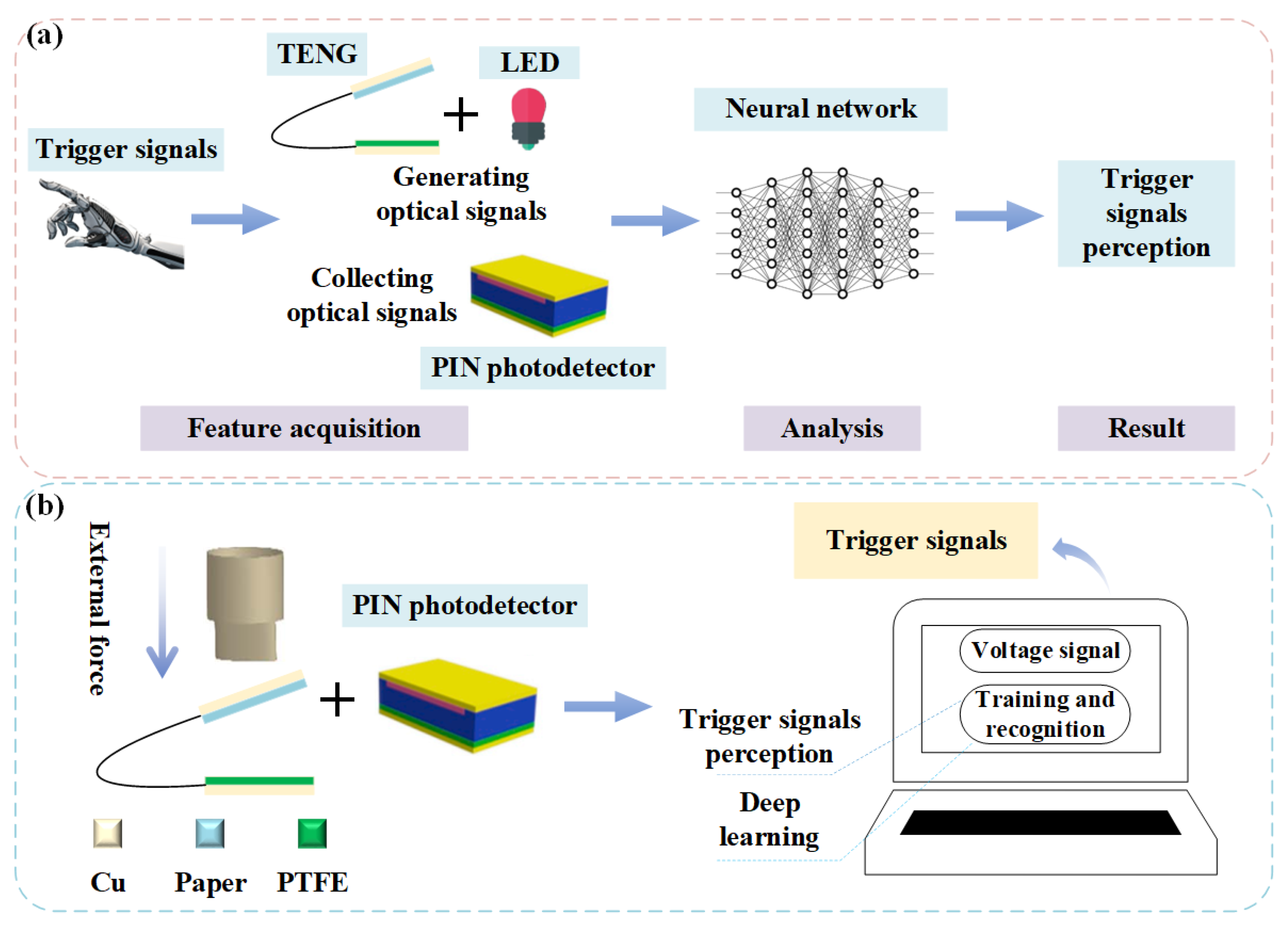
Figure 2.
(a) Fabrication Process of Silicon PIN Detector (b) Images of Silicon PIN Detector (c)I/V Characteristics of Silicon PIN Detector.
Figure 2.
(a) Fabrication Process of Silicon PIN Detector (b) Images of Silicon PIN Detector (c)I/V Characteristics of Silicon PIN Detector.
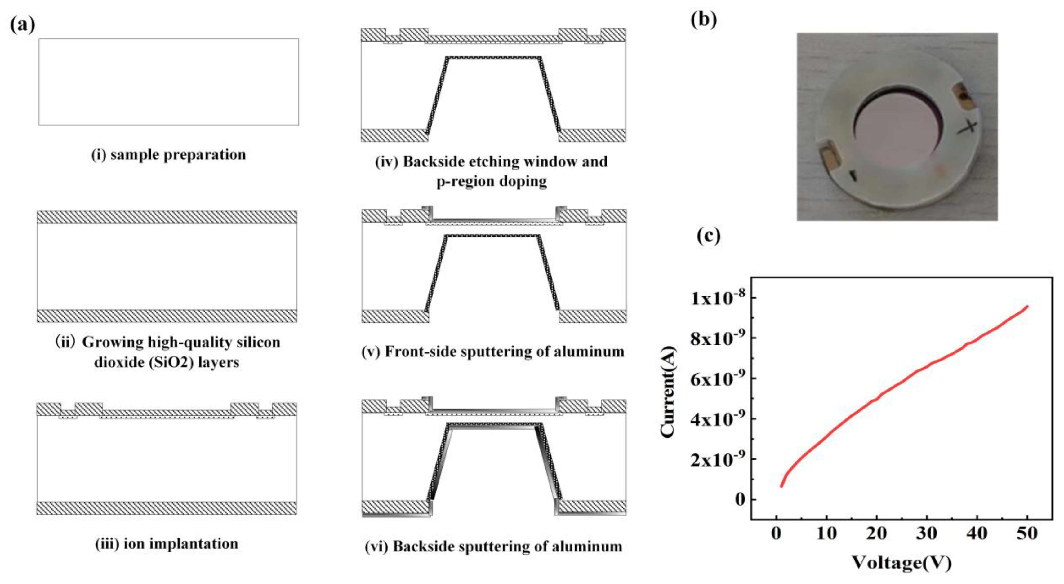
Figure 3.
(a) Fabrication Process of TENG (b) Principle of TENG (c) COMSOL simulation potential diagram: (i) d=1mm, (ii) d=2mm, (iii) d=3mm (top layer is Paper and bottom layer is PTFE; d is the distance between the two layers).
Figure 3.
(a) Fabrication Process of TENG (b) Principle of TENG (c) COMSOL simulation potential diagram: (i) d=1mm, (ii) d=2mm, (iii) d=3mm (top layer is Paper and bottom layer is PTFE; d is the distance between the two layers).
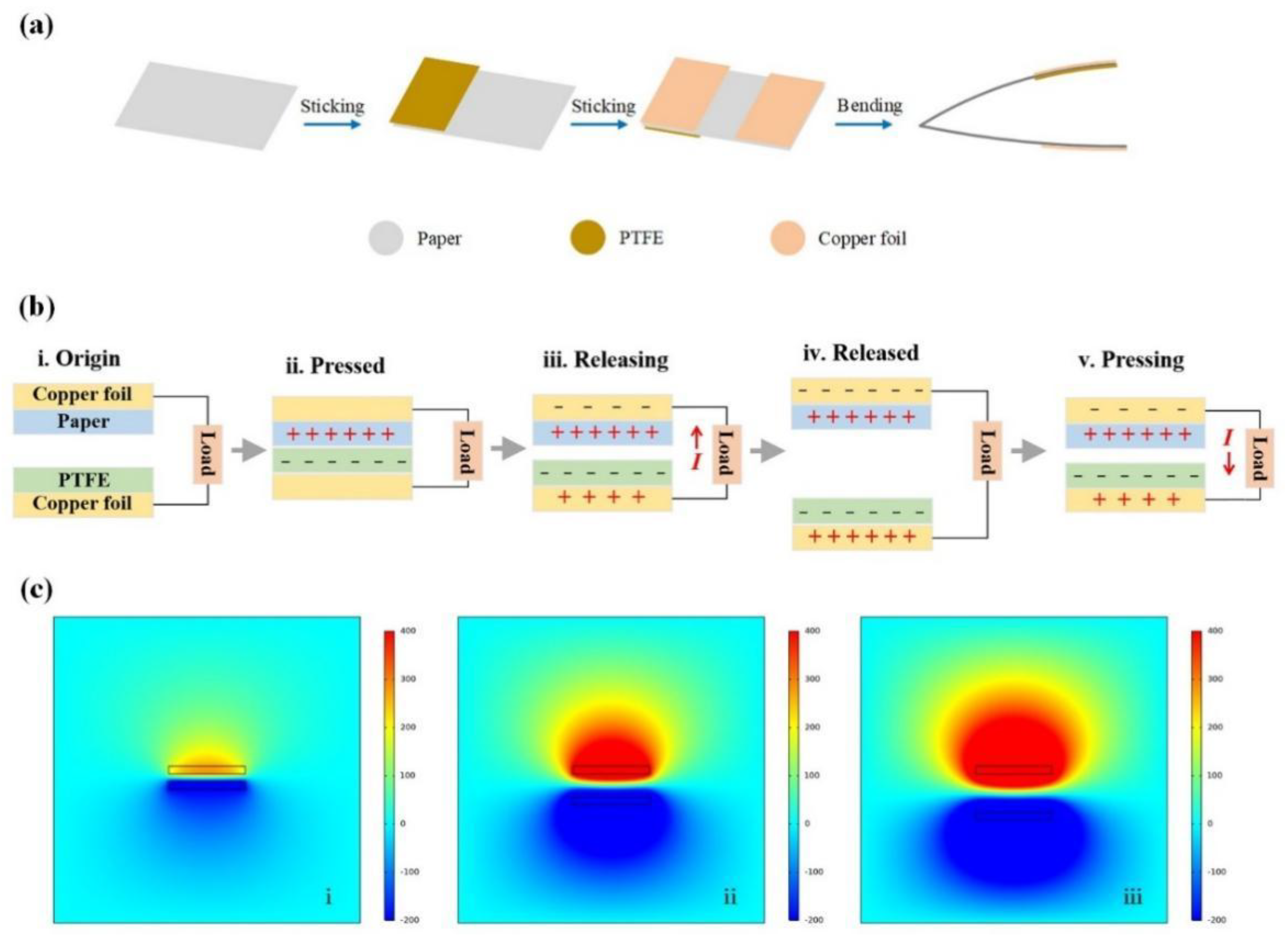
Figure 4.
(a) Output Voltage of TENG (b) Output Current of TENG (c) Load power of TENG (d) Load Current of TENG.
Figure 4.
(a) Output Voltage of TENG (b) Output Current of TENG (c) Load power of TENG (d) Load Current of TENG.
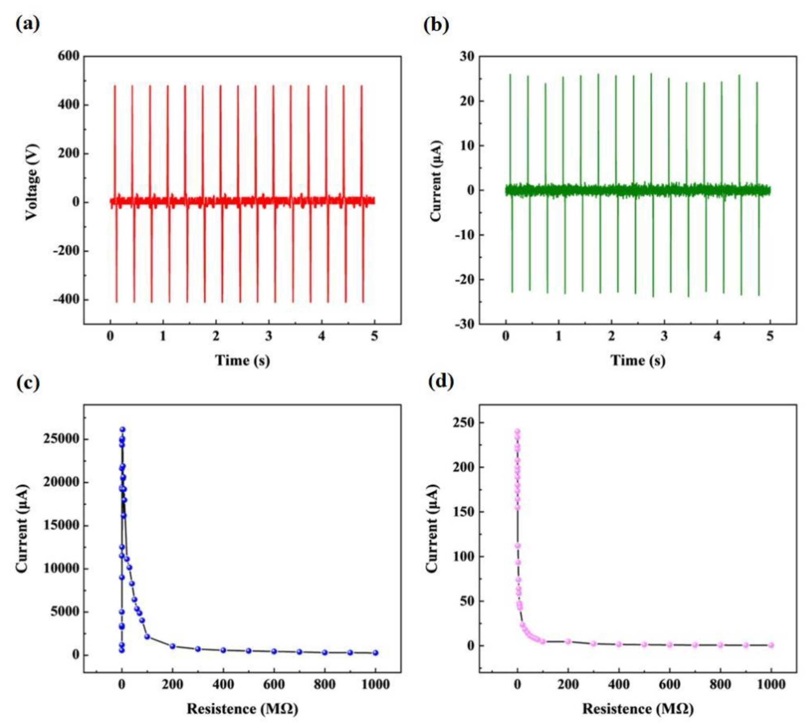
Figure 5.
Schematic diagram of human trigger signals recognition.
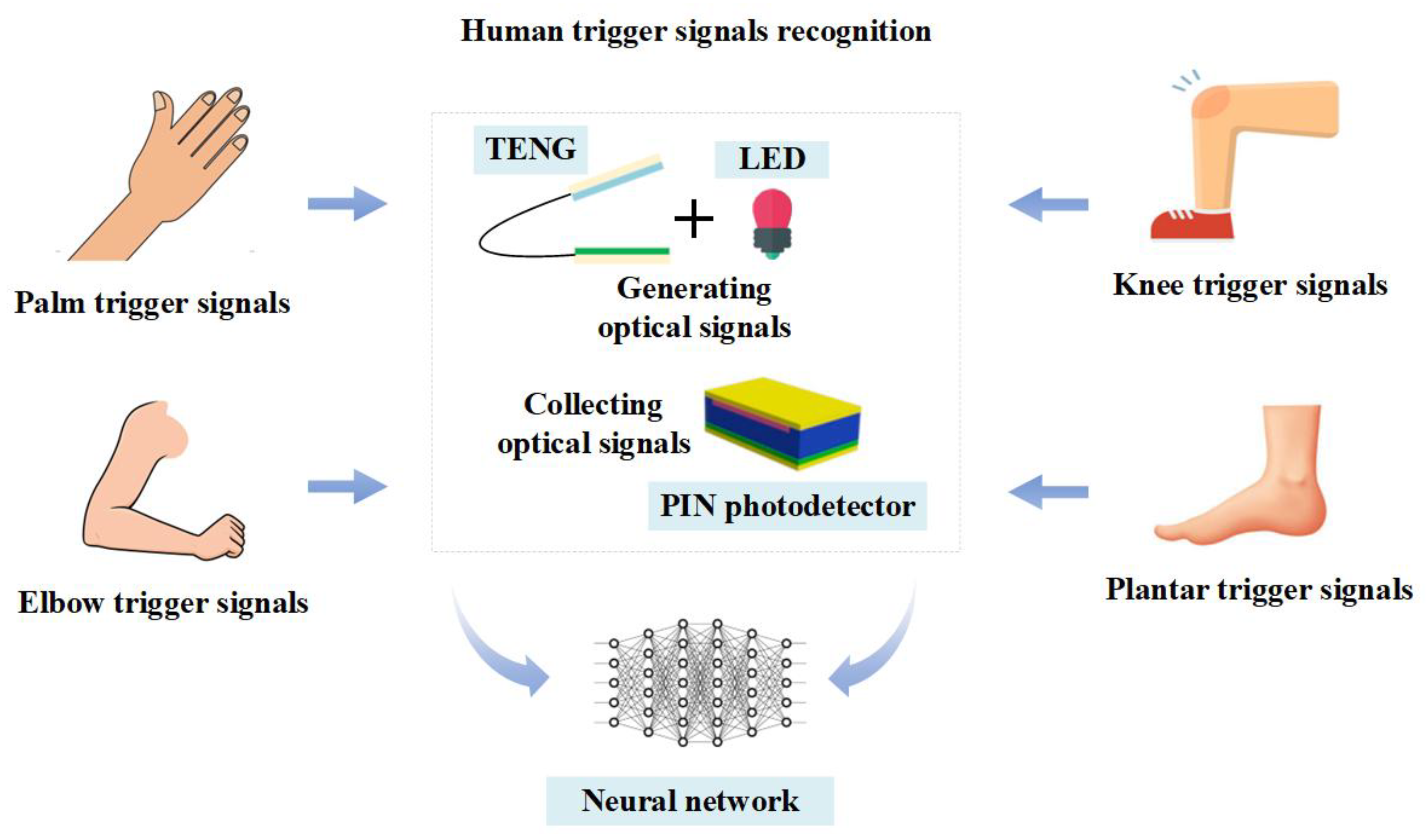
Figure 6.
Schematic diagram of the self-powered sensing system.
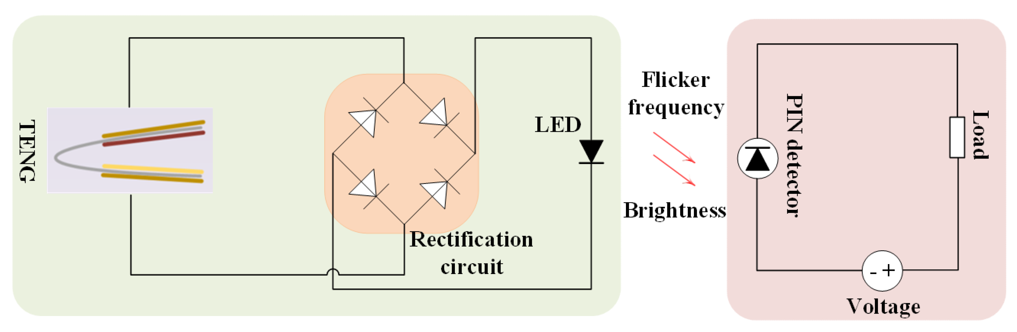
Figure 7.
CNN-LSTM fusion model network architecture.
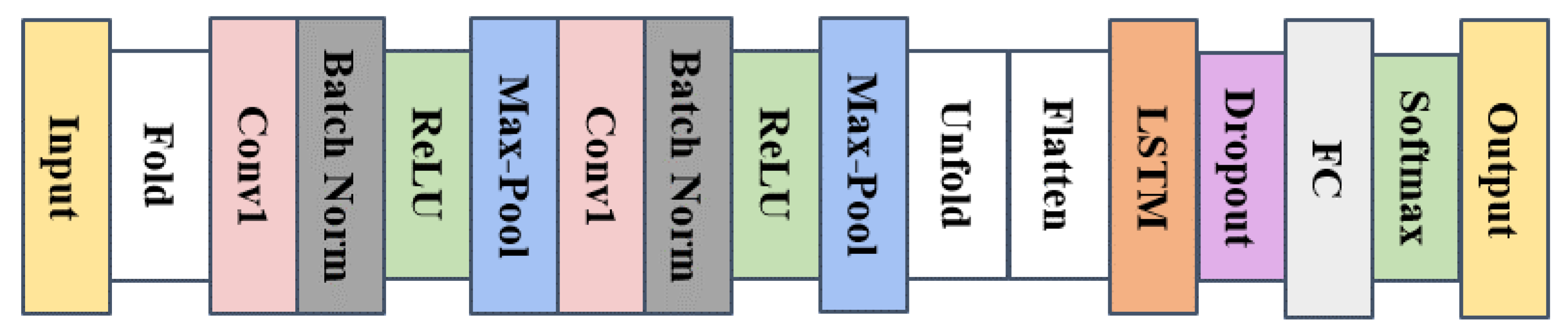
Figure 8.
Schematic diagram of data collection process.
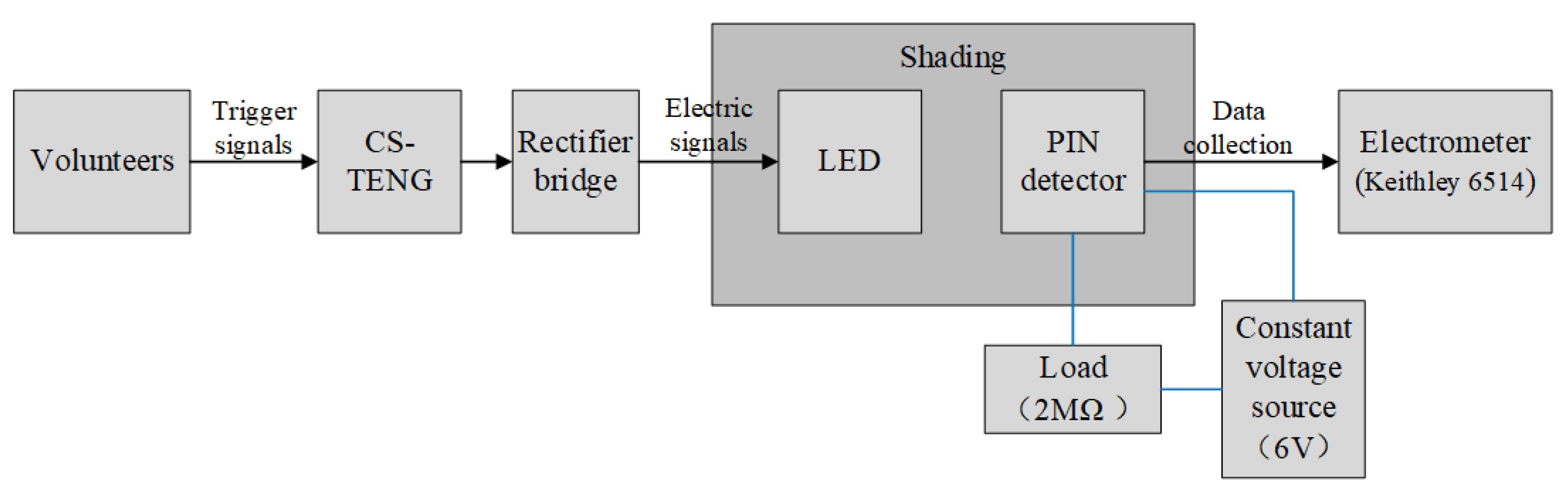
Figure 9.
CNN-LSTM model accuracy and loss function: (a) CNN-LSTM model accuracy; (b) CNN-LSTM model loss function.
Figure 9.
CNN-LSTM model accuracy and loss function: (a) CNN-LSTM model accuracy; (b) CNN-LSTM model loss function.
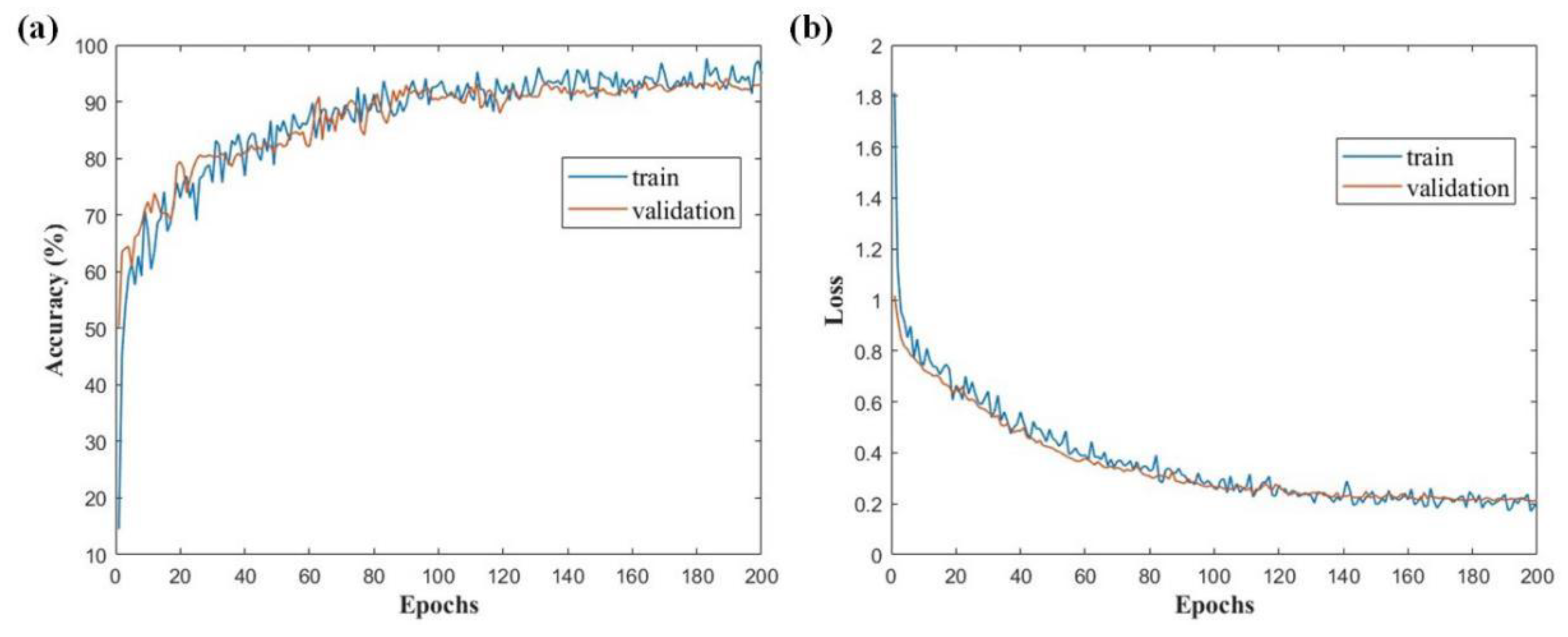

Table 1.
Hyperparameter settings of CNN-LSTM model.
| Layers | Types | Parameters |
|---|---|---|
| 1 | Input | - |
| 2 | Sequence Folding Layer | - |
| 3 | Convolution Layer 1 | 64 2×1 convolutions with stride [1 x 1] |
| 4 | Batch Normalization 1 | - |
| 5 | ReLU | - |
| 6 | Max-pool 1 | 2×1 pooling kernel with stride [2 x 1] |
| 7 | Convolution Layer 2 | 32 2×1 convolutions with stride [1 x 1] |
| 8 | Batch Normalization 2 | - |
| 9 | ReLU | - |
| 10 | Max-pool 2 | 2×1 pooling kernel with stride [2 x 1] |
| 11 | Sequence Unfolding Layer | - |
| 12 | Flatten Layer | - |
| 13 | LSTM Layer 1 | LSTM with 32 hidden units |
| 14 | Dropout | 25% dropout |
| 15 | Fully Connected | - |
| 16 | Softmax | - |
| 17 | Classification | - |
Table 2.
Model evaluation results.
| Models | Precision (%) | Recall (%) | F1-score (%) | Accuracy (%) |
|---|---|---|---|---|
| CNN | 88.01 | 88.69 | 88.12 | 87.94 |
| LSTM | 87.53 | 88.24 | 87.64 | 87.64 |
| CNN-LSTM | 92.92 | 93.35 | 93.11 | 92.94 |
Table 3.
Trigger signal category classification results.
| Models | Types | Precision (%) | Recall (%) | F1-score (%) |
|---|---|---|---|---|
| CNN | M | 97.96 | 96.39 | 97.17 |
| E | 69.71 | 84 | 76.19 | |
| W | 86.44 | 77.27 | 81.60 | |
| R | 97.91 | 97.10 | 97.50 | |
| LSTM | M | 97.37 | 94.47 | 95.90 |
| E | 68.94 | 83.94 | 75.70 | |
| W | 85.71 | 76.83 | 81.03 | |
| R | 98.10 | 97.73 | 97.91 | |
| CNN-LSTM | M | 95.18 | 95.56 | 95.37 |
| E | 86.46 | 90.83 | 88.59 | |
| W | 92.16 | 87.85 | 89.95 | |
| R | 97.88 | 99.14 | 98.51 |
Disclaimer/Publisher’s Note: The statements, opinions and data contained in all publications are solely those of the individual author(s) and contributor(s) and not of MDPI and/or the editor(s). MDPI and/or the editor(s) disclaim responsibility for any injury to people or property resulting from any ideas, methods, instructions or products referred to in the content. |
© 2025 by the authors. Licensee MDPI, Basel, Switzerland. This article is an open access article distributed under the terms and conditions of the Creative Commons Attribution (CC BY) license (http://creativecommons.org/licenses/by/4.0/).
Copyright: This open access article is published under a Creative Commons CC BY 4.0 license, which permit the free download, distribution, and reuse, provided that the author and preprint are cited in any reuse.


