
Submitted:
17 November 2025
Posted:
18 November 2025
You are already at the latest version
Abstract
Apart from combining two converters by connecting them in parallel at the input and the output sides, one can connect them in parallel at the inputs and in series at the outputs of the stages to increase the power rate and to modify the voltage transformation ratio. Four converter topologies with limited duty cycle range are studied for their application as stages for a converter combination which operates as an inverting two stage step-up converter. The operation of the converter combinations is studied in the steady state, the dynamic models (for large and small signals) are derived. The start-up of the converters is analyzed. The stress across the components is calculated, and hints for dimensioning are given. The considerations are proved by LTSpice simulations. The advantages and the disadvantages of the four converters are included.
Keywords:
two-stage converter
; limited duty cycle
; floating
; modelling
; large signal model
; small signal model
; voltage transformation ratio
1. Introduction
To increase the output power of a converter one can combine two converter stages. A common concept is to connect the converters in parallel as is displayed in Figure 1a. The voltage transformation ratio of the complete converter is equal to the one of the stages. The second concept is to connect the inputs of the stages in parallel and the outputs of the stages in series and including the input voltage. This is shown in Figure 1.b. The pointed line between one input terminal and one output terminal of the converter stages shows that they are directly connected. In this second concept the voltage transformation ratio is changed. The output voltage is now the sum of the two output voltages of the two stages and the input voltage
This concept leads to a large output voltage. It can be used when a stable input voltage is available. A sudden change at the input leads directly to a sudden change at the output. If one uses a diode in series to the input source and a capacitor behind the diode at the input of the two-stage converter, the direct influence can be avoided. The additional diode serves also as a reverse polarity protection.
Small letters in this paper symbolize the time variables. For the steady state one can write capital letters.
A third concept to combine two converters again is to connect the inputs in parallel and the outputs directly in series. This is depicted in Figure 2a. Now it is not possible to use the same converter type, instead one must use an inverting and a noninverting converter stage. The output voltage is given by
This concept can also be used by input voltages which are not stiff and can change fast. The control of the converter stages has to correct the output voltage. In the method according to Figure 1.b a change of the input voltage directly influences the output voltage.
A fourth concept is shown in Figure 2b. The inputs of the converters are connected in parallel. The converter stages have no direct connection between the input and the output sides (which is shown by the pointed line in the other concepts). So one has to combine the outputs in series. Here converters with isolation between input and output can be used.
Using two inverting DC/DC converters leads to a high voltage transformation ratio. In this paper inverting limited duty cycle step-up-down converters are used to produce a floating two-stage converter with high voltage transformation ratio. They are taken from [1], where 8 converters with reduced duty cycle range which are grounded to the positive input terminal are presented. Two of them are step-down, two of them are step-up and four of them are inverting step-up-down converters. These converters can be combined with stages, where the ground is connected to the negative input terminal.
The aim of this paper is to show four new floating two-stage converter topologies according to Figure 1b with a high voltage transformation ratio. Two different voltage transformation ratios are achieved. The new floating converters are studied in detail.
In the Chinese patent application [2] a converter according to Figure 1.b consisting of two Boost converters is presented and the modes are described in detail. A more complicated converter with the same connection at the inputs and the outputs of the stages can be found in [3]. Each stage consists of n bidirectional Boost converters which are connected in parallel. So a large output power can be produced. Another Chinese patent application [4] shows a floating converter consisting of Boost converters with an additional capacitor, a diode and a winding, which is magnetically coupled with the winding used in the Boost converter. [5] shows a modification of the Boost converter which is used for the stages of a converter according type Figure 1.b. The advantage of this circuit is that compared to the normal Boost converter no inrush current occurs when connected to the input voltage. A publication concerning the concept according Figure 2.b is [6]. A complex converter is shown, where the active switches are working against ground and the capacitors are connected in series. Instead of the coils used in a Boost converter, here they are replaced by transformers. The secondary sides of the transformers are used to make an additional step-up of the output voltage. [7] shows a two-stage converter, where the stages are constructed by tristate Boost converters. The tristate concept applied to a step-up converter makes it possible that it becomes a phase-minimum system, when the converter is controlled in a special way (c.f. [8].) A converter consisting of two step-up stages, each built of one active switch, two diodes, two capacitors and two coupled coils is treated in [9]. [10] shows several bidirectional floating and interleaved converters which are built from bidirectional Boost converters. A quadratic Boost with two stages is treated in [11]. The circuit is very complex. The design and the analyzes of a floating converter (type 1.b) is done in [12]. The stages need one active switch, four diodes, two coils, and three capacitors. The extension of a floating two-stage Boost converter by resonance circuits is explained in [13]. The main inductor of the Boost converter is here split into two magnetically coupled windings which form a resonance circuit with an additional capacitor.
2. Floating Two-Stage Converter Type I
2.1. Basics
Two converter stages are connected in parallel at the inputs and in series with the input at the output side. The circuit diagram is shown in Figure 3.
Inspecting the loop consisting of C1, L2, C2 and L1 (this is the same whether one looks at stage one or stage two), and keeping in mind that in the stationary case the voltage across an inductor is zero in the mean, results in the fact that the voltages across the capacitors must be equal
The voltage-time balance across the first inductor can be found according to
The index i stands for the number (1 or 2) of the stages of the converter leading to the output voltage of the stage in compliance with
The duty cycle must be lower than a half. In practice, one will limit the duty cycle to 0.4. The output voltage of the complete converter is the sum of the output voltages of the two stages and the input voltage. For the complete converter the output voltage results in
Figure 4 shows the voltage transformation ratios of the complete converter, which is larger and of one stage which is the lower one.
2.2. Model with Included Losses
The two stages are controlled by signals which are shifted by 180 degrees. For the model we need only one stage. Here the lower stage is used. An equivalent resistor R is used as load. Figure 5 shows the equivalent circuit of the second stage.
For the calculation we skip the 2 of the second stage. First the current through the output capacitor is calculated with the help of KCL according to
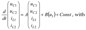
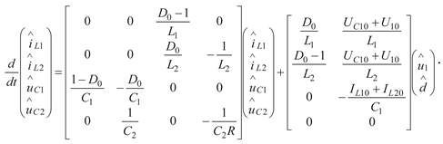
Now the four state equations are given according to
Combining into a matrix differential equation leads to
The equivalent circuit of mode M2 is depicted in Figure 6.
One gets for the four state equations
Combining into one matrix differential equation gives
The two systems can be combined by weighting the equation (12) for mode M1 by the duty cycle and (17) by one minus the duty cycle. This results in
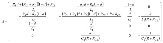
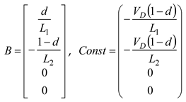
with the state matrix A, the input matrix B and the constant vector Const
2.3. Simulation in the Steady State
Figure 7 shows the input current, the current through the second coil of the second stage, the current through the first coil of the second stage, the current through the second coil of the first stage, the current through the first coil of the first stage, the input voltage, the control signal of the second stage, the control signal of the first stage, and the output voltage. The control signals are shifted by 180 degrees. The frequency of the input current therefore has double the frequency of the stages.
The simulation of one stage can be also executed by an equivalent resistor for the second stage.
Figure 8.
Steady state simulation with an equivalent resistor: (a) simulation circuit, (b) top to bottom: input current (dark violet), load current (brown); current through second coil of the second stage (black), current through the first coil of the second stage (grey); input voltage (blue), control signal of the second stage (dark green), output voltage (green).
2.4. Dynamic Simulation
Figure 9 shows the simulation circuit used for the dynamic simulations. The pwm signals are produced by the comparators U1 and U2. Triangle signals are used as carrier signals which are shifted by 180 degrees. The floating drivers of the active switches are modelled by the voltage-controlled voltage sources E1 and E2. They have a gain of ten to amplify the pwm signals.
Figure 10 shows the start-up by increasing the duty cycle starting from zero, duty cycle steps, and input voltage steps. One can see the current through the second coil of stage one, the current through the first coil of stage one, the duty cycle (both stages are controlled by the same duty cycle), the input voltage, and the output voltage.
The duty cycle steps lead to a high overcurrent through the coils. Therefore, the duty cycle must be changed by a ramp. This is shown in Figure 11. It should be mentioned that the parasitic resistor of the coils is RL=4 mΩ, and of the capacitors it is RC=10 mΩ. Again the start-up, the duty cycle changes and the steps of the input voltage are shown. The signals are the current through the second coil of stage one, the current through the first coil of stage one, the duty cycle, the input voltage, and the output voltage.
2.5. Simulation by Solving the Differential Equation (18, 19)
This simulation is much faster than the simulation by the circuit and displays only the mean value of the signals and not the ripple. Figure 12 shows the circuit used. The integration is done by a current through a capacitor of 1 F. The parallel resistor of 10 MΩ serves only for stabilizing. The derivative is written as current of an arbitrary current source B. With the voltage controlled current sources L1 and L2, the voltage of the integrator is transferred into a current, so currents are seen in the result.
Figure 13 shows the result. The signals shown are: the current through second coil of the first stage, the current through first coil of the first stage, the duty cycle, the input voltage, and the output voltage. Both simulation methods lead to the same results.
2.6. Idealized Model
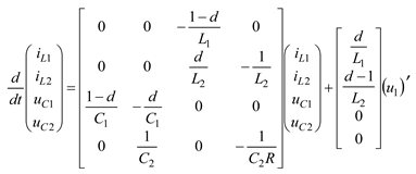
Setting all parasitic resistors and the forward voltage of the diode in (18) to zero describes the idealized model. One obtains
The linearized model around the operating point is given by
The connections between the operating point values are for the voltages
This leads to
For the currents one gets
Keep in mind that the results describe one stage alone.
2.7. Inrush
When the converter is connected to a stable input voltage, no inrush current occurs, an advantage compared to the other three types treated here. This is shown in Figure 14, where the input current, the input voltage, the output voltage of the two stages and the output voltage of the complete converter are shown.
The voltage across the load is about the same as the input voltage. A steady state current is flowing through the load. The current flows through the loop consisting of U1, L22, D2, load R, D1 L21. A small ringing occurs, but the converter has no problem, when applied to a stable input voltage.
2.8. Dimensioning Hints for the Converter Type I
For the dimensioning the voltage stress of the semiconductors is important. With KVL one gets for the active switch when the diode is conducting
The same stress occurs across the diode when the transistor is on. For the coils one can choose a current ripple ΔI and the switching frequency f. The signal of the voltage across both coils of one stage is the same. So one can dimension the coils according to
The output capacitors have only to smooth the current ripple of the output coil and have the value
This is the equation for the ideal capacitor. For the correct choice of the value one must look at the series resistor of the capacitor. Typically, the value to achieve a desired maximum voltage ripple is about three times of this value.
During the on-time of the switch the first capacitor is discharged by the current through the second coil. The mean current through the first coil is equal to the load current. For the charge balance through C1i one obtains
The mean value of the current through the second coil is therefore
For the first capacitor one gets
2.9. Interleaved Converter Type I
A second way to combine two converters is by connecting them in parallel. The control signals are shifted by a half period. The so realized converter again has no inrush current, when connected to a stable input source. The capacitors can be slowly charged by increasing the duty cycle from zero to the desired value. The voltage transformation ratio of the complete converter is only that of one stage
The graph is shown in the lower line of Figure 3. The converter is an inverting step-up-down converter. The output voltage is significantly lower than that of the floating converter. The reference, however, is the same for both stages. One can also use more than one stage in parallel, when larger output power is desired. Figure 15 shows the dynamic behavior during start-up, changes of the duty cycle, and steps of the input voltage. The signals shown are: the currents through the coils, the duty cycle, the input and the output voltages.
Figure 16a shows the converter in the steady state. Depicted are: the input current which has double the frequency of the frequency of the stages, the current through the coils of both stages, the input voltage, the control signals of the switches, and the output voltage. Figure 16b shows the start-up, changes of the duty cycle and steps of the input voltage. The simulation is done by solving the differential equation. One can see that it is wise to change the duty cycle by ramps and not by steps.
3. Floating Two-Stage Converter Type II
3.1. Basics Type II
There exists a second circuit to obtain the same voltage transformation ratio of
The diagram of the voltage transformation ratio is therefore again equal to Figure 3.
The circuit diagram is shown in Figure 17.
In the steady state the voltage across the first capacitor is equal to the sum of the input voltage and the output voltage of the stages
With the help of the charge balance at the first capacitor one gets a connection between the currents through the coils according to
The charge balance of the second capacitor is given by
The mean values of the current through the coils referred to the load current can now be calculated according to
3.2. Model of Type II
The model can be calculated in the same way as is shown in the previous section and leads to state matrix A, the input matrix B, and the constant vector Const according to
3.3. Simulation in the Steady State Type II
Figure 18 shows the currents through the stages one and two, the load current, the input voltage, the control signals, and the output voltage.
3.4. Dynamic Simulation Type II
The used simulation circuit is depicted in Figure 19.a. It is similar to the one used in section II.
The results are shown in Figure 19.b. The currents through the coils of the first stage are shown, in addition the duty cycle, the input voltage, the output voltage of stage one, and the output voltage of the complete two-stage converter. The results from stage two are not shown because they are equal.
The dynamics of the two stages are similar.
3.5. Idealized Model Type II
By setting the parasitic resistors to zero, one gets an idealized model
Linearization around the operating point leads to the small signal model and the connections between the operating point values (for one stage)
3.6. Inrush Type II
A disadvantage of this converter type is the inrush current. This version has a significant inrush overcurrent and ringing compared to the converter described in section II. Connecting the converter immediately to a strong stable input source is shown in Figure 20.a. The input current, the currents through the coils, the output voltages of the complete converter and the stages now show a pronounced ringing and a significant overcurrent.
A way to avoid the inrush is to connect a Buck converter in front of the two-stage converter. The voltage can now be increased by a ramp. This shown in Figure 20.b. The same signals as in Figure are depicted. The Buck converter only has to work during the start-up. Afterwards the switch of the Buck converter is always conducting. In case of an error this switch can be used as an electronic fuse. The Buck converter is simplified in the simulation by a ramp of the input voltage.
4. Floating Two-Stage Converter Type III
4.1. Basics Type III
Combining two (2d-1)/(1-d) converters as shown in Figure 21 leads to the voltage transformation ratio
The restriction of the duty cycle is caused by the restriction of the stages. It cannot be seen directly in the equation.
In the steady state the voltage across the first capacitor of a stage is the sum of the input and the output voltages
The mean value of the current through the second coil is equal to the output current. The output capacitors of the stages have only to smooth the ripple of the current through the output coil. The charge balance of the first inductor is again the same as for type I and is shown in (29). So the dimensioning hints given in section II also assist in the designing of type III.
Figure 22 shows a diagram of the voltage transformation ratio of the complete converter (the larger one) and of one stage.
4.2. Model with Equivalent Resistor Type III
Both stages are driven by the same duty cycle. The control signals of the two stages are shifted by 180 degrees. The load R is an equivalent resistor representing the load of one stage of the converter. During mode M1, when the active switch is turned on, the equivalent circuit of the second stage is given in Figure 22.
For the calculation we skip the 2 of the second stage. The current through the output capacitor can be found with KCL according to
The state equations are
Combination leads to the matrix differential equation
The equivalent circuit of one stage (the second stage is used) during mode M2 (the active switch is off and the diode is conducting) can be seen in Figure 23.
The current through the output capacitor is the same as in mode M1. The state equations can be found with Kirchhoff’s laws according to
The equation for the change of the voltage across the output capacitor is equal to the one given of mode M1 (47).
Summarization into a matrix equation gives
In the continuous mode, it is easy to combine the two matrix equations (51) and (55) by weighting the first one by the duty cycle d and the second one by 1-d. Solving the result of this operation (called state space averaging) leads to a model which can be calculated much faster than the circuit simulation. Only the mean values are shown. With the state vector x, the input vector u (which is in our case only the input voltage), the state matrix A, the input matrix B, and a constant vector which includes the constant part of the forward voltage of the diode one gets
4.3. Idealized Model with Equivalent Resistor Type III
In a first step one can use the idealized model, which is obtained by setting all parasitic resistors to zero, for calculating the transfer functions. The idealized large signal model can therefore be written according to
Linearization around the operating point (marked by capital letters) leads to the small signal model (the disturbances are marked by hatted small letters)
The small signal model now has two input variables, the input voltage and the duty cycle. For the connections between the operating point values of one stage one get
The output current is equal to the currents through the output coils of the stages.
4.4. Simulation Type III
4.4.1. Steady State
The steady state is shown in Figure 24. Depicted are: the input current, the currents through the coils of stage 2, the load current; in the next graph: the currents through the coils of stage 1 and the load current; and in the final graph: the absolute value of the output voltage, the voltage across the output capacitor of stage 1, the input voltage, and the control signals of the switches.
4.4.2. Dynamic Analyzes
Figure 25 shows the start-up, changes of the duty cycle and steps of the input voltage. Depicted are: the current through the second coil, the current through the first coil, the duty cycle, the input voltage, the output voltage of stage 1, and the output voltage of the complete converter. The ramp of the duty cycle should be slower to avoid the overcurrent through the first coils of the stage during start-up.
In Figure 26 there are the same signals shown, but calculated with the differential equation (53). The voltages show a good coincidence. The ringing of the currents is more pronounced and reaches negative values, caused by the fact that in the circuit the diodes stop the current, but that in the model the current can ring freely. When the duty cycle changes with a ramp, both simulation results are equal.
4.5. Inrush Type III
As can be seen in the figures 25 and 26, an inrush occurs. One can see the pronounced ringing through the coils and the transients of the voltages at the output of the stages and at the output of the complete converter.
During inrush the output capacitors are charged to half of the input voltage; the output voltage is therefore zero. The output voltages of the two stages are not inverted.
To avoid problems with the inrush, the input voltage can be increased linearly by a pre-stage. This is demonstrated in Figure 27. The ramp takes 50 ms and so the input current is only small. The voltages change without ringing in the used scale.
5. Floating Two-Stage Converter Type IV
5.1. Basics Type IV
The second topology to achieve the voltage transformation ratio according to
is shown in Figure 28.
The graph of the voltage transformation ratio can be found in Figure 22.
5.2. Steady State Type IV
Figure 29 shows the behavior of the converter in the steady state. It works similar to type 5. The input current is pulsating, but always flowing into the converter. One can see the large output voltage compared to the input voltage. Shown are the input current, the currents through all coils, the output current, the input voltage, the control signals, and the output voltage.
5.3. Dynamic Simulation Type IV
The dynamic simulation (Figure 30) shows the typical behavior of the here treated converters.
5.4. Model with Equivalent Resistor Type IV
The state matrix A, the input matrix B and the constant vector are given as follows:
The idealized model can easily be found by setting the parasitics to zero. From this idealized model the transfer functions can be obtained. Figure 31 shows the currents through the coils, the duty cycle, the output voltage of one stage, the input voltage, and the output voltage of the complete converter.
Setting the input voltage and the duty cycle constant, one can easily draw the Bode plot for that operating point. This is shown in Figure 32. A fourth order converter has two conjugate complex poles which shift the phase by minus 360 degrees. The poles can be seen as the two resonances. The transfer function has three zeroes. One of them is conjugate complex and is on the left side of the complex plane. It shifts the phase by plus 180 degrees, and the third zero is on the right side of the complex plane and causes a phase shift of minus 90 degrees. At high frequencies the phase of the converter tends towards minus 270 degrees. Bode diagrams are important for the design of controllers.
5.5. Inrush Type IV
5.6. Influence of the Tolerances
The influence of the tolerances is shown for type IV, but is also valid for the other three types. Figure 35 shows the input current, the currents through the coils, the load current, the input voltage, the control signals and the output voltage, when the values of the inductors of the second stage differ from those of the first stage by plus/minus 10 %. The slopes of the current are changing, but the load current and the output voltage stay constant compared to Figure 29.
Figure 36 shows the same signals as before, but now the output voltages of the stages are included and the duty cycle of the stages differs by 5 %. The stage with the larger duty cycle has the higher output voltage. The output currents are still equal. This automatic symmetrizing is a great advantage of these converter types. In case of the interleaved converter with parallel connections of the stages, a large asymmetry of the output currents of the stages occurs.
6. Conclusions
The methods used to study the circuits:
- Basics found by inspecting the circuits in the steady state
- Circuit simulation with the help of LTSpice for the steady state and for the transients; the calculation time is long
- Calculating a state space averaging model and solving the differential equations again by LTSpice; the calculation time is short and the results are correct, when the changes are so small that the converter stays in the continuous mode
- Bode plots can be fast and easily achieved from the circuit which solves the differential equations
- An error in the state space model can be immediately found by the results of the simulation used
Interesting features of the treated converters:
- They are floating, that means one can take a terminal of the input side or of the output side as reference.
- Higher voltage transformation ratio, because the two output voltages of the stages plus the input voltage are added
- Two different voltage transformation ratios can be achieved
- The duty cycle of the stages is limited, it must be lower than 0.5 for the types I and II, and higher than 0.5 for the types III and IV
- The voltage stress of the components of the stages is lower than the voltage across the output of the complete converter; the stages have to be dimensioned only for half of this voltage
- The output current of the stages is equal to the load current, and symmetrizes the current through the stages
- The output voltage is directly influenced by the input voltage. To reduce this, a reverse polarity protection consisting of a diode and a capacitor has to be connected between the source and the converter
- Type I has the additional advantage that the start-up is easy when slowly increasing the duty cycle from zero to the desired value; no inrush current occurs. All other types need a pre-stage, when the start-up is problematic. Therefore, type I was studied more comprehensively
Funding
This research received no external funding.
Data Availability Statement
data are included in the paper.
Conflicts of Interest
The author declares no conflicts of interest.
References
- Himmelstoss, F. A. Converters with Reduced Duty Cycle Range and Ground Connected to the Positive Input Voltage Terminal. WSEAS Transactions on Circuits and Systems, vol. 23, pp. 239-251, 2024. [CrossRef]
- CN 119210154 A (NANTONG WOTEI NEW ENERGY CO LTD, 27.12.2024).
- CN 208241575 U (WETOWN ELECTRIC GROUP CO LTD; 14.12.2018).
- CN 107517003 A Output-floating input-parallel high-gain Boost converting circuit and switching method thereof (UNIV JIANGSU 26.12.2017).
- Himmelstoss, F. Modifizierter schwebender doppelter Hochsetzsteller AT 527723 B1, 15.6.2025.
- Ajmal, M. et al. A Parallel Input Series Output DC/DC Converter with High Voltage Gain. International Research Journal of Engineering and Technology (IRJET), 30.4.2017, Bd. 4, Nr. 4, pp 54-59.
- Zhang, C.; Xu, M.; Wang, W.; Meng, X.; Kan, Z. A High-gain Floating-Interleaved Three-level Boost Converter. 2019 4th International Conference on Intelligent Green Building and Smart Grid (IGBSG), Hubei, China, 2019, pp. 126-131. [CrossRef]
- Himmelstoss, F.A. Reduced Loss Tristate Converters. Electronics 2025, 14, 1305. [CrossRef]
- Guesmi, S.; Hanini, W.; Ghariani, M. Improved of Electrical Performance of Floating Output Interleaved Converter applied in Photovoltaic Application. 2022 International Conference of Advanced Technology in Electronic and Electrical Engineering (ICATEEE), M'sila, Algeria, 2022, pp. 1-6. [CrossRef]
- Lima, L. R. d.; Alcântara, P. A. de; Soares, L. C. S.; Barros, C. M. V.; Barros, L. S. Performance Analysis of Interleaved Bidirectional DC-DC Converters for Battery Control in Islanded Microgrid. 2023 IEEE Power & Energy Society General Meeting (PESGM), Orlando, FL, USA, 2023, pp. 1-5. [CrossRef]
- Li, Q. et al. An Improved Floating Interleaved Boost Converter with the Zero-Ripple Input Current for Fuel Cell Applications- IEEE Transactions on Energy Conversion, vol. 34, no. 4, pp. 2168-2179, Dec. 2019. [CrossRef]
- Allehyani, A. Design and Analysis of a High-Gain, Transformerless DC-DC Converter. 2024 IEEE Energy Conversion Congress and Exposition (ECCE), Phoenix, AZ, USA, 2024, pp. 197-203. [CrossRef]
- Sumukh, S. S A; Rao, B. T.; De, D.; Castellazzi, A. GaN Switch Based Novel Quadratic-Double-Boost Floating-Input High Gain DC-DC Converter 2024 Energy Conversion Congress & Expo Europe (ECCE Europe), Darmstadt, Germany, 2024, pp. 1-8. [CrossRef]
Figure 1.
Possibilities to combine two DC/DC converters connected in parallel at the input sides: a. interleaved; b. floating with serial outputs and input voltage included.
Figure 1.
Possibilities to combine two DC/DC converters connected in parallel at the input sides: a. interleaved; b. floating with serial outputs and input voltage included.
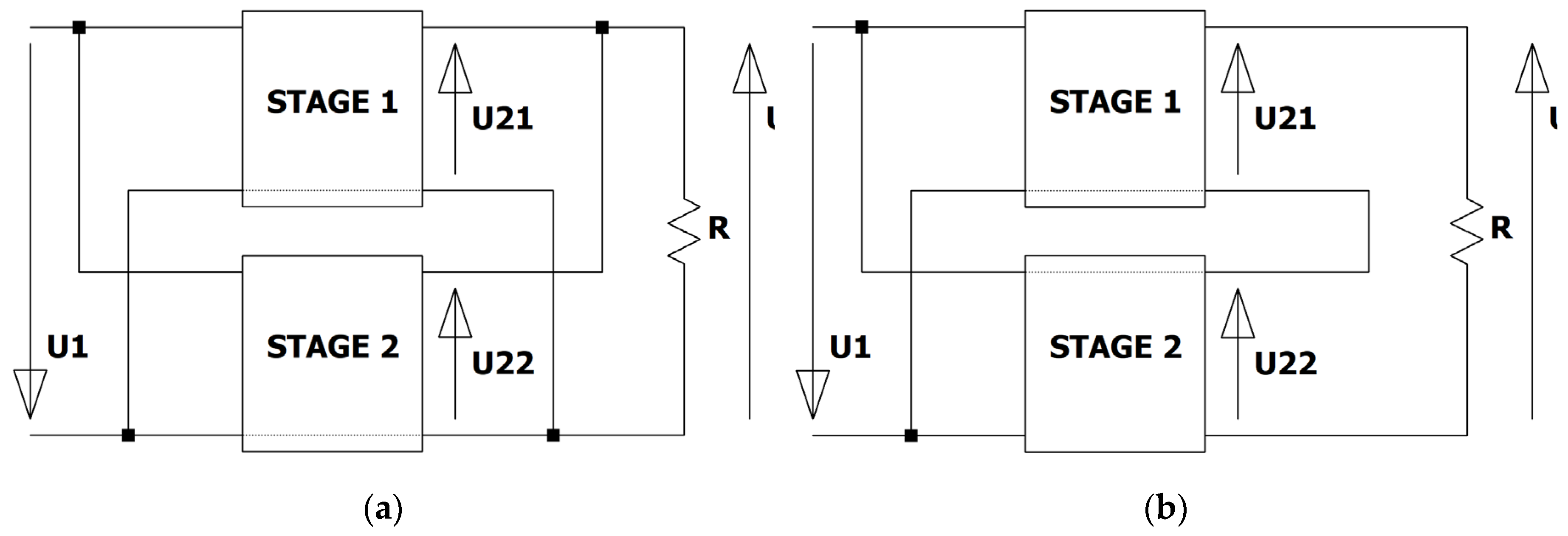
Figure 2.
Possibilities to combine two DC/DC converters connected in parallel at the input sides: a. floating with series output; b. combination with serial output.
Figure 2.
Possibilities to combine two DC/DC converters connected in parallel at the input sides: a. floating with series output; b. combination with serial output.
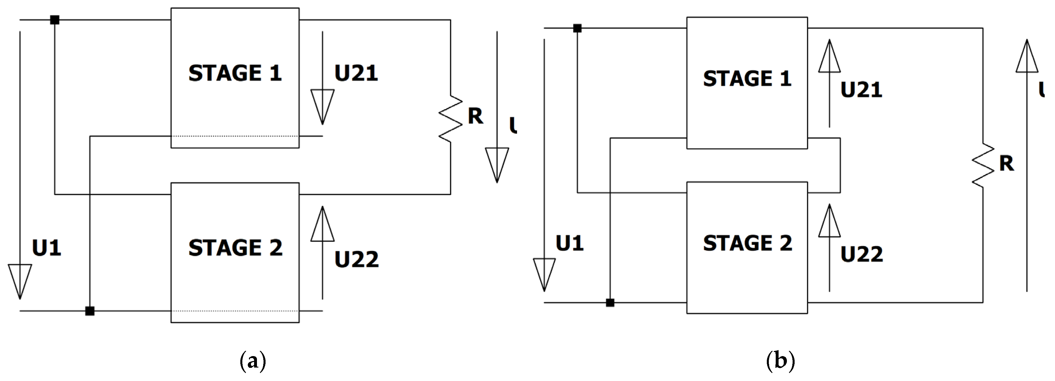
Figure 3.
Circuit diagram of the floating two-stage inverting Boost converter type I.
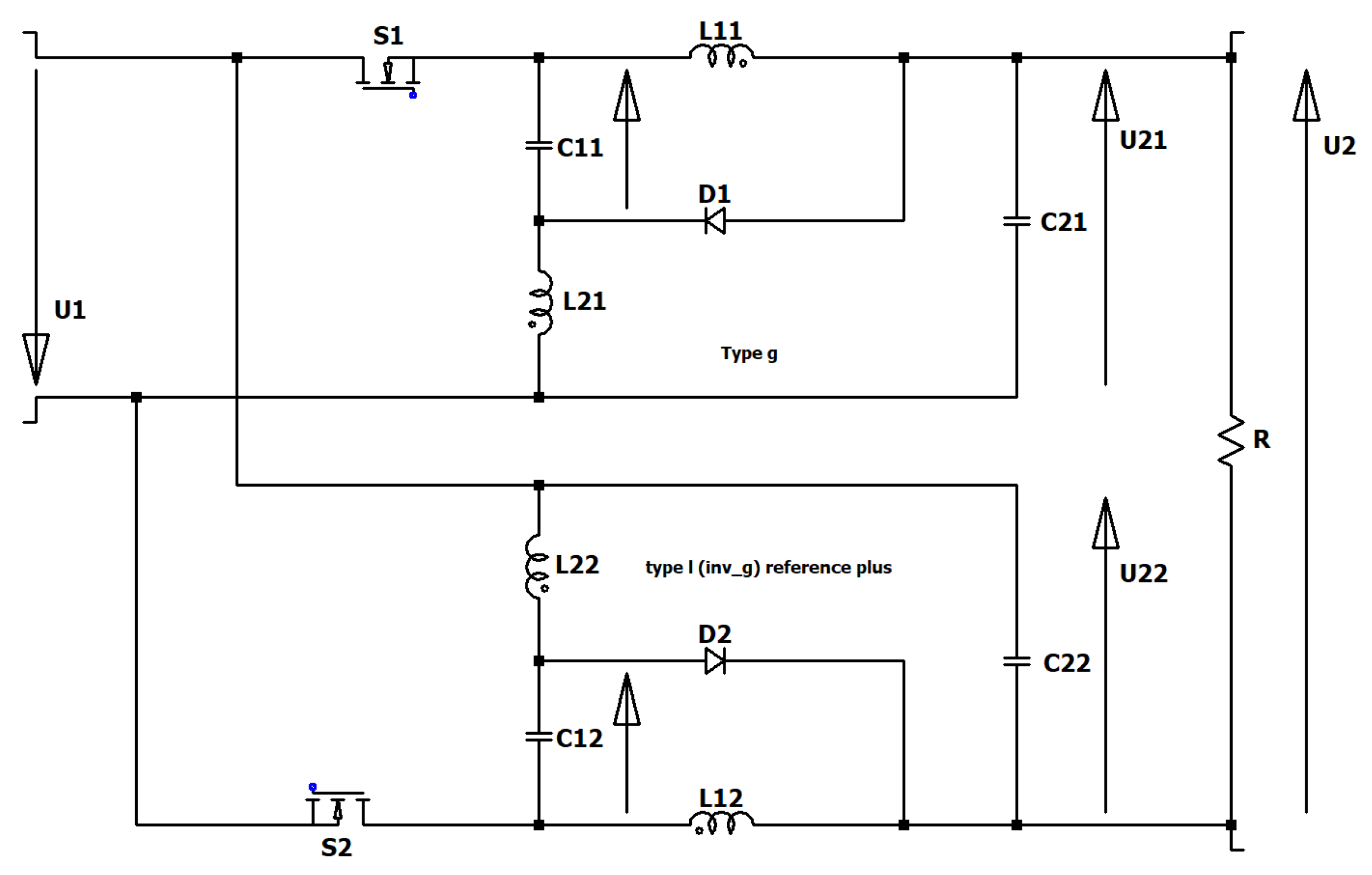
Figure 4.
Voltage transformation ratio M in dependence on the duty cycle; lower line: M of one stage and the higher line: M of the complete converter.
Figure 4.
Voltage transformation ratio M in dependence on the duty cycle; lower line: M of one stage and the higher line: M of the complete converter.
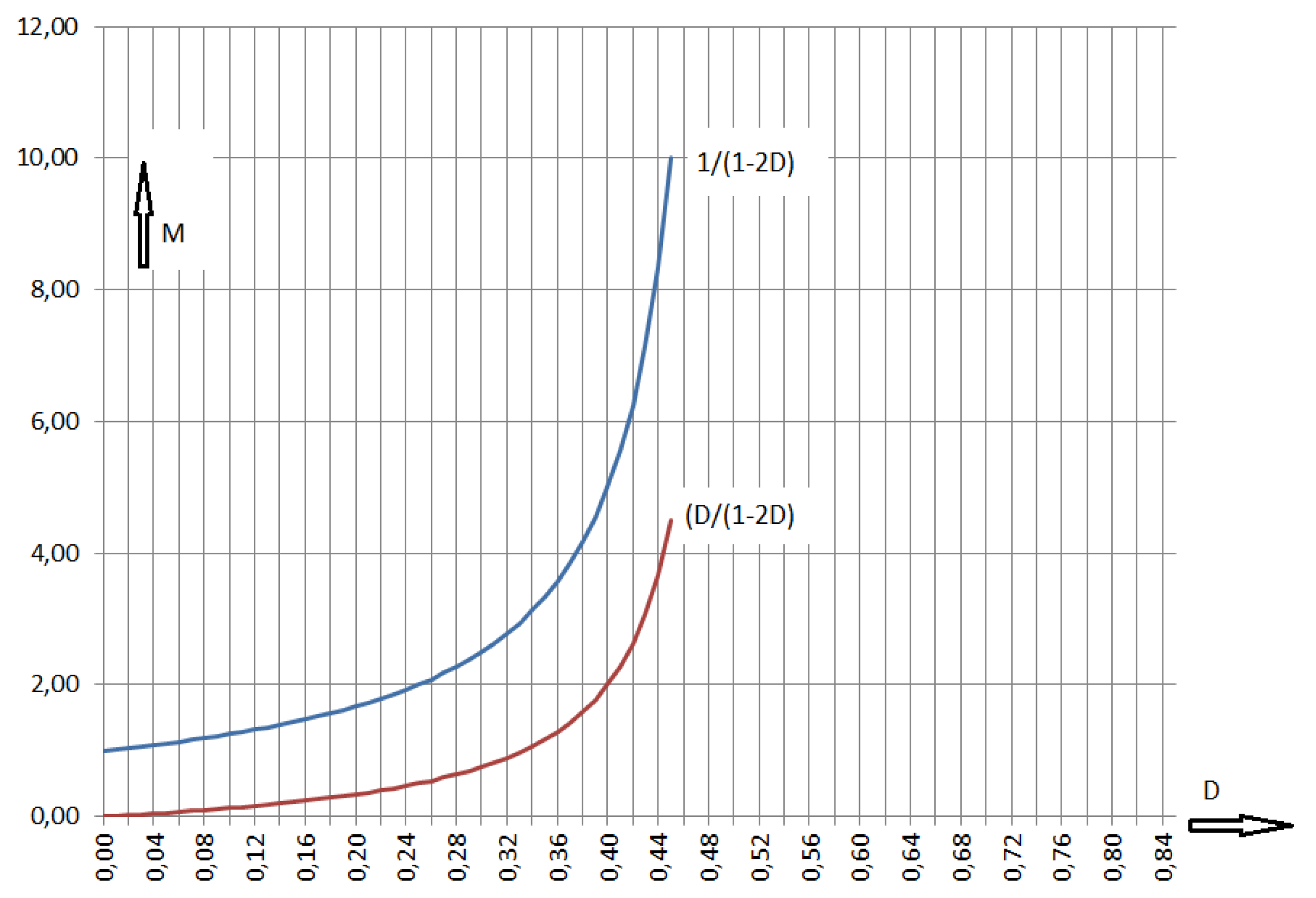
Figure 5.
Type I: Model with equivalent resistor, mode M1.
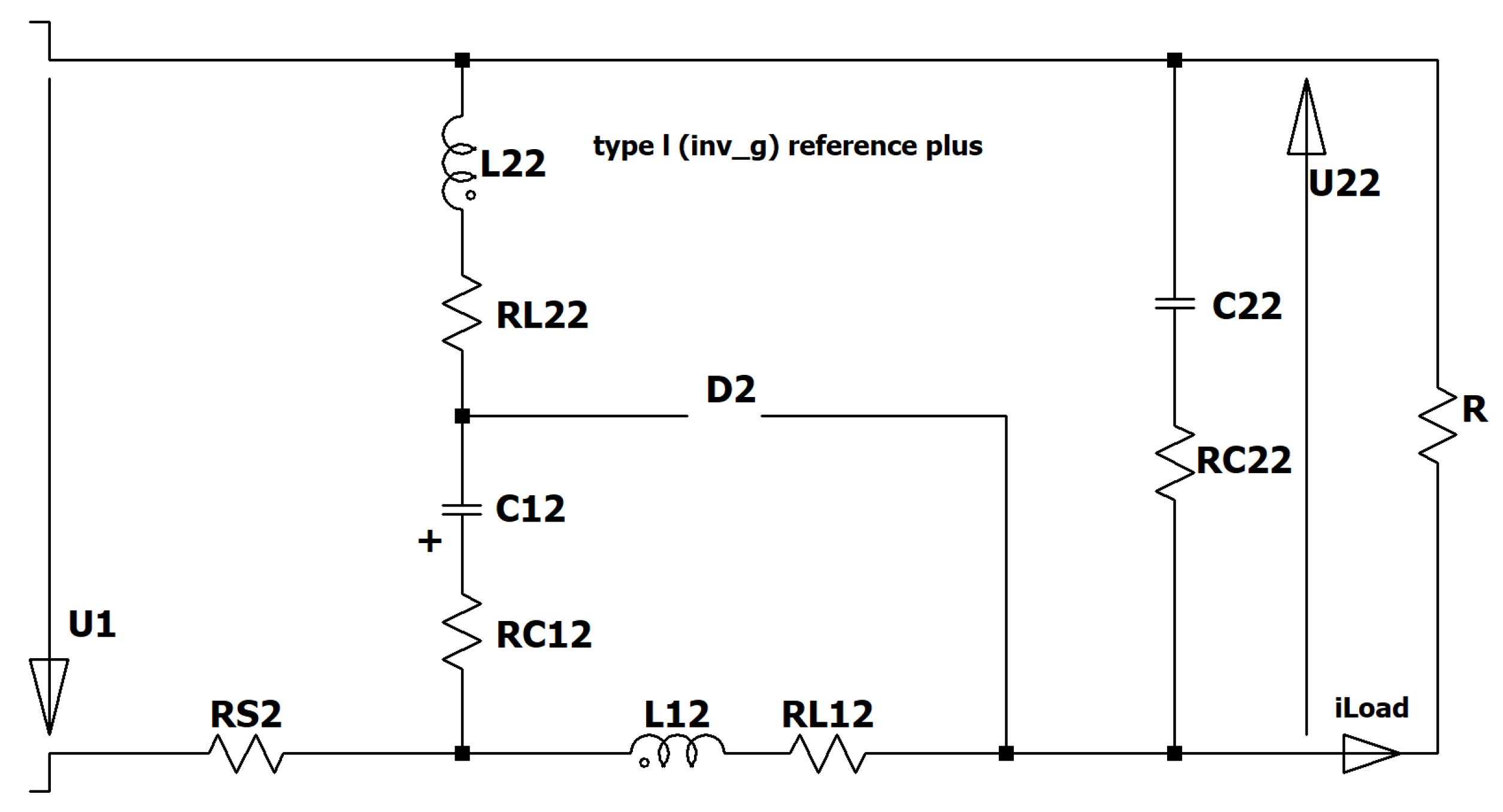
Figure 6.
Type I: model with equivalent resistor, mode M2.
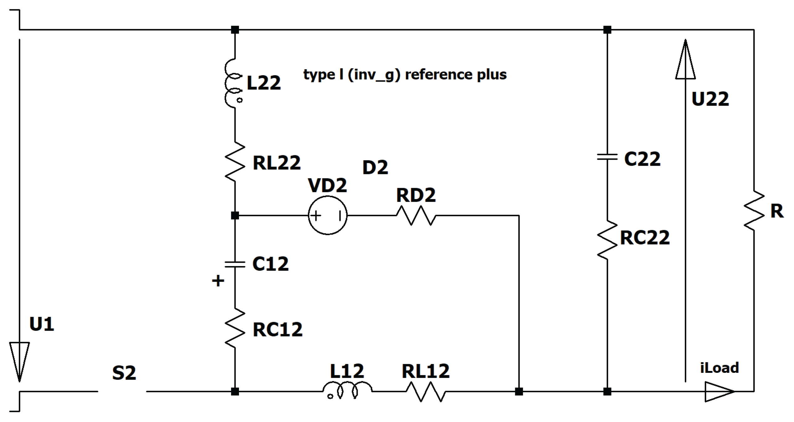
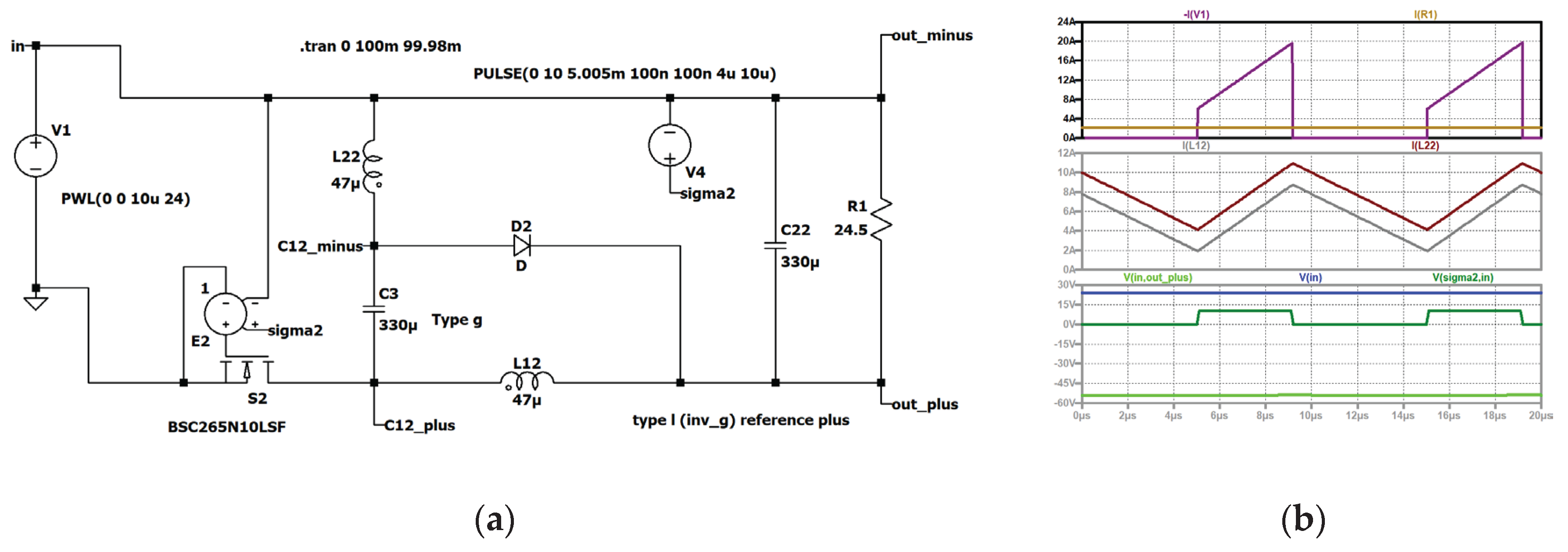
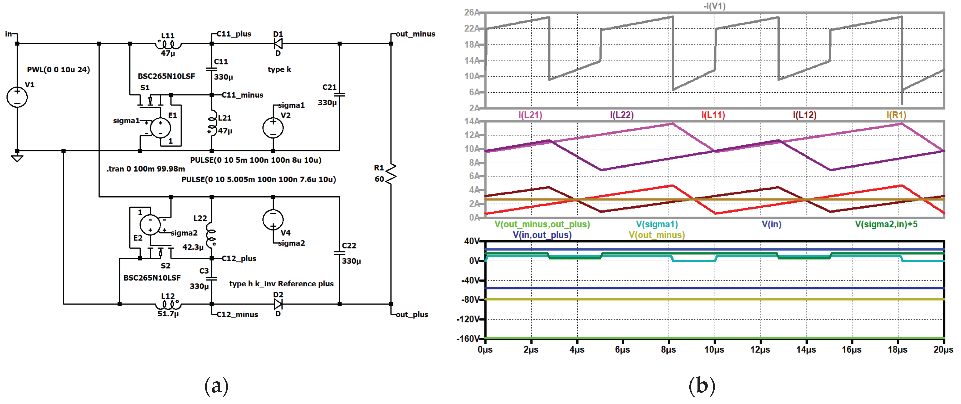
Figure 7.
Type I: (a) simulation circuit, (b) top to bottom: input current (dark violet); current through second coil of the second stage (black), current through the first coil of the second stage (grey); current through the second coil of the first stage (violet), current through the first coil of the first stage (red); input voltage (blue), control signal of the second stage (dark green, shifted), control signal of the first stage (turquoise), output voltage (green).
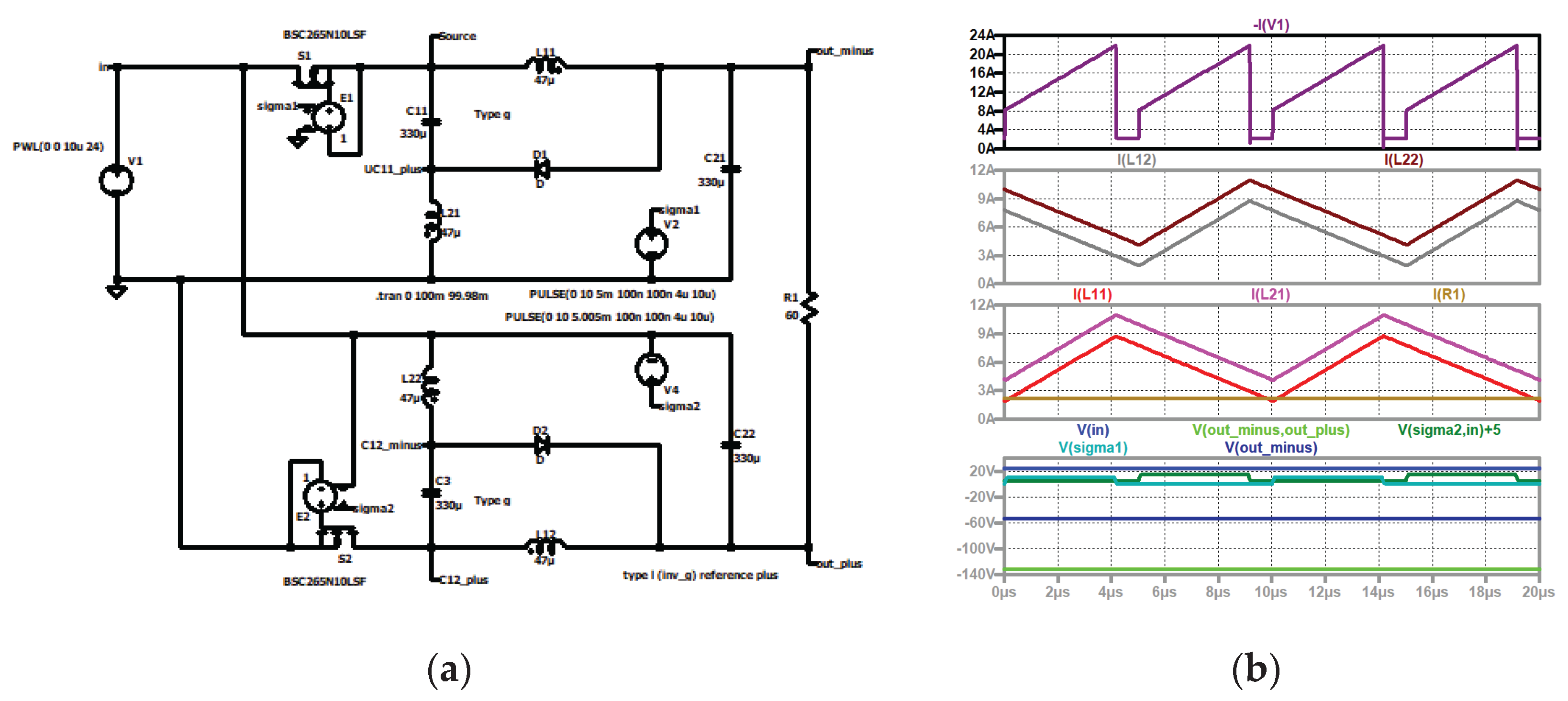
Figure 9.
Type I: simulation circuit.
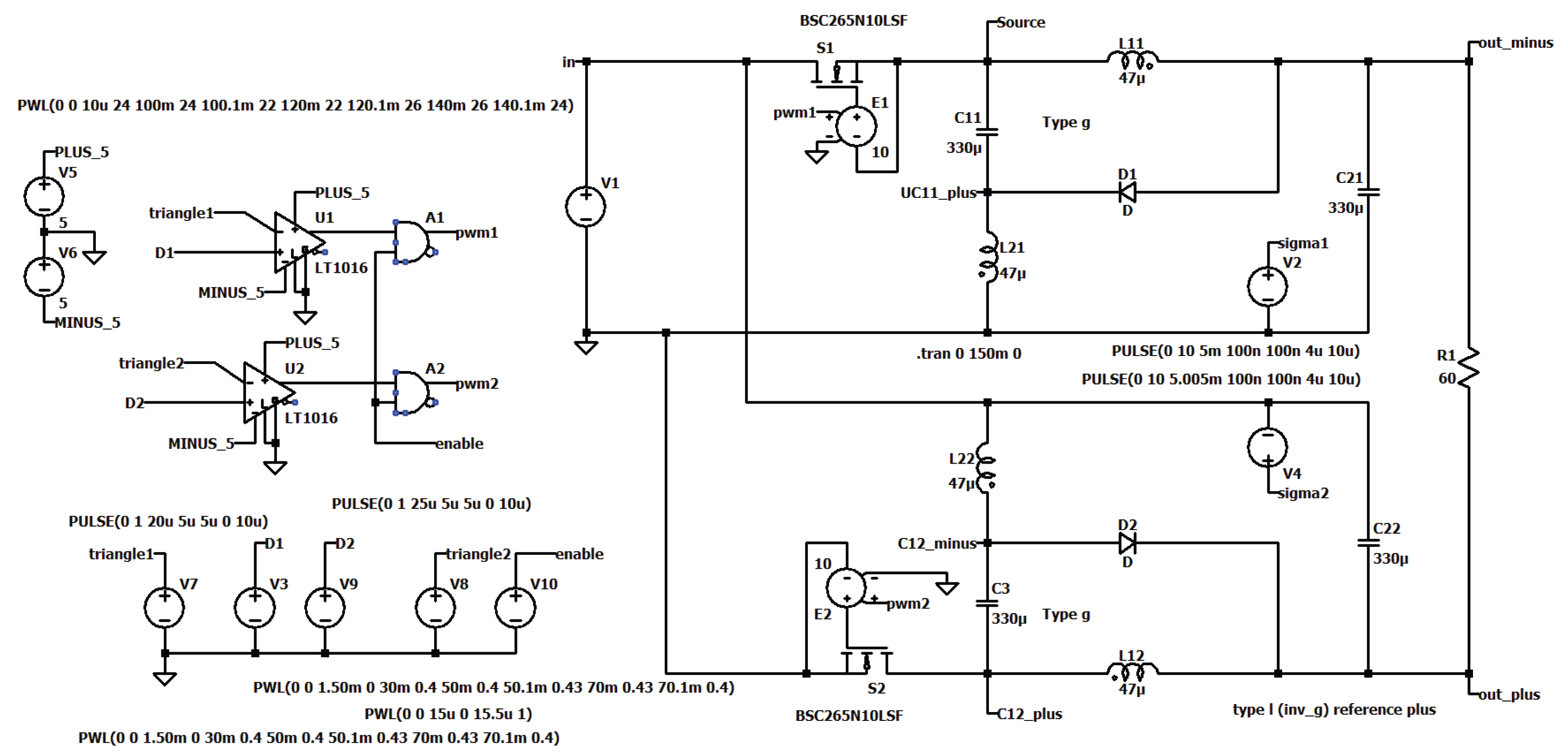
Figure 10.
Type I: start-up, duty cycle steps, input voltage steps: simulation circuit see Figure 9, top to bottom: current through the second coil of stage one (violet); current through the first coil of stage one (red); duty cycle (grey); input voltage (blue), output voltage (green).
Figure 10.
Type I: start-up, duty cycle steps, input voltage steps: simulation circuit see Figure 9, top to bottom: current through the second coil of stage one (violet); current through the first coil of stage one (red); duty cycle (grey); input voltage (blue), output voltage (green).
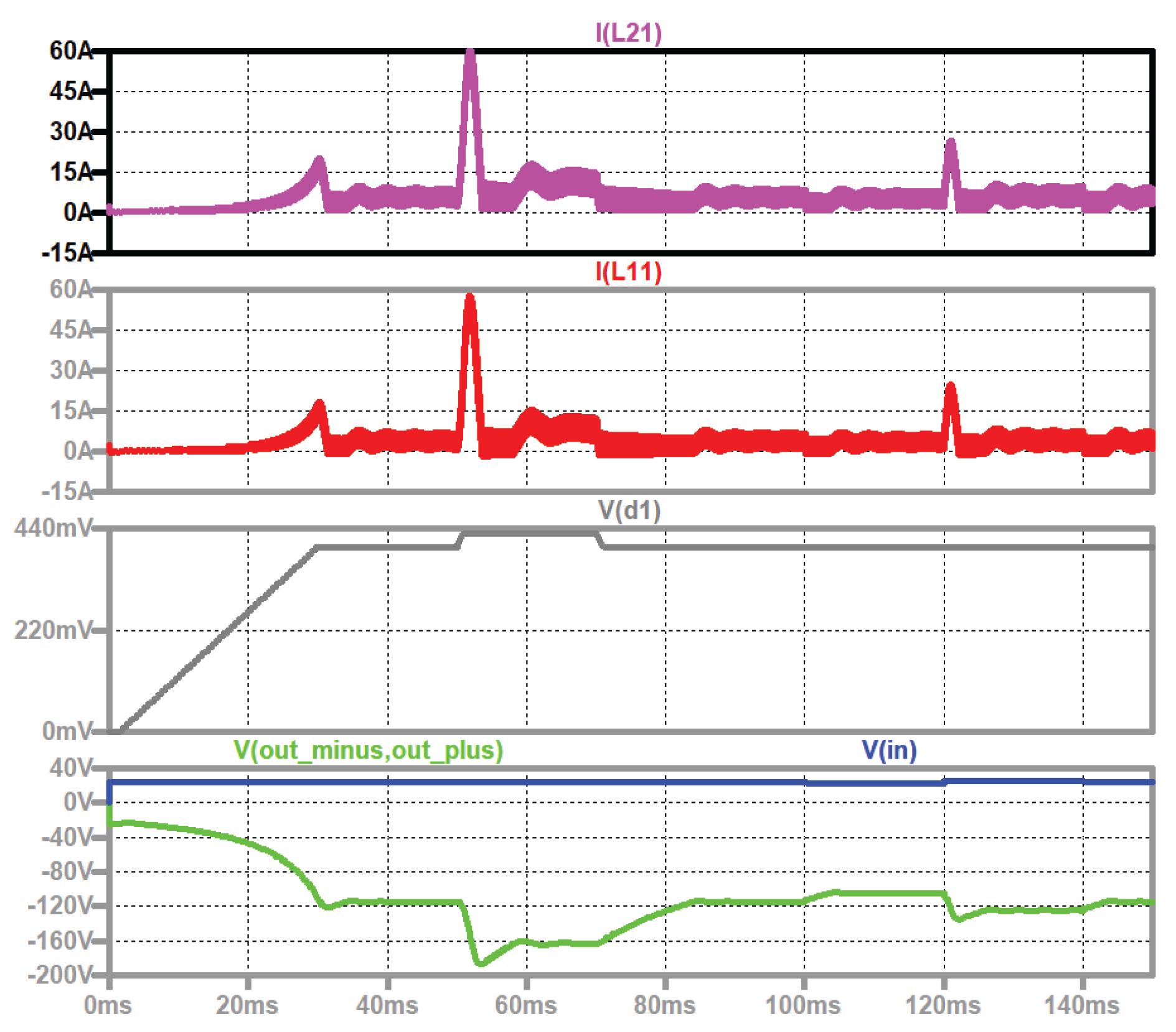
Figure 11.
Type I, start-up, duty cycle changes, input voltage steps: (a) simulation circuit; (b) top to bottom: current through the second coil of stage one (violet); current through the first coil of stage one (red); duty cycle (grey); input voltage (blue), output voltage (green).
Figure 11.
Type I, start-up, duty cycle changes, input voltage steps: (a) simulation circuit; (b) top to bottom: current through the second coil of stage one (violet); current through the first coil of stage one (red); duty cycle (grey); input voltage (blue), output voltage (green).
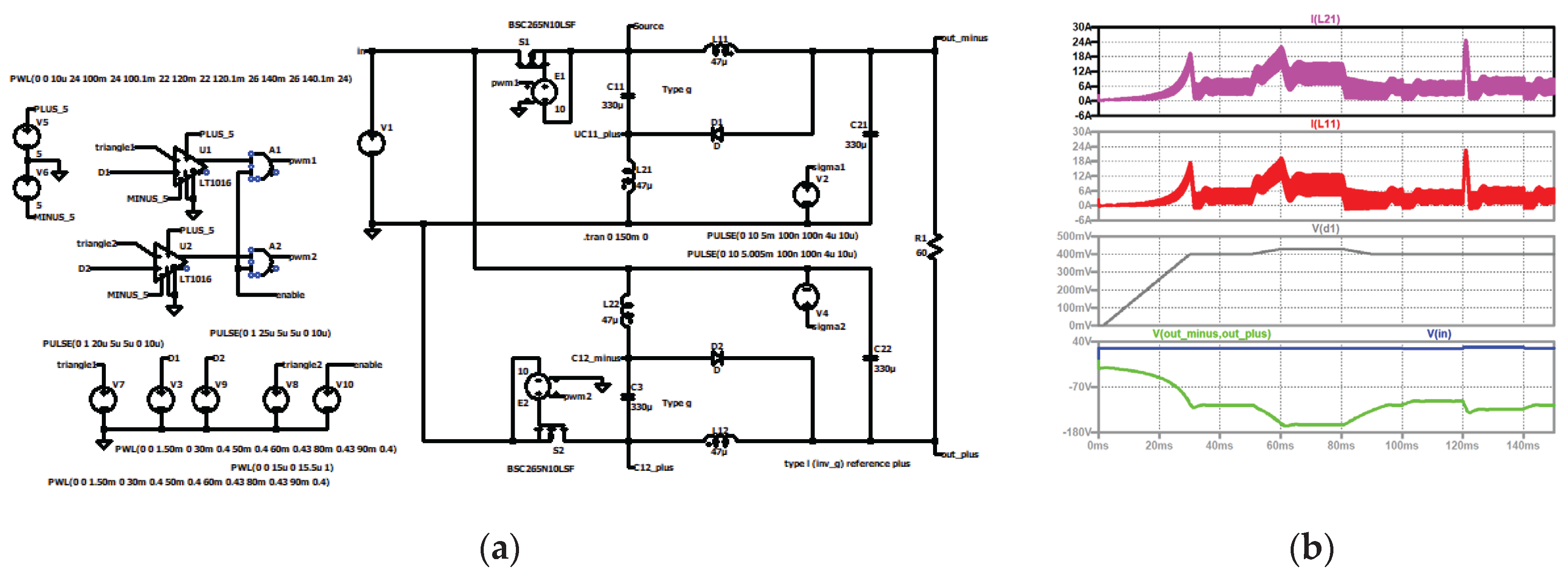
Figure 12.
Type I, simulation circuit to solve the differential matrix equation (18).
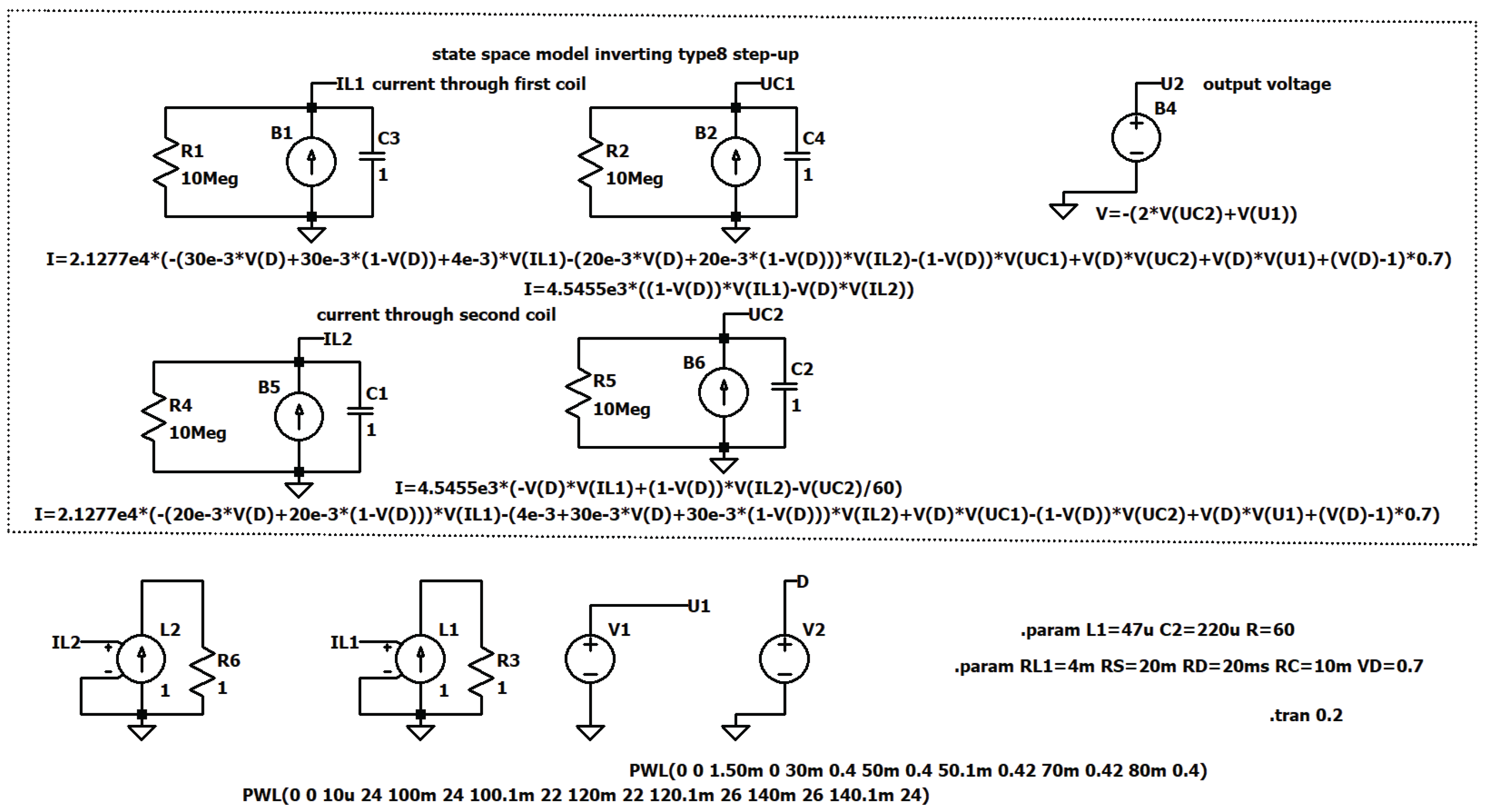
Figure 13.
Type I, simulation circuit see Figure 12, start-up, duty cycle changes, input voltage steps, top to bottom: current through the second coil of the first stage (violet), current through the first coil of the first stage (red); duty cycle (grey); input voltage (blue), output voltage (green).
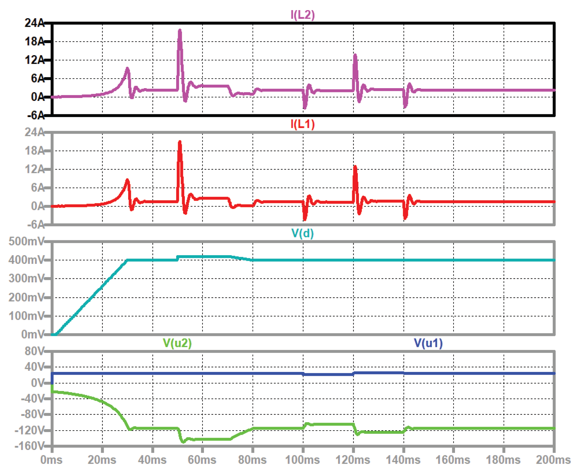
Figure 14.
Type I: (a) simulation circuit; (b) up to down: input current (dark violet); input voltage (blue), voltage across output capacitor of stage 1 (turquoise), voltage across output capacitor of stage 2 (dark green), output voltage (turquoise).
Figure 14.
Type I: (a) simulation circuit; (b) up to down: input current (dark violet); input voltage (blue), voltage across output capacitor of stage 1 (turquoise), voltage across output capacitor of stage 2 (dark green), output voltage (turquoise).
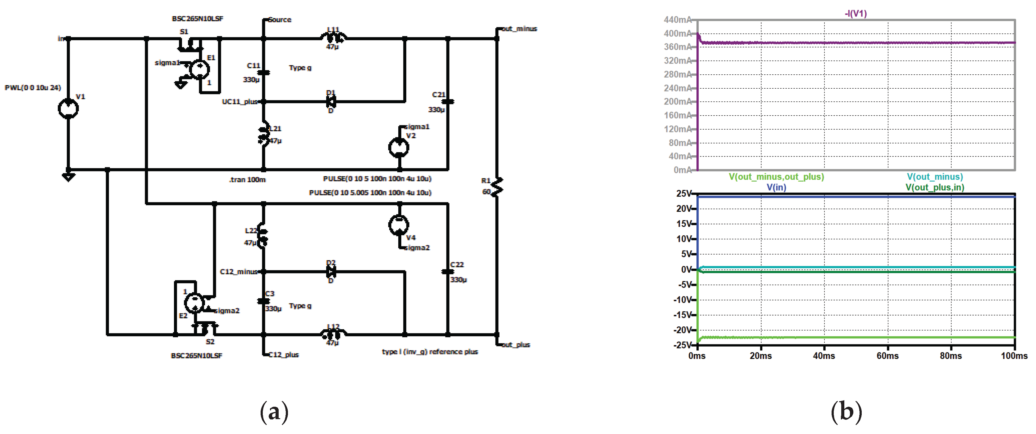
Figure 15.
Type I interleaved: (a) simulation circuit; (b) top to bottom: current through second coil of the first stage (violet), current through first coil of the first stage (red); duty cycle (grey); input voltage (blue), output voltage (green).
Figure 15.
Type I interleaved: (a) simulation circuit; (b) top to bottom: current through second coil of the first stage (violet), current through first coil of the first stage (red); duty cycle (grey); input voltage (blue), output voltage (green).
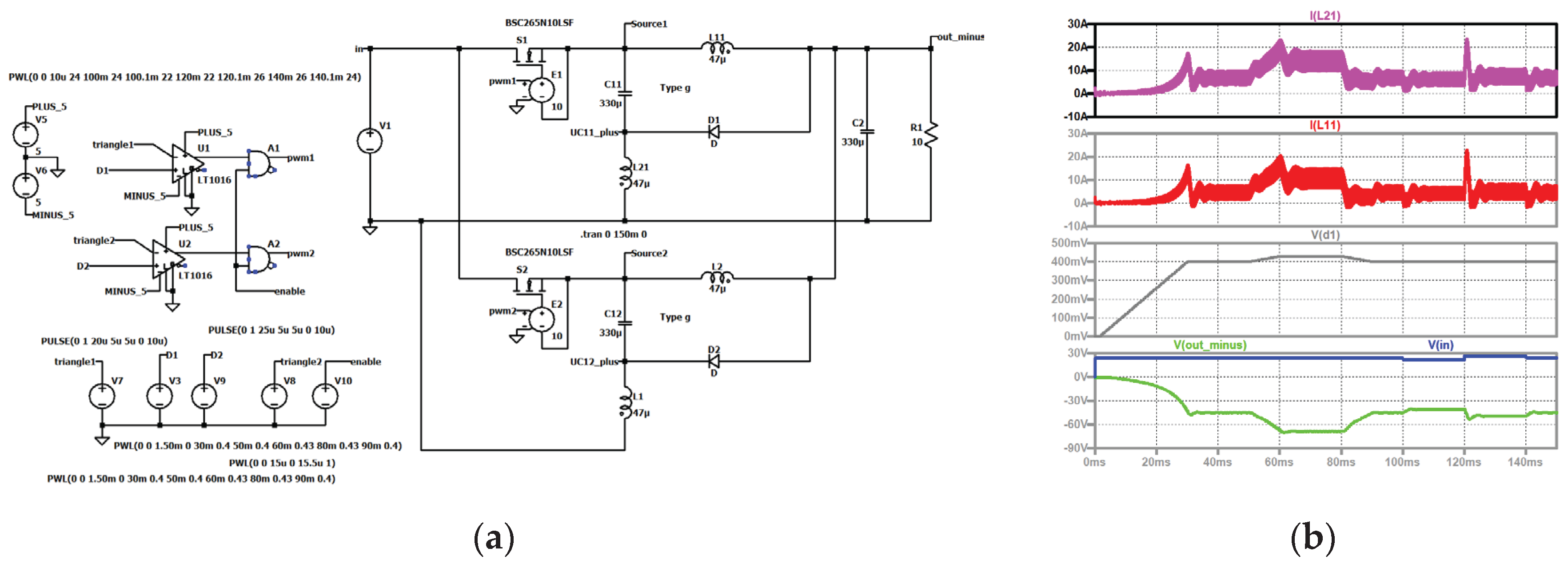
Figure 16.
type 8 interleaved: (a) in the steady state, simulation circuit, top to bottom: input current (dark violet); current through the second coil of the second stage (black), current through the first coil of the second stage (grey); current through second coil of the first stage (violet), current through the first coil of the first stage (red); input voltage (blue), control signal of the switch of the second stage (dark green, shifted), control signal of the switch of the first stage (turquoise), output voltage (green); (b) . top to bottom: current through the second coil of the first stage (violet), current through the first coil of the first stage (red); duty cycle (grey); input voltage (blue), output voltage (green).
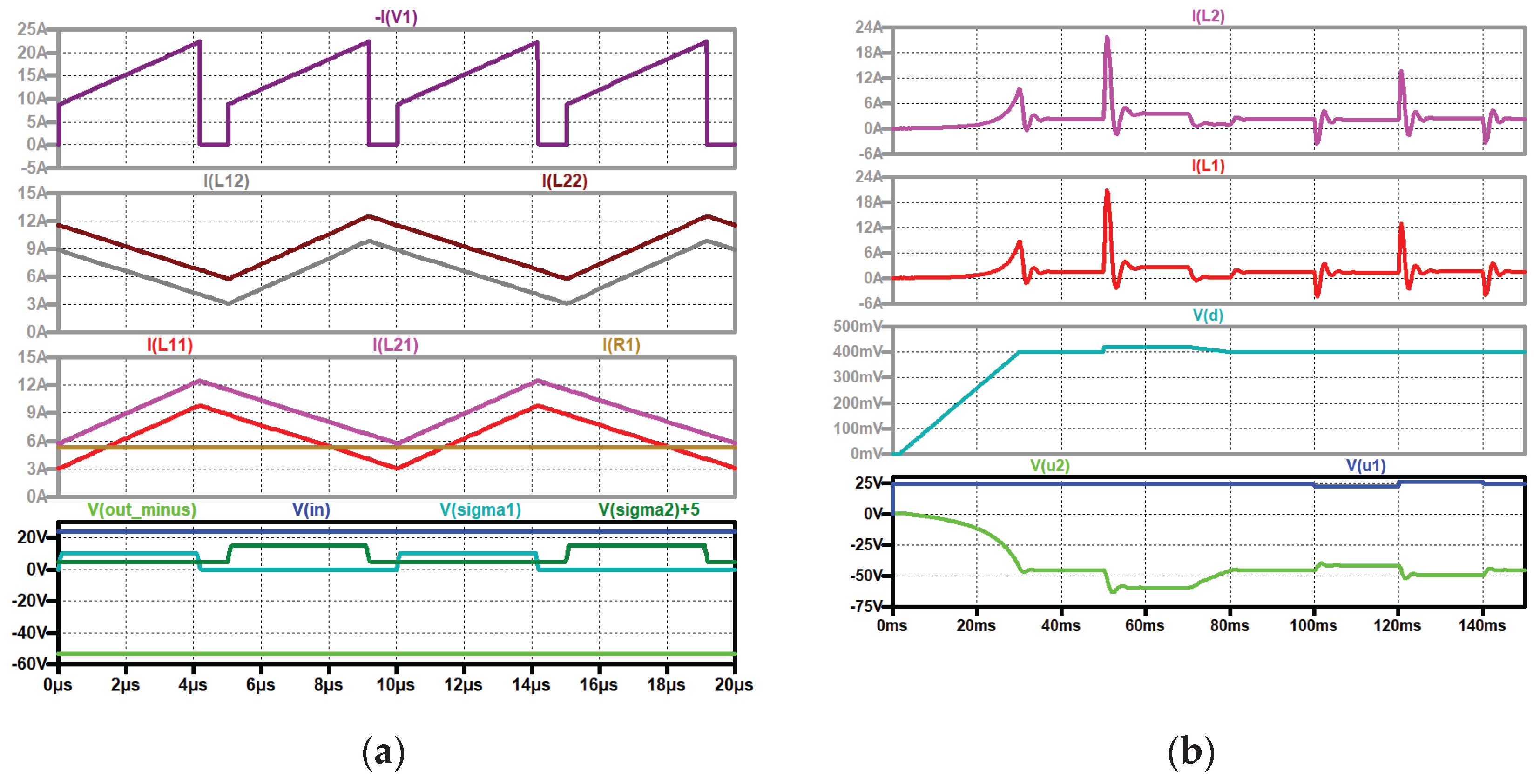
Figure 17.
Type II: circuit diagram.
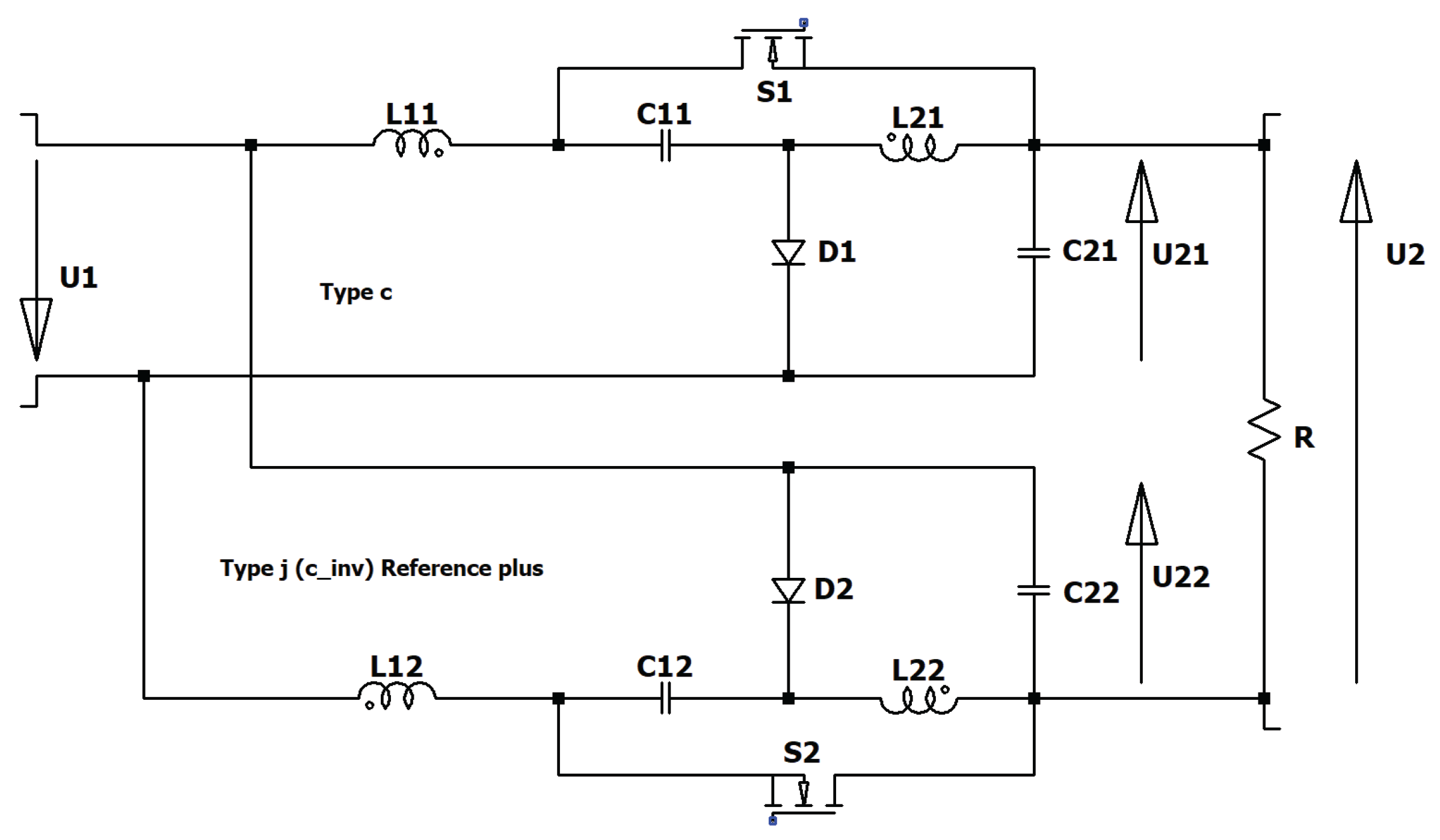
Figure 18.
Type II duty cycle 1/3: (a) simulation circuit; (b) top to bottom: current through the second coil of stage one (violet), current through the second coil of stage two (dark violet), current through the first coil of stage one (red), current through the first coil of stage two (black), load current (brown); input voltage (blue), control signal of the second switch (dark green, shifted), control signal of the first switch (turquoise), output voltage (green).
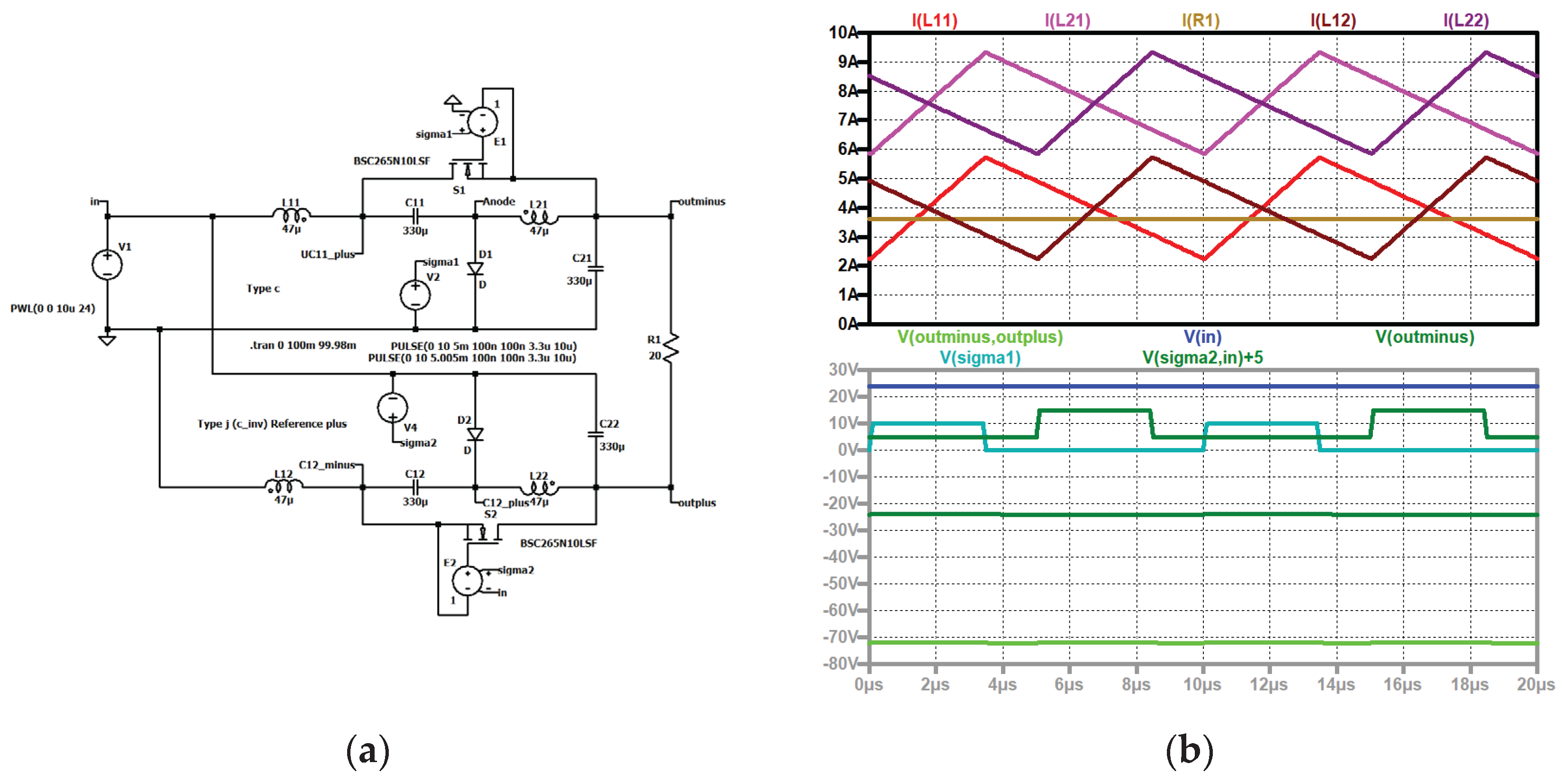
Figure 19.
Type II, dynamic simulation: (a) simulation circuit; (b) top to bottom: current through the second coil of stage one (violet); current through the first coil of the first stage (red); duty cycle (grey); input voltage (blue), output voltage of stage one, and output voltage of the complete converter.
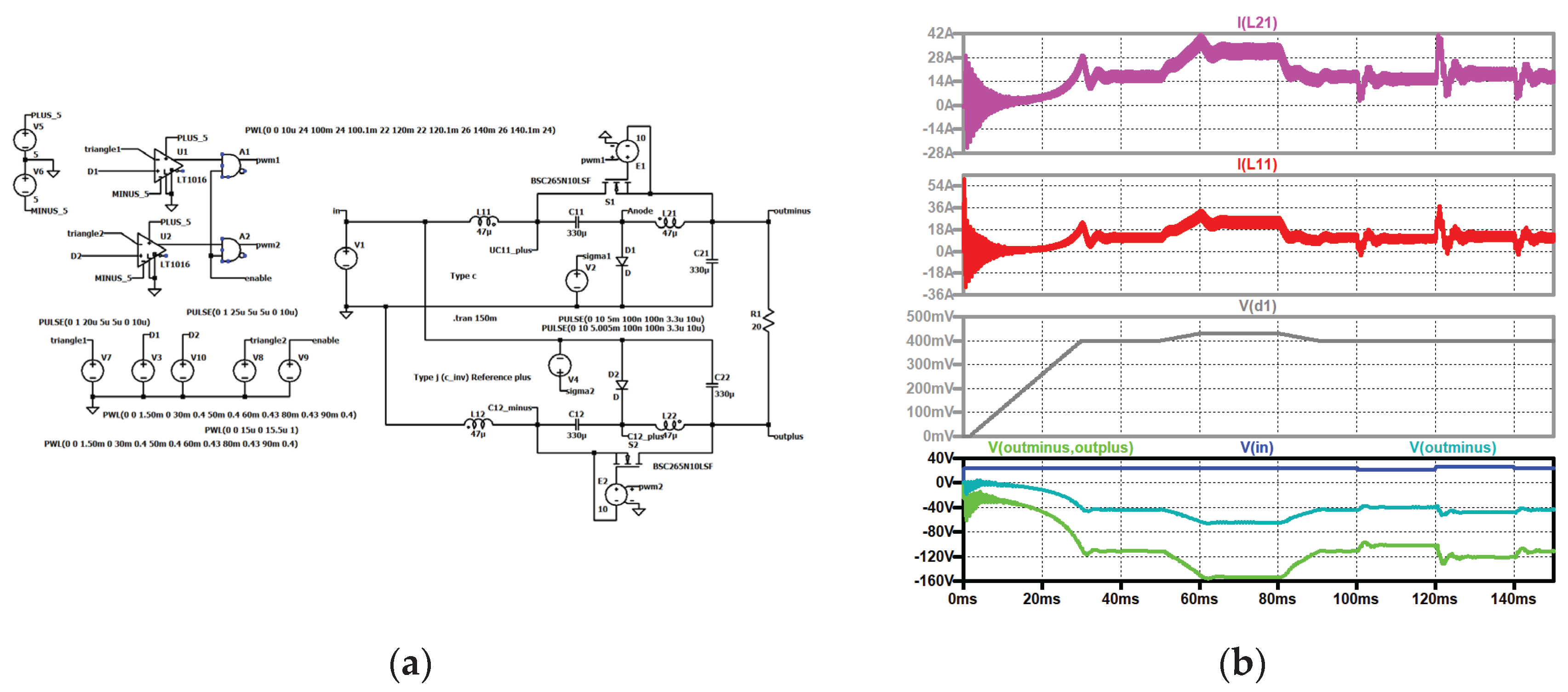
Figure 20.
Type II, inrush: (a) up to down: input current (dark violet); current through the first coil of stage 2 (violet); current through the first coil of stage 1 (red); output voltage of stage 1 (turquoise), output voltage (green), output voltage of stage 2 (dark green); (b) up to down: input current (dark violet); current through the first coil of stage 2 (violet); current through the first coil of stage 1 (red); input voltage (blue), output voltage (green), output voltage of stage 1 (turquoise), output voltage of stage 2 (dark green).
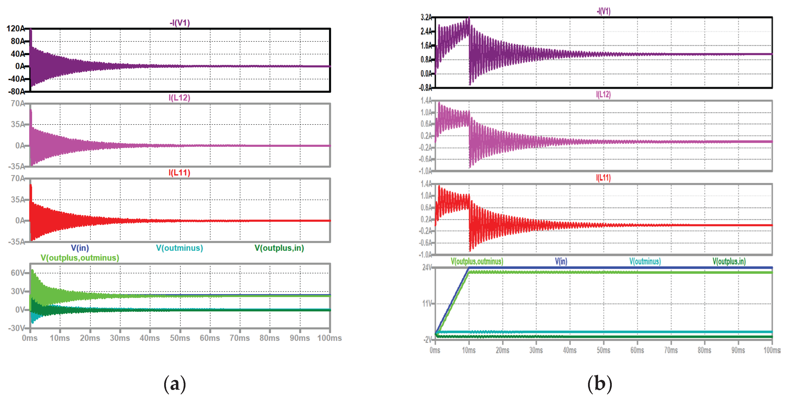
Figure 21.
Circuit diagram of the floating two-stage converter type III.
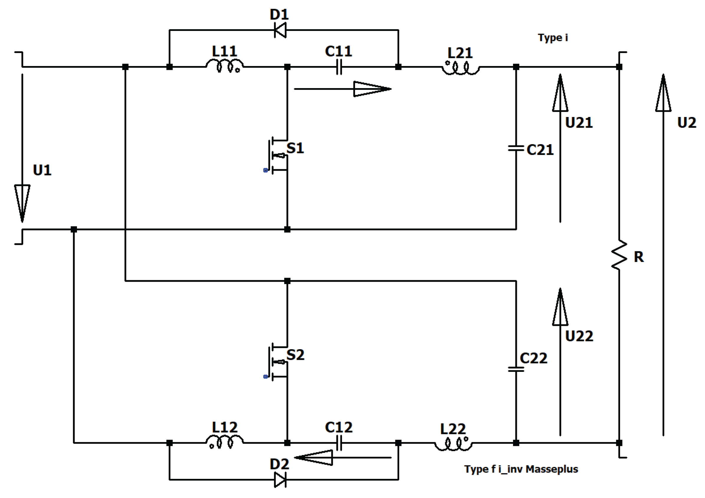
Figure 22.
type III: voltage transformation ratio of the two-stage converter (blue) and of a single stage (brown).
Figure 22.
type III: voltage transformation ratio of the two-stage converter (blue) and of a single stage (brown).
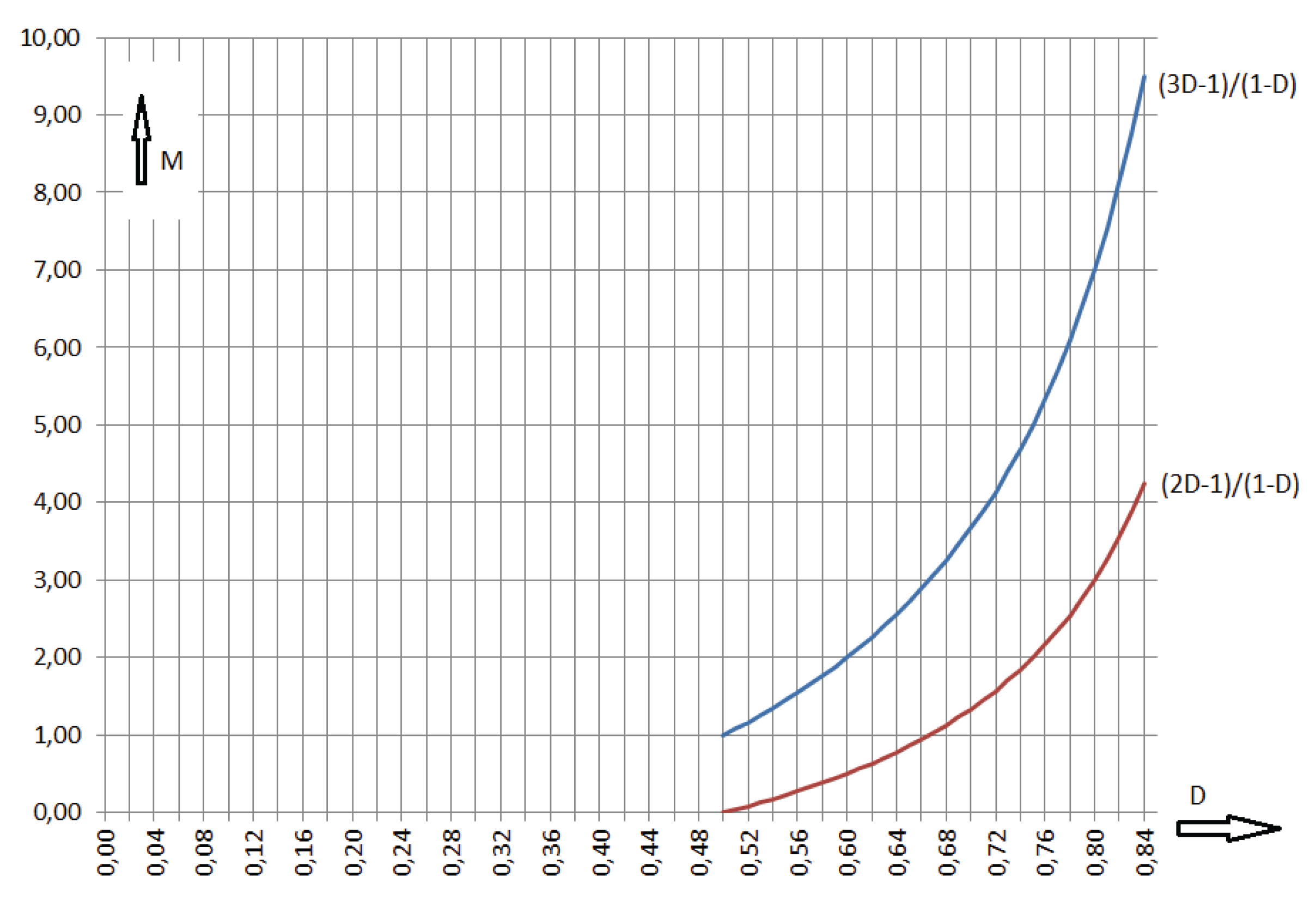
Figure 22.
type 5: equivalent circuit during M1.
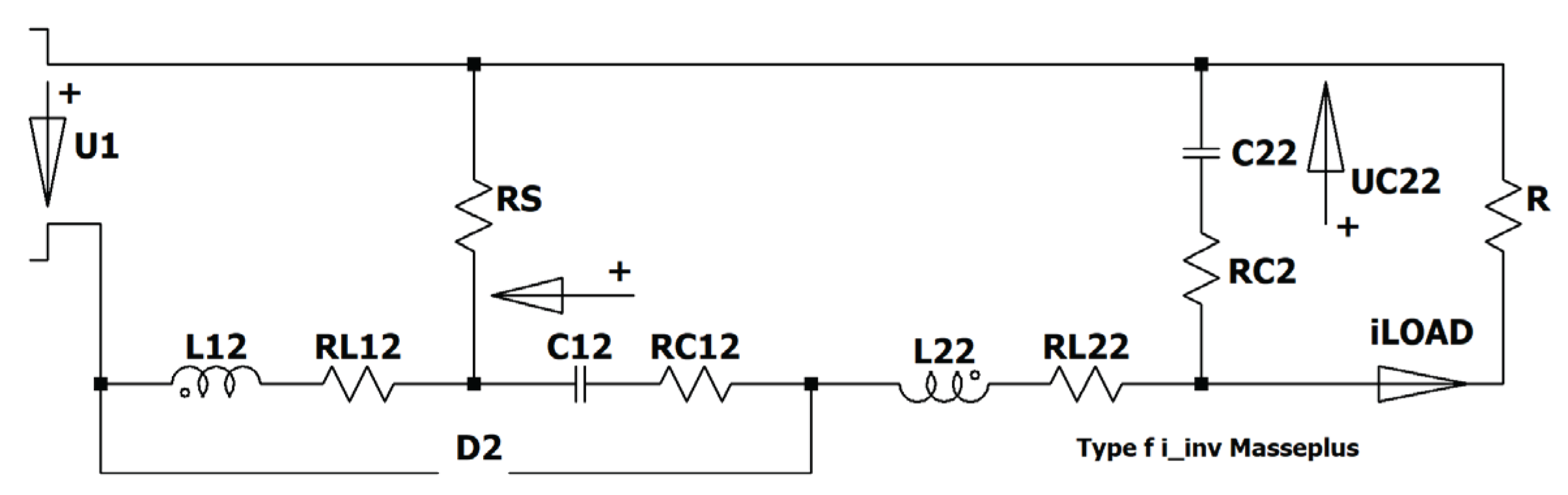
Figure 23.
Type III equivalent circuit during M2.
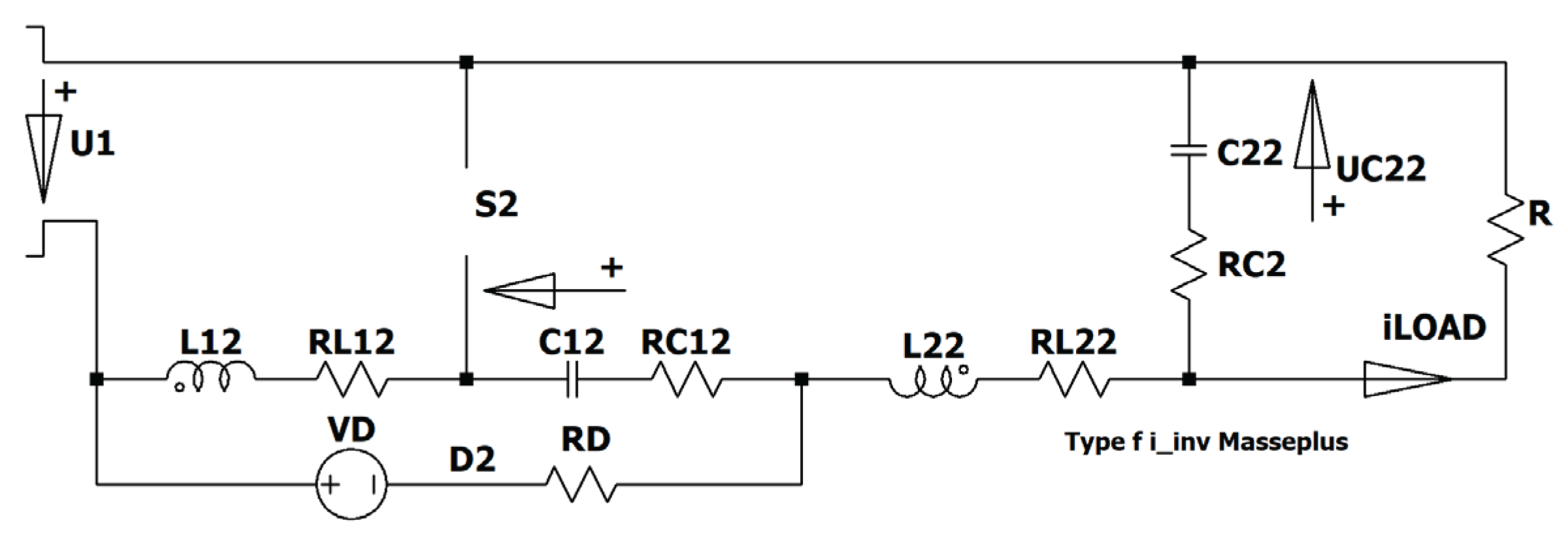
Figure 24.
Type III: (a) simulation circuit; (b), up to down: input current (dark violet); currents through the coils of stage 2 L12 (grey), L22 (light brown), load current (brown); currents through the coils of stage 1 L11 (red), L21 (violet), load current (brown); output voltage (absolute value, green), voltage across output capacitor of stage 1 (dark blue), input voltage (blue), control signal of S2 (dark green, shifted), control signal of S1 (turquoise).
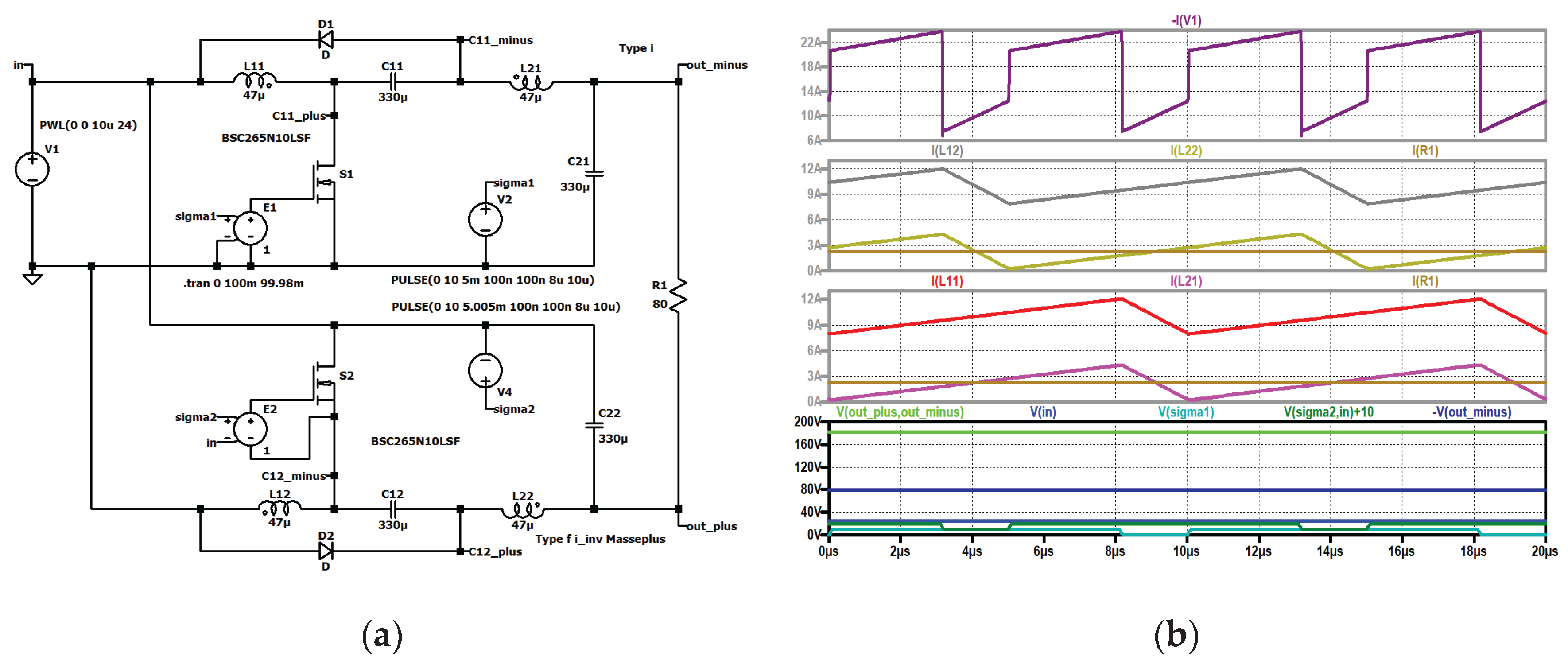
Figure 25.
Type III: (a) simulation circuit; (b) top to bottom: current through the second coil (violet); current through the first coil (red); duty cycle (grey); input voltage (blue), output voltage of stage 1 (turquoise), output voltage (green).
Figure 25.
Type III: (a) simulation circuit; (b) top to bottom: current through the second coil (violet); current through the first coil (red); duty cycle (grey); input voltage (blue), output voltage of stage 1 (turquoise), output voltage (green).
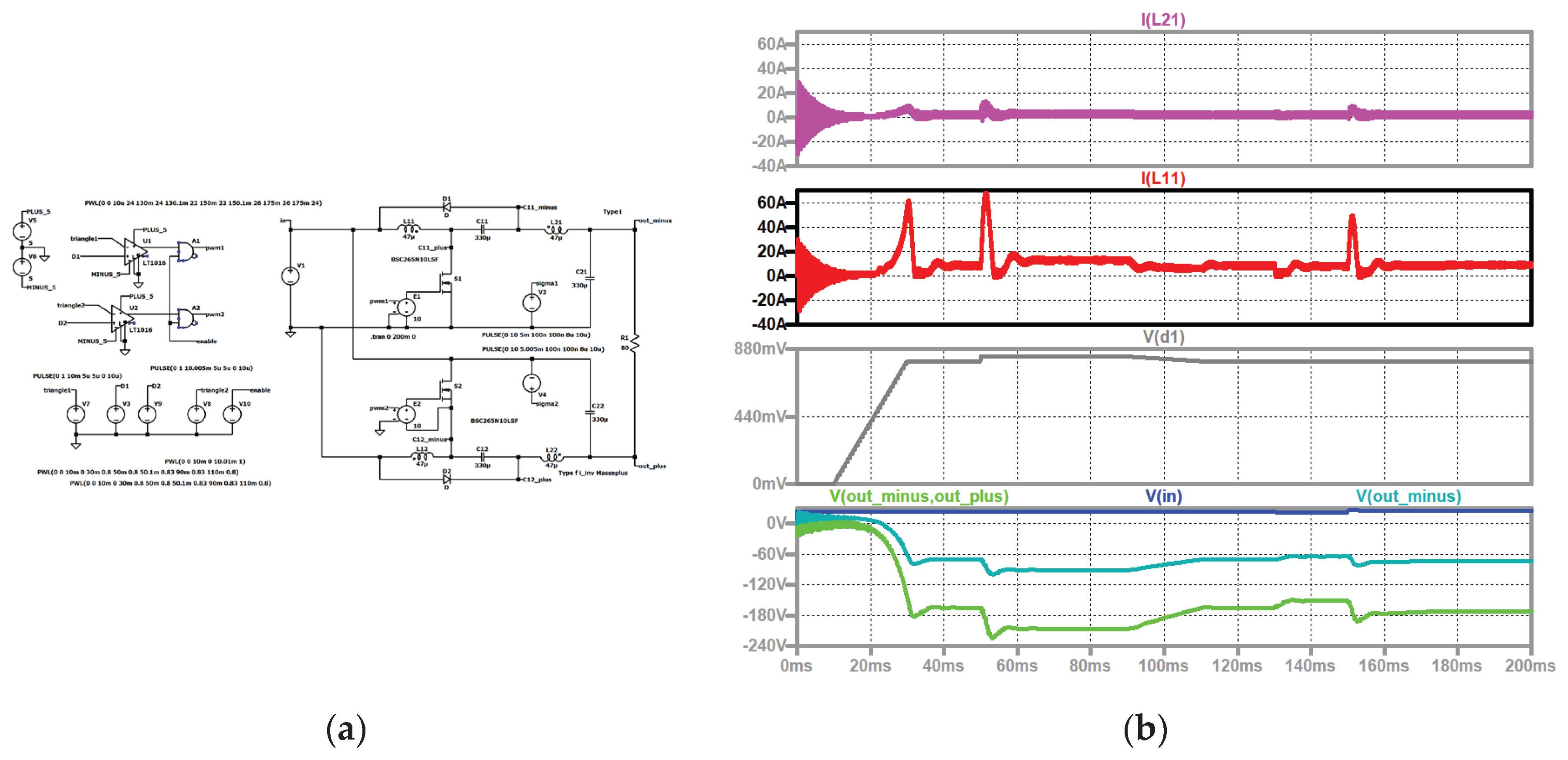
Figure 26.
Type III: (a) simulation circuit; (b) top to bottom: current through the second coil (violet); current through the first coil (red); duty cycle (grey); input voltage (blue), output voltage of stage 1 (turquoise), output voltage (green).
Figure 26.
Type III: (a) simulation circuit; (b) top to bottom: current through the second coil (violet); current through the first coil (red); duty cycle (grey); input voltage (blue), output voltage of stage 1 (turquoise), output voltage (green).
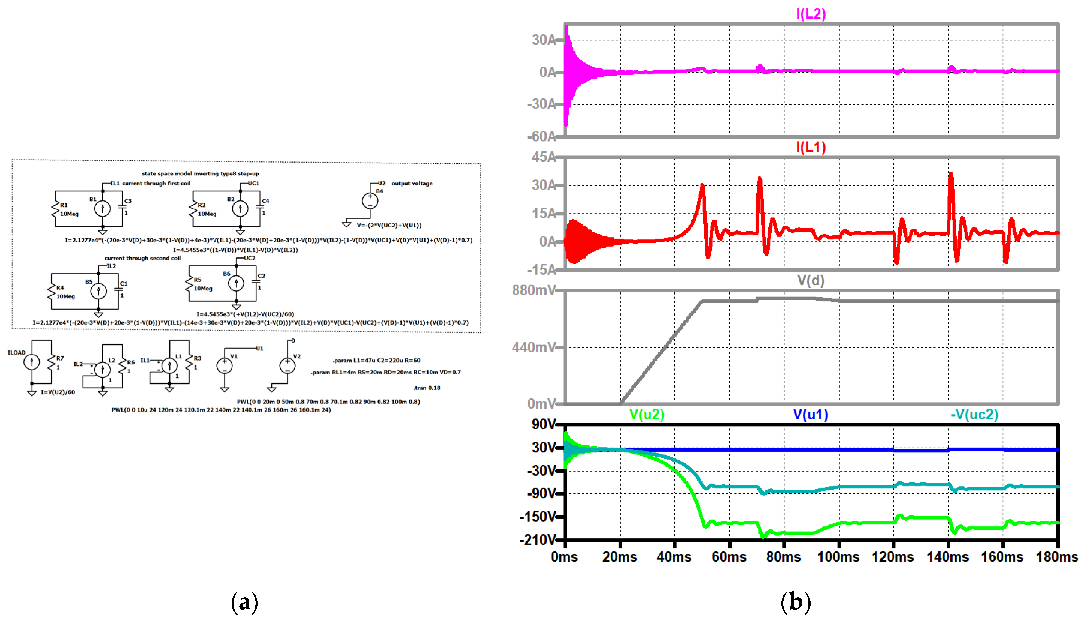
Figure 27.
Type III, with input voltage-ramp: (a) simulation circuit; (b) up to down: input current (dark violet); input voltage (blue), output voltage (green), voltages across the output of the stages stage 1 (turquoise), stage 2(dark green).
Figure 27.
Type III, with input voltage-ramp: (a) simulation circuit; (b) up to down: input current (dark violet); input voltage (blue), output voltage (green), voltages across the output of the stages stage 1 (turquoise), stage 2(dark green).
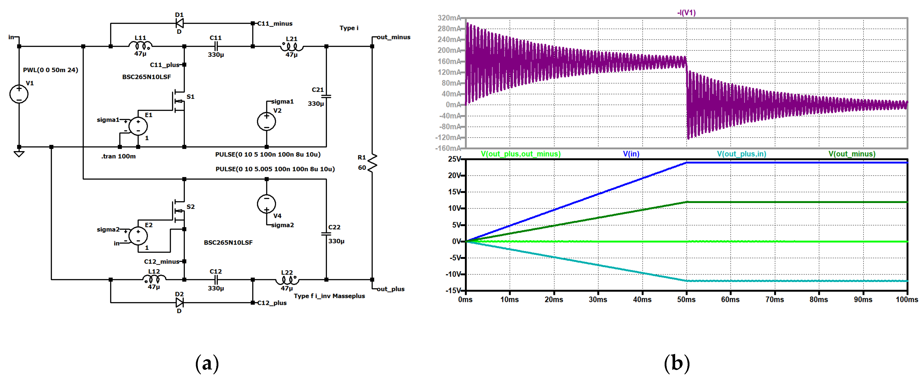
Figure 28.
Circuit diagram type IV.
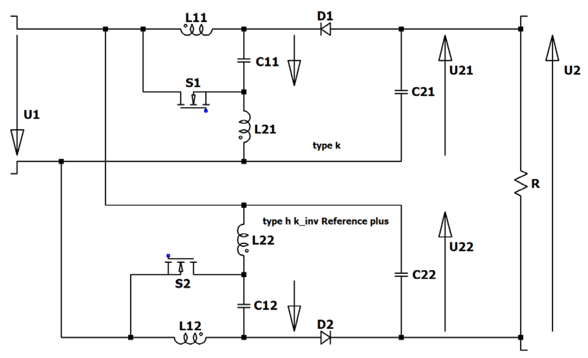
Figure 29.
Type IV steady state: (a) simulation circuit, (b) top to bottom: input current (grey); current through the second coil of stage one (violet), current through the second coil of stage two (dark violet), current through the first coil of stage one (red), current through the first coil of stage two (black), load current (brown); input voltage (blue), control signal of the second switch (dark green, shifted), control signal of the first switch (turquoise), output voltage (green).
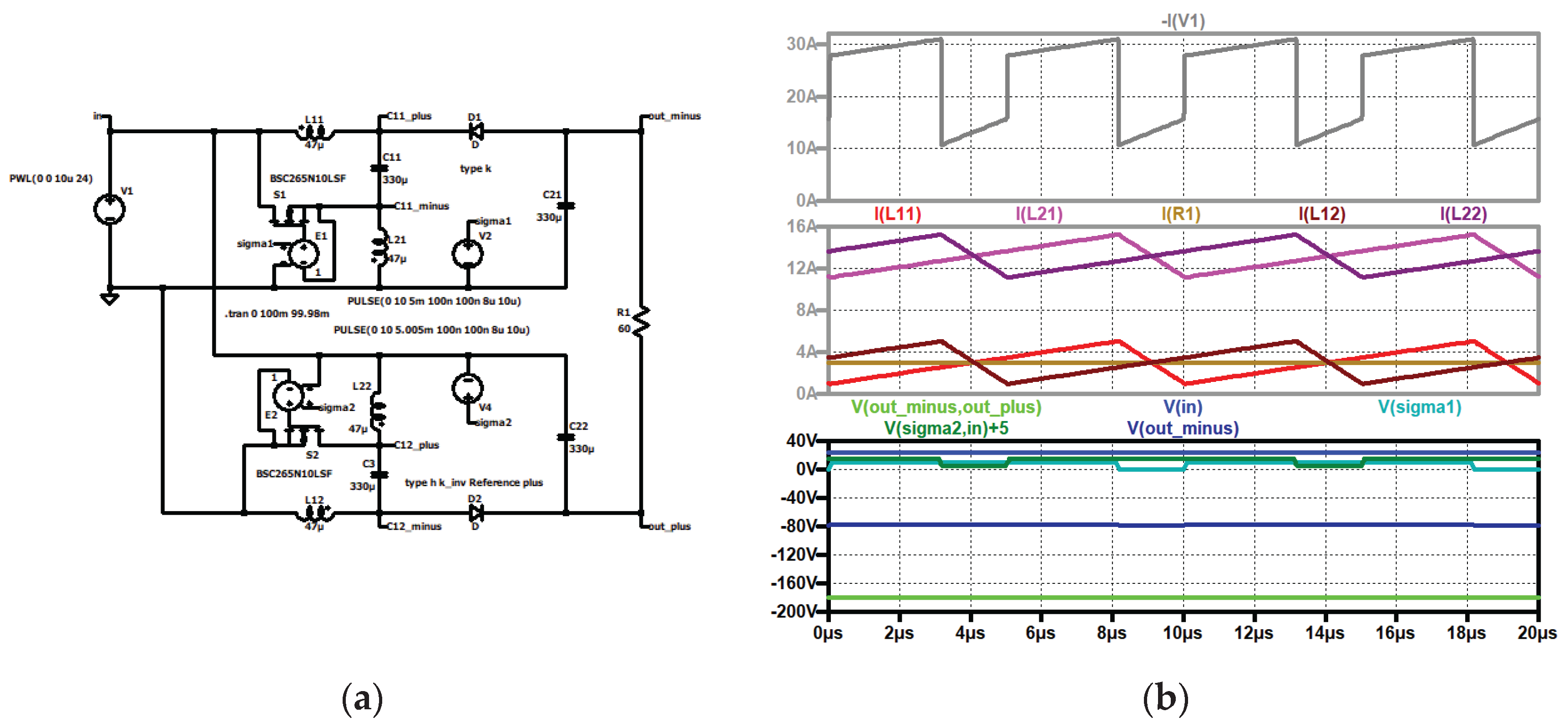
Figure 30.
Type IV: (a) simulation circuit; (b) top to bottom: current through the second coil (violet); current through the first coil (red); duty cycle (grey); input voltage (blue), output voltage (green).
Figure 30.
Type IV: (a) simulation circuit; (b) top to bottom: current through the second coil (violet); current through the first coil (red); duty cycle (grey); input voltage (blue), output voltage (green).
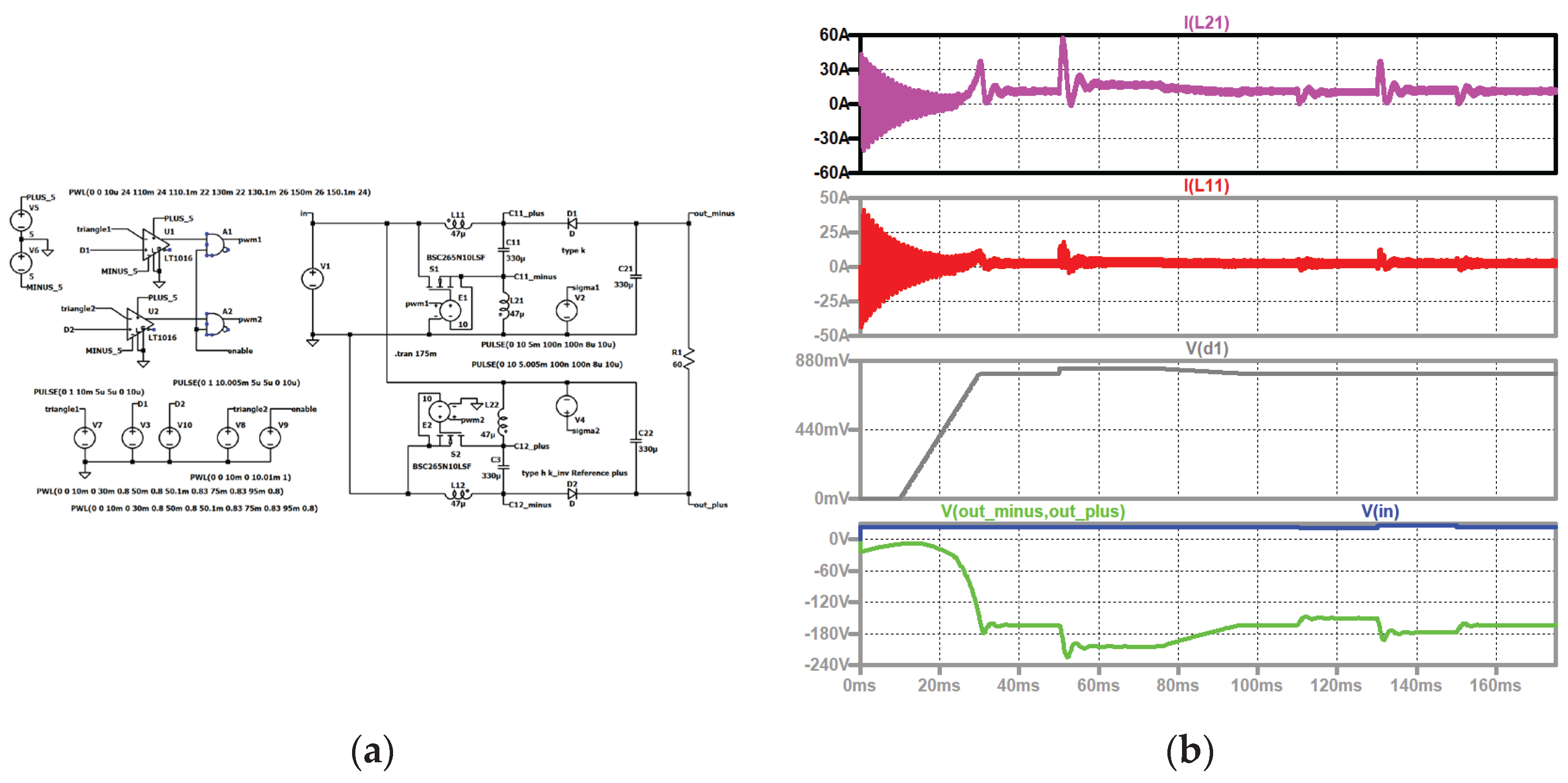
Figure 31.
Type IV: (a) simulation circuit; (b) top to bottom: current through the second coil (violet); current through the first coil (red); duty cycle (grey); input voltage (blue), output voltage of one stage (turquoise), output voltage (green).
Figure 31.
Type IV: (a) simulation circuit; (b) top to bottom: current through the second coil (violet); current through the first coil (red); duty cycle (grey); input voltage (blue), output voltage of one stage (turquoise), output voltage (green).
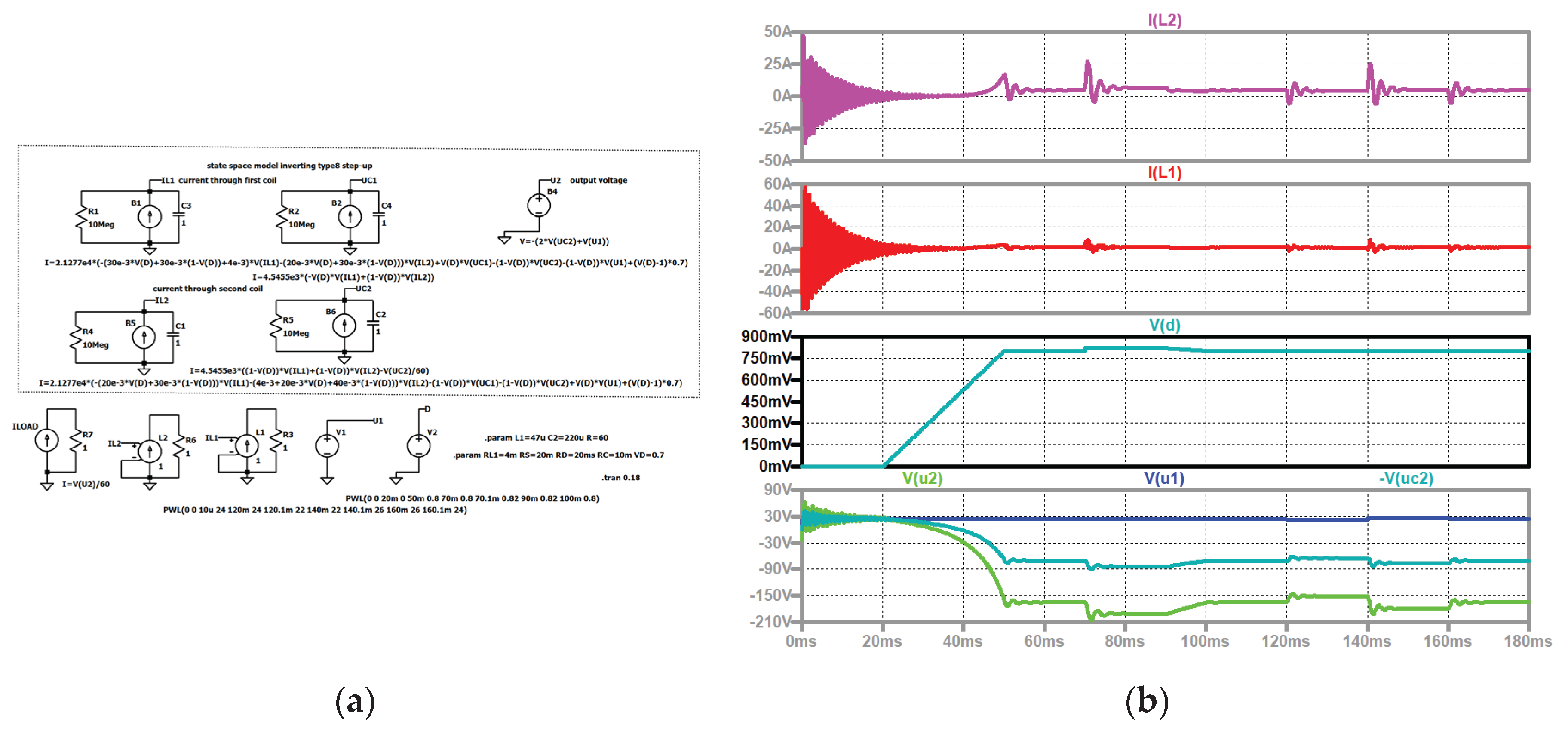
Figure 32.
Type IV, Bode diagram: (a) simulation circuit; (b) connection between the output voltage of one stage in dependence on the duty cycle.
Figure 32.
Type IV, Bode diagram: (a) simulation circuit; (b) connection between the output voltage of one stage in dependence on the duty cycle.
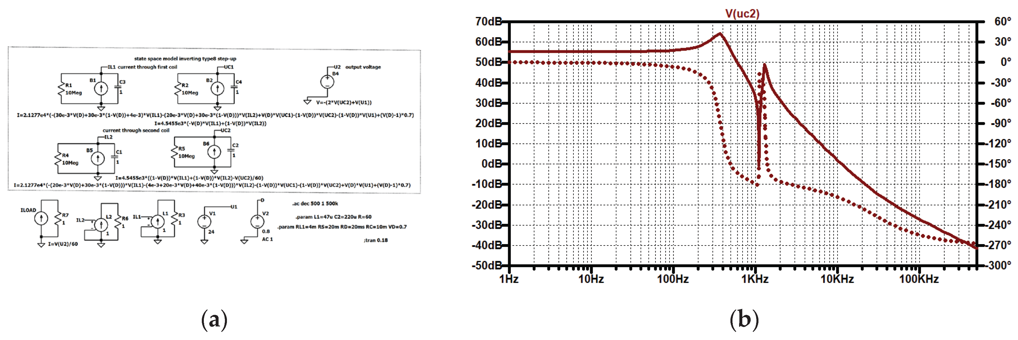
Figure 33.
Avoiding the inrush with a damping resistor, type IV: (a) simulation circuit; (b) top to bottom: input voltage (blue), output voltage (green); input current (dark violet).
Figure 33.
Avoiding the inrush with a damping resistor, type IV: (a) simulation circuit; (b) top to bottom: input voltage (blue), output voltage (green); input current (dark violet).
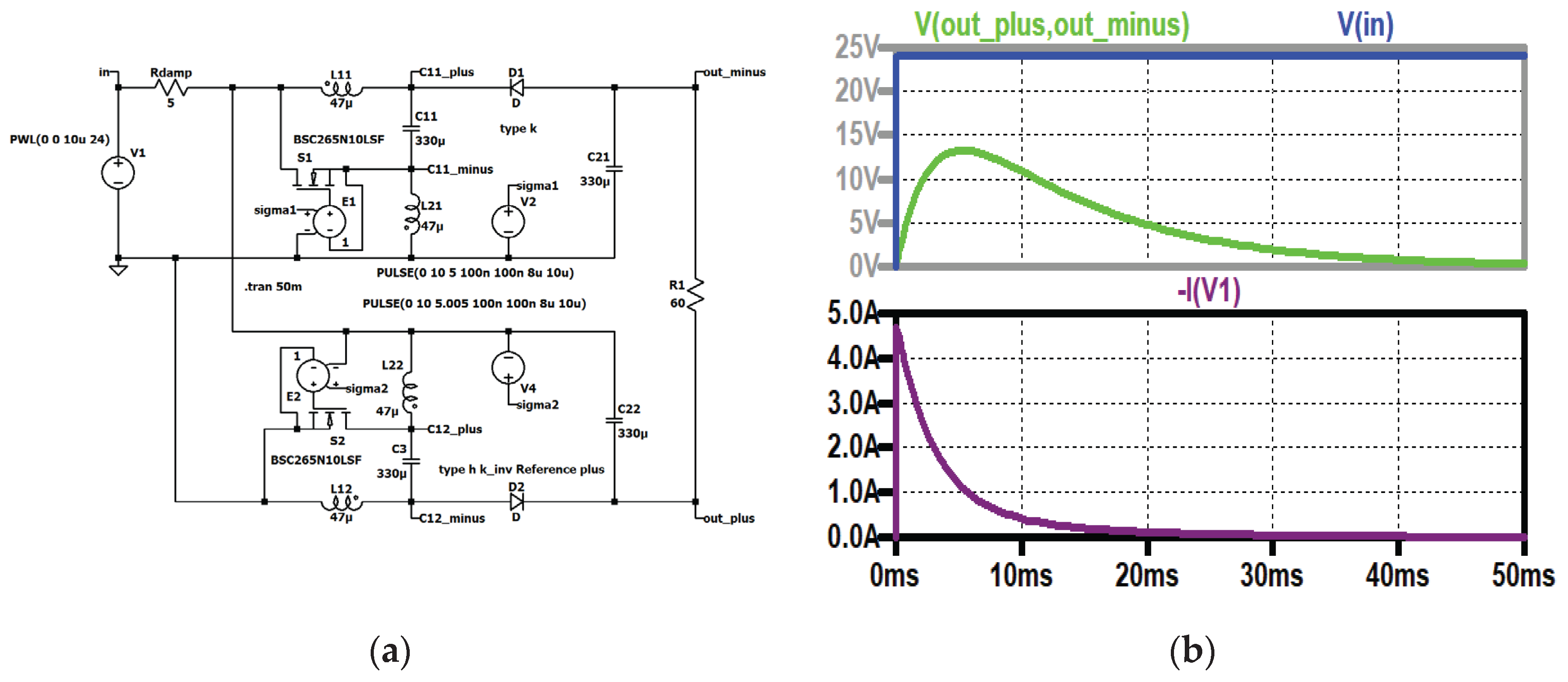
Figure 34.
Avoiding the inrush with a ramp, type IV: (a) simulation circuit; (b) top to bottom: input voltage (blue), output voltage (green); input current (dark violet).
Figure 34.
Avoiding the inrush with a ramp, type IV: (a) simulation circuit; (b) top to bottom: input voltage (blue), output voltage (green); input current (dark violet).
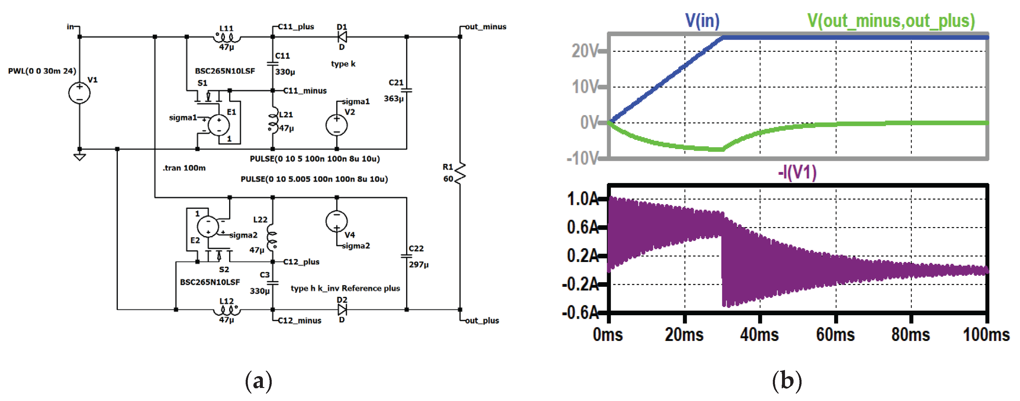
Figure 35.
Type IV steady state with tolerances of the coils, (a) simulation circuit, (b) top to bottom: input current (grey); current through the second coil of stage one (violet), current through the second coil of stage two (dark violet), current through the first coil of stage one (red), current through the first coil of stage two (black), load current (brown); input voltage (blue), control signal of the second switch (dark green, shifted), control signal of the first switch (turquoise), output voltage (green).
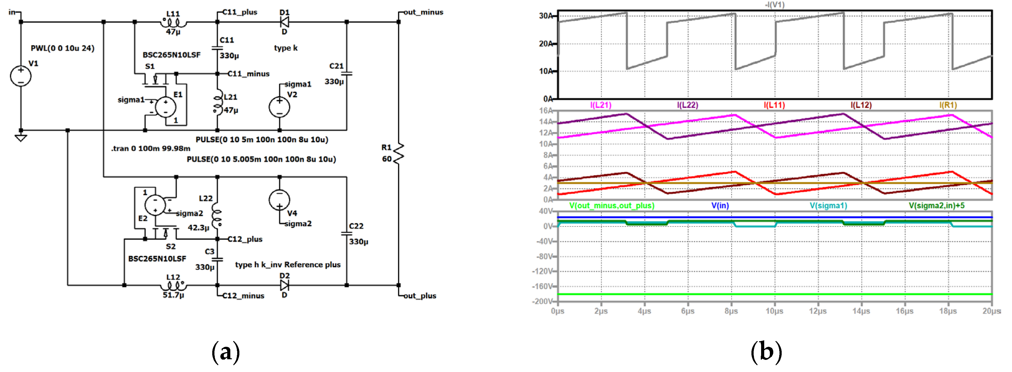
Figure 36.
Type IV steady state with tolerances of the coils by plus/minus 10 % and the duty cycles of the two stages differ by 5 %, (a) simulation circuit, (b) top to bottom: input current (grey); current through the second coil of stage one (violet), current through the second coil of stage two (dark violet), current through the first coil of stage one (red), current through the first coil of stage two (black), load current (brown); input voltage (blue), control signal of the second switch (dark green, shifted), control signal of the first switch (turquoise), output voltage of stage two (dark blue), output voltage of stage one (light brown), output voltage (green).
Disclaimer/Publisher’s Note: The statements, opinions and data contained in all publications are solely those of the individual author(s) and contributor(s) and not of MDPI and/or the editor(s). MDPI and/or the editor(s) disclaim responsibility for any injury to people or property resulting from any ideas, methods, instructions or products referred to in the content. |
© 2025 by the authors. Licensee MDPI, Basel, Switzerland. This article is an open access article distributed under the terms and conditions of the Creative Commons Attribution (CC BY) license (http://creativecommons.org/licenses/by/4.0/).
Copyright: This open access article is published under a Creative Commons CC BY 4.0 license, which permit the free download, distribution, and reuse, provided that the author and preprint are cited in any reuse.


