
Submitted:
05 November 2025
Posted:
12 November 2025
You are already at the latest version
Abstract
A new generation of fluorescent diamond nanoparticles synthesized from hydrocarbons at high pressure appear to be promising for the design of efficient single-photon diamond sources and nanometer-sized optical sensors. A characteristic feature of such nanodiamonds (ND) is the termination of their surface with hydrogen. This hydrogen induces the formation of free holes at the diamond surface, thereby affecting the charge state of nearby fluorescent centers. In this study, the effect of the H-terminated ND surface on negatively charged silicon-vacancy (SiV-) fluorescence as a function of the ND size was investigated. Diamond nanoparticles of various sizes in the 50-300 nm range were analyzed before and after H desorption from their surface. It was shown that a significant increase in SiV- fluorescence (>50%) upon hydrogen removal starts for particles smaller than 100 nm. Based on the measured dependence of the SiV fluorescence intensities on the ND sizes, the effective thickness of the diamond surface layer, within which charge neutralization of SiV- centers occurs under the hydrogen influence, was determined to be 6 nm.
Keywords:
nanodiamond
; high-pressure synthesis
; silicon-vacancy center
; fluorescence
; H-terminated surface
1. Introduction
A new generation of fluorescent nanodiamonds (NDs) synthesized from various hydrocarbons at high pressure and high temperature (HPHT) is attracting increasing attention from researchers developing single-photon sources (SPS) and optical nanosensors. The synthesis of such diamond nanoparticles is typically carried out at a pressure of 7–9 GPa in the temperature range of 1000–1700 0C. The feasibility of creating efficient SPSs based on these HPHT NDs containing individual fluorescent nitrogen-vacancy (NV) [1,2,3], silicon-vacancy (SiV) [3,4,5], and germanium-vacancy (GeV) [6] centers has been demonstrated. NDs containing large ensembles of SiV centers have also been successfully employed as ultralocal temperature nanosensors in biological environments [7,8,9,10]. The possibility of controlled formation of SiV centers in such NDs was recently shown [11]. For practical applications of fluorescent HPHT NDs, it is crucial to synthesize them with high structural and phase purity, free of residual graphitic inclusions, and to minimize the potential negative influence of the surface on their fluorescence intensity [12]. A characteristic feature of NDs synthesized from hydrocarbons is their hydrogen-terminated surface, rich in surface CHx functional groups formed during the HPHT growth process [13,14]. Hydrogen termination induces the formation of a near-surface hole layer in diamond [15]. The most common fluorescent centers in diamond, negatively charged NV⁻, SiV⁻, and GeV⁻, can lose their excess electrons near the surface due to recombination with these holes, converting to neutral charge states. This results in quenching the center's fluorescence [16]. The influence of a hydrogen-terminated surface on the fluorescence intensity of HPHT diamond nanoparticles synthesized from hydrocarbons has not yet been studied in detail. Here, we present a systematic investigation of this effect by electron-beam-induced hydrogen desorption from the surface of SiV-fluorescent HPHT NDs, focusing on the size-dependent SiV emission.
2. Materials and Methods
The SiV-fluorescent NDs under study were synthesized by HPHT technique from a mixture of adamantane (C10H16, Sigma-Aldrich, St. Louis, MO, USA, 99% purity), detonation NDs (DND, Adamas Nanotechnologies Inc., Raleigh, NC, USA, average sizes 3–4 nm), containing ≈1% nitrogen impurity, and tetrakis(trimethylsilyl)silane (С12H36Si5, Sigma-Aldrich, St. Louis, MO, USA, >97%). The mixture was compressed to ≈7.5 GPa in a high-pressure chamber of the “toroid” type [17] and heated to 1350–1450 °C for 20 s. The adamantane/DND weight ratio was 25:1, and the Si/C atomic ratio was 1% in the initial growth mixture. A more detailed description of the HPHT synthesis procedure was given elsewhere [11]. Additionally, an ND sample was synthesized from a pure chloroadamantane (C10H15Cl, 98%) under ≈7.5 GPa, ≈1350 °C. The sample was used to confirm effective hydrogen desorption from the diamond surface under electron irradiation. For this purpose, the intensities of CHx vibrational modes in the Raman spectra of the sample were measured before and after electron irradiation. Unlike the SiV-containing sample, this “reference” sample facilitates the detection of the Raman CHx band due to the small average size of its diamond particles (<50 nm) and the absence of fluorescence lines associated with donor-acceptor recombination [18], which could hinder observation of the CHx Raman band. A pre-characterization of the synthesized ND sample in a Scanning Electron Microscope (SEM) JEOL 7001F, Japan revealed the ND size distribution predominantly in the range 50-300 nm for the main sample, and 30-50 nm for the “reference” sample. We employed an electron beam of the same microscope to remove surface-bound hydrogen from ND surfaces.
Micro-Raman spectroscopy and confocal laser reflectance imaging were performed using the multifunctional microscope (NTEGRA Spectra II, NT-MDT, Russia). For the Raman measurements a continuous-wave 532-nm laser was used. The spectral resolution was ≈0.5 cm−1. Each Raman spectrum was accumulated over 180 sec. During spectral acquisitions, the laser power at the sample was kept below 0.1 mW to avoid laser-induced ND heating. The confocal pinhole and objective optics conferred a diffraction-limited lateral spatial resolution of approximately 200 nm for both Raman spectrum and reflectance imaging. The confocal laser reflectance maps were recorded by a scanning the sample, which yielded high-contrast optical images of the NDs on a silicon substrate.
A custom-built confocal microscope was used for the photoluminescence (PL) characterization of the synthesized SiV-NDs. It is equipped with a high-numerical-aperture objective (Olympus 100×, NA = 0.95) and a piezoelectric translation stage (piezosystem jena TRITOR 100), enabling three-dimensional fluorescence scanning with nanometer precision. Optical images of the ND were obtained using a high-sensitivity CMOS camera under white-light illumination. A continuous-wave 660 nm laser (Laser Quantum GEM) served as the excitation source. A 660 ± 5 nm notch filter was placed into the registration channel to suppress back-scattered laser light. The PL spectra were recorded with an Optosky ATP5200 spectrometer (600 grooves mm-1 grating, 100 µm entrance slit). Each PL spectrum was accumulated over an integration time of 10 sec with a laser power of 5 mW. For measurements of the SiV fluorescence saturation curves, the SiV- emission was detected by an avalanche photodiode (APDs, Excelitas SPCM-AQRH-14-FC) and processed with a photon counting module (Time Tagger 20, Swabian Instruments). The SiV- emission was spectrally isolated using a 738 ± 9 nm band-pass filter, ensuring that only the zero-phonon line (ZPL) region of the SiV⁻ fluorescence was collected.
3. Results and Discussion
3.1. The SiV Fluorescence Spectra of as-Grown HPHT Diamond Nanoparticles
To study SiV fluorescence, diamond nanoparticles were distributed over a silicon substrate. For this we drop-casted a low-concentration alcohol suspension of NDs onto a Si substrate and dried. A characteristic optical image of the NDs distribution is shown in Figure 1a. The dark spots in the image are associated with clustered or single ND particles. For PL analysis a large number (~100) of smallest spots were selected. Figure 1b shows a typical PL spectrum from one of the spots, where the SiV line at 738,5 nm is observed along with the line of second-order Raman scattering from a Si substrate. The Raman diamond peak near 724 nm does not appear in the spectrum, which indicates a small (<150 nm) size of the diamond cluster (particle).
The dependence of the integrated SiV fluorescence intensity on the excitation laser power was determined in the 738 ± 9 nm spectral range using an APD (see Materials and Methods). For each measured spot, the PL signal was optimized by performing three-dimensional (3D) scanning of the sample to achieve the maximum fluorescence intensity. The measured dependencies are shown below (see Section 3).
3.2. Surface Hydrogen Desorption and Size Characterization of Diamond Nanoparticles
The SEM electron beam was used to remove hydrogen from the surface of the NDs under study. Electron beam irradiation was first employed to remove hydrogen from bulk diamond surfaces [19]. Recently, we successfully applied this approach for hydrogen desorption from the surface of HPHT NDs [18].
First, the hydrogen removal efficiency was confirmed using a “reference” NDs (see Materials and Methods) . Raman spectra were recorded for a large cluster of the NDs before and after electron beam (20 keV) irradiation (Figure 2). After 1-min electron beam exposure, the integral intensity of CHx vibrational bands (2800–2950 cm-1) drops by 5 times while the diamond Raman peak at 1332.1 cm–1 remains unchanged.
Then we went back to study the SiV-containing NDs. All small spots previously examined for SiV fluorescence (see Section 1) were irradiated with SEM electron beam for the H desorption. Among the spots those were selected that consisted of a single or a small number of diamond grains of approximately the same size. A total of 14 diamond clusters (particles) with particle sizes ranging from 50 to 300 nm were selected. The characteristic SEM images of selected NDs with sizes of approximately 70 nm and 250 nm are shown in Figure 3.
Their sizes were estimated in the spherical shape approximation. For each SEM image of the diamond nanoparticles, we determined the diameter of the largest circle that can be inscribed in the particle contour using Fiji software [20].
3.3. Comparative Analysis of SiV Fluorescence in Diamond Nanoparticles Before and After Hydrogen Desorption
For the 14 points selected at the previous stage of the study, the SiV fluorescence spectra were recorded again, and the dependencies of the integrated SiV fluorescence intensity on the laser excitation power (saturation curves) were determined. It was found that the SiV fluorescence intensities increased for all examined NDs after hydrogen removal. Characteristic curves of the SiV fluorescence saturation measured before (blue) and after (orange) hydrogen desorption are shown in Figure 4.
, from which the maximum count rate and the saturation power are obtained. The uncertainties of the fitted parameters were estimated as the square roots of the diagonal elements of the covariance matrix returned by the fitting routine. The error bars represent pointwise deviations of the experimental data from the fitted saturation curve.
The saturation powers of SiV fluorescence obtained from these dependencies were found to coincide within the limits of errors in determining the P sat before and after electron-beam treatment. This indicates that the excitation efficiency of SiV fluorescence remains essentially unchanged, and that the observed increase in its intensity after hydrogen removal is primarily due to an increase in the number of active SiV⁻ centers within the NDs. The dependence of relative increase in the SiV intensity () , defined as the dimensionless value
,(where and are the integrated SiV fluorescence intensities after and before hydrogen desorption, respectively), on the particle size is presented in Figure 5.
on the ND diameter upon hydrogen removal from the surface of HPHT NDs (red circles). The solid orange line is a fit to the model , (see details in the text) The SiV fluorescence intensities were measured at λexc=660 nm, Pexc≈5 mW.
As seen, the influence of the H-terminated surface on the SiV fluorescence becomes noticeable even for NDs with sizes around 300 nm, while a significant enhancement (>50%) of SiV emission upon hydrogen removal is observed for particles smaller than ≈100 nm. The obtained dependence (Figure 5) makes it possible to estimate the effective thickness of the near-surface diamond layer in which the SiV fluorescence is suppressed under the influence of surface hydrogen. For simplicity, we assume that the diamond nanoparticles are spherical with a diameter , the SiV-quenching layer has a uniform thickness W along the entire surface, and the SiV centers are homogeneously distributed throughout the diamond volume. Upon hydrogen removal, all SiV centers within the diamond volume are considered to become optically active. Under these assumptions, the experimental dependence of the relative fluorescence increase can be approximated by the expression
,
(where W is an effective thickness of the hydrogen-induced quenching layer), used for data fitting in Figure 5. From this model, we derive the .
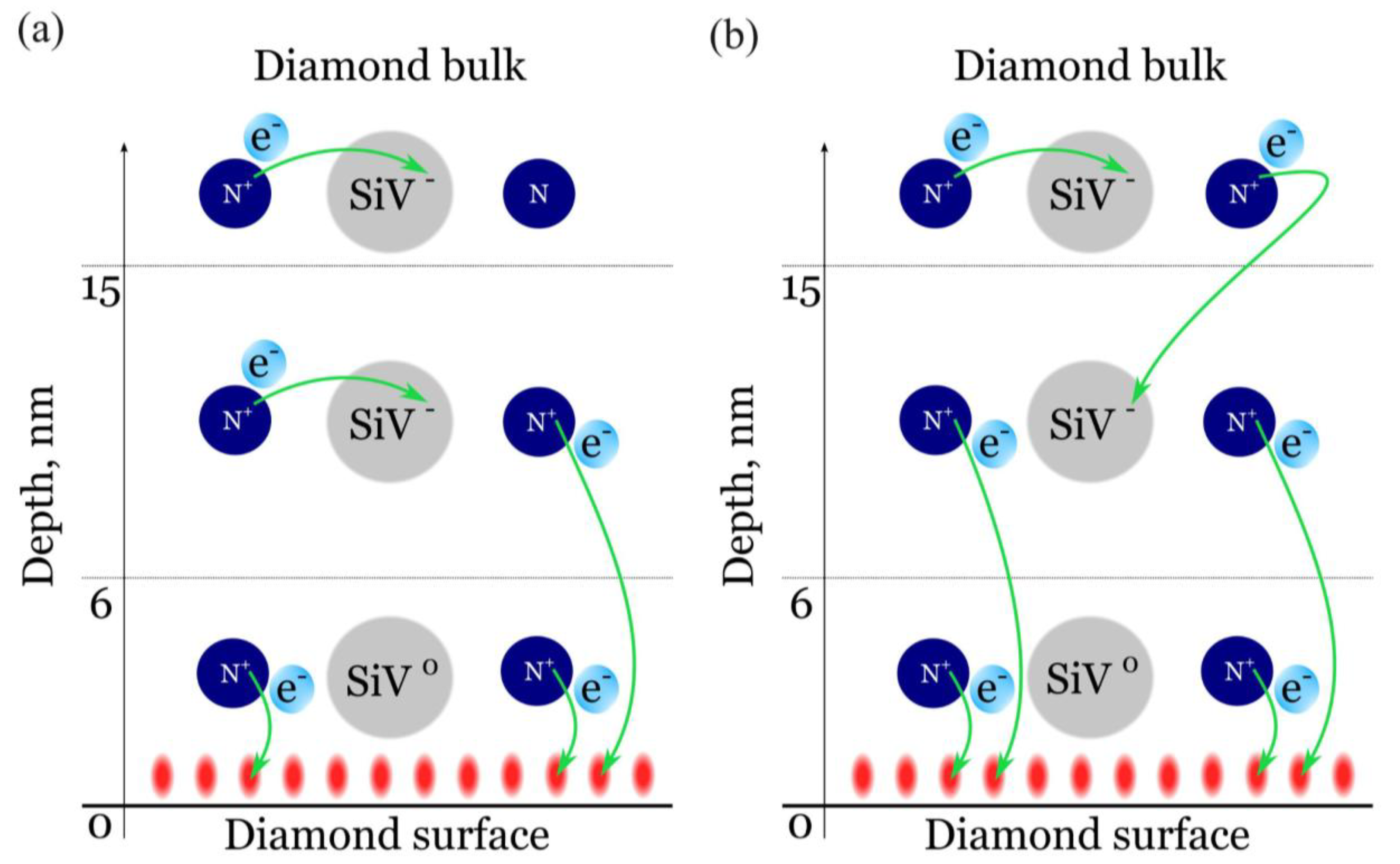
The main source of electrons required for the formation of negatively charged SiV centers (SiV⁻) is the donor-like substitutional nitrogen impurity presented in the diamond lattice [21,22,23,24,25]. Near the hydrogen-terminated diamond surface, two competing compensation channels for these nitrogen donors arise: (i) a thin (≈1 nm) layer of free holes, and (ii) neutral SiV0 centers. According to J. Ristein et al. [26], the holes recombine with electrons from nitrogen donors located up to ≈15 nm beneath the diamond surface. If this recombination channel is more efficient than donation of a nitrogen electron to the nearby SiV0, then SiV⁻ cannot form within this ≈15 nm region. Comparing the results of the present work with those of Ristein et al. [25], we find that the depth of the region where nitrogen donors are compensated by surface holes is approximately 2.5 times greater than the depth (≈6 nm) at which SiV centers remain neutral under hydrogen termination. This discrepancy can be rationalized by assuming that beyond 6 nm from the surface, the probability of nitrogen compensation by neighboring SiV0 is higher than by surface holes (Figure 6a). Alternatively, nitrogen located deeper than 15 nm from the surface can charge SiV0 located at depths within 6-15 nm from the surface (Figure 6b).
For the comparison, we refer to previously reported results on the influence of surface hydrogen on the charge states of SiV and NV centers in diamond nanostructures of different origins. In particular, Stehlik et al. [27] demonstrated that the intensity of SiV fluorescence decreases with decreasing thickness of polycrystalline CVD diamond films doped with silicon and terminated with hydrogen, and completely disappears at a thickness of less than 8 nm. Considering the 2-nm nucleation layer, the quenching of SiV emission occurs in the near-surface region with a thickness of about 6 nm. Thus, the estimates of the thickness of H-terminated layers suppressing SiV fluorescence in diamond films and nanoparticles are in good agreement with each other. In the work of Petráková et al. [28] ] the influence of the hydrogenated surface of milled HPHT diamond nanoparticles doped with nitrogen on the intensity of NV- fluorescence was studied. It was shown that NV- fluorescence completely quenched when the particle sizes were reduced to 20 nm, corresponding to an effective quenching layer thickness of 10 nm. These results indicate that hydrogen terminating a diamond surface exerts a stronger influence on the charge state of NV than SiV.
4. Conclusion
The effect of hydrogen-terminated surfaces on the SiV fluorescence intensity in HPHT NDs synthesized from hydrocarbons and doped with silicon was studied. SiV-fluorescent diamond nanoparticles with sizes ranging from 50 to 300 nm were analyzed before and after hydrogen removal from their surfaces. It was found that the influence of surface hydrogen termination on the SiV fluorescence becomes noticeable even for NDs with diameters around 300 nm, while a significant enhancement of fluorescence (>50%) upon hydrogen desorption occurs for particles smaller than ≈100 nm. From the measured dependence of SiV fluorescence intensities on particle sizes, we determined the effective thickness of the near-surface layer in which the charge neutralization of SiV⁻ centers takes place to be approximately 6 nm.
A new-generation of HPHT NDs synthesized from hydrocarbons are the promising nanomaterial for developing high-performance single photon sources and nanoscale optical sensors based on SiV- emission. These NDs exhibit high crystalline quality, and under optimized conditions of synthesis, they are essentially devoid of graphitic inclusions [14]. An intrinsic limitation for the practical application of such as-grown diamond nanoparticles is the presence of hydrogen on their surface, which induces suppression of SiV fluorescence near the surface. To overcome this drawback, a post-growth surface treatment is required to maximize the optical performance of SiV-based quantum emitters and sensors.
Author Contributions
Conceptualization: D.G.P., A.A.Z., A.M.R. and I.I.V.; methodology, D.G.P., A.A.Z., A.M.R.; HPHT synthesis R.H.B. and V.P.F.; Raman measurements, D.G.P., O.S.K.; PL measurements, A.A.Z., A.M.R.; writing—original draft preparation, D.G.P., A.A.Z. and I.I.V.; writing—review and editing, D.G.P., R.B., A.M.R. and I.I.V.; supervision, V.P.F. and I.I.V.; project administration, N.I.K. and I.I.V.; funding acquisition, N.I.K. All authors have read and agreed to the published version of the manuscript.
Funding
This study is supported by the Ministry of Science and Higher Education of the Russian Federation (agreement/grant 075-15- 2025-609).
Data Availability Statement
data are contained within the article.
Conflicts of Interest
the authors declare no conflict of interest.
References
- Alkahtani, M.; Lang, J.; Naydenov, B.; Jelezko, F.; Hemmer, P. Growth of High-Purity Low-Strain Fluorescent Nanodiamonds. ACS Photonics 2019, 6, 1266–1271. [Google Scholar] [CrossRef]
- Radtke, M.; Bernardi, E.; Slablab, A.; Nelz, R.; Neu, E. Nanoscale Sensing Based on Nitrogen Vacancy Centers in Single Crystal Diamond and Nanodiamonds: Achievements and Challenges. Nano Futur. 2019, 3, 042004. [Google Scholar] [CrossRef]
- Pasternak, D.G.; Romshin, A.M.; Zhivopistsev, A.A.; Bagramov, R.H.; Filonenko, V.P.; Vlasov, I.I. Bicolour Single Photon Source Based on HPHT Nanodiamond. Opt. Spectrosc. 2024, 132, 72. [Google Scholar] [CrossRef]
- Choi, S.; Leong, V.; Davydov, V.A.; Agafonov, V.N.; Cheong, M.W.O.; Kalashnikov, D.A.; Krivitsky, L.A. Varying Temperature and Silicon Content in Nanodiamond Growth: Effects on Silicon-Vacancy Centres. Sci. Rep. 2018, 8, 3792. [Google Scholar] [CrossRef] [PubMed]
- Fehler, K.G.; Ovvyan, A.P.; Antoniuk, L.; Lettner, N.; Gruhler, N.; Davydov, V.A.; Agafonov, V.N.; Pernice, W.H.P.; Kubanek, A. Purcell-Enhanced Emission from Individual SiV− Center in Nanodiamonds Coupled to a Si3 N4 -Based, Photonic Crystal Cavity. Nanophotonics 2020, 9, 3655–3662. [Google Scholar] [CrossRef]
- Nahra, M.; Alshamaa, D.; Deturche, R.; Davydov, V.; Kulikova, L.; Agafonov, V.; Couteau, C. Single Germanium Vacancy Centers in Nanodiamonds with Bulk-like Spectral Stability. AVS Quantum Sci. 2021, 3, 012001. [Google Scholar] [CrossRef]
- Romshin, A.M.; Pasternak, D.G.; Altakhov, A.S.; Bagramov, R.H.; Filonenko, V.P.; Vlasov, I.I. Temperature Characteristics of ”silicon-Vacancy“ Luminescent Centers in Diamond Particles Synthesized by Various Methods. Opt. Spectrosc. 2023, 131, 133. [Google Scholar] [CrossRef]
- Weil, T.; Liu, W.; Alam, M.N.A.; Liu, Y.; Agafonov, V.N.; Qi, H.; Koynov, K.; Davydov, V.A.; Uzbekov, R.; Kaiser, U.; et al. Silicon-Vacancy Nanodiamonds as High Performance Near-Infrared Emitters for Live-Cell Dual-Color Imaging and Thermometry. Nano Lett. 2022, 22, 2881–2888. [Google Scholar] [CrossRef]
- Wu, Y.; Alam, M.N.A.; Balasubramanian, P.; Ermakova, A.; Fischer, S.; Barth, H.; Wagner, M.; Raabe, M.; Jelezko, F.; Weil, T. Nanodiamond Theranostic for Light-Controlled Intracellular Heating and Nanoscale Temperature Sensing. Nano Lett. 2021, 21, 3780–3788. [Google Scholar] [CrossRef]
- Wu, Y.; Weil, T. Recent Developments of Nanodiamond Quantum Sensors for Biological Applications. Adv. Sci. 2022, 9, 2200059. [Google Scholar] [CrossRef]
- Pasternak, D.G.; Bagramov, R.H.; Romshin, A.M.; Zibrov, I.P.; Filonenko, V.P.; Vlasov, I.I. Controlled Formation of Silicon-Vacancy Centers in High-Pressure Nanodiamonds Produced from an “Adamantane + Detonation Nanodiamond” Mixture. Nanomaterials 2024, 14, 1843. [Google Scholar] [CrossRef]
- Alkahtani, M.H.; Alzahrani, Y.A.; Hazrathosseini, A.; Alessa, A.M.; Sow, M.; Alromaeh, A.; Alghihab, A.A.; Alghannam, F.S.; Jelezko, F.; Hemmer, P.R. Advanced Post-Treatment Strategy for Quantum-Grade Fluorescent Nanodiamonds. Front. Quantum Sci. Technol. 2025, 4, 1687810. [Google Scholar] [CrossRef]
- Kudryavtsev, O.S.; Bagramov, R.H.; Satanin, A.M.; Shiryaev, A.A.; Lebedev, O.I.; Romshin, A.M.; Pasternak, D.G.; Nikolaev, A.V.; Filonenko, V.P.; Vlasov, I.I. Fano-Type Effect in Hydrogen-Terminated Pure Nanodiamond. Nano Lett. 2022, 22, 2589–2594. [Google Scholar] [CrossRef] [PubMed]
- Kudryavtsev, O.S.; Bagramov, R.H.; Pasternak, D.G.; Satanin, A.M.; Lebedev, O.I.; Filonenko, V.P.; Vlasov, I.I. Raman Fingerprints of Ultrasmall Nanodiamonds Produced from Adamantane. Diam. Relat. Mater. 2023, 133, 109770. [Google Scholar] [CrossRef]
- Maier, F.; Riedel, M.; Mantel, B.; Ristein, J.; Ley, L. Origin of Surface Conductivity in Diamond. Phys. Rev. Lett. 2000, 85, 3472–3475. [Google Scholar] [CrossRef] [PubMed]
- Hauf, M.V.; Grotz, B.; Naydenov, B.; Dankerl, M.; Pezzagna, S.; Meijer, J.; Jelezko, F.; Wrachtrup, J.; Stutzmann, M.; Reinhard, F.; et al. Chemical Control of the Charge State of Nitrogen-Vacancy Centers in Diamond. Phys. Rev. B 2011, 83, 081304. [Google Scholar] [CrossRef]
- Khvostantsev, L.G.; Slesarev, V.N.; Brazhkin, V.V. Toroid Type High-Pressure Device: History and Prospects. High Press. Res. 2004, 24, 371–383. [Google Scholar] [CrossRef]
- Pasternak, D.G.; Romshin, A.M.; Bagramov, R.H.; Galimov, A.I.; Toropov, A.A.; Kalashnikov, D.A.; Leong, V.; Satanin, A.M.; Kudryavtsev, O.S.; Gritsienko, A.V.; et al. Donor–Acceptor Recombination Emission in Hydrogen-Terminated Nanodiamond. Adv. Quantum Technol. 2024, 2400263. [Google Scholar] [CrossRef]
- Cui, J.B.; Ristein, J.; Stammler, M.; Janischowsky, K.; Kleber, G.; Ley, L. Hydrogen Termination and Electron Emission from CVD Diamond Surfaces: A Combined Secondary Electron Emission, Photoelectron Emission Microscopy, Photoelectron Yield, and Field Emission Study. Diam. Relat. Mater. 2000, 9, 1143–1147. [Google Scholar] [CrossRef]
- Schindelin, J.; Arganda-Carreras, I.; Frise, E.; Kaynig, V.; Longair, M.; Pietzsch, T.; Preibisch, S.; Rueden, C.; Saalfeld, S.; Schmid, B.; et al. Fiji: An Open-Source Platform for Biological-Image Analysis. Nat. Methods 2012, 9, 676–682. [Google Scholar] [CrossRef]
- Green, B.L.; Collins, A.T.; Breeding, C.M. Diamond Spectroscopy, Defect Centers, Color, and Treatments. Rev. Mineral. Geochem. 2022, 88, 637–688. [Google Scholar] [CrossRef]
- Garcia-Arellano, G.; López-Morales, G.I.; Manson, N.B.; Flick, J.; Wood, A.A.; Meriles, C.A. Photo-Induced Charge State Dynamics of the Neutral and Negatively Charged Silicon Vacancy Centers in Room-Temperature Diamond. Adv. Sci. 2024, 11, 2308814. [Google Scholar] [CrossRef]
- Dhomkar, S.; Zangara, P.R.; Henshaw, J.; Meriles, C.A. On-Demand Generation of Neutral and Negatively Charged Silicon-Vacancy Centers in Diamond. Phys. Rev. Lett. 2018, 120, 117401. [Google Scholar] [CrossRef] [PubMed]
- Pederson, C.; Yama, N.S.; Beale, L.; Markham, M.; Turiansky, M.E.; Fu, K.-M.C. Rapid, in Situ Neutralization of Nitrogen- and Silicon-Vacancy Centers in Diamond Using Above-Band Gap Optical Excitation. Nano Lett. 2025, 25, 673–680. [Google Scholar] [CrossRef] [PubMed]
- Breeze, B.G.; Meara, C.J.; Wu, X.X.; Michaels, C.P.; Gupta, R.; Diggle, P.L.; Dale, M.W.; Cann, B.L.; Ardon, T.; D’Haenens-Johansson, U.F.S.; et al. Doubly Charged Silicon Vacancy Center, Si-N Complexes, and Photochromism in N and Si Codoped Diamond. Phys. Rev. B 2020, 101, 184115. [Google Scholar] [CrossRef]
- Ristein, J.; Riedel, M.; Stammler, M.; Mantel, B.F.; Ley, L. Surface Conductivity of Nitrogen-Doped Diamond. Diam. Relat. Mater. 2002, 11, 359–364. [Google Scholar] [CrossRef]
- Stehlik, S.; Varga, M.; Stenclova, P.; Ondic, L.; Ledinsky, M.; Pangrac, J.; Vanek, O.; Lipov, J.; Kromka, A.; Rezek, B. Ultrathin Nanocrystalline Diamond Films with Silicon Vacancy Color Centers via Seeding by 2 Nm Detonation Nanodiamonds. ACS Appl. Mater. Interfaces 2017, 9, 38842–38853. [Google Scholar] [CrossRef]
- Petráková, V.; Taylor, A.; Kratochvílová, I.; Fendrych, F.; Vacík, J.; Kučka, J.; Štursa, J.; Cígler, P.; Ledvina, M.; Fišerová, A.; et al. Luminescence of Nanodiamond Driven by Atomic Functionalization: Towards Novel Detection Principles. Adv. Funct. Mater. 2012, 22, 812–819. [Google Scholar] [CrossRef]
Figure 1.
(a) Optical image of diamond nanoparticles distributed over a silicon substrate. Lilac dotted circles indicate representative ND spots selected for PL analysis. (b) A typical PL spectrum from one of the ND spots recorded under 660-nm laser excitation shows SiV line at 738,5 nm and the line of second-order Raman scattering from a Si substrate.
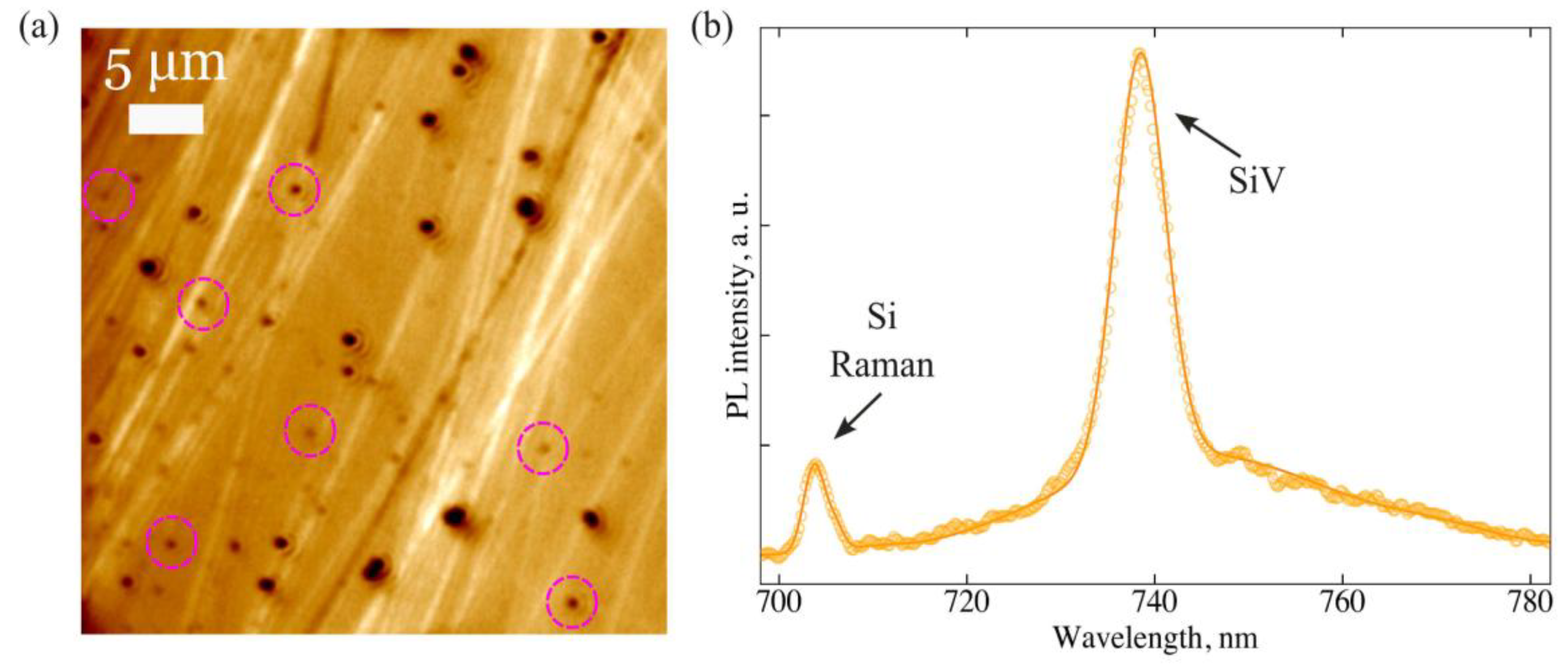
Figure 2.
(a) The SEM image of a representative cluster of “reference” NDs (30–50 nm grain size) selected for hydrogen removal by an electron beam. (b) Raman spectra of the same ND cluster recorded before (blue) and after (orange) electron-beam treatment (laser radiation wavelength is 532 nm, and laser power ≈100 μW).
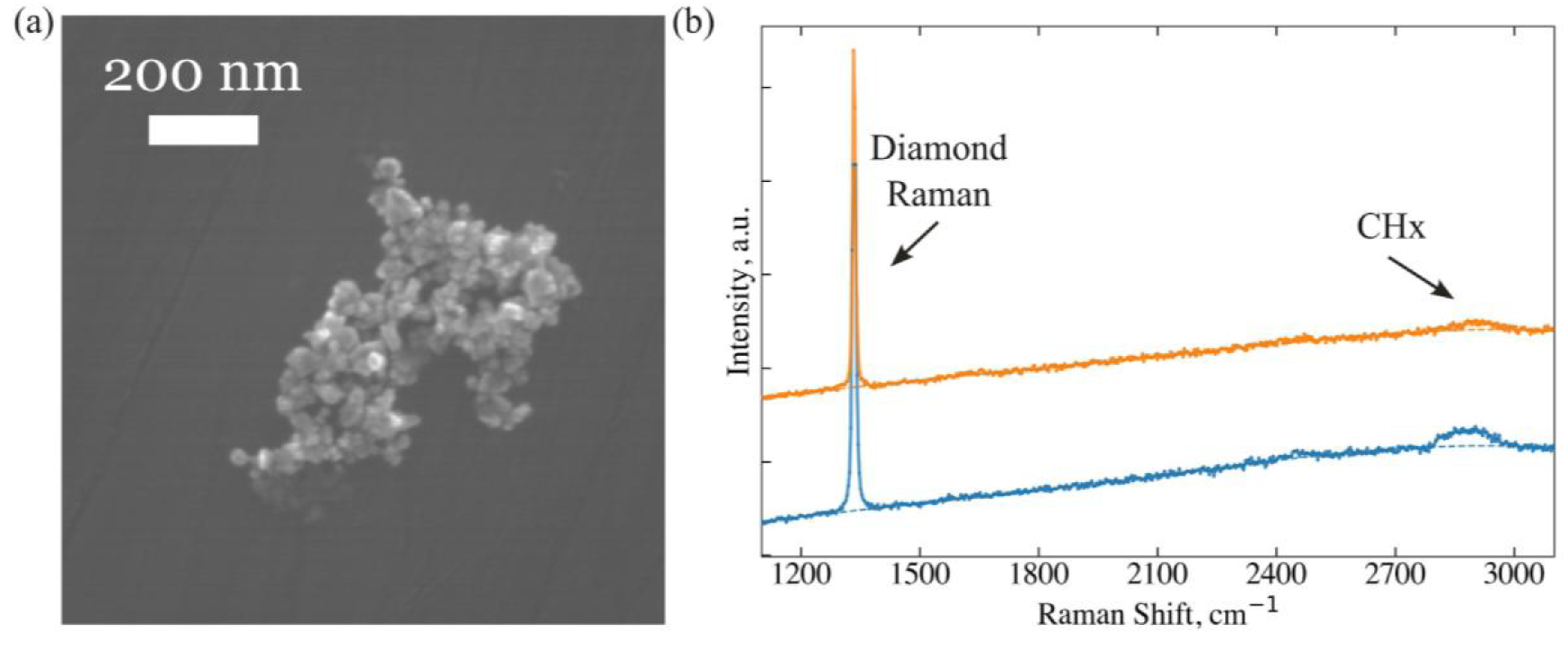
Figure 3.
The characteristic SEM images of SiV-fluorescent NDs. Their estimated sizes are 70 nm (a) and 270 nm (b).
Figure 3.
The characteristic SEM images of SiV-fluorescent NDs. Their estimated sizes are 70 nm (a) and 270 nm (b).
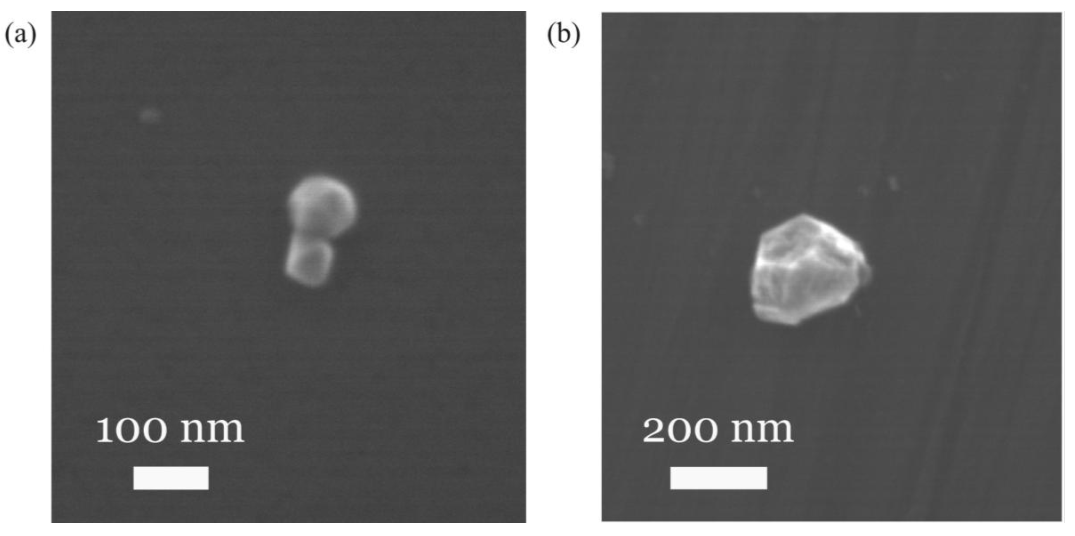
Figure 4.
Comparative curves of SiV fluorescence saturation measured for different NDs before (blue) and after (orange) hydrogen desorption. Data for NDs with the diameters of 70 nm (a) and 250 nm (b). The plots show the fluorescence count rate I of SiV PL as a function of laser excitation power P (λexс=660 nm). The circles are the background-corrected experimental data, and the solid lines fit to the saturation function
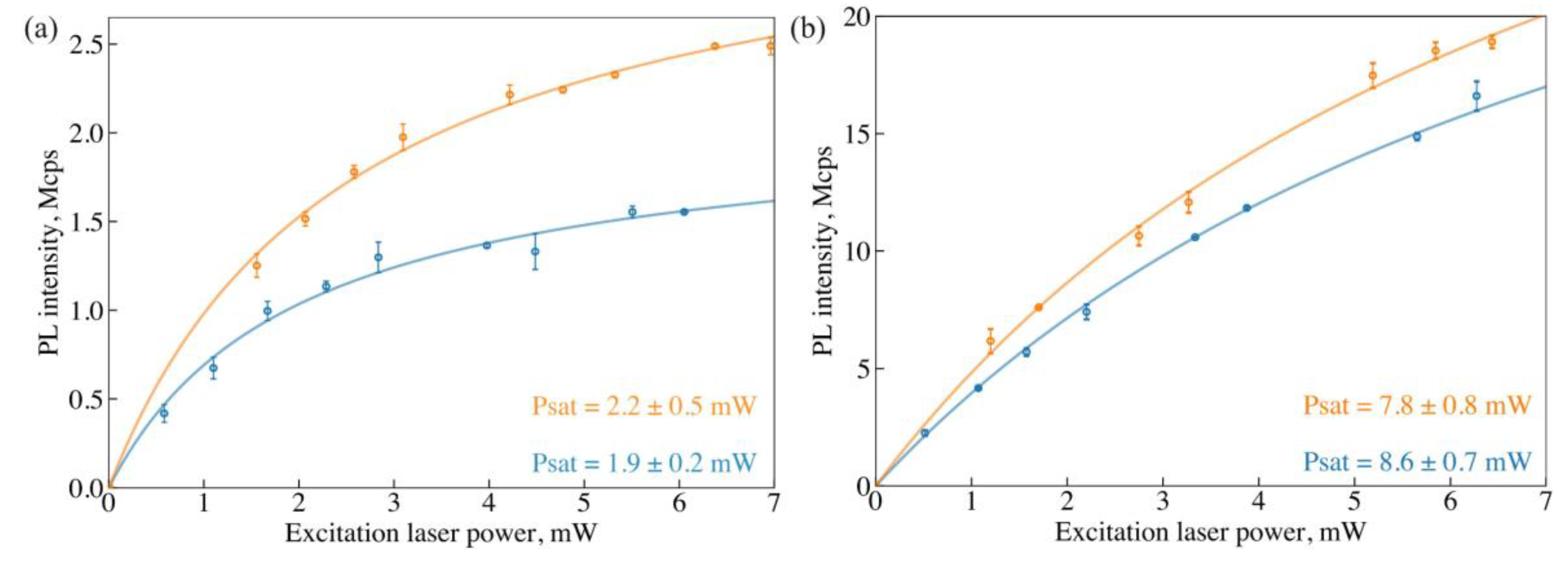
Figure 5.
The dependence of the relative increase in SiV fluorescence intensity
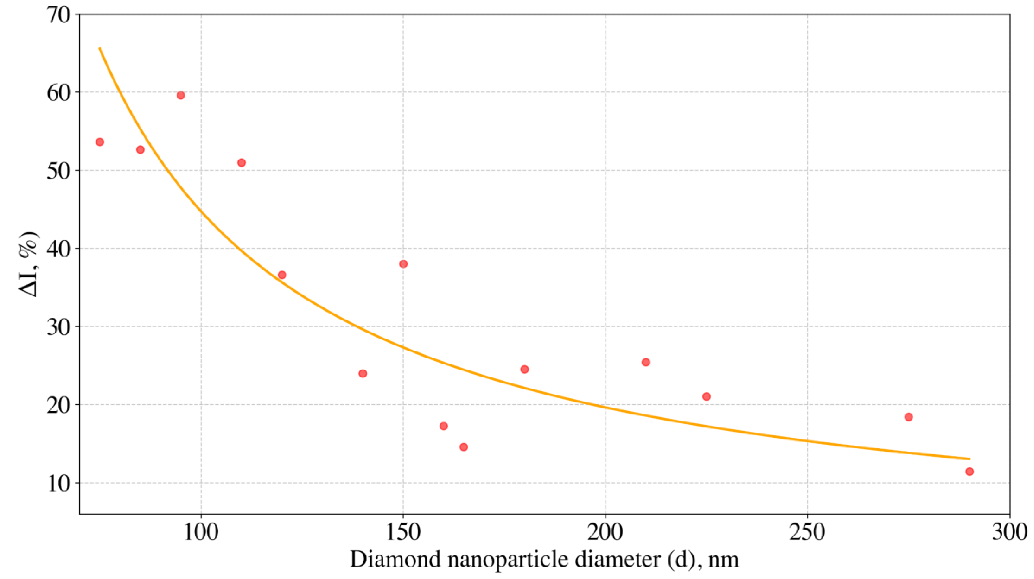
Figure 6.
Schematic illustration of possible interactions of donor nitrogen with SiV and near-surface holes next to H-terminated diamond surface. Within 6 nm from the surface N donates electrons predominantly to the surface holes, and SiV0 remains uncharged. At depths within 6-15 nm SiV0 can transfer to SiV- in two ways: (a) N donates an electron to neighboring SiV0 with higher probability than to surface holes; (b) SiV0 is negatively charged by N located more than 15 nm from the surface.
Disclaimer/Publisher’s Note: The statements, opinions and data contained in all publications are solely those of the individual author(s) and contributor(s) and not of MDPI and/or the editor(s). MDPI and/or the editor(s) disclaim responsibility for any injury to people or property resulting from any ideas, methods, instructions or products referred to in the content. |
© 2025 by the authors. Licensee MDPI, Basel, Switzerland. This article is an open access article distributed under the terms and conditions of the Creative Commons Attribution (CC BY) license (http://creativecommons.org/licenses/by/4.0/).
Copyright: This open access article is published under a Creative Commons CC BY 4.0 license, which permit the free download, distribution, and reuse, provided that the author and preprint are cited in any reuse.


