Submitted:
07 November 2025
Posted:
07 November 2025
You are already at the latest version
Abstract
Mesoporous silica and its derivatives might enable applications ranging from biomedicine
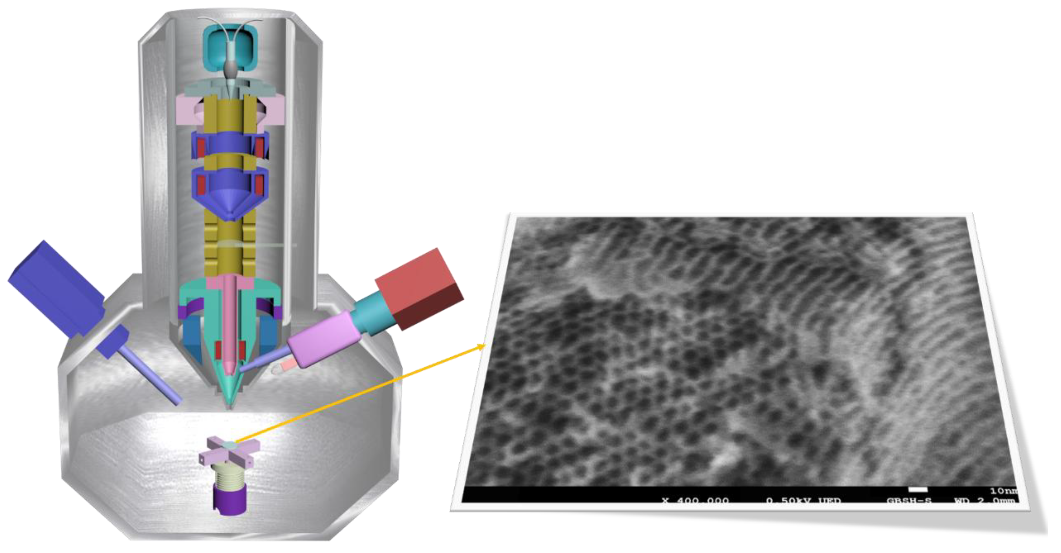
to petrochemical processing. Transmission electron microscopy (TEM), X-ray diffraction (XRD) and N2 adsorption-desorption measurements are usually used to characterize the ordered porous system. However, all these methods are short of conveying full surface information. In this work, low voltage scanning electron microscope (LVSEM) with beam deceleration technology was employed to image detailed surface pore structures of a ~2 nm pores diameters silica (MCM-41), SBA-15, KIT-6 and mesoporous silica nanospheres (MSNSs). The prospect for the development direction on ultra-high resolution Scanning Electron Microscopy (SEM) application was discussed in characterization of ordered porous materials. We demonstrate that complete dimension range of mesoscopic surface structure (2-50 nm) could be resolved by current low voltage SEM technology.
Keywords:
scanning electron microscopy
; mesoporous silica
; surface details
Mesoporous silica and its derivatives might enable applications ranging from biomedicine to petrochemical processing. Transmission electron microscopy (TEM), X-ray diffraction (XRD) and N2 adsorption-desorption measurements are usually used to characterize the ordered porous system. However, all these methods are short of conveying full surface information. In this work, low voltage scanning electron microscope (LVSEM) with beam deceleration technology was employed to image detailed surface pore structures of a ~2 nm pores diameters silica (MCM-41), SBA-15, KIT-6 and mesoporous silica nanospheres (MSNSs). The prospect for the development direction on ultra-high resolution Scanning Electron Microscopy (SEM) application was discussed in characterization of ordered porous materials. We demonstrate that complete dimension range of mesoscopic surface structure (2-50 nm) could be resolved by current low voltage SEM technology.
The invention of Mobil Composition of Matter No. 41 (MCM-41) [1] triggered an explosion of research into mesoporous materials, which have been intensively studied for applications as diverse as catalysis [2,3], molecular adsorption [4,5], drug delivery [6,7], molecular separations using membranes [8,9], energy [10] and templates for synthesis of advanced nanomaterials [11,12]. Transmission electron microscopy (TEM) was broadly used to characterize these ordered porous systems [13,14,15]. Different from TEM and Scanning Transmission Electron Microscopy (STEM) with weak surface sensitivity, Scanning Electron Microscopy (SEM) could reveal detailed information on the more microscopic surface structure [16]. However, the practical spatial resolution of SEM was still limited by inclusion of delocalized secondary electrons (SE) components [17], charge effect and instrument itself [18]. Low voltage coupled with in-lens detector could control the signals were dominated by SE1 component that are emitted from a small escape depth under the specimen surface after direct excitation by the incident electron beam and ease the charging on non-conducting materials. Terasaki et al. [19] first reported Low Voltage Scanning Electron Microscopy (LVSEM) direct observation of 3D mesoporous structure of Santa Barbara No. 15 (SBA-15) with ~7.5 nm pore diameters and ~2.5 nm thickness of pore wall at 2 kV. Bao et al. [20] imaged a series fined controlled pore length of SBA-15 materials by using a classic cold field emission SEM instrument (Hitachi S4800) at 1.5 kV. However, the imaging performance of LVSEM like resolution and contrast could be improved by using beam deceleration technology [16], which may further reduce interaction volume of incident electrons and specimens.
Another way to improve the spatial resolution of SEM was observing the transmission samples at relatively high voltage like 10 kV, 30 kV or even 200 kV [21,22]. In this method, smaller lateral spot size could be controlled easily and most incident electrons directly pass through the sample which might reduce lateral delocalized secondary electrons (SE2 and SE3) components, and then the percentage of SE1 component could be increased. Tüysüz et al. [21] first resolved the high-resolution SEM images of ~2 nm pore size MCM-41 at 10 kV without any beam deceleration. However, the charge and beam damage caused by high landing energy could not be overlooked.
Herein, we report that we can directly image the distinct surface structures of a 7 nm pore diameter SBA-15 and even a ~2.0 nm pore diameter MCM-41 mesoporous silica by using negative specimens stage bias beam deceleration technology. 500 eV landing energy LVSEM and a 200 kV SEM technology were used to direct image of a ~2.0 nm pore diameter silica. High quality SEM images could be provided by these means. Imaging capabilities mechanisms for the results at different conditions are discussed by comparing with each other using Monte Carlo simulation.
All these results will allow a better understanding of the accessibility of the porous systems of ordered mesoporous materials. The two methods, especially low voltage low probe current SEM with beam deceleration technology, could be extended to other mesoporous materials like beam sensitive mesoporous MOF, COF [23], mesoporous carbon materials or under 5 nm particles materials system. These also demonstrate that complete dimension range of mesoscopic surface structure (2-50 nm) could be resolved by current LVSEM technology.
1. Result and Discussion
According to literature procedures, ~7 nm pore diameters SBA-15 [19], ~6 nm pore diameters KIT-6 [21], ~3 nm pore diameters mesoporous silica nanospheres (MSNSs) [24] and ~2 nm pore diameters MCM-41 mesoporous silica [21] were prepared. All samples were characterized with small angle X-Ray Diffraction (XRD, Figure S1a), N2-sorption (Figure S1b, c) and High-Resolution Transmission Electron Microscopy (HRTEM). Properties obtained from small angle XRD and N2 adsorption–desorption measurement are summarized in Table 1. Figure 1 shows HRTEM images of as-prepared SBA-15, KIT-6, MCM-41 and MSNSs. TEM images (Figure 1a~c) and corresponding Fast Fourier Transform (FFT) patterns (Figure 1e~g) revealed hexagonally ordered mesoporous structure of SBA-15, KIT-6 and MCM-41. The images analysis gave the SBA-15 pore diameters ~7.09 nm with wall thickness ~3.12 nm, KIT-6 pore diameters ~6.87 nm and wall thickness ~2.21nm, MCM-41 pore diameters ~2.00 nm and wall thickness ~1.73 nm. Figure 1d and 1h suggest the as-prepared MSNSs pore system were not spatial translation symmetry.
Before LVSEM characterization, the dependence of surface details on accelerating voltage was explored by Monte Carlo simulations and a simple control experiment were conducted (Figure 2). Figure 2a shows simulations of 2000 electrons with 15 keV kinetic energy are vertically incident to carbon (spot size = 1 nm). The interaction depth is about 2 μm, so the SEM image of TEM copper grids can only see the copper grids without covered carbon film (Figure 2d). But when the accelerating voltage decreased to 2.5 kV, the interaction depth reduced to about 85 nm (Figure 2b), translucent carbon film can be resolved on the copper grids (Figure 2e). Further decrease the accelerating voltage to 500 V, the interaction depth reduced to about 6 nm (Figure 2c), opaque carbon film was found covered the copper grids (Figure 2f). These results suggest that too high accelerating voltage can result in deeper interaction depth in samples which might lead to missing the surface details of SEM images.
However, low voltage high resolution SEM technology could be divided into directly low voltage (Figure 3a), stage bias beam deceleration (Figure 3b) and in-column beam deceleration (Figure 3c). Firstly, direct decrease the accelerating voltage to 500 V~1 kV, both the in-lens detector and Everhart-Thornley (E-T) detector could collect SE images of samples by adding positive bias on the surface of these detectors. We succeed in obtaining surface details of SBA-15 (Figure S2) with E-T detector at 1 kV, which are very rare in former researches. However, the image quality is unsatisfactory because the E-T detector images are enriched with SE2 and SE3 signals [17]. The in-lens detector images possess more surface details, even at 500 V without any beam deceleration, we could image the parallel channels on the surface of mesoporous SBA-15 (Figure S3), the images quality is comparable to the literature [20,25,26]. Beam deceleration with negative stage bias could lower the interaction volume of electrons in samples, release the charge effect, accelerate the low energy SE1 to in-lens detectors and change the low angle backscattered electrons (BSE) direction of motion to higher angle (Figure 3b). Hence, we obtained decent SBA-15 images by a BSE detector with the landing energy only 500 eV (Figure S4a). Even so, the BSE signals is still not an ultra-high resolution method for smaller details compare to SE1. Considering the low energy SE1 are accelerated by the retarding field, concentric annular in-lens detector (Figure 3b, in-lens detector 1) might receive more electrons than side position in-lens detector (Figure 3b, in-lens detector 2). So, the S/N rate of Figure S4b side position in-lens detector image is not very well. It is also efficient to improve the concentric annular in-lens detector images by increasing the stage bias from 2 kV to 5 kV [30]. Compared to Figure S5b, the S/N is improved and even the inter-channel micropores and plugs within channels can be observed in Figure S5a. Nevertheless, the weaknesses of this technology are the sharp surface samples might result in point discharge and small depth of field due to small interaction volume, which might cause difficulties to image bulk KIT-6 (Figure S6). One another low voltage technology is in-column beam deceleration. If the surface of samples were very close to the bottom of final lens (working distance, under 1 mm), the excited SE1 can easily sucked into the column and accelerated by the in-column retarding field (Figure 3c). In this case, concentric annular in-lens detectors can ensure well S/N rate even at a very low probe current conditions. The weakness of this technology is very short working distance need the smooth surface of samples.
According to the above, concentric annular in-lens detector coupled with high stage bias or in-column beam deceleration might provide ultra-high resolution at very low probe current and low landing energy conditions. In this work, both the two technologies were employed to direct image SBA-15, KIT-6, MSNSs and MCM-41.
Figure 4 displays LVSEM images of the as-prepared SBA-15 and KIT-6. Figure S7 shows low magnification images of SBA-15, the morphology is bend hexagonal prisms. One can clearly see that the ordered mesoporous channels are fully exposed on the side of hexagonal prisms as well as the inter-channel micropores and plugs within channels (Figure 4a), the cross section of hexagonal prisms are hexagonally arranged circular holes structure with ups and downs on the surface (Figure 4b). Fine surface structural details and high S/N rate LVSEM images of SBA-15 were obtained. Image analysis gave the pore size and wall thickness of SBA-15 are about 6.7 and 3.4 nm, respectively.
KIT-6 is cubic structure with Iad symmetry and two types of channel are connected with each other through smaller pores [21]. Large particle topography and highly connected pore system result in severe charge effect and high beam sensitivity. Even at 1 keV low landing energy of incident electron beam, there are still existing obvious beam damage (Figure S8a). Although the decrease the probe current to 1.6 pA (Figure S8b) or select a new designed cold field emission SEM (Figure S8c), the pore system images are different to the reported results [21]. Therefore, 500 eV land energy with tiny probe current were used to collect the LVSEM images of KIT-6 (Figure 4c,4d, Figure S9). A whole bulk of KIT-6 surface fine pore system was obtained (Figure S9a). There are obvious steps (Figure S9a), kinks, vacancies and ledges (Figure 4c, 4d, Figure S9b) on the surface of KIT-6, which might be benefit from the well focus depth of none stage bias in-column beam deceleration technology. We can clear see the various pores were connected each other and short-range ordered, which might because the surface is corrugated and is not terminated along well-defined crystal planes. If the surface was polished with Ar ion, long-range ordered pore structure could be observed [31]. Pore size and wall thickness of KIT-6 are about 6.3 nm and 3.8 nm, which is agree with other methods.
Although the high resolution LVSEM has made tremendous progress, under 3 nm porous materials LVSEM image reports were very rare [21]. Figure 5a, 5b, Figure S10 show the morphology of MSNSs are nanospheres with unordered craters on the surface. The absence of parallel channels suggests that the mesoporous might be 3D-dendritic. Pore size of MSNSs is about 2.8 nm. Figure 5c and 5d show ultra-high magnification LVSEM images of MCM-41 with 500 eV landing energy. There is some amorphous silica can be seen on the surface of MCM-41 in Figure 5c, but regular hexagonal array of uniform channels can also be found in Figure 5d. The image analysis gave the pore size only range from 1.8 nm-2.1 nm and the wall thickness is about 1.7 nm. Figure S11 shows a 1 keV land energy LVSEM image of the MCM-41, too high landing energy of incident electron beam result in poor practical spatial resolution. Anyway, these results not only give the high-quality surface details of several mesoporous silica, but also mark that current under 500 eV LVSEM can also directly resolve about 1.8 nm ordered details on the surface.
Interestingly, 200 kV high voltage SEM can also directly image the ~2 nm pore size MCM-41. Figure 6a shows a 200kV SEM image of MCM-41, while Figure 6b is a high-angle annular dark field scanning transmission electron microscope (HAADF-STEM) simultaneous image. The contrast and the S/N rate are also higher than the LVSEM images. The regular hexagonal array of uniform channels is more obvious, this might because the detail loss of amorphous silica on the surface. To figure out the reasons, Monte Carlo simulations of 2000 electrons were conducted with 200 keV kinetic energy are vertically incident to a 100 nm SiO2 membrane supported by carbon (Figure 6c, Figure 6d is magnified of Figure 6c). From Figure 6d, almost all electrons breakdown the SiO2 layer and almost no scattering has appeared in SiO2 layer. If the substrate is practical ~20 nm carbon membrane supported, the lateral resolution of SEM and STEM are very close to the spot size (~1 nm) of incident electron beam. However, in this method, the sample must be prepared as a TEM sample, and large bulk may also result in charging effect, which might lead to image shift or loss of surface details.
2. Conclusions
In conclusion, we reviewed the advance of ultra-high resolution SEM technology, benefits and drawbacks of every technologies and the application on imaging of mesoporous silica. We have directly imaged ~7 nm pore size SBA-15, ~6 nm pore size KIT-6, ~3 nm pore size MSNSs and even ~2 nm pore size MCM-41 by under 500 V LVSEM with beam deceleration technology. It has been demonstrated that the under 500 V LVSEM technique can directly resolve about 1.8 nm ordered details on the surface. Unprecedented highest quality 3D topography and surface pore system images of these four kinds of mesoporous silica were provided. These results will allow a better understanding of the pore systems structure and applications of ordered mesoporous materials. Two methods were discussed and demonstrated be efficient to obtained high resolution SEM images of mesoporous silica, those are LVSEM and 200 kV high voltage SEM.
Supplementary Materials
The following supporting information can be downloaded at the website of this paper posted on Preprints.org.
Acknowledgments
This work was supported by the Natural Science Foundation of Jiangsu Province, China (Grant No. BK20201246) National Natural Science Foundation of China (Grant No. 12 274 202).
Conflicts of interest
There are no conflicts of interest to declare.
TOC:
References
- Kresge, C.; Leonowicz, M.; Roth, W.; Vartuli, J.; Beck, J. Ordered mesoporous molecular sieves synthesized by a liquid crystal template mechanism. Nature 1992, 359, 710–712. [Google Scholar] [CrossRef]
- Orazov, M.; Davis, M. ; Catalysis by framework zinc in silica-based molecular sieves. Chem. Sci. 2016, 7, 2264–2274. [Google Scholar] [CrossRef]
- Sun, B.; Zhou, W.; Li, H.; Ren, L.; Qiao, P.; Li, W.; Fu, H. Synthesis of Particulate Hierarchical Tandem Heterojunctions toward Optimized Photocatalytic Hydrogen Production. Adv. Mater. 2018, 30, 1804282−1804290. [Google Scholar] [CrossRef]
- Potter, M.; Pang, S.; Jones, C. Adsorption Micro-calorimetry of CO2 in Confined Amino polymers. Langmuir 2017, 33, 117–124. [Google Scholar] [CrossRef]
- Gunathilake, C.; Jaroniec, M. ; Mesoporous calcium oxide-silica and magnesium oxide-silica composites for CO2 capture at ambient and elevated temperatures. J. Mat. Chem. A 2016, 4, 10914–10924. [Google Scholar] [CrossRef]
- Fang, Y.; Zheng, G.; Yang, J.; Tang, H.; Zhang, Y.; Kong, B.; Lv, Y.; Xu, C.; Asiri, A.; Zi, J.; Zhang, F.; Zhao, D. Dual-Pore Mesoporous Carbon@Silica Composite Core−Shell Nanospheres for Multidrug Delivery. Angew. Chem. Int. Ed. 2014, 126, 5470−5474. [Google Scholar] [CrossRef]
- Lin, F.; Zink, J. Probing the Local Nanoscale Heating Mechanism of a Magnetic Core in Mesoporous Silica Drug-Delivery Nanoparticles Using Fluorescence Depolarization. J. Am. Chem. Soc. 2020, 142, 5212–5220. [Google Scholar] [CrossRef] [PubMed]
- Liu, Y.; Shen, D.; Chen, G.; Elzatahry, A.; Pal, M.; Zhu, H.; Wu, L.; Lin, J.; Al-Dahyan, D.; Li, W.; Zhao, D. Mesoporous Silica Thin Membranes with Large Vertical Mesochannels for Nanosize-Based Separation. Adv. Mater. 2017, 29, 1702274. [Google Scholar] [CrossRef] [PubMed]
- Yan, W.; Shi, M.; Wang, Z.; Zhou, Y.; Liu, L.; Zhao, S.; Ji, Y.; Wang, J.; Gao, C. Amino-modified hollow mesoporous silica nanospheres-incorporated reverse osmosis membrane with high performance. J. Membr. Sci. 2019, 581, 168–177. [Google Scholar] [CrossRef]
- Li, W.; Liu, J.; Zhao, D. Mesoporous Materials for Energy Conversion and Storage Devices. Nat. Rev. Mater. 2016, 1, 16023−16040. [Google Scholar] [CrossRef]
- Kani, K.; Malgras, V.; Jiang, B.; Hossain, M.; Alshehri, S.; Ahamad, T.; Salunkhe, R.; Huang, Z.; Yamauchi, Y. Periodically Arranged Arrays of Dendritic Pt Nanospheres Using Cage-Type Mesoporous Silica as a Hard Template. Chem. Asian J. 2018, 13, 106–110. [Google Scholar] [CrossRef] [PubMed]
- Dirin, D.; Protesescu, L.; Trummer, D.; Kochetygov, I.; Yakunin, S.; Krumeich, F.; Stadie, N.; Kovalenko, M. Harnessing defect-tolerance at the nanoscale: highly luminescent lead halide perovskite nanocrystals in mesoporous silica matrixes. Nano Lett. 2016, 16, 5866–5874. [Google Scholar] [CrossRef]
- Carlsson, A.; Kaneda, M.; Sakamoto, Y.; Terasaki, O.; Ryoo, R.; Joo, S. The structure of MCM–48 determined by electron crystallography. J. Electron Microsc. 1999, 48, 795–798. [Google Scholar] [CrossRef]
- Sakamoto, Y.; Kaneda, M.; Terasaki, O.; Zhao, D.; Kim, J.; Stucky, G.; Shin, H.; Ryoo, R. Direct imaging of the pores and cages of three-dimensional mesoporous materials. Nature 2000, 408, 449–453. [Google Scholar] [CrossRef]
- Kaneda, M.; Tsubakiyama, T.; Carlsson, A.; Sakamoto, Y.; Ohsuna, T.; Terasaki, O.; Joo, S.; Ryoo, R. Structural study of mesoporous MCM-48 and carbon networks synthesized in the spaces of MCM-48 by electron crystallography. J. Phys. Chem. B 2002, 106, 1256–1266. [Google Scholar] [CrossRef]
- Asahina, S.; Uno, S.; Suga, M.; Stevens, S.; Klingstedt, M.; Okano, Y.; Kudo, M.; Schüth, F.; Anderson, M.; Adschiri, T.; Terasaki, O. A new HRSEM approach to observe fine structures of novel nanostructured materials. Microporous and Mesoporous Materials 2011, 146, 11–17. [Google Scholar] [CrossRef]
- Zhang, X.; Cen, X.; Ravichandran, R.; Hughes, L.; Benthem, K. Simultaneous scanning electron microscope imaging of topographical and chemical contrast using in-lens, in-column, and everhart-thornley detector systems. Microscopy and Microanalysis 2016, 22, 565–575. [Google Scholar] [CrossRef] [PubMed]
- Joy, D. Control of charging in low-voltage SEM. Scanning, 1989, 11, 1–4. [Google Scholar] [CrossRef]
- Che, S.; Lund, K.; Tatsumi, T.; Iijima, S.; Joo, S.; Ryoo, R.; Terasaki, O. Direct observation of 3D mesoporous structure by scanning electron microscopy (SEM): SBA-15 silica and CMK-5 carbon. Angew. Chem. Int. Ed. 2003, 42, 2182–2185. [Google Scholar] [CrossRef]
- Zhang, H.; Sun, J.; Ma, D.; Weinberg, G.; Su, D.; Bao, X. Engineered Complex Emulsion System: Toward Modulating the Pore Length and Morphological Architecture of Mesoporous Silicas. J. Phys. Chem. B 2006, 110, 25908–25915. [Google Scholar] [CrossRef]
- Tüysüz, H.; Lehmann, C.; Bongard, H.; Tesche, B.; Schmidt, R.; Schüth, F. Direct Imaging of Surface Topology and Pore System of Ordered Mesoporous Silica (MCM-41, SBA-15, and KIT-6) and Nanocast Metal Oxides by High Resolution Scanning Electron Microscopy. J. Am. Chem. Soc. 2008, 130, 11510–11517. [Google Scholar] [CrossRef]
- Inada, H.; Su, D.; Egerton, R.; Konno, M.; Wu, L.; Ciston, J.; Wall, J.; Zhu, Y. Atomic imaging using secondary electrons in a scanning transmission electron microscope: Experimental observations and possible mechanisms. Ultramicroscopy 2011, 111, 865–876. [Google Scholar] [CrossRef]
- Deng, H.; Grunder, S.; Cordova, K.; Valente, C.; Furukawa, H.; Hmadeh, M.; Gándara, F.; Whalley, A.; Liu, Z.; Asahina, S.; Kazumori, H.; Keeffe, M.; Terasaki, O.; Stoddart, J.; Yaghi, O. Large-Pore Apertures in a Series of Metal-Organic Frameworks. Science 2012, 336, 1018–1023. [Google Scholar] [CrossRef]
- Shen, D.; Yang, J.; Li, X.; Zhou, L.; Zhang, R.; Li, W.; Chen, L.; Wang, R.; Zhang, F.; Zhao, D. Biphase Stratification Approach to Three-Dimensional Dendritic Biodegradable Mesoporous Silica Nanospheres. Nano Lett. 2014, 14, 923–932. [Google Scholar] [CrossRef]
- Sayari, A.; Han, B.; Yang, Y. Simple Synthesis Route to Monodispersed SBA-15 Silica Rods. J. Am. Chem. Soc. 2004, 126, 14348–14349. [Google Scholar] [CrossRef]
- Zhang, H.; Sun, J.; Ma, D.; Bao, X.; Klein-Hoffmann, A.; Weinberg, G.; Su, D.; Schlögl, R. Unusual Mesoporous SBA-15 with Parallel Channels Running along the Short Axis. J. Am. Chem. Soc. 2004, 126, 7440–7441. [Google Scholar] [CrossRef]
- Endo, A.; Yamada, M.; Kataoka, S.; Sano, T.; Inagi, Y.; Miyaki, A. Direct observation of surface structure of mesoporous silica with low acceleration voltage FE-SEM. Colloids and Surfaces A: Physicochem. Eng. Aspects. 2010, 357, 11–16. [Google Scholar] [CrossRef]
- Kataoka, S.; Takeuchi, Y.; Kawai, A.; Yamada, M.; Kamimura, Y.; Endo, A. Controlled Formation of Silica Structures Using Siloxane/Block Copolymer Complexes Prepared in Various Solvent Mixtures. Langmuir, 2013, 29, 13562–13567. [Google Scholar] [CrossRef] [PubMed]
- Zhang, Z.; Wei, X.; Yao, Y.; Chen, Z.; Zhang, A.; Li, W.; Wu, W.; Wu, Z.; Chen, X. Zhao, D. Conformal Coating of Co/N-Doped Carbon Layers into Mesoporous Silica for Highly Efficient Catalytic Dehydrogenation-Hydrogenation Tandem Reactions. Small, 2017, 13, 1702243. [Google Scholar] [CrossRef] [PubMed]
- Suga, M.; Asahina, S.; Sakuda, Y.; Kazumori, H.; Nishiyama, H.; Nokuo, T.; Alfredsson, V.; Kjellman, T.; Stevens, S.; Cho, H.; Cho, M.; Han, Lu.; Che, S.; Anderson, M.; Schüth, F.; Deng, H.; Yaghi, O.; Liu, Z.; Jeong, H.; Stein, A.; Sakamoto, K.; Ryoo, R.; Terasaki, O. Recent progress in scanning electron microscopy for the characterization of fine structural details of nano materials. Progress in Solid State Chemistry, 2014, 42, 1–21. [Google Scholar] [CrossRef]
- Zeng, Y.; Liu, Z.; Wu, W.; Xu, F.; Shi, J. Combining scanning electron microscopy and fast Fourier transform for characterizing mesopore and defect structures in mesoporous materials. Microporous and Mesoporous Materials, 2016, 220, 163–167. [Google Scholar] [CrossRef]
Figure 1.
TEM characterization of as-prepared mesoporous silica. a~d are TEM images of SBA-15, KIT-6, MCM-41 and MSNSs. e~h corresponding FFT patterns. i~l HAADF-STEM images of SBA-15, KIT-6, MCM-41 and MSNSs.
Figure 1.
TEM characterization of as-prepared mesoporous silica. a~d are TEM images of SBA-15, KIT-6, MCM-41 and MSNSs. e~h corresponding FFT patterns. i~l HAADF-STEM images of SBA-15, KIT-6, MCM-41 and MSNSs.
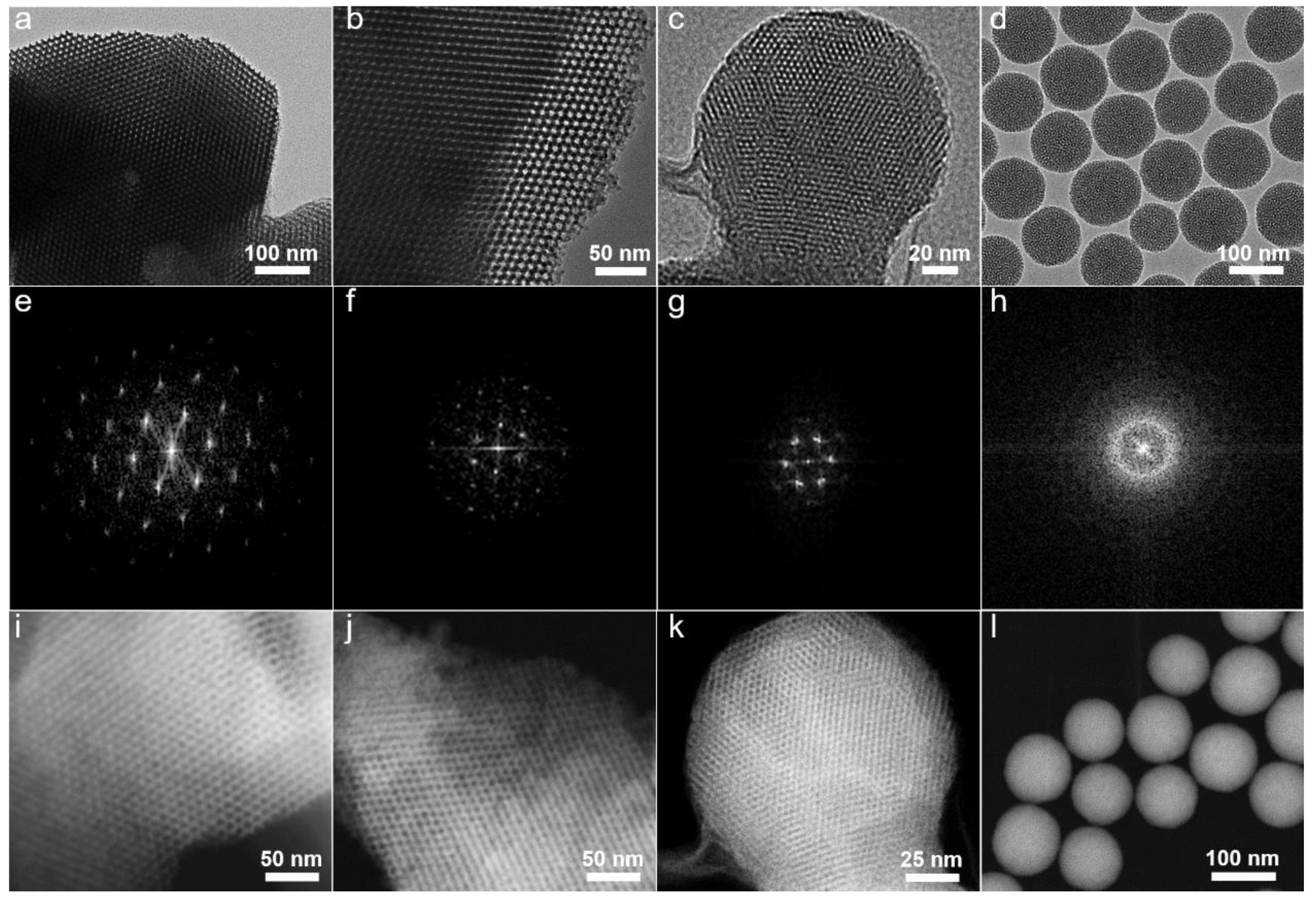
Figure 2.
Dependence of surface details on accelerating voltage. a~c Monte Carlo simulations of 2000 electrons with 15 keV, 2.5 keV and 500 eV kinetic energy are vertically incident to carbon, d~f SEM images of a TEM copper grids with accelerating voltage are 15 kV, 2.5 kV and 500 V.
Figure 2.
Dependence of surface details on accelerating voltage. a~c Monte Carlo simulations of 2000 electrons with 15 keV, 2.5 keV and 500 eV kinetic energy are vertically incident to carbon, d~f SEM images of a TEM copper grids with accelerating voltage are 15 kV, 2.5 kV and 500 V.
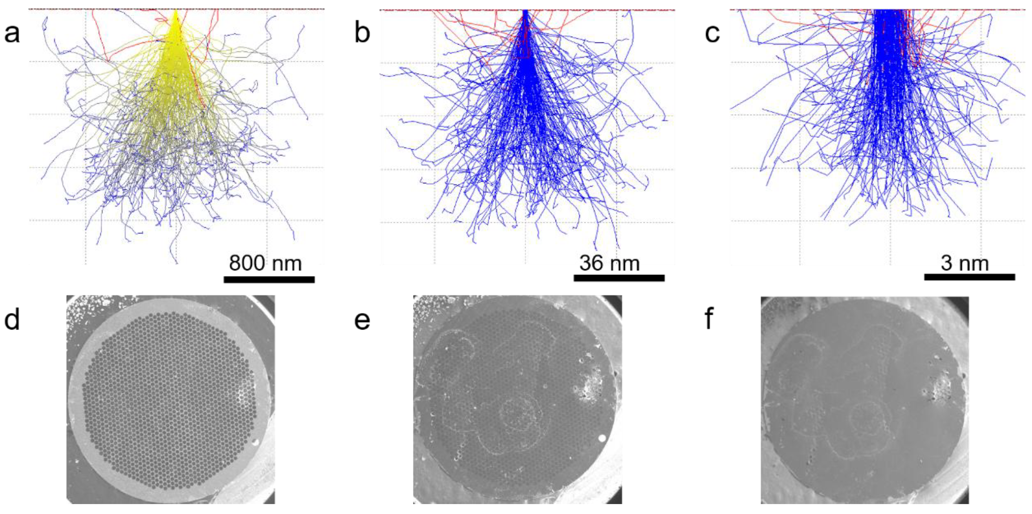
Figure 3.
Schematic of the three kinds of low voltage technologies. a directly low voltage, b stage bias beam deceleration, c in-column beam deceleration.
Figure 3.
Schematic of the three kinds of low voltage technologies. a directly low voltage, b stage bias beam deceleration, c in-column beam deceleration.
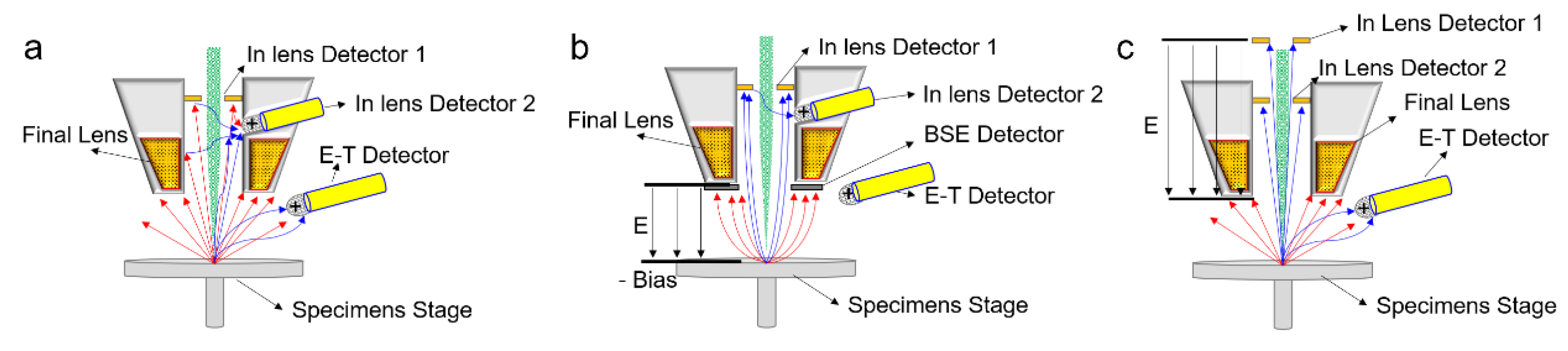
Figure 4.
Figure 4. LVSEM images of SBA-15 and KIT-6. SBA-15 by integrate concentric annular in-lens detector and side position in-lens detector with -3.5 kV stage bias (a, b), KIT-6 (c, d) by concentric annular in-lens detector coupled with 8 kV in-column beam deceleration, landing energy = 500 eV.
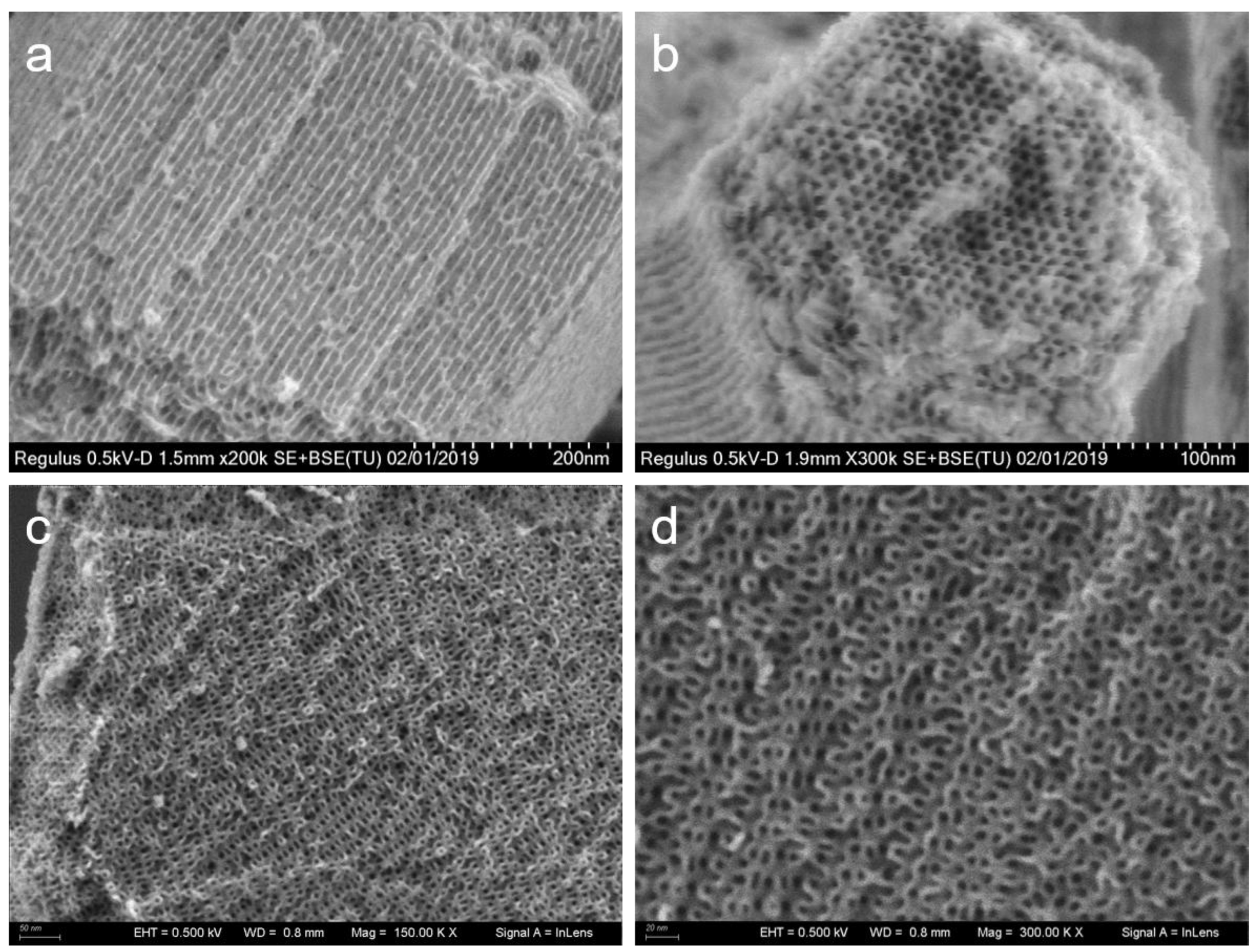
Figure 5.
LVSEM images of MSNSs and MCM-41. MSNSs by concentric annular in-lens detector coupled with 8 kV in-column beam deceleration, (a, b), MCM-41 (c, d) by integrate concentric annular in-lens detector and side position in-lens detector with -3.5 kV stage bias, landing energy = 500 eV.
Figure 5.
LVSEM images of MSNSs and MCM-41. MSNSs by concentric annular in-lens detector coupled with 8 kV in-column beam deceleration, (a, b), MCM-41 (c, d) by integrate concentric annular in-lens detector and side position in-lens detector with -3.5 kV stage bias, landing energy = 500 eV.
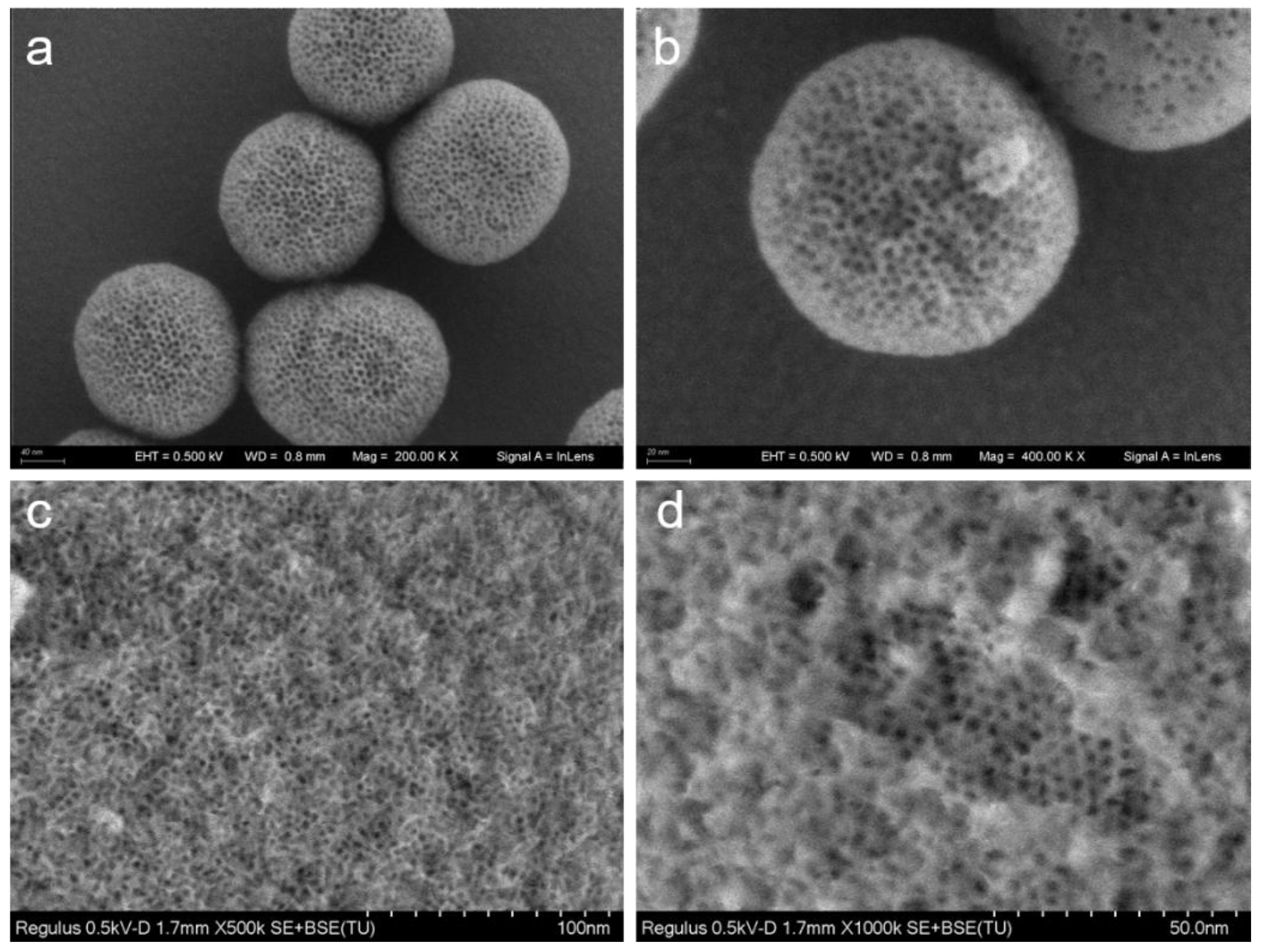
Figure 6.
200 kV high voltage SEM image of MCM-41. a a 200 kV secondary electrons image of MCM-41, b HAADF-STEM simultaneous image of MCM-41, c, d Monte Carlo simulations of 2000 electrons with 200 keV kinetic energy are vertically incident to a 100 nm SiO2 membrane supported by carbon.
Figure 6.
200 kV high voltage SEM image of MCM-41. a a 200 kV secondary electrons image of MCM-41, b HAADF-STEM simultaneous image of MCM-41, c, d Monte Carlo simulations of 2000 electrons with 200 keV kinetic energy are vertically incident to a 100 nm SiO2 membrane supported by carbon.
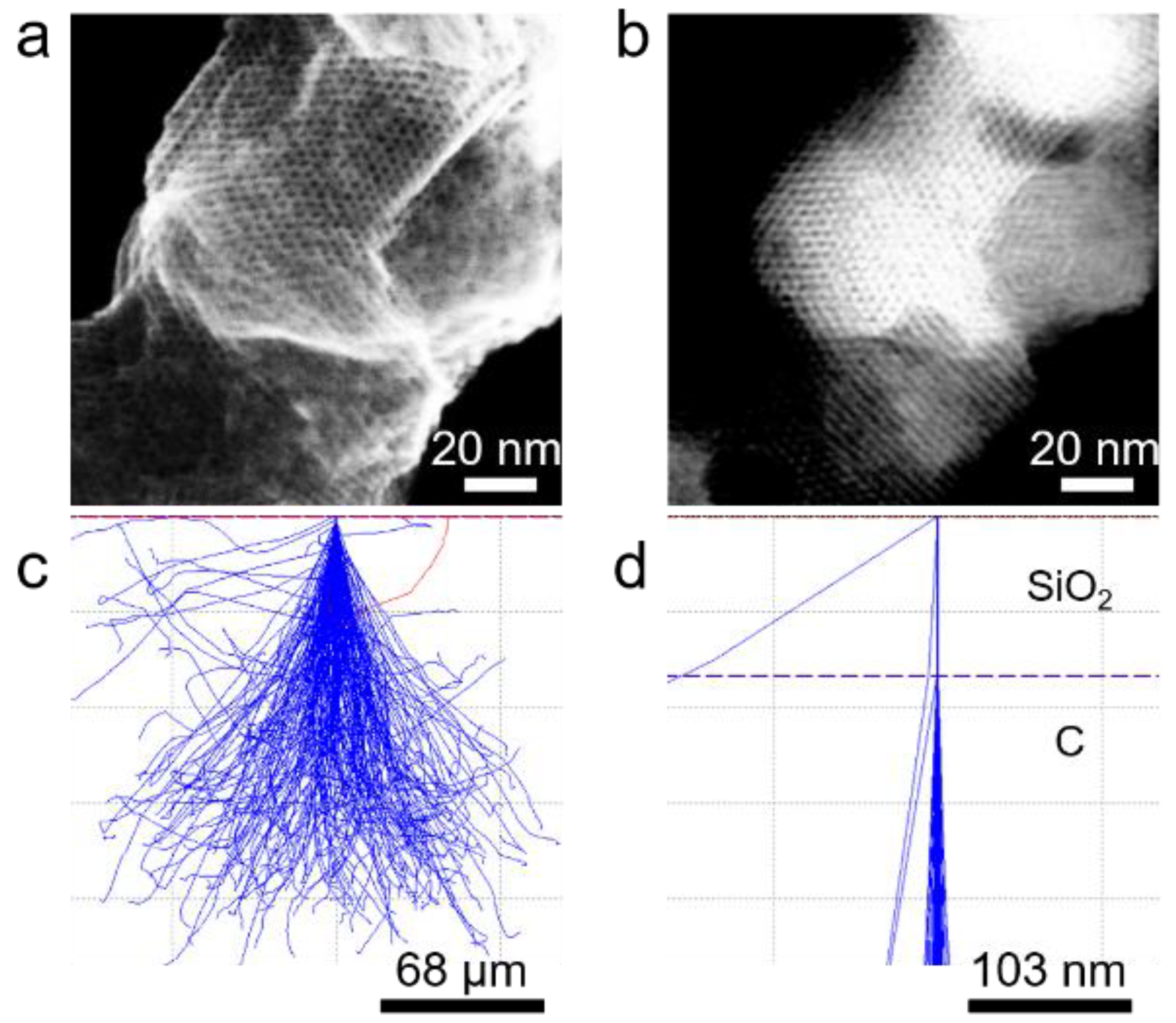

Table 1.
Texture Parameters of SBA-15, KIT-6, MSNSs and MCM-41 by BET and XRD Method.
| Sample | SBET m2g−1 | VT cm3g−1 | pore size nm | d(100) nm | wall thickness nm |
| SBA-15 | 757 | 0.958442 | 6.67 | 9.78 | 4.29 |
| KIT-6 | 499 | 1.18 | 6.64 | 9.84 | 2.75 |
| MSNSs | 575 | 0.45371 | 3.16 | 5.27 | 2.93 |
| MCM-41 | 1164 | 0.546457 | 2.00 | 3.74 | 1.74 |
Disclaimer/Publisher’s Note: The statements, opinions and data contained in all publications are solely those of the individual author(s) and contributor(s) and not of MDPI and/or the editor(s). MDPI and/or the editor(s) disclaim responsibility for any injury to people or property resulting from any ideas, methods, instructions or products referred to in the content. |
© 2025 by the authors. Licensee MDPI, Basel, Switzerland. This article is an open access article distributed under the terms and conditions of the Creative Commons Attribution (CC BY) license (http://creativecommons.org/licenses/by/4.0/).
Copyright: This open access article is published under a Creative Commons CC BY 4.0 license, which permit the free download, distribution, and reuse, provided that the author and preprint are cited in any reuse.


