Preprint
Article

This version is not peer-reviewed.

The Effect of Co/TiN Interfaces on the Co Interconnect Resistivity

A peer-reviewed article of this preprint also exists.

Submitted:

21 October 2025

Posted:

21 October 2025

You are already at the latest version

Abstract

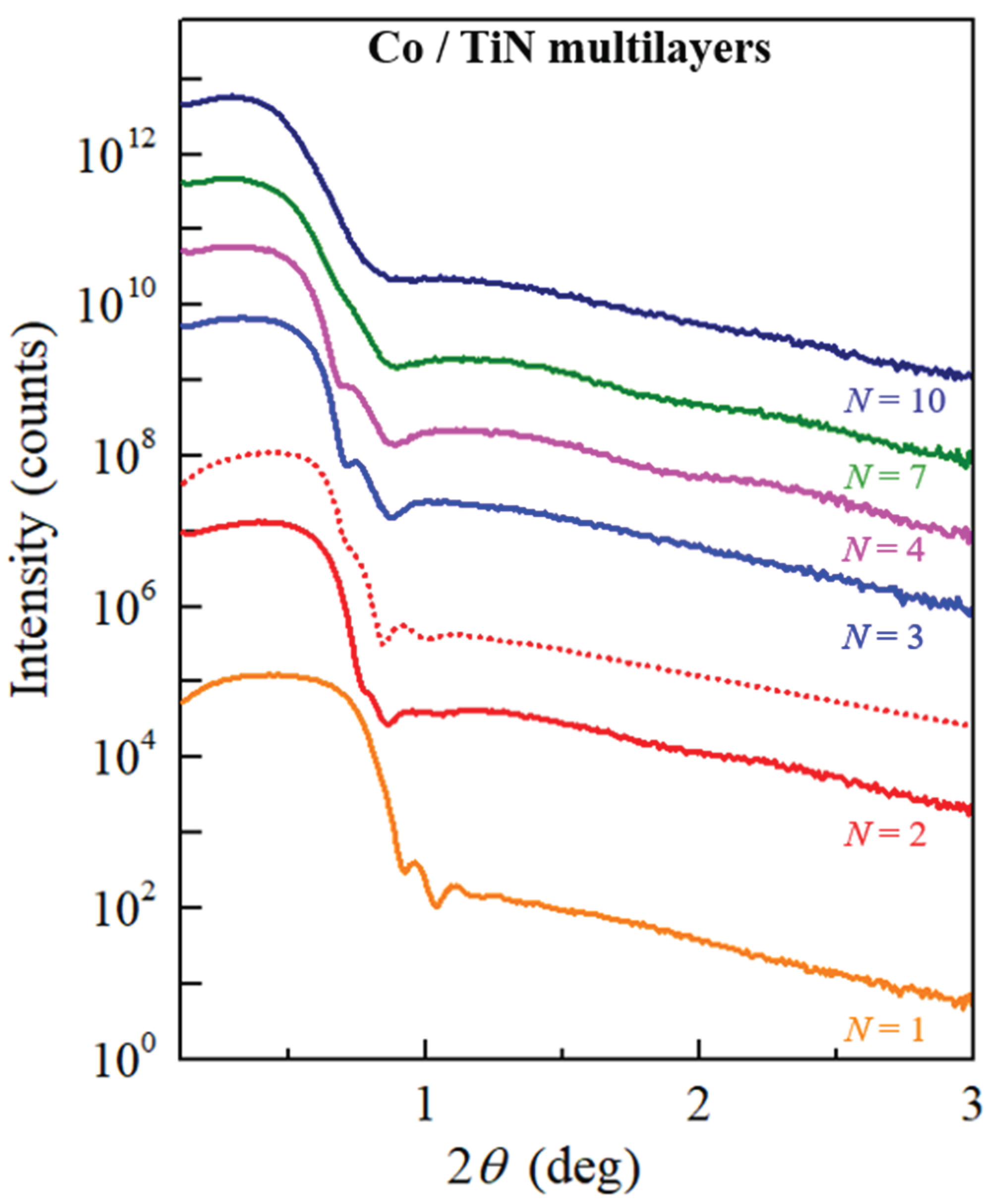
Electron transport measurements on Co/TiN multilayers are employed to explore the effect of TiN layers on the Co resistivity. 50-nm-thick multilayer stacks containing N = 1-10 individual Co layers that are separated by 1-nm-thick TiN layers are sputter deposited on SiO2/Si(001) substrates at 400 °C. X-ray diffraction and reflectivity measurements indicate a tendency for a 0001 preferred orientation, an x-ray coherence length of 13 nm that is nearly independent of N, and an interfacial roughness that increases with N. The in-plane multilayer resistivity ρ increases with increasing N = 1-10, from ρ = 14.4 to 36.6 µΩ-cm at room temperature and from ρ = 11.2 to 19.4 µΩ-cm at 77 K. This increase is due to a combination of increased electron scattering at interfaces and grain boundaries, as quantified using a combined Fuchs-Sondheimer and Mayadas-Shatzkes model. The analysis indicates that a decreasing thickness of the individual Co layers dCo from 50 to 5 nm causes not only an increasing resistivity contribution from Co/TiN interface scattering (from 9 to 88% with respect to the room temperature bulk resistivity), but also an increasing (39 to 154%) grain boundary scattering contribution which exacerbates the resistivity penalty due to the TiN liner. These results are supported by Co/TiN bilayer and trilayer structures deposited on Al2O3 (0001) at 600 °C. Interfacial intermixing causes Co2Ti and Co3Ti alloy phase formation, an increase in the contact resistance, a degradation of the Co crystalline quality, and a 2.3× higher resistivity for Co deposited on TiN than Co directly deposited on Al2O3(0001). The overall results show that TiN liners cause a dramatic increase in Co interconnects due to diffuse surface scattering, interfacial intermixing/roughness, and Co grain renucleation at Co/TiN interfaces.

Keywords: 
;  ;  ;  ;  

1. Introduction

A major challenge for the continued miniaturization of features in integrated circuits is the rise in signal delay and power consumption caused by an increasing interconnect resistance [1,2,3]. This resistance increase is due to diminishing conductor dimensions, resulting in a decreasing ratio of the cross-sectional area over the wire length. The decreasing conductor dimensions also cause the resistivity size effect [2,3,4], which refers to a resistivity increase at reduced dimensions due to electron scattering at surfaces [5,6,7,8,9,10], interfaces [11,12,13,14,15], and grain boundaries [6,16,17,18]. Extensive ongoing materials research focuses on quantifying the resistivity size effect for different conductors to evaluate their potential to provide a conductance benefit for highly scaled interconnects [19,20,21,22,23]. Interconnect research also includes the liner layer, which is designed to increase the adhesion between the conductor and the dielectric or diffusion barrier [24,25], and is important for interconnect reliability [26,27]. The liner affects the interconnect resistance in multiple ways: (i) It alters the electron scattering specularity p at the conductor liner interface [9,28,29] which, in turn, affects the conductor resistivity as described by the classical Fuchs and Sondheimer (FS) model [30,31]. (ii) The liner occupies a considerable fraction of the cross-sectional area of the trench used for the interconnect line, resulting in a higher resistance and an exacerbated resistivity size effect, motivating the development of particularly thin liner solutions [1,8,32,33]. (iii) The interconnect stack includes contacts between vertical (via) and horizontal (line) interconnects which typically are separated by a liner layer such that the current needs to flow across a high-resistance conductor-liner-conductor interface, motivating high-conductivity liners [34]. (iv) The liner acts as nucleation layer for subsequent conductor deposition and, therefore, affect the conductor microstructure and in particular the grain size and orientation distribution which contribute to the resistivity size effect [6,16]. Our present study explores the effects (i)-(iv) for the Co (conductor) and TiN (liner) material system.
Cobalt (Co) is a potential Cu replacement metal [35] due to its relatively low predicted product of the bulk resistivity times the bulk electron mean free path ρo × λ = 7.3/4.8×10-16 Ωm2 [3,20,33,34,36], which promises a relatively low resistivity size effect. In addition, the high melting point and cohesive energy in comparison to Cu promises a higher reliability against electromigration and time-dependent dielectric breakdown [26,37,38], and facilitates integration with relatively thin TiN liner layers [39]. TiN is expected to result in diffuse (p = 0) electron scattering at the Co/TiN interfaces [12] but the relatively low TiN resistivity [40,41] is expected to provide a high Co-TiN-Co interface conductivity. In addition, TiN has been demonstrated as a wetting layer for growth of Cu and Ag [12,42] and may similarly also aid Co deposition and increase the Co grain size, resulting in increased Co interconnect conductivity.
In this paper, we employ transport measurements on Co/TiN multilayer thin films to explore the effect of Co/TiN interfaces on the resistivity of Co. The multilayers consist of alternating Co and TiN layers, using a constant TiN thickness of 1 nm for all samples, representing a typical TiN liner thickness. The number of individual Co layers is varied from N = 1-10, and the Co layer thickness is varied from dCo = 50-5 nm, such that the total nominal Co thickness for all samples is kept constant at 50 nm. The resistivity of the superlattices parallel to the Co/TiN interfaces increases with increasing N, which is attributed to both increasing electron scattering at Co/TiN interfaces as well as a decreasing Co grain size caused by Co renucleation on each TiN interlayer.

2. Materials and Methods

Co/TiN multilayers were deposited on SiO2/Si(001) and Al2O3(0001) wafers in an ultra-high vacuum DC magnetron sputter deposition system with a base pressure of 10-9 Torr [43,44]. The 10×10 mm2 substrates consist of (i) a 100-nm thick SiO2 layer that was deposited on Si(001) by plasma-enhanced chemical vapor deposition, forms a smooth amorphous surface and electrically insulates the multilayers from the Si wafers, or (ii) single-crystal Al2O3(0001) which facilitates epitaxial growth of Co(0001) or TiN(111). The substrates were cleaned in subsequent ultrasonic baths of Hellmanex solution, acetone, isopropyl alcohol, and de-ionized water for 15 mins each, attached to a molybdenum block with colloidal silver paint, inserted into the deposition system through a load lock, and degassed in vacuum at 800 °C for one hour, using a radiative pyrolytic graphite heater. The substrate temperature was then reduced to 400 °C (or 600 °C for deposition on Al2O3(0001)), which was chosen to maximize multilayer crystalline quality and minimize Co-TiN intermixing, as quantified by x-ray diffraction and reflectivity. Depositions were done using 5-cm-diameter 99.99% pure Co and 99.995% pure Ti targets which were facing a continuously rotating substrate at a 12 cm distance and at -45° and 45° tilts. They were sputter cleaned prior to deposition for 10 min with closed shutters. Subsequently, the shutters in front of the Co and Ti targets were alternately opened and closed, and inlet valves for processing gas were simultaneously switched to obtain 10 mTorr 99.999% pure Ar or 7.5 mTorr 99.999% pure N2, for Co and TiN depositions, respectively, yielding the desired multilayers. Constant dc powers of 200 and 50 W to the Co and Ti targets resulted in deposition rates of 0.083 and 0.087 nm/s for Co and TiN, respectively. The bottom layer for all multilayers was a 1-nm-thick TiN layer, which facilitates Co-wetting on SiO2 and also reduces the possibility for Co diffusion into or reaction with the substrate. Different multilayers with different individual Co layer thicknesses dCo = 5-50 nm were deposited by adjusting the Co-deposition time from 60 to 600 s, while the TiN deposition time was kept constant at 11s for all TiN layers, yielding a constant TiN thickness of 1.0 nm. The number of multilayer periods N = 1-10 was varied in such a way that the total amount of Co for each multilayer was the same nominal 50 nm. For example, the N = 1 sample consists of one 50-nm-thick Co layer on top of one 1-nm-thick TiN layer, while the N = 10 sample consists of ten 5-nm-thick Co layers, separated by 1-nm-thick TiN layers. In addition, 75-nm-thick TiN/Co bilayers and trilayers were deposited on Al2O3(0001) at 600 °C such that the total amount of TiN (45 nm) and Co (30 nm) were kept constant. This included stacks with (i) 45-nm-thick TiN on top of 30-nm-thick Co, (ii) 30-nm-thick Co on top of 45-nm-thick TiN, and (iii) 22.5-nm-thick TiN on top of 30-nm-thick Co on top of 22.5-nm-thick TiN.
X-ray diffraction (XRD) analyses were performed using a PANalytical X'pert PRO MPD system with a λ = 1.5418 Å Cu source. Symmetric θ- scans were acquired with a fixed 0.5° divergence slit and a PIXcel solid-state line detector operating in scanning mode with a 14 mm active length corresponding to 255 active channels. Grazing incidence x-ray diffraction (GIXRD) scans were collected using a parabolic mirror yielding a parallel beam with a < 0.055° divergence, the PIXcel detector with a 3.3 mm active length, and a constant incidence angle ω = 2°. The latter was chosen to maximize the thin film XRD peak intensity while ensuring that diffracted intensity is detected from the whole layer thickness. ω rocking curves of Co 0002 reflections were obtained using the same parabolic mirror, a fixed = 44.38° and the line detector operating in receiving mode with a 0.165 mm active length. X-ray reflectivity (XRR) scans were acquired with the same parallel beam geometry with the line detector operating in receiving mode with a 0.165 mm active length. The measured XRR data were fitted using the PANalytical X’Pert Reflectivity software which employs the Parratt formalism, following the procedure of our previous work on multilayers [13,14,44,45]. The model for data fitting included alternating TiN and Co layers on SiO2, with densities fixed at literature values of 5.4, 8.9, and 2.65 g/cm3, respectively. The free fitting parameters were the thickness of each layer within the multilayer stack and the roughness of each interface and top surface.
The multilayer sheet resistances were measured in air at 293 K with a linear four-point-probe with spring loaded tips and a 1.0 mm inter-probe spacing. Measurements at 77 K were taken with the same linear four-point probe with both sample and probe tips completely immersed in liquid nitrogen. The resistivity was determined from the measured sheet resistance using the measured thickness and the appropriate geometric correction factor [46].

3. Results and Discussion

Figure 1 shows typical X-ray reflectivity patterns from Co/TiN multilayer films consisting of N = 1, 2, 3, 4, 7 or 10 Co and TiN layers, as labeled. The measured intensity is plotted as solid lines in a logarithmic scale as a function of the scattering angle 2θ = 0.1-3° and offset by factors of 10 for clarity purposes. The plot includes as dotted line the typical result from curve fitting for N = 2. The N = 1 sample consists of a single Co layer on top of a 1-nm-thick TiN layer on SiO2/Si(001). Its pattern shows a critical angle 2θ = 0.51° ± 0.02°, close to the expected 0.48° for pure Co with a density of 8.9 ± 0.1 g/cm3. The pattern also shows thickness fringes near 2θ = 0.95° and 1.11°, indicating a Co thickness of 55.2 nm, in reasonable agreement with the nominal 50 nm. The N = 2 sample shows a qualitatively similar pattern. However, its critical angle 2θ = 0.47° ± 0.02° is moved to a slightly lower angle and the fringes are less pronounced, which is attributed to a relatively high interface and surface roughness. More specifically, the data fitting for this sample (red dotted line) indicates a multilayer with two Co-layers with a 4.1 nm interface roughness. The patterns from the multilayers with increasing N = 3, 4, 7 and 10 indicate a continued decrease in the critical angle to 2θ = 0.45°, 0.40°, 0.34° and 0.32°. This is attributed to a decreasing effective overall multilayer density associated with an increasing volume fraction of the lower-density TiN within the multilayer in combination with the possible development of an underdense microstructure associated with Co renucleation at each TiN interface, leading to a decreasing grain size with increasing N, as discussed below. In addition, the fringes near 2θ = 1° become less pronounced for N = 3 and 4, and cannot be detected for N = 7 and 10. This indicates an increasing Co/TiN interface roughness with increasing N. The patterns from the N = 4, 7, and 10 multilayers exhibit broad (weak) features with maxima at 1.3° and 2.4° which are attributed to superlattice fringes [13,44]. Data fitting cannot uniquely determine the associated superlattice periods (nominally: 13.5, 8.1, and 6.0 nm) from these fringes due to their low intensity above the background noise.
Figure 2 shows grazing incidence x-ray diffraction θ-2θ patterns from six 50-nm-thick Co/TiN multilayer films containing N = 1, 2, 3, 4, 7 and 10 Co layers. The measured intensity is plotted in a linear scale and the patterns are offset for clarity purposes. The N = 1 pattern shows a relatively strong peak at 2θ = 44.5° due to the Co 0002 reflection. Other possible peaks from Co 10 1 ¯ 0 and Co 10 1 ¯ 1 would be expected at 2θ = 41.6° and 47.4° for a random crystalline orientation. However, they have insufficient intensity to be distinguishable from the background noise. This suggests a tendency for a 0001 preferential crystalline orientation of the Co layer, since the expected 10 1 ¯ 0 peak intensity from Co with randomly oriented grains is similar to the 0002 intensity, while the Co 10 1 ¯ 1 reflection for randomly oriented grains is even expected to be four times stronger than the Co 0002 (JCPDS Card No. 01-071-4239). We note that the 0001 out-of-plane crystalline alignment is relatively weak since GIXRD measures the 0001 planes with a 20° tilt with respect to the surface normal and symmetric XRD θ-2θ scans (not shown) could not detect any Co peaks due to low intensity, suggesting considerable grain misalignment in combination with a small grain size and/or low crystalline quality. Increasing the number of Co layers to N = 2, 3, 4, 7 and 10 results in qualitatively and quantitatively similar GIXRD patterns, indicating that the degree of crystalline alignment is independent of the number of Co/TiN interfaces, which is important for the interpretation of the transport results presented below. This is further illustrated in the inset of Figure 2, which shows higher resolution and higher signal-to-noise ratio GIXRD scans of the Co 0002 peak from the N = 1 and N = 10 samples. Their full width at half-maximum (FWHM) peak widths of σ = 0.70° and 0.73° are nearly identical. This corresponds to x-ray coherence lengths ξ = λ/(σ cos θ) = 13.1 and 13.6 nm, respectively. These coherence lengths measured by GIXRD are for a direction perpendicular to the 0001 planes, that is at a 20° tilt with respect to the surface normal. We note that ξ is larger than the dCo = 5 nm Co layer thickness for the N = 10 sample, indicating that crystalline grains are larger (approximately along the growth direction) than individual Co layers, suggesting that the Co/TiN interfaces exhibit local epitaxy or the nominally 1-nm-thick TiN layers are not continuous such that Co grains may extend across 2-3 layers. This suggests some Co-TiN interfacial intermixing, which is consistent with the interface roughness > 4 nm measured by XRR.
Figure 3 is a plot of the resistivity ρ of Co/TiN multilayers vs the thickness dCo of individual Co layers within the multilayers. The blue triangle and red square data points are the resistivity measured at 77 and 293 K, respectively, and the lines through the data points are the result from curve fitting using a combined Fuchs-Sondheimer and Mayadas-Shatzkes model, as discussed below. The room temperature resistivity decreases from ρ = 36.6 µΩ-cm for dCo = 5.1 nm to ρ = 30.9, 26.9, 25.5, 19.6 and 14.4 µΩ-cm for dCo = 7.3, 12.8, 17.0, 25.5 and 51.0 nm, corresponding to multilayer films with N = 10, 7, 4, 3, 2, and 1 Co layers, respectively. The resistivity at 77 K shows a similar decrease with increasing dCo, from 24.6 to 21.3, 17.0, 14.0, 11.4 and 6.9 µΩ-cm. These values are lower than at 293 K, which is due to the reduced electron phonon scattering at low temperatures. The resistivity difference Δρ between the two plotted data sets in Figure 3 decreases from 12.0 to 7.5 µΩ-cm with increasing dCo, indicating that Matthiessen’s rule for additive resistivity contributions from electron-phonon and other scattering processes does not apply to our Co/TiN multilayers. The average measured Δρ = 9.8 μΩ-cm is 67% larger than the reported Δρ = 5.82 µΩ-cm for bulk Co, based on ρ = 6.37 µΩ-cm at 293 K and ρ = 0.55 µΩ-cm at 77 K. The larger Δρ for the multilayers are likely due to a reduction in the effective cross-sectional area of conducting Co caused by Co/TiN interfacial intermixing. More importantly, all multilayers have resistivities that are well above the reported bulk values. This is attributed to electron scattering at Co/TiN interfaces and at grain boundaries as quantitatively discussed in the following.
We describe the measured ρ vs dCo in our multilayers using a parallel conductor model, where each Co layer acts as an individual conductor such that the multilayer resistivity becomes identical to the resistivity of each individual Co layer. This approach neglects the electron transport in the TiN interlayers as well as their thickness, which are expected to be negligible as discussed before. The resistivity of an individual Co layer with thickness dCo is described by a combined Fuchs-Sondheimer (FS) [30,47] and Mayadas-Shatzkes (MS) [48] model for surface and grain boundary scattering, respectively, yielding the approximate expression:
ρ C o = ρ o + ρ o λ C o 3 4 d C o 1 p + ρ o λ C o 3 R 2 D ( 1 R )
This equation contains multiple correlated parameters which cannot all be independently determined by direct data fitting. Thus, for the data analysis in this paper, we fix all parameters based on previously reported values with the exception of the grain size D, which is determined by the fitting procedure. More specifically, the bulk resistivity ρo is kept fixed at 0.55 and 10.34 µΩ-cm for 77 and 293 K, respectively, where the former is the reported bulk resistivity ρo,77K at 77 K [38] and the latter is the sum of ρo,77K plus our measured average Δρ = 9.79 μΩ-cm due to phonon scattering, as discussed above. The probability p for specular scattering at the Co/TiN interfaces is set to zero for all samples and at all temperatures, assuming completely diffuse interface scattering, based on the reported diffuse electron scattering at Co-TiN interfaces [15]. The product of bulk resistivity times electron mean free path ρo×λCo is fixed to the previously reported value of 12.2 ×10⁻¹⁶ Ωm2 [22], which is independent of temperature and corresponds to a Co bulk electron mean free paths λCo = 11.7 nm at room temperature and λCo = 220 nm at 77 K. The average electron grain boundary reflection probability in Co is set to R = 0.3 for all samples and temperatures, based on previously reported studies [49,50,51,52]. The solid blue and red lines in Figure 3 are the result from curve fitting to the 77 and 293 K data. This is done using Eq. (1) with the above discussed fixed parameters while the grain size D is the only free fitting parameter. D is expected to increase with dCo, following a power law DdCon as common for polycrystalline film growth [53]. Thus, our fitting procedure includes (i) estimation of D using Eq. (1) for each sample and temperature, (ii) taking the average of the estimated D at 77 and 293 K for each given sample, and (iii) curve fitting of these average D values with the power law. This process yields a growth exponent n = 0.4, matching typical values for thin film deposition at relatively low homologous temperatures [53] as is the case for Co deposition at Ts = 400 °C with a melting point Tm = 1495 °C, corresponding to a homologous temperature of 0.38. The resulting grain size increases (as expected) monotonously with increasing dCo from 4.9 nm for dCo = 5.1 nm to D = 19.7 nm for dCo = 51 nm. The blue and red curves in Figure 3 describe the measured data well, indicating that Eq. (1) which accounts for both interface and grain boundary scattering can simultaneously describe the low temperature and room temperature resistivity. We note that additional microstructural features such as interface roughness or interfacial intermixing may also contribute to the resistivity but are not explicitly accounted for in Eq. (1). That is, they are effectively accounted for by the surface and grain boundary scattering terms which, in turn, become “effective” scattering contributions. More quantitatively, surface and grain boundary scattering contribute 9.1 and 15.9 µΩ-cm to the room temperature resistivity of the dCo = 5.1 nm sample, corresponding to 88% and 154% of 10.34 µΩ-cm due to bulk scattering. In contrast, the corresponding values for the dCo = 51 nm sample are only 9% and 39%. These values demonstrate the large effect that TiN liners can have on the Co resistivity and that this effect is not only due to diffuse surface scattering but also compounded by Co renucleation at the Co/TiN interfaces, resulting in a small Co grain size and a correspondingly large resistivity contribution from grain boundary scattering.
Figure 4 shows x-ray diffraction θ-2θ patterns from two bilayer and one trilayer stacks deposited on Al2O3(0001) at 600 °C. Each stack has a total thickness of 75 nm and their layer sequence is illustrated in the schematics on the right. The measured intensity is plotted on a logarithmic scale and the patterns are offset by factors of 10 for clarity purposes. All three patterns show a double-peak feature at 2θ = 41.70° and 41.80° due to the Al2O3 0006 substrate reflections of the CuKα1 and CuKα2 lines. The red pattern from the bilayer structure with 45 nm TiN on top of 30 nm Co shows a peak at 2θ = 44.38° which is attributed to Co 0002 and corresponds to an out-of-plane lattice parameter of 0.4081 nm. The blue pattern from the Co/TiN/Al2O3(0001) sample shows peaks at 2θ = 36.85° and 44.31° which are attributed to TiN 111 and Co 0002 reflections. The Co 0002 peak intensity is half as strong as that from the TiN/Co/Al2O3(0001) sample, indicating a degradation in the cobalt crystalline quality and/or 0001 crystalline alignment when Co is deposited on TiN 111 instead of directly on Al2O3(0001). The pink pattern from the trilayer stack where 30 nm of Co is sandwiched between two 22.5-nm-thick TiN layers shows the same TiN 111 and Co 0002 peaks at 2θ = 36.92° and 44.31. The TiN 111 peak intensity is as strong as the TiN 111 reflection from the Co/TiN/Al2O3(0001) sample, but the Co 0002 intensity is 3 times weaker than for the Co/TiN/Al2O3(0001) sample, indicating a further Co crystal degradation after depositing a TiN layer on the top. Two additional peaks at 2θ = 37.31° and 43.59 are attributed to 022 and 111 reflections from the intermediate alloys Co2Ti and Co3Ti, respectively [54]. This suggests an increased level of Co-Ti intermixing which is attributed to the presence of two Co/TiN interfaces in the trilayer structure. The inset in Figure 4 shows a Co 0002 ω-rocking curve from the TiN/Co/Al2O3(0001) bilayer, obtained using 2θ = 44.50° corresponding to the Co 0002 peak position. The peak has a FWHM of 0.05°, indicating strong Co[0001] crystal alignment along the growth direction, consistent with previous reports on the epitaxial growth of Co(0001)/Al2O3(0001) [38,55]. We note that comparable measurements on the other two samples does not yield sufficient signal-to-noise ratio to determine the rocking curve width, consistent with the lower intensity of the Co 0002 peaks in the θ-2θ scans, and the corresponding lower crystalline quality and crystalline alignment.
Table 1 shows the measured sheet resistances Rs from the three 75-nm bilayer and trilayer samples discussed above, and also from a single 45-nm-thick TiN/Al2O3(0001) and a single 30-nm-thick Co(0001)/Al2O3 (0001) layer. Rs = 23.8 Ω/sq from the TiN layer yields a resistivity ρTiN = 107 μΩ-cm for a TiN layer directly deposited on Al2O3(0001). Correspondingly, Rs = 3.3 from the Co layer yields a resistivity ρCo = 9.8 μΩ-cm for a Co(0001) layer directly deposited on Al2O3(0001).
We use these data in Table I to determine the amount of the intermixed alloy and the resistivity increment in the Cobalt layer due to TiN templating which results in crystalline quality degradation of the Co layer. For this purpose, a parallel conductor model is applied, where the total sheet conductance 1/Rs is the sum of the sheet conductance of the TiN layer, the Co layer and the interfacial alloy layer:
1 R s   = d T i N ρ T i N + d C o ρ C o + d a ρ a
Here, ρTiN, ρCo and ρ a are the resistivities of TiN, Co, and the interfacial alloy, while dTiN, dCo and da are the corresponding layer thicknesses, respectively. We note that ρTiN and ρCo are a function of the microstructure and depend on the underlaying layer. We assume that the interfacial intermixing causes an equal reduction of the thickness of adjacent TiN and Co layers. Thus, for bilayer structures dTiN = (45- da/2) nm and dCo = (30- da/2) nm, while the total thickness remains 75 nm. We first consider the bilayer sample TiN/Co/Al2O3(0001). The Co layer is directly deposited on the Al2O3(0001), such that we expect its resistivity to match that of the Co/Al2O3(0001), i.e. ρCo = 9.8 μΩ-cm. The resistivity of the interfacial alloy is fixed at ρ a = 145 μΩ-cm, based on the previously reported studies [56], while the resistivity of TiN which is deposited on top of Co is expected to be larger than that of TiN/Al2O3(0001) and within the large range of previously published TiN resistivities [57,58], such that ρTiN for this sample is between 107 and 300 μΩ-cm. Using an arbitrary “average” value of 200 μΩ-cm and solving Eq. 2 for the interfacial alloy thickness yields da = 24.8 nm. We note that there is a relatively large uncertainty in both at ρ a and ρTiN. However, because these resistivities are much larger than ρCo, the majority of the current is flowing through the Co layer and the calculated da is relatively unsensitive to the exact values for ρ a and ρTiN. For example, changing the TiN resistivity by 50 μΩ-cm to ρTiN = 150 or 250 μΩ-cm results in da = 26.0 or 24.1 nm, respectively, with both values within 1.2 nm from the calculated da = 24.8 nm.
We consider now the Co/TiN/Al2O3(0001) bilayer sample. Here the TiN layer is directly deposited on Al2O3(0001) such that it has an expected resistivity ρTiN = 107 μΩ-cm. In contrast, ρCo is unknown because it is deposited on TiN, which causes a degradation of the Co crystalline quality, as presented in Figure 4. However, it is reasonable to assume the same level of TiN-Co interfacial intermixing for the Co/TiN/Al2O3(0001) and the TiN/Co/Al2O3(0001) samples. Thus, we know from above da = 24.8 nm and the only unknown in Eq. (2) becomes ρCo. Solving for ρCo yields 22.7 μΩ-cm. This is 2.3× larger than ρCo = 9.8 μΩ-cm from Co directly deposited on Al2O3(0001). That is, the degradation in the crystallin quality of Co deposited on TiN results in a doubling of the Co resistivity, which is consistent with the steep resistivity increase with decreasing dCo shown in Figure 3.
Lastly, we consider the trilayer stack. Based on the analyses from the bilayers we set ρCo = 22.7 μΩ-cm, ρa = 145 μΩ-cm, and ρTiN = 107 and 200 μΩ-cm for the bottom and top TiN layers, respectively. The intermixing at the two TiN-Co interfaces is assumed to be equal to that of the TiN-Co interfaces in the bilayer structures. Therefore, da = 24.8 nm, dTiN = (22.5 - da/2) nm = 10.1 nm for both bottom and top TiN layers, and dCo = (30- da) nm = 5.2 nm. We note that the relative uncertainty in these numbers is large. In particular, these numbers suggest a negligible Co thickness of 5.2±2 nm, which is consistent with the weak XRD Co peak for this sample shown in Figure 4. Nevertheless, using these numbers and an expression similar to Eq. (2) yields an expected sheet resistance for the trilayer structure of 14.0 Ω/sq. This agrees (within 23%) with the measured Rs = 18.1 Ω/sq, indicating that the quantitative resistance analyses are successful.

4. Conclusions

Co/TiN multilayers are deposited on SiO2/Si(001) at 400 °C by sputtering alternating Co and Ti sources with Ar and N2 processing gases. X-ray reflectivity measurements indicate an increasing Co/TiN interface roughness with an increasing number of multilayer periods. X-ray diffraction measurements suggest that Co grains penetrate discontinuous nominally-1-nm-thick TiN layers. The multilayer resistivity increases with decreasing thickness of individual Co layers. This is caused by compounding effects from increasing interface and grain boundary scattering, resulting in a room-temperature resistivity that is 254% above that for bulk Co for dCo = 5.1 nm. Co/TiN bilayer and trilayer stacks deposited on Al2O3(0001) at 600 °C reveal Co/TiN interfacial intermixing and the formation of Co2Ti and Co3Ti alloy phases which cause a considerable increase in the contact resistance. In addition, Co deposited on TiN has a lower crystalline quality and a 2.3× higher resistivity than Co directly deposited on Al2O3(0001), confirming the negative impact of TiN liners on the Co conductivity. The overall results show that TiN liners cause a dramatic resistivity increase in Co interconnects due to diffuse surface scattering, interfacial intermixing/roughness, and Co grain renucleation at Co/TiN interfaces.

Data Availability

The data that supports the findings of this study are available within the article.

Acknowledgments

The authors acknowledge funding from the Semiconductor Research Corporation (SRC) under task 3085.001, SRC/DARPA under JUMP 2.0 center tasks 3137.019 and 3137.021, the National Science Foundation (NSF) under grant No. 2328906 through the Future of Semiconductors program supported by NSF and industry partners, and from the NY State Empire State Development's Division of Science, Technology and Innovation (NYSTAR) through Focus Center-NY–RPI Contract C210117.

Author Declarations

The authors have no conflicts to disclose.

References

  1. Kim, H. Recent Trends in Copper Metallization. Electronics 2022, 11, 2914. [Google Scholar] [CrossRef]
  2. Rossnagel, S.M.; Kuan, T.S. Alteration of Cu Conductivity in the Size Effect Regime. J. Vac. Sci. Technol. B 2004, 22, 240–247. [Google Scholar] [CrossRef]
  3. Gall, D. Metals for Low-Resistivity Interconnects. In Proceedings of the 2018 IEEE International Interconnect Technology Conference (IITC); IEEE, June 2018; pp. 157–159. [Google Scholar]
  4. Xu, W.H.; Wang, L.; Guo, Z.; Chen, X.; Liu, J.; Huang, X.J. Copper Nanowires as Nanoscale Interconnects: Their Stability, Electrical Transport, and Mechanical Properties. ACS Nano 2015, 9, 241–250. [Google Scholar] [CrossRef]
  5. Jog, A.; Zheng, P.; Zhou, T.; Gall, D. Anisotropic Resistivity Size Effect in Epitaxial Mo(001) and Mo(011) Layers. Nanomaterials 2023, 13, 957. [Google Scholar] [CrossRef]
  6. Jog, A.; Gall, D. Electron Scattering at Surfaces and Grain Boundaries in Rh Layers. IEEE Trans. Electron Devices 2022, 69, 3854. [Google Scholar] [CrossRef]
  7. Zhang, M.; Gall, D. Resistivity Size Effect in Epitaxial VNi2 Layers. J. Appl. Phys. 2023, 134, 105302. [Google Scholar] [CrossRef]
  8. Zhang, M.; Gall, D. CuTi as Potential Liner- and Barrier-Free Interconnect Conductor. IEEE Trans. Electron Devices 2024, 71, 3252–3257. [Google Scholar] [CrossRef]
  9. Zhou, T.; Gall, D. Resistivity Scaling Due to Electron Surface Scattering in Thin Metal Layers. Phys. Rev. B 2018, 97, 165406. [Google Scholar] [CrossRef]
  10. Reider, A.M.; Kronthaler, A.; Zappa, F.; Menzel, A.; Laimer, F.; Scheier, P. Comparison of Continuous and Pulsed Low-Power DC Sputtered Ti Thin Films Deposited at Room Temperature. Surfaces 2025, 8, 19–21. [Google Scholar] [CrossRef]
  11. Chawla, J.S.; Gall, D. Epitaxial Ag(001) Grown on MgO(001) and TiN(001): Twinning, Surface Morphology, and Electron Surface Scattering. J. Appl. Phys. 2012, 111, 043708. [Google Scholar] [CrossRef]
  12. Chawla, J.S.; Zhang, X.Y.; Gall, D. Epitaxial TiN(001) Wetting Layer for Growth of Thin Single-Crystal Cu(001). J. Appl. Phys. 2011, 110, 043714. [Google Scholar] [CrossRef]
  13. Shen, P.; Gall, D. Electron Scattering at Interfaces in Epitaxial W(001)-Mo(001) Multilayers. J. Appl. Phys. 2024, 136, 075305. [Google Scholar] [CrossRef]
  14. Shen, P.; Lavoie, C.; Gall, D. Electron Scattering at Interfaces in Ru(0001)/Co(0001) Multilayers. J. Appl. Phys. 2025, 137. [Google Scholar] [CrossRef]
  15. Milosevic, E.; Gall, D. Electron Scattering at Co(0001) Surfaces: Effects of Ti and TiN Capping Layers. AIP Adv. 2020, 10, 055213. [Google Scholar] [CrossRef]
  16. Zhou, T.; Jog, A.; Gall, D. First-Principles Prediction of Electron Grain Boundary Scattering in Fcc Metals. Appl. Phys. Lett. 2022, 120, 241603. [Google Scholar] [CrossRef]
  17. César, M.; Gall, D.; Guo, H. Reducing Grain-Boundary Resistivity of Copper Nanowires by Doping. Phys. Rev. Appl. 2016, 5, 054018. [Google Scholar] [CrossRef]
  18. Chawla, J.S.; Gstrein, F.; Brien, K.P.O.; Clarke, J.S.; Gall, D. Electron Scattering at Surfaces and Grain Boundaries in Cu Thin Films and Wires. Phys. Rev. B 2011, 84, 235423–1. [Google Scholar] [CrossRef]
  19. Jog, A.; Gall, D. Resistivity Size Effect in Epitaxial Iridium Layers. J. Appl. Phys. 2021, 130, 115103. [Google Scholar] [CrossRef]
  20. Zhang, M.; Gall, D. Resistivity Scaling in Epitaxial CuAl 2 (001) Layers. IEEE Trans. Electron Devices 2022, 69, 5110–5115. [Google Scholar] [CrossRef]
  21. Milosevic, E.; Kerdsongpanya, S.; Mcgahay, M.E.; Wang, B.; Gall, D. The Resistivity Size Effect in Epitaxial Nb(001) and Nb(011) Layers. IEEE Trans. Electron Devices 2019, 66, 3473–3478. [Google Scholar] [CrossRef]
  22. Gall, D. The Search for the Most Conductive Metal for Narrow Interconnect Lines. J. Appl. Phys. 2020, 127, 050901. [Google Scholar] [CrossRef]
  23. Zheng, P.; Gall, D. The Anisotropic Size Effect of the Electrical Resistivity of Metal Thin Films: Tungsten. J. Appl. Phys. 2017, 122, 135301. [Google Scholar] [CrossRef]
  24. Hu, C.K.; Gignac, L.; Rosenberg, R. Electromigration of Cu/Low Dielectric Constant Interconnects. Microelectron. Reliab. 2006, 46, 213–231. [Google Scholar] [CrossRef]
  25. Kaloyeros, A.E.; Eisenbraun, E. Ultrathin Diffusion Barriers/Liners for Gigascale Copper Metallization. Annu. Rev. Mater. Sci. 2000, 30, 363–385. [Google Scholar] [CrossRef]
  26. L. G. Wen, P. Roussel, O. V. Pedreira, B. Briggs, B. Groven, S. Dutta, M. I. Popovici, N. Heylen, I. Ciofi, K. Vanstreels, F. W. Østerberg, O. Hansen, D. H. Petersen, K. Opsomer, C. Detavernie, C. J. Wilson, S. V. Elshocht, K. Croes, J. Bömmels, Z.T.; Adelmann, C. Atomic Layer Deposition of Ruthenium with TiN Interface for Sub-10 Nm Advanced Interconnects beyond Copper. ACS Appl. Mater. Interfaces 2016, 8, 26119. [Google Scholar] [CrossRef]
  27. He, M.; Zhang, X.; Nogami, T.; Lin, X.; Kelly, J.; Kim, H.; Spooner, T.; Edelstein, D.; Zhao, L. Mechanism of Co Liner as Enhancement Layer for Cu Interconnect Gap-Fill. J. Electrochem. Soc. 2013, 160, D3040–D3044. [Google Scholar] [CrossRef]
  28. Zheng, P.; Zhou, T.; Gall, D. Electron Channeling in TiO2 Coated Cu Layers. Semicond. Sci. Technol 2016, 31, 055005. [Google Scholar] [CrossRef]
  29. Zheng, P.Y.; Deng, R.P.; Gall, D. Ni Doping on Cu Surfaces: Reduced Copper Resistivity. Appl. Phys. Lett. 2014, 105, 131603. [Google Scholar] [CrossRef]
  30. Sondheimer, E.H. The Mean Free Path of Electrons in Metals. Adv. Phys. 1952, 1, 1–42. [Google Scholar] [CrossRef]
  31. Lucas, M.S.P. Electrical Conductivity of Thin Metallic Films with Unlike Surfaces. J. Appl. Phys. 1965, 36, 1632–1635. [Google Scholar] [CrossRef]
  32. Nies, C.L.; Natarajan, S.K.; Nolan, M. Control of the Cu Morphology on Ru-Passivated and Ru-Doped TaN Surfaces-Promoting Growth of 2D Conducting Copper for CMOS Interconnects. Chem. Sci. 2022, 13, 713–725. [Google Scholar] [CrossRef]
  33. D. Gall, J. J. Cha, Z. Chen, H. J. Han, C. Hinkle, J.A. Robinson, R. Sundararaman, R. Torsi Materials for Interconnects. MRS Bull. 2021, 46, 959. [Google Scholar] [CrossRef]
  34. Zhou, T.; Lanzillo, N.A.; Bhosale, P.; Gall, D.; Quon, R. A First-Principles Analysis of Ballistic Conductance, Grain Boundary Scattering and Vertical Resistance in Aluminum Interconnects. AIP Adv. 2018, 8, 055127. [Google Scholar] [CrossRef]
  35. Mont, F.W.; Zhang, X.; Wang, W.; Kelly, J.J.; Standaert, T.E.; Quon, R.; Ryan, E.T. Cobalt Interconnect on Same Copper Barrier Process Integration at the 7nm Node. In Proceedings of the 2017 IEEE International Interconnect Technology Conference (IITC); IEEE, May 2017; pp. 1–3. [Google Scholar]
  36. Thakral, A.; Jog, A.; Gall, D. Resistivity Size Effect in Epitaxial Face-Centered Cubic Co(001) Layers. Appl. Phys. Lett. 2024, 124, 121601. [Google Scholar] [CrossRef]
  37. Zhang, D.; Xu, J.; Mao, S.; Zhao, C.; Wang, G.; Luo, X.; Li, J.; Li, Y.; Wang, W.; Chen, D.; et al. Co-Sputtering Co–Ti Alloy as a Single Barrier/Liner for Co Interconnects and Thermal Stability Enhancement Using TiN Metal Capping. J. Mater. Sci. Mater. Electron. 2019, 30, 10579–10588. [Google Scholar] [CrossRef]
  38. Milosevic, E.; Kerdsongpanya, S.; McGahay, M.E.; Zangiabadi, A.; Barmak, K.; Gall, D. Resistivity Scaling and Electron Surface Scattering in Epitaxial Co(0001) Layers. J. Appl. Phys. 2019, 125, 245105. [Google Scholar] [CrossRef]
  39. Yeoh, A. ; A. Madhavan; N. Kybert; S. Anand; J. Shin; M. Asoro; S. Samarajeewa; J. Steigerwald; C. Ganpule; M. Buehler; et al. Interconnect Stack Using Self-Aligned Quad and Double Patterning for 10nm High Volume Manufacturing.; in IEEE International Interconnect Technology Conference (IITC) (IEEE, 2018); p. 144.
  40. Chawla, J.S.; Zhang, X.Y.; Gall, D. Effective Electron Mean Free Path in TiN(001). J. Appl. Phys. 2013, 113, 063704. [Google Scholar] [CrossRef]
  41. Wall, M.A.; Cahill, D.G.; Petrov, I.; Gall, D.; Greene, J.E. Nucleation Kinetics during Homoepitaxial Growth of TiN(001) by Reactive Magnetron Sputtering. Phys. Rev. B 2004, 70, 035413. [Google Scholar] [CrossRef]
  42. Chawla, J.S.; Gall, D. Specular Electron Scattering at Single-Crystal Cu(001) Surfaces. Appl. Phys. Lett. 2009, 94, 252101. [Google Scholar] [CrossRef]
  43. Milosevic, E.; Kerdsongpanya, S.; Zangiabadi, A.; Barmak, K.; Coffey, K.R.; Gall, D. Resistivity Size Effect in Epitaxial Ru(0001) Layers. J. Appl. Phys. 2018, 124, 165105. [Google Scholar] [CrossRef]
  44. Shen, P.; Gall, D. Electron Scattering at Ru–TiN–Ru Interface Stacks. IEEE Trans. Electron Devices 2024, 71, 6970–6975. [Google Scholar] [CrossRef]
  45. Shen, P.; Gall, D. Metal-Metal Contact Resistance Measurements. In Proceedings of the 2024 IEEE International Interconnect Technology Conference (IITC); IEEE, June 3 2024; pp. 1–3. [Google Scholar]
  46. Smits, F.M. Measurement of Sheet Resistivities with the Four-Point Probe. Bell Syst. Tech. J. 1958, 37, 711–718. [Google Scholar] [CrossRef]
  47. Fuchs, K. The Conductivity of Thin Metallic Films According to the Electron Theory of Metals. Math. Proc. Cambridge Philos. Soc. 1938, 34, 100–108. [Google Scholar] [CrossRef]
  48. Mayadas, A.F.; Shatzkes, M. Electrical-Resistivity Model for Polycrystalline Films: The Case of Arbitrary Reflection at External Surfaces. Phys. Rev. B 1970, 1, 1382. [Google Scholar] [CrossRef]
  49. Milosevic, E.; Kerdsongpanya, S.; Gall, D. The Resistivity Size Effect in Epitaxial Ru(0001) and Co(0001) Layers. In Proceedings of the 2018 IEEE Nanotechnology Symposium (ANTS); IEEE, November 2018; pp. 1–5. [Google Scholar]
  50. Zhu, Y.F.; Lang, X.Y.; Zheng, W.T.; Jiang, Q. Electron Scattering and Electrical Conductance in Polycrystalline Metallic Films and Wires: Impact of Grain Boundary Scattering Related to Melting Point. ACS Nano 2010, 4, 3781–3788. [Google Scholar] [CrossRef]
  51. Pal, A.K.; Chaudhuri, S.; Barua, A.K. The Electrical Resistivity and Temperature Coefficient of Resistivity of Cobalt Films. J. Phys. D. Appl. Phys. 1976, 9, 2261–2267. [Google Scholar] [CrossRef]
  52. Wislicenus, M.; Liske, R.; Gerlich, L.; Vasilev, B.; Preusse, A. Cobalt Advanced Barrier Metallization: A Resistivity Composition Analysis. Microelectron. Eng. 2015, 137, 11–15. [Google Scholar] [CrossRef]
  53. Dulmaa, A.; Cougnon, F.G.; Dedoncker, R.; Depla, D. On the Grain Size-Thickness Correlation for Thin Films. Acta Mater. 2021, 212, 116896. [Google Scholar] [CrossRef]
  54. Ali, A.; Park, K.R.; Haq, M.A.; Sung, J.M.; Jeong, D.W.; Song, Y.; Kim, B.S. In-Situ Nitriding of CoTi Powders for TiN Shell Formation via Diffusion-Controlled Mechanism. J. Alloys Compd. 2025, 1036, 181886. [Google Scholar] [CrossRef]
  55. Thakral, A.; Shu, R.; Palisaitisc, J.; Gall, D. Phase Formation Kinetics of Metastable Fcc Cobalt. submitted 2025. [Google Scholar]
  56. Chen, G.S.; Lin, M.J.; Huang, C.W.; Cheng, Y.L.; Fang, J.S.; Lin, C.I. The Impact of Titanium Alloying on Altering Nanomechanical Properties and Grain Structures of Sputter-Deposited Cobalt for Electromigration Reliability Enhancement. J. Alloys Compd. 2024, 1003, 175564. [Google Scholar] [CrossRef]
  57. Wongpiya, R.; Ouyang, J.; Chung, C.J.; Duong, D.T.; Deal, M.; Nishi, Y.; Clemens, B. Structural and Electrical Characterization of CoTiN Metal Gates. J. Appl. Phys. 2015, 117, 075304. [Google Scholar] [CrossRef]
  58. Hosseini, M.; Koike, J. Amorphous CoTix as a Liner/Diffusion Barrier Material for Advanced Copper Metallization. J. Alloys Compd. 2017, 721, 134–142. [Google Scholar] [CrossRef]
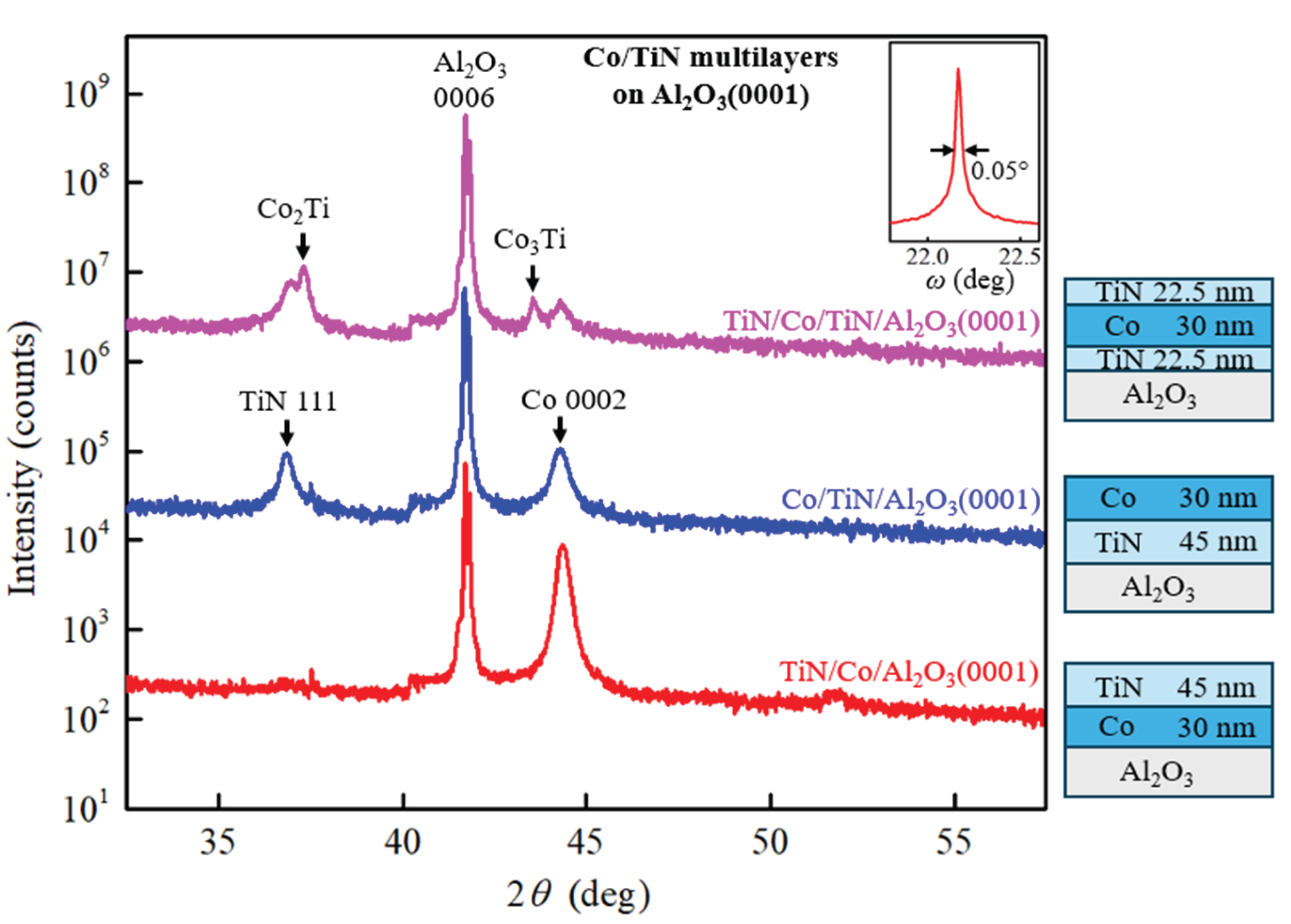
Figure 1. X-ray reflectivity curves from 50-nm-thick Co/TiN multi-layer films containing N = 1 – 10 Co layers. The dotted line is the result from curve fitting for N = 2.
Preprints 181679 g001
Figure 2. Grazing incident X-ray diffraction patterns from 50-nm-thick Co/TiN multilayer films with N = 1 – 10 Co layers. The inset shows the 0002 peak widths of 0.70° and 0.73° from the N = 1 and N = 10 samples, respectively.
Preprints 181679 g002
Figure 3. Resistivity ρ vs individual Co layer thickness dCo in 50-nm-thick Co/TiN multilayer films measured at 77 and 293 K. The solid lines are results from curve fitting using Eq. (1).
Preprints 181679 g003
Figure 4. XRD θ-2θ patterns from 75-nm-thick Co/TiN bilayer and trilayer stacks deposited on Al2O3(0001) at 600 °C. The inset shows the ω rocking of the Co 0002 peak for TiN/Co/ Al2O3(0001).
Preprints 181679 g004
Table 1. Sheet resistance Rs from Ti/Co layers deposited on Al2O3(0001).
Rs (Ω/sq)
TiN / Co / Al2O3(0001) 4.7
45 nm 30 nm
Co / TiN / Al2O3(0001) 8.0
30 nm 45 nm
TiN / Co / TiN / Al2O3(0001) 18.1
22.5 nm 30 nm 22.5 nm
TiN / Al2O3(0001) 23.8
45 nm
Co / Al2O3(0001) 3.3
30 nm
Disclaimer/Publisher’s Note: The statements, opinions and data contained in all publications are solely those of the individual author(s) and contributor(s) and not of MDPI and/or the editor(s). MDPI and/or the editor(s) disclaim responsibility for any injury to people or property resulting from any ideas, methods, instructions or products referred to in the content.
Copyright: This open access article is published under a Creative Commons CC BY 4.0 license, which permit the free download, distribution, and reuse, provided that the author and preprint are cited in any reuse.
Prerpints.org logo

Preprints.org is a free preprint server supported by MDPI in Basel, Switzerland.

Subscribe

Disclaimer

Terms of Use

Privacy Policy

Privacy Settings

© 2026 MDPI (Basel, Switzerland) unless otherwise stated