
Submitted:
09 October 2025
Posted:
10 October 2025
You are already at the latest version
Abstract
Absorption spectra are widely used in laboratory practice to measure the content of a great vari-ety of colloidal semiconductor nanocrystals. In the case of atomically thin nanoplatelets, only CdSe has been studied enough to allow such quantification, while CdTe nanoplatelets – a prom-ising material for photodetection – are understudied in this regard.
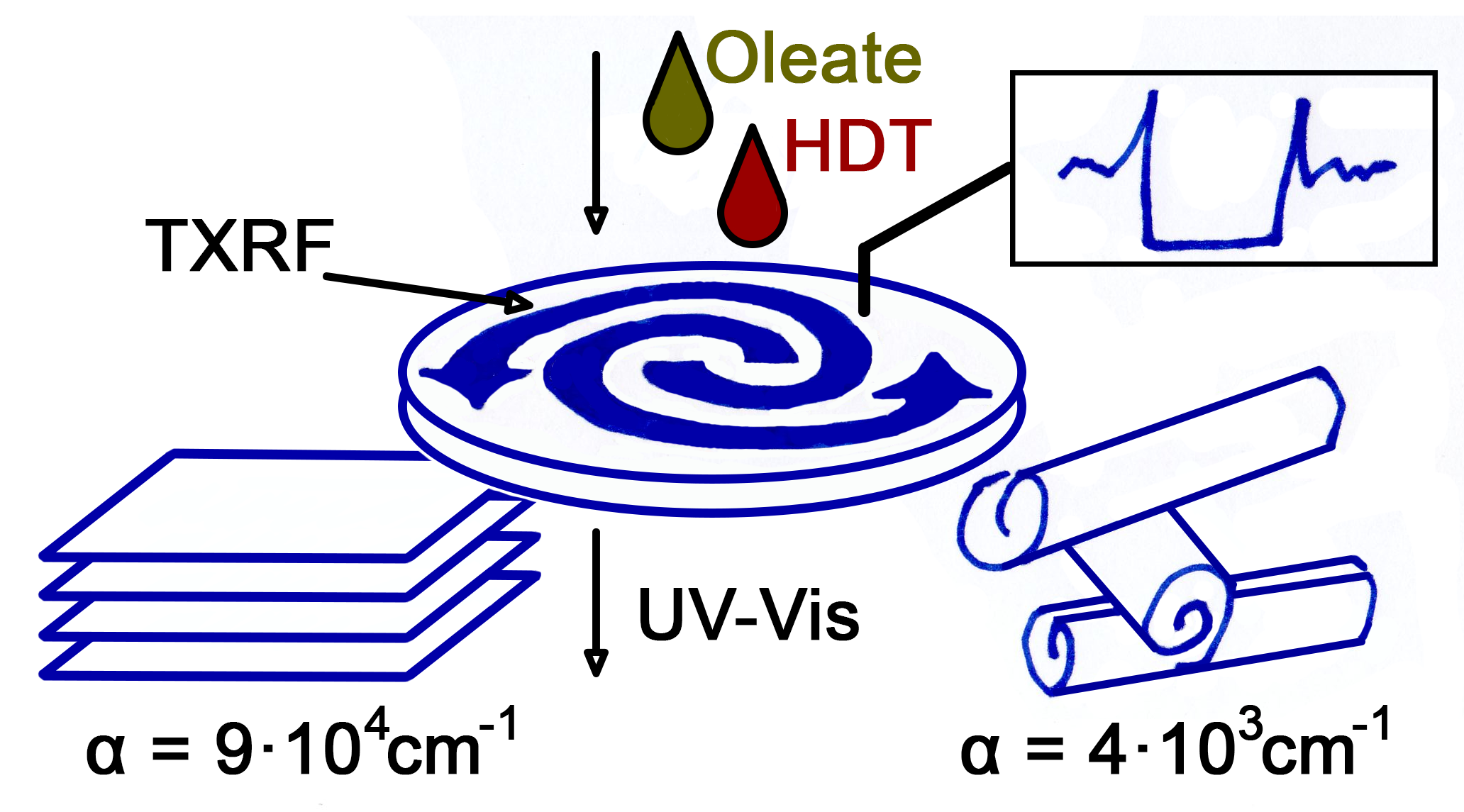
In this work, a powerful combination of total XRF spectroscopy, absorption spectroscopy and profilometry were employed for thin films to extract the absorption coefficient values. The morphology and surface composition of nanoplatelets were studied with TEM and IR spectros-copy.
Molar absorption coefficient of oleate-terminated CdTe nanoplatelets at the first optical transi-tion was measured at about 5·104 M-1·cm-1 (per mole of Te), which is among the highest values for AIIBVI nanomaterials. Exchange of stabilizer to hexadecanethiol induced approximately a 5-fold decrease in the volume fraction of semiconductor material in thin films and a 5-fold decrease in absorbance.
The latter effect is linked to the formation of quasi-type II heterojunction between CdTe cores and effectively a half of a monolayer shell of CdS. The density effect is explained with diminished capacity of nanoscrolls for close packing. The combination of XRF and profilometry is proposed as a technique for fast nanomorphology evaluation.
Keywords:
nanoplatelets
; CdTe
; absorption coefficient
; ligand exchange
; total X-ray fluorescence
1. Introduction
Semiconductor nanomaterials have been extensively researched for the past decades. In large part this is due to their robust and often tunable optical properties. The focal point of this attention has gradually shifted from colloidal AIIBVI quantum dots [1] to the largely lead-based perovskite systems [2], and then to the more sophisticated materials like nanoplatelets (NPLs) [3] and colloidal quantum shells [4]. The same optical properties are frequently used as a readily available and quick probe of the mean size of an ensemble, polydispersity [5] or concentration of nanoparticles. It is not surprising then, that the seminal work of Peng et al. on calibration curves for cadmium chalcogenide quantum dots [6] has accumulated more than 6 thousand citations to date.
Nanoplatelets are flexible 2D nanostructures, that are essentially monodisperse in their thickness of just several atomic layers, but can be grown to hundreds of nanometers in their lateral dimensions [7,8,9]. Their inorganic cores are almost entirely "surface" in the sense the whole lattice is distorted and a lowered crystal symmetry can be observed in diffraction patterns [9]. Of course, in these conditions the surface capping agent plays an integral role in formation and stabilization of the material and can even impart its own properties, like optical rotation, on the inorganic core [9]. NPLs are also sought for due to their uniquely narrow absorption and photoluminescence features [10] and giant oscillator strengths at low temperatures [11], high exciton binding energy [12], picosecond radiative recombination and high efficiency [13].
Unexpectedly, the literature corpus on absorption coefficients of atomically-thin NPLs consists of only a few well-executed studies. CdSe is, yet again, the more studied system: the spectral dependencies were reported not only on the principal parameter of NPL thickness [14,15,16,17], but also on the lateral size, on which an unusual non-quadratic scaling was observed [14]. The same set of publications also contains theoretical insight into absorption coefficients. As for CdTe NPLs, there is a single work [18] on these objects wherein UV-Vis spectroscopy was combined with optical profilometry to obtain an absorption coefficient α of 1.5·104 cm-1 for thin films.
The elemental composition and narrow band gap (1.44 eV) of CdTe make NPLs of this compound one of the most promising materials for photovoltaics, photodetection and radiation detection [19]. The flat two-dimensional shape of CdTe nanosheets enhances their technological compatibility with flexible substrates and typical microfabrication methods, expanding the possibilities of use in flexible electronic and optoelectronic systems. In our work we would like to build upon the existing work on the optical response of CdTe NPL films with addition of another powerful characterization technique – TXRF spectroscopy. In a “bottom-up” approach to our deductions, we aim to explore the relations between the nature of passivating ligand, nanomorphology and light attenuation in a NPL film.
2. Materials and Methods
2.1. Chemicals
The chemicals used were 1-octadecene (ODE) (Sigma-Aldrich, 90%), propionic acid (Sigma-Aldrich, 99%), oleic acid (OA) (Sigma-Aldrich, 90%), cadmium acetate dihydrate (Cd(OAc)2·2H2O) (>98%), tellurium powder (Te) (98%), hexadecanthiol (Aldrich, >95%), oleylamine (Aldrich, 70%), trioctylphosphine (Aldrich, 95%), hexane (>99%), ethanol (95%), acetone (>99%) dichloromethane (CH2Cl2) (>99%).
2.2. Precursor Preparation
Cadmium propionate Cd(Prop)2: to prepare the cadmium propionate precursor, 8.07 mmol (2.15 g) of cadmium acetate dihydrate and 10 mL (133 mmol) of propionic acid were mixed in a 50 mL three-neck flask and stirred at 90 °C under argon for one hour. After one hour, the mixture was cooled to approximately 50-60°C and acetone was introduced until the solution turned turbid. White precipitate of cadmium propionate was filtered and dried.
Trioctyolphosphine telluride: to prepare the tellurium precursor 1 mmol (0.1276 g) of tellurium powder was added to 1 ml of trioctylphosphine. The powder was dispersed in ultrasonic bath until full tellurium powder dissolution.
2.3. Synthesis of CdTe NPLs
In present work we utilized the synthetic technique proposed by Pedetti et al. [18] with our minor modification described in [20]. Briefly, for typical synthesis of CdTe NPLs 0.5 mmol (130 mg) of cadmium propionate, 0.25 mmol (80 μL) of oleic acid and 10 mL of 1-octadecene were added into 50 mL three-neck flask. The mixture was heated under argon to 110 °C with stirring and degassed for 30 min. After that the temperature was raised to 170 °C and 100 μL of 1 M trioctylphosphine telluride solution diluted by 0.5 mL of ODE was injected. Upon injection, the color changes to dark yellow and then to orange. After 20 min of NPLs growth 1 mL of OA was injected and the mixture was cooled to room temperature. The product was isolated by addition the excess of acetone (1:2 by volume) with subsequent centrifugation at 8000 rpm for 5 min and redispersion in hexane.
2.4. Ligand Exchange
2 mL (4.2 μmol in cadmium) of raw CdTe NPLs sample was mixed with 8 mL of hexane and 800 μL of hexadecanethiol and stirred under argon for 30 min for degassing. After 30 min the temperature was raised to 65°C and 150 μL of oleylamine was injected and the mixture was stirred for 1 h. Upon cooling to room temperature, the sol color maintained yellow, while successful ligand exchange should result in red or dark-red color [7]. The mixture was left for 2 days to complete exchange reaction what resulted in red coloration. Equal volume of acetone was introduced to precipitate the NPLs from the reaction mass. The product was centrifuged at 18000 rpm for 2 min and redispersed in hexane.
2.5. Spin-Coating Technique
In order to deposit uniform films, the initial CdTe NPLs sample was redispersed in CH2Cl2 with the same protocol as the one described in the Section 2.4. 1 mL of raw CdTe NPLs sample was sedimented, centrifuged and dispersed in 1.5 mL of dichloromethane. Thiol-exchanged CdTe NPLs sample dispersed in CH2Cl2 gave non-uniform films so we used initial hexane-based sols. The films were formed by deposition of 700 μL of sols onto monocrystalline sapphire substrates. Different films of the same NPL sample were deposited for profilometry and for TXRF studies.
2.6. Characterization and Equipment
The UV–Vis absorption spectra were recorded on Varian Cary 50 spectrometer against a clean sapphire substrate used as a baseline. IR spectra were taken on PerkinElmer Frontier FTIR spectrometer with Pike diffusion reflection module. For the sake of this measurements, NPL sols were drop-cast on gold mirrors and dried.
Transmission electron microscopy (TEM) studies were conducted using a JEOL JEM-2100 microscope equipped with a LaB6 gun and an 11-megapixel Olympus Quemesa CCD camera. The accelerating voltage was set to 200 kV. Hexane sols containing NPLs were deposited onto carbon-coated copper grids and dried. The grids were then etched in argon plasma to remove organic material before examination. The sizes of the NPLs were measured from micrographs using Image-Pro Plus 6.0 software.
Composition analysis was conducted using X-ray Fluorescence (XRF) Bruker M1 Mistral spectrometer (tungsten anode) and a Total X-ray Fluorescence (TXRF) Bruker Picofox S2 spectrometer (MoKα radiation). In the case of XRF measurements the spectra were collected for 15 minutes. Several spectra were taken in different parts of the film with 2 mm radius of the film’s center. Constant intensity of the oncoming radiation was confirmed by recording the XRF spectra of silver substrate prior to and after the measurements. In the case of TXRF studies, the outer regions of the spin-coat deposited film were removed until a roughly 3 mm in diameter spot was left in the center of the substrate. The beam width in the instrument is 1 cm.
The thickness of the films was determined with use of a Taylor-Hobbson TalyStep profilometer. The films themselves are too soft to allow step-profilometry, so after the grooves were made in the film, a thick (~0.5 μm) copper layer was deposited on top of it in a vacuum chamber of VUP-5 apparatus by thermal evaporation.
3. Results and Discussion
We start our discussion by examining the dimensions and morphology of the studied particles. Determination of NPL thickness is a cumbersome task, however, it can be circumvented by the fact that it stays constant within a certain NPL population. The population itself is uniquely characterized by the position of its first absorption maximum. In our case, the position at 500 nm corresponds to 3.5 monolayer 1.9±0.3 nm thick CdTe nanoplatelets [18]. The lateral dimensions of unexchanged NPLs were obtained with TEM imaging (Figure 1(a)). The fabricated NPL gravitate towards predominantly rectangular shape, often with splayed angles. Their mean lateral dimensions are 110×70 nm2, the distributions of lengths, widths and basal plane areas are given in Section S1 of the Supplementary Information. Exchange of stabilizer with thiol, expectedly [7], leads to formation of nanoscrolls with mean radius of curvature of 9 nm (Figure 1(b)).
Ligand exchange is confirmed by IR spectra as well (Figure 2). After thiol treatment almost the entirety of the spectrum is explained with C-H vibrations: functional group region only reveals characteristic C-H bands: νas(CH3) at 2955 cm-1, νas(CH2) at 2920 cm-1, νs(CH2) at 2850 cm-1, scissoring vibration of CH2 at 1470 cm-1, rocking vibration of CH2 at 720 cm-1 [21]. At the same time, the contribution of carboxylate vibrations is greatly diminished: only the strongest band of νas can be seen at 1530 cm-1. The spectrum of the original NPLs is richer in features. For instance, ν(=C-H) is seen at 3010 cm-1 and (COO-) – at 1410 cm-1 [9,21].
Next, we explore the properties of NPLs in the form of thin films. For these objects the question of thickness is of utmost importance. In this work we assessed the thickness with two methods: step-profilometry and XRF. Profilometry allows to study thickness at a granular level, assess the film's surface roughness, measure absolute thickness values. Surface roughness was characterized with Ra parameter, the values of which were found for individual profiles and then averaged. The individual profile measurements for the film of thiol-covered NPLs were within 110 – 125 nm range and worked out to Ra of 120 nm. We averaged the thickness values within each profile and treated the result as a single measurement for the sake of statistics. The results are present in Table 1. The average thickness of this film is 590±60 nm. The uniformity is about ±15% of this value within 2 mm radius of the film’s center – a region, from which TXRF and UV/Vis absorption data were collected and where the thickness was studied. The relative value of roughness of the film of thiolated NPLs amounts to 20%. For a film of carboxylated NPLs we likewise obtain Ra of 20 nm and a mean thickness of 127±11 nm. The film is significantly thinner, but the quality in terms of relative parameters is similar to the thiolated case.
The thickness can also be evaluated via XRF, which serves as a complementary technique. When the thickness of the film is low, so that attenuation of outgoing characteristic X-rays is less than 5%, the intensity of characteristic fluorescence is proportionate to the areal density of an element. If we assume consistent density within one film and between different films of the same material and deposition conditions, then XRF intensity is proportionate to the film's thickness. As tungsten anode bremsstrahlung maximum lies at lower energy than TeKα, we only computed the intensity of the CdKα line. We did so by integration in the spectral region of 22.96 – 23.36 keV after the background was fit locally with a straight line. The choice of integration window is to minimize the error (Section S2 of the Supplementary Information). XRF measurements corroborate the profilometry results on film uniformity, the size of signal acquisition area does not allow to obtain roughness. We note here, that the precision of XRF as a thickness probe was comparable or better than that of step-profilometry, however, XRF thickness is in arbitrary units, so the final calculation would include the error of a direct method as well.
As UV-Vis absorption spectroscopy is a non-destructive method, it was possible to study the same films prior to profilometry. Absorbance values can then be normalized by the thickness to produce the spectral dependencies of the absorption coefficient α (Figure 3).
(black line) and thiol-exchanged (red line) NPLs.
A film made up of carboxylated NPLs attenuates light much more efficiently per unit length of optical path. In the region of 400 – 600 nm, where the respective first (electron – heavy hole) excitonic maxima of absorption are situated, the difference amounts to 1.5 orders of magnitude. Specifically, α500 for carboxylated NPLs is measured to be 94700 cm-1, while α523 for the thiolated sample is 3840 cm-1. These can be immediately compared to the previously measured value of 1.5·104 cm-1 for the films of the same carboxylated CdTe NPLs [18] and (2 – 3)·104 cm-1 measured for different populations of CdSe NPLs [15]. The observed differences between all these values are likely due to different efficiency of packing, as the films in Ref.18 were obtained with drop-casting. For a crystalline CdTe slab, the absorption coefficient is around 104-105 cm-1 across the visible part of the spectrum [22]: the band edge is immediately in its vicinity in the IR region for this direct narrow-band semiconductor. Transition into ultradisperse state blue-shifts the band gap and increases the oscillator strength of HOMO-LUMO transition because of quantum confinement [23]. Taking all these considerations into account, our observations are consistent with dilute films of CdTe NPLs.
Absorption coefficient α is the product of molar absorption coefficient ε and concentration, which is directly proportional to density of the film with respect to the light-absorbing material. To decouple the contribution of these factors to the observed difference between carboxylated and thiolated NPL films, we have studied another set of films with TXRF and absorption spectroscopy.
So long as the film is infinitesimally thin for the characteristic fluorescence, absolute masses of the elements are determined within the signal acquisition spot. These can be normalized for the area of the film to obtain areal density. When the latter parameter is divided over the molar mass, we obtain the c·l product of the Beer-Lambert’s law. Selected parameters from TXRF studies as presented in Table 2. We have used the values of areal density to confirm the correctness of the analysis. Mass attenuation coefficients μ for CdLα, TeLα and SKα [24] were divided by cos(30º), which is the mean angle between the normal to the sample and the detector of our instrument, as discussed in another our work, which currently under consideration [25]. The attenuation by organic matter was introduced as an additional term to μCd values, seen as organic stabilizers are bound to surface cadmium atoms. For the sake of this calculation, we estimated that 1 stabilizer moiety is present in the samples for every 2 Cd atoms (Cd4Te3X2 formula unit, where X is the organic stabilizer).
Even when multiplied by an angle-based factor, all μ values are below 1800 cm2/g (Section S3 of the Supplementary Information). From summation over the products ρA·μ we obtain that every line in question would be attenuated by less than 1% even by the full thickness of the film. Mean attenuation is then less than 0.5%, which is lower than the uncertainly in area determination, so no correction for the sample self-absorption was adopted. The Cd-to-Te ratio has changed dramatically after the ligand exchange procedure. While there are no apparent indications of this process in TEM images, we suggest that some of the NPLs could be etched with the excess of hexadecanethiol. The resultant cadmium thiolate is soluble in non-polar organics, is not colored, and therefore could remain unnoticed in the sample. Tellurides, on the other hand, are readily oxidized to the elemental form, which is insoluble and produces very apparent changes in the color of the sample. Due to that, we link the quantity of NPLs with Te content and normalize for it. Chalcogenide content has been used previously when there was a similar ambiguity in ε determination [14].
A factor of 4.63±0.15 difference remains between the molar absorption coefficients. It follows that there is 5-fold change in the volume fraction of CdTe cores fraction between the films of carboxylated and thiolated NPLs. This, of course, was indicated earlier by the XRF signal values for the first set of films (Table 1). We quantify the volume fraction by calculating concentration with the use of both α and ε values for the two sets of films, as well as density of bulk CdTe of 5.85 g/cm3. Films of carboxylated CdTe exhibit a volume fraction of inorganic cores of 8%, thiolated films - 1.5%. The densest possible packing occurs through stacking of NPLs and interdigitation of organic terminating chains. In a stack on NPLs the volume fraction of cores can be assessed by relating the core thickness to the stacking period, measured with TEM. For the 500 nm population of alkylated CdTe NPLs an estimate of 30 – 40% can be obtained from the literature [18].
The difference in packing density appears feasible. Pre-formed scrolls are incapable of stacking in the same manner as flat NPLs. The folding is spontaneous and therefore should reach only local energy maxima. Inherent (comparatively) poor control over lateral dimensions of NPLs [26,27] leads to scrolls that are mismatched in their form, working further to slightly detriment the density of closest attainable packing. Moreover, there is a "dead volume" inside of the scroll, which is unable to accommodate other NPL cores. We advocate for the combination of (T)XRF spectroscopy and profilometry of thin films as a fast and high-throughput technique to evaluate or control NPL morphology. We have to note that XRF intensity is very well correlated to absorbance when we compare different films of the same material (Table 1 and Table 2, Figure 3).
When the difference in packing is accounted for, the difference in the intensity of optical response between NPLs with different anchor groups of ligands remains very substantial. Quantitative models for a quantum well always include direct proportionality between the absorption cross-section and frequency [14,16,18], however, between 500 and 523 nm there is only a factor of 1.05 difference. Next, we evaluate surface and dielectric effects. A particular study [28] has shown that the per-mole-value of ε for ZnSe colloidal quantum dots grows sharply with decreasing nanocrystal diameter, already reaching 104 M-1·cm-1 at the first maximum frequency for the mean diameter of 4 nm. This can be rationalized either with the effect of quantum confinement on the electron-hole pair, or with better electromagnetic field penetration of the cores [16]. Both these effects work to the advantage of NPLs in terms of the magnitude of ε [16,17], moreover, in the case of CdTe both elements are the heavier counterparts to the components of ZnSe, and have higher polarizability that is beneficial for light-matter interactions. The value of ε was measured at 2·104 M-1·cm-1 for 513 nm population of CdSe NPLs [14], which is in line with our findings and deductions. We note here, that the absorption efficiency is also frequently presented as intrinsic absorption coefficient, we calculate this value for oleate-capped CdTe NPLs to be 2.8·106 cm-1 at the first exciton transition, even higher than that of 2 monolayer CdSe NPLs [17]. In the search for the ultimate light-absorbing material an investigation of thinner CdTe NPL populations is warranted.
The role of surface states was highlighted in the case of ZnSe quantum dots. Se-terminated cores have shown the values of ε at the first maximum of transition almost 2 times higher than that of their Cd-terminated counterparts [28]. In our case, what is essentially an addition of a layer of sulfur on the surface of NPLs lowers the molar absorption coefficient by about a factor of 5. To explain that we recall that in bulk the conduction band alignment of CdTe and CdS is rather close [29], and that strain can shift band energy in nanostructures to result in quasi-type II heterojunctions [30,31]. We believe that sulfur atoms in thiolated CdTe NPLs provide surface states for electrons thus decreasing the wavefunction overlap with holes.
4. Conclusions
We have constructed a robust protocol for determination of absorption coefficients of NPLs through addition of X-ray fluorescence spectroscopy to the existing group of characterization methods. Thin film form ensures homogeneity and effectively combats the ever-present problem of NPL sedimentation and absorption on cuvette surfaces during the handling of sols. At the same time, minimal sample preparation required for the XRF studies eliminates possible associated systematic errors.
The molar absorption coefficient at the first optical transition of CdTe NPLs is measured at a significantly higher value (4.95±0.12)·104 M-1 cm-1 (per mole of Te) than in prior works, further proving the capacity of CdTe for light detection. When carboxylate stabilization is exchanged for thiolate this value drops to (1.07±0.03)·104 M-1 cm-1. This is additional evidence for formation of quasi-type II structure between CdTe cores and Cd thiolate capping layer.
Scroll-like morphology, attained through ligand exchange, translates to 5 times lower volume fraction of inorganic cores in the films fabricated by spin-coating. A combination of profilometry and XRF spectroscopy can then be employed to infer NPL morphology without TEM studies.
Supplementary Materials
The following supporting information can be downloaded at the website of this paper posted on Preprints.org, Figure S1: Histograms of linear dimensions of nanoplatelets under study, Figure S2: Relative error in CdKα line areal intensity determination as a function of integration interval, data for carboxylated NPLs film prepared for TXRF studies is used as an example, Table S3: Mass attenuation coefficients for self- and cross-absorption of nanoplatelet constituent elements.
Author Contributions
Conceptualization S.D.; Funding acquisition A.K.; Investigation S.B., A.O., S.D., K.C., A.A. and D.D.; Methodology S.D. and D.D.; Project administration D.D.; Resources A.K. and D.D.; Supervision S.D. and A.K.; Validation А.V.; Visualization A.O.; Writing – Original draft preparation S.B., A.O. and A.V.; Writing – Review and editing A.V. All authors have read and agreed to the published version of the manuscript.
Funding
The part of this research performed by the group from ENU (material and film fabrication, optical measurements, profilometry) was funded by the Science Committee of the Ministry of Science and Higher Education of the Republic of Kazakhstan (Grant №. AP19676416). The work of the group from MSU (XRF and IR spectroscopy) was supported through the Lomonosov Moscow State University Program of the Development within state contract АААА-А21-121011590082-2.
Data Availability Statement
The original contributions presented in the study are included in the article/supplementary material; further inquiries can be directed to the corresponding author/s
Acknowledgments
The authors acknowledge support from M. V. Lomonosov Moscow State University Program of Development in the form of access to a Frontier FTIR spectrometer and an S2 Picofox TXRF spectrometer.
Conflicts of Interest
The authors declare no conflicts of interest
References
- García de Arquer F. P. et al. Semiconductor quantum dots: Technological progress and future challenges // Science. – 2021. – V. 373. – № 6555. [CrossRef]
- Katan C. et al. Quantum and dielectric confinement effects in lower-dimensional hybrid perovskite semiconductors // Chemical reviews. – 2019. – V. 119. – №. 5. – P. 3140-3192. [CrossRef]
- Singh S. et al. Colloidal CdSe nanoplatelets, a model for surface chemistry/optoelectronic property relations in semiconductor nanocrystals //Journal of the American Chemical Society. – 2018. – V. 140. – №. 41. – P. 13292-13300. [CrossRef]
- Cassidy J. et al. Colloidal quantum shells: an emerging 2D semiconductor for energy applications //ACS Energy Letters. – 2022. – V. 7. – №. 3. – P. 1202-1213. [CrossRef]
- Park J. et al. Nanocrystal Precursor Incorporating Separated Reaction Mechanisms for Nucleation and Growth to Unleash the Potential of Heat-up Synthesis // ACS Nano. – 2020. – V. 14. – P. 11579-11593. [CrossRef]
- Yu W. W. et al. Experimental determination of the extinction coefficient of CdTe, CdSe, and CdS nanocrystals //Chemistry of materials. – 2003. – V. 15. – №. 14. – P. 2854-2860. [CrossRef]
- Vasiliev R. B. et al. Spontaneous folding of CdTe nanosheets induced by ligand exchange //Chemistry of materials. – 2018. – V. 30. – №. 5. – P. 1710-1717. [CrossRef]
- Bouet C. et al. Two-Dimensional Growth of CdSe Nanocrystals, from Nanoplatelets to Nanosheets // Chemistry of Materials. – 2013. – V. 25. - № 4. – P. 639-645. [CrossRef]
- Kurtina D. A. et al. Atomically Thin Population of Colloidal CdSe Nanoplatelets: Growth of Rolled-up Nanosheets and Strong Circular Dichroism Induced by Ligand Exchange // Chemistry of Materials. – 2019. – V. 31. - № 23. – P. 9652-9663. [CrossRef]
- Joo J. et al. Low-Temperature Solution-Phase Synthesis of Quantum Well Structured CdSe Nanoribbons // Journal of the American Chemical Society. – 2006. – V. 128. - № 17. – P. 5632–5633. [CrossRef]
- Diroll B.T. et al. Reexamination of the Giant Oscillator Strength Effect in CdSe Nanoplatelets // J. Phys. Chem. C 2023, 127, 9, 4601–4608. [CrossRef]
- Scott, R. et al. Time-Resolved Stark Spectroscopy in CdSe Nanoplatelets: Exciton Binding Energy, Polarizability, and Field-Dependent Radiative Rates // Nano Letters. – 2016. – V. 16 – № 10 – P. 6576– 6583. [CrossRef]
- Tessier M. D. et al. Spectroscopy of Single CdSe Nanoplatelets // ACS Nano. – 2012. – V. 6 – № 8. – P. 6751–6758. [CrossRef]
- Yeltik A. et al. Experimental Determination of the Absorption Cross-Section and Molar Extinction Coefficient of Colloidal CdSe Nanoplatelets // Journal of Physical Chemistry C. – 2015. – V. 119. – P. 26768-26775. [CrossRef]
- Zhang Z. et al. Study of Complex Optical Constants of Neat Cadmium Selenide Nanoplatelets Thin Films by Spectroscopic Ellipsometry // Journal of Physical Chemistry Letters. – 2021. – V. 12. – P. 191-198. [CrossRef]
- Achtstein A. W. et al. Linear Absorption in CdSe Nanoplates: Thickness and Lateral Size Dependency of the Intrinsic Absorption // Journal of Physical Chemistry C. – 2015. – V. 119. – P. 20156-20161. [CrossRef]
- Delikanli S. et al. Ultrathin Highly Luminescent Two-Monolayer Colloidal CdSe Nanoplatelets // Advanced Functional Materials. – 2019. – V. 19. – 1901028. [CrossRef]
- Pedetti S. et al. Optimized synthesis of CdTe nanoplatelets and photoresponse of CdTe nanoplatelets films // Chemistry of Materials. – 2013. – V. 25. – №. 12. – P. 2455-2462. [CrossRef]
- Anand A. et al. Optical and scintillation properties of record-efficiency CdTe nanoplatelets toward radiation detection applications // Nano Letters. – 2022. – V. 22. – №. 22. – P. 8900-8907. [CrossRef]
- Ospanova A. et al. Investigation of the influence of structure, stoichiometry, and synthesis temperature on the optical properties of CdTe nanoplatelets //Nanomaterials. – 2024. – V. 14. – №. 22. – P. 1814. [CrossRef]
- Tarasevich BN (2012) IR Spectra of Main Classes of Organic Compounds. Moscow State University, Moscow.
- Mitchell K et al. Photovoltaic determination of optical-absorption coefficient in CdTe // Journal of Applied Physics. – 1977. – V. 48. - № 2. – P. 829-830. [CrossRef]
- Moreels I. et al. Size-dependent optical properties of colloidal PbS quantum dots // ACS Nano. – 2009. – V. 3. – № 10. – P. 3023-3030. [CrossRef]
- Blokhin MA, Shweitzer IG (1982) Rentgenospectral handbook. Nauka, Moscow.
- Bubenov et al. Depth profiling of phosphorus impurity in silicon nanocrystals by X-ray fluorescence and IR region localized surface plasmon resonance // Silicon. – 2025. (Submitted).
- AL-Shnani et al. Fluorescence Quantum Efficiency Enhancement in Size-Controlled 3.5 Monolayer Cadmium Telluride Nanoplatelets // Chemistry of Materials. – 2023. – V. 35. - № 16. – P. 6258-6265. [CrossRef]
- Yu J. et al. Effect of Lateral Size and Surface Passivation on the Near-Band-Edge Excitonic Emission from Quasi-Two-Dimensional CdSe Nanoplatelets // ACS Appl. Mater. Interfaces. – 2019. – V. 11 – № 44. – P. 41821–41827. [CrossRef]
- Lin S. et al. Surface and intrinsic contributions to extinction properties of ZnSe quantum dots // Nano Research. – 2020. – V. 13. – № 3 – P. 824-831. [CrossRef]
- Reiss P. et al. Core/Shell Semiconductor Nanocrystals // Small. – 2009. – V. 5. – № 2. – P. 154-168.
- Smith A.M. et al. Tuning the optical and electronic properties of colloidal nanocrystals by lattice strain // Nature Nanotechnology. – 2009. – V. 4. – P. 56-63. [CrossRef]
- Lin S. et al. Nucleation and Growth of Monodisperse CdTe and CdTe/ZnSe Core/shell Nanocrystals: Roles of Cationic Precursors, Ligands, and Solvents // Journal of the American Chemical Society. – 2025. – V. 147. – P. 12962-12972. [CrossRef]
Figure 1.
TEM images of: a) initial sample; b) thiol-treated sample.
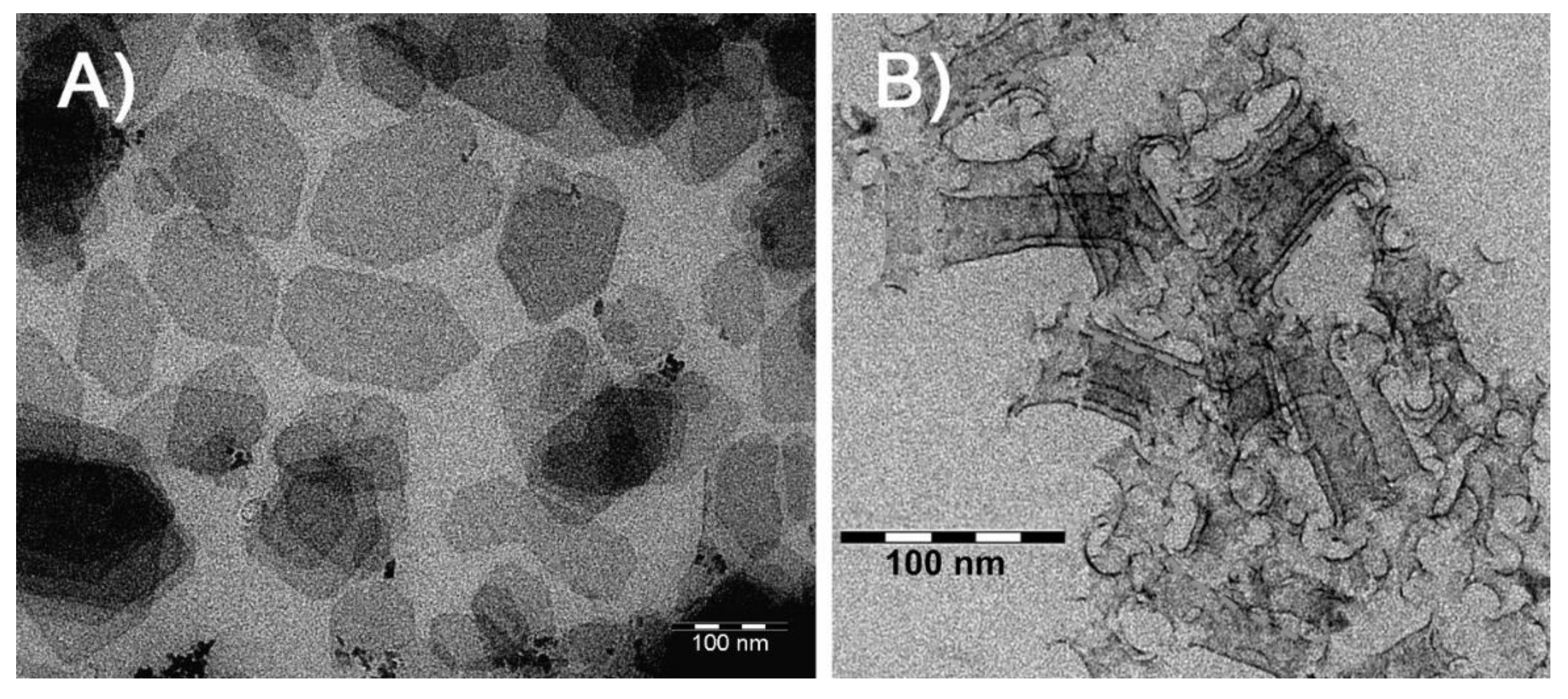
Figure 2.
IR spectra of NPLs sample prior to thiol treatment (black line) and after thiol treatment (red line). The spectra are normalized for the intensity of valent C-H vibrations and offset vertically for clarity. The transmittance in the experiments was no less than 30% in the entirety of the spectrum, so the line shapes are not distorted. The break region in the plot is featureless.
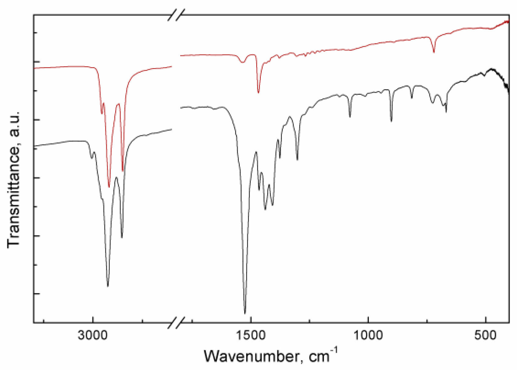
Figure 3.
Spectral dependencies of absorption coefficients of films of carboxyl-terminated.
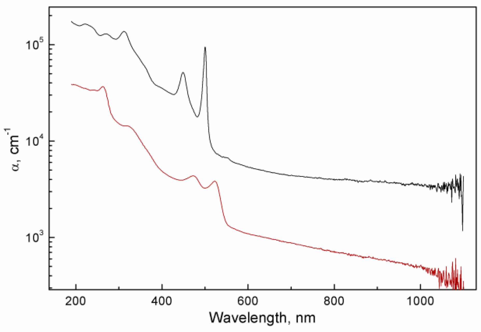

Table 1.
Thickness and XRF intensity for films of CdTe NPLs.
| Sample | carboxylated NPLs | thiolated NPLs |
|---|---|---|
| Thickness, nm | 113±10 | 510±70 |
| 119±15 | 520±140 | |
| 120±40 134±18 135±18 142±15 |
570±80 610±60 640±130 690±70 |
|
| CdKα line intensity, a.u. | 240±30 | 200±20 |
| 230±30 | 190±20 | |
| 220±30 | 190±20 190±20 200±20 |
Table 2.
Collated data on molar extinction coefficient determination for CdTe NPLs.
| Sample | Carboxylated_2nd | Thiolated_2nd | |
|---|---|---|---|
| S, cm2 | 0.0802±0.0018 | 0.132±0.003 | |
| m, ng | Cd | 465±3 | 626±3 |
| Te | 474±3 | 404±3 | |
| S | 1.7±0.9 | 279±3 | |
| Areal density, μg/cm2 |
Cd | 4.46±0.11 | 4.75±0.11 |
| Te | 4.95±0.12 | 3.06±0.07 | |
| S | <0.04 | 2.12±0.05 | |
| Stoichiometry parameter, nCd/nTe | 1.02 | 1.76 | |
| XRF intensity, a.u. | 360±30 | 190±20 | |
| 370±30 | 190±20 | ||
| 370±30 | 190±30 | ||
| 372±17 | 200±30 | ||
| 210±20 | |||
| Absorbance (wavelength, nm) | 1.92 (500) | 0.258 (523) | |
| ε(per mole of Te), M-1·cm-1 | (4.95±0.12)·104 | (1.07±0.03)·104 | |
Disclaimer/Publisher’s Note: The statements, opinions and data contained in all publications are solely those of the individual author(s) and contributor(s) and not of MDPI and/or the editor(s). MDPI and/or the editor(s) disclaim responsibility for any injury to people or property resulting from any ideas, methods, instructions or products referred to in the content. |
© 2025 by the authors. Licensee MDPI, Basel, Switzerland. This article is an open access article distributed under the terms and conditions of the Creative Commons Attribution (CC BY) license (http://creativecommons.org/licenses/by/4.0/).
Copyright: This open access article is published under a Creative Commons CC BY 4.0 license, which permit the free download, distribution, and reuse, provided that the author and preprint are cited in any reuse.


