
Submitted:
03 October 2025
Posted:
07 October 2025
You are already at the latest version
Abstract
Correlation-Assisted Direct Time-of-Flight (CA-dToF) is demonstrated for the first time with a 320×240-pixel SPAD array. SPAD triggers are processed in-pixel, avoiding data communication over the array and/or storage bottlenecks. This is accomplished by sampling two orthogonal triangle waves that are synchronized with short light pulses illuminating the scene. Using small switched-capacitor circuits, exponential-moving-averaging (EMA) is applied to the sampled voltages, delivering two analog voltages (VQ2, VI2). These contain the phase delay, or the time of flight between the light pulse and photon’s time of arrival (ToA). Uncorrelated ambient photons and dark counts are averaged out, leaving only their associated shot noise impacting the phase precision. The QVGA camera allows capturing depth-sense images with sub-cm precision over 6-m range of detection, even with a small PDE of 0.7% at 850-nm wavelength.
Keywords:
3D-ToF
; CA-dToF
; LIDAR
; switched capacitors
; exponential moving average
; SPAD
; depth sensing
1. Introduction
Time-of-flight (ToF) imaging has emerged as a key technique for depth sensing, with growing attention due to its potential in applications requiring efficient power usage, high-resolution imaging, and accurate distance measurements with low uncertainty [1]. These performance demands are particularly relevant in areas such as automotive machine vision and portable consumer devices, including smartphones and laptops [2]. Among ToF approaches, the two dominant methods are direct time-of-flight (dToF) and indirect time-of-flight (iToF) [3,4,5].
In iToF, a modulated light source illuminates the scene in synchronization with a photonic mixer device shutter, and the time of flight is extracted from the phase shift between the emitted and reflected signals. In contrast, dToF measures photon arrival times directly, generating a histogram of detected events. This approach employs short-pulsed laser illumination and avalanche detectors, with arrival times digitized or converted into analog values [3]. Considerable research efforts have been devoted to evaluating the theoretical limits and practical performance of these methods, as well as to addressing the constraints imposed by their underlying device technologies.
Among these efforts is the recent development of a correlation-assisted direct time-of-flight pixel (CA-dToF), which was first presented based on sine and cosine demodulation using a single-stage exponential moving average (EMA) for measuring depth, using a 32×32 prototype array [6]. Furthermore, an analytical model was developed, and a 100 klux solar ambient light suppression was demonstrated [7]. The pixel showed reliable performance under challenging ambient light conditions and flexibility in performance and optimization. The systematic and environmental challenges of the pixel implementation showed a common challenge with iToF [4]. However, the CA-dToF pixel can tackle such challenges as presented in [8].
We now demonstrate the operation of a camera containing a QVGA 320×240-pixel image sensor whereby the pixels use a cascade of two averaging stages, increasing the in-pixel available averaging level (AA) to the product of the two. The first averaging stage samples at each SPAD trigger, the second stage is this time operated at a switching rate which is varied during each sub-frame, for quick convergence of the average voltages and optimal noise reduction.
If the number of incoming photon triggers within a subframe is less than the AA, we get unharmful over-averaging, assuming uniformly spread ambient (A) and reflected signal (S) photons. For this over-averaging situation, a comprehensive model will now provide an estimation of the depth’s standard deviation.
Further, in this work, we demonstrate the use of triangular signals (TSIN, TCOS) instead of sinusoidal signals, simplifying the analog driving circuit. An analog photon counter is also implemented for grey-image capture. The pixel has an area of 30×30 mm2, including SPAD (Ø = 10 m), delivering a small fill factor (8.7%) and hence low PDE (~0.7%) at l = 850 nm.
2. Used Subcircuits Based on Switched Capacitors
Three different circuits with common circuitry elements and operating principles are discussed first: two for averaging voltage samples and one for photon counting. The latter is included for acquiring a grey image with and without laser illumination of the scene, which is required to validate the provided depth precision model.
2.1. Exponential Moving Average and Its Implementation
When dealing with a noisy and continuous stream of measurements of a given quantity, predicting the underlying trend based on previous observations presents a significant challenge. A straightforward approach is the simple moving average (SMA), in which each predicted value is obtained by computing the mean of the most recent navg samples. Based on a Gaussian spread assumption, noise is reduced with . However, if the underlying trend is changing, one must compromise between accuracy and precision depending on the number of samples. Figure 1 shows this SMA, over 30 samples, updated after every incoming sample.
Another type of averaging is the exponential moving average (EMA). In this system one doesn’t need to memorize the list of the last navg samples, one only keeps the latest average itself. Every time a new sample enters, an update to this average is made by taking the new sample into account in a weighted way depending on an averaging number navg: this parameter also reflects (roughly) over how many samples averaging is performed.
These SMA and EMA averages are calculated as follows:
whereby represents every new incoming sample. Notice that the samples may arrive at irregular intervals. The average updates at the arrival of each new sample. Besides not needing to memorize a table of samples, the EMA has the property to weigh the importance of the past samples in a variable way; the longer ago a sample was taken, the less it weighs into the average. Depending on the application, this can be considered an advantage or a disadvantage. However, for image sensors the EMA-principle has the undeniable advantage that it only needs to memorize one value. Moreover, it can be implemented with the elementary circuit given in Figure 2.
From charge conservation (before and after short circuiting), we get the updated EMA as follows:
whereby Equation 3 is the same as equation 2 with the averaging number depending on the ratio of the two involved capacitors. These equations prove that this simple circuit can implement the EMA based on voltage domain signals.
The practical implementation in CMOS circuitry may use various types of capacitors and switches. CMOS switches (using both an NMOS and a PMOS transistor) as well as pass gates (based solely on an NMOS or PMOS transistor) are preferred due to their compact design when integrated in a pixel. We opted to use NMOS transistor pass gates, allowing the construction of a very low parasitic capacitance Cs. Figure 3 shows how such small Cs can be made: we use the parasitic drain/source between T1 and T2 to get the smallest achievable area depending on design rules. The capacitance is derived from the parasitic extract and is 0.251 fF. The connected PMOS gate capacitance is 49 fF. So navg is ~ 200 which is confirmed by spice simulations on the extracted circuits. The parasitic capacitance experiences some non-linearity, which should be considered for each target application. Cint can be made with a varactor, or with the gate of a PMOS transistor (shown in Figure 8). There is some variability in Cs when based on a parasitic node for its implementation due to process variation and statistical spread. Hence the implemented value for navg also varies. When used merely for averaging, this is of a lesser concern than when used for photon counting, where the gain of the counter becomes variable too.
The clocks (F1, F2) must not be high simultaneously to avoid shorting the two capacitors; this can easily be achieved with a few logic gates, e.g., two NOR gates and a NOT gate.
2.2. More Averaging: Use of Switched Capacitor Low-Pass Filter(s)
When one needs much larger averaging numbers, making just an extremely large Cint is not an option inside a small sensor pixel. Alternatively, a second averaging stage can be implemented based on a switched capacitor circuit using similar circuit topology. It is based on a textbook low-pass filter circuit:
Figure 4.
By periodically toggling the switch, a low-pass filter is constructed with -3dB corner frequency settable by the toggling frequency .
Figure 4.
By periodically toggling the switch, a low-pass filter is constructed with -3dB corner frequency settable by the toggling frequency .
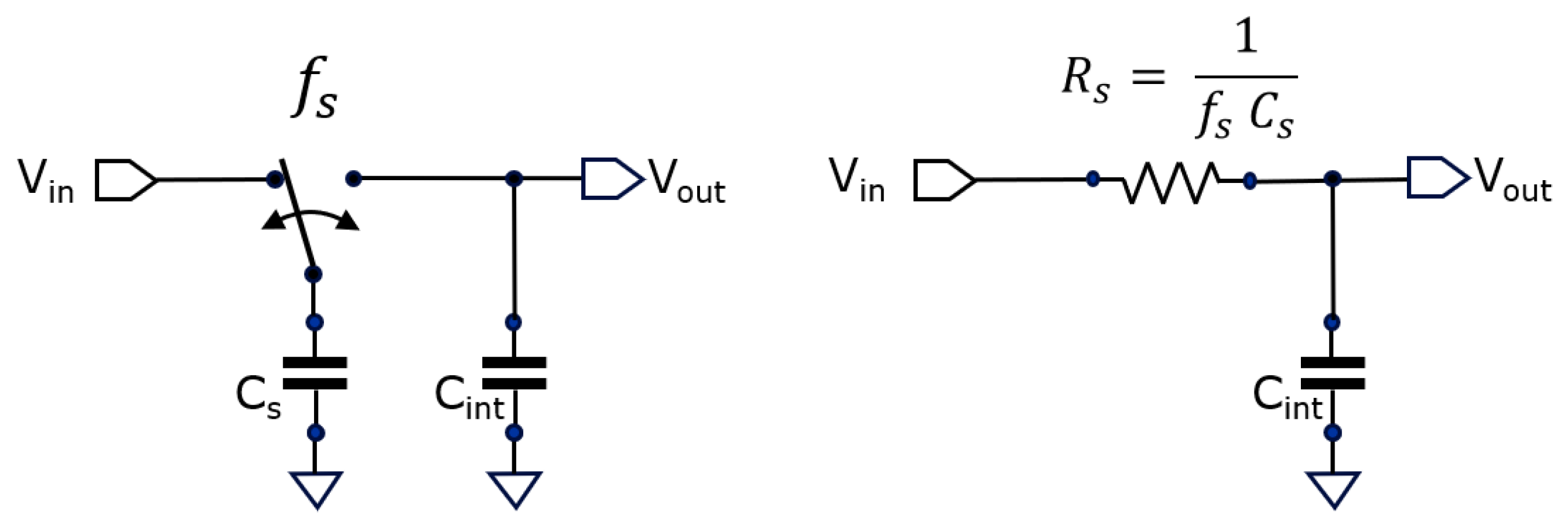
The corner frequency of this low-pass filter is given by:
whereby represents the switching frequency of the switch. Notice that this circuit is the same as an EMA averaging stage. However, this time a regular switching is applied instead of sampling at the occasion of each new sample. Similarly, an averaging number can be attributed to this switched capacitor low-pass filter based on equation (4). A nicety of this type of low-pass filtering is the fact that its corner frequency can be varied in time by varying the switching frequency , something we use for optimizing camera operation further on.
2.3. Analog Counter for Counting Photons
Another textbook circuit is the analog counter, similarly based on switched-capacitor operation shown in Figure 5.
In this case, a pulse on the Reset input resets the voltage on the capacitor Cint to 0 V, at the start of the counting process. At each count event, the switch is toggled. Vo shows an exponential step-like voltage increase over the number of counts; by using the tangent at the start of the slope, the value of Cint/Cs can be constructed graphically. This is similar to finding the RC-time constant in the case of charging a capacitor C through a resistor R.
3. Correlation-Assisted Direct Time-of-Flight (CA-dToF) Principle
In this section, we assume that the available averaging level is much greater than the number of photon triggers detected during a subframe; which is also the case for the indoor experiments of the next section. This assumption has the advantage that a simple comprehensive analytical model can be applied for estimating the precision of the distance measurements. First, the operating principle is explained, and then the accuracy and precision of the depth sensing method are discussed.
3.1. Operating Principle
To achieve a high averaging level, we use a cascade of two averaging stages. The first averaging stage samples at each SPAD trigger (with navg1 = 200), the second is operated as a low-pass filter with a variable switching frequency and with navg2 = 400. These two averaging numbers are used for the simulations below and measurements further on. This brings the in-pixel AA to the product of the two: AA = navg1 × navg2 = 8×10⁴.
In the example case below, the number of incoming triggers within a subframe is less than AA and we assume that we get unharmful over-averaging because the number of ambient photons per subframe (A) and that of signal photons (S) are spread uniformly enough.
Figure 6 shows the two correlation voltage waves (left) generated in the camera. Instead of orthogonal sine and cosine waves for correlation, we use the shown triangle waves (TCOS and TSIN). These are also orthogonal but have the advantage that they can be generated on-chip using simple current sources.
The voltages oscillate between 100 mV and 900 mV, a range in which NMOS transistors (in a 180-nm CMOS technology) operate as pass-gate switches. Assuming 500-mV as the center voltage, the estimated distance can be calculated as follows:
where, Γ is the unambiguous distance (= Tcycle × c/2), which is 6 m in this cycle period (Tcycle = 40 ns). When using the sine and cosine wave, the arctangent function would appear in the depth estimation.
In the simulation of Figure 7, there are 125k cycles of 40 ns; from the laser pulse that is emitted at the onset of each started cycle, only one signal photon (on average) returns after 18 ns from the scene for every 100 cycles, and one ambient photon (on average) for every 25 cycles, following Poisson distribution. Per subframe, S =1250 (on average) and A = 5000 (on average). The ambient to signal ratio (ASR) equals A/S= 4. Left in the figure, the signals VQ1 and VI1 are updated at each incoming trigger, originating from both A and S photons. Because the number of ambient triggers is approximately four times greater than signal triggers, and randomly occurring within Tcycle, the signals exhibit significant noise. On average, the ambient triggers pull the voltage toward the 500-mV midpoint. In contrast, one out of every five triggers are signal photons, located at 18 ns within Tcycle, as indicated in Figure 6 (left). Each such signal event pulls VQ1 toward 580 mV and VI1 toward 180 mV. In the absence of ambient light (A=0), VQ1 would stabilize at 580 mV and VI1 at 180 mV, yielding a total amplitude of 400 mV. However, because ambient triggers occur four times more frequently and tend to shift the signals toward the 500-mV midpoint, the contribution of the signal triggers is effectively reduced by a factor of 5, similar to a ratio division with resistors. As a result, VQ1 fluctuates around 516 mV, VI1 around 436 mV, and the overall amplitude is reduced to 80 mV, i.e., by a factor of . To better recover these voltages, one can look to VQ2 and VI2 that effectively average out the noise but leaving the 80-mV signal intact.
This amplitude reduction is an inherent part of the charge-sharing mechanism in the first stage. The average voltages deliver a depth estimate. The amplitude gives an idea of the ASR. Note that a very large ASR can reduce the amplitude so much that the quantizing of the subsequent ADC becomes a limiting factor. But as long as that is not the case, a large variety of values for A and S can be present in the scene, while the amplitude of the signal still provides a good indication as to how meaningful the signal is; it can thus serve as a confidence measure.
Very conveniently, the averaging system can never saturate and as such, increasing exposure time is never harmful. This is a key advantage of averaging compared to integrating, and this fact is demonstrated further on in the measurements showing a range of ~3 orders of magnitude to choose the exposure time from without running into saturation (Figure 14). Additionally, Figure 15 demonstrates a variation in ASR from 0.2 to 66.
Concerning the choice of the low-pass corner frequency : the lower we choose this frequency, the better the precision will be. However, taking this frequency too low generates considerable spillover from the previous measurement frames, which is detrimental to the measurements’ accuracy. When performing single sub-frame imaging, only a less harmful distance image lag occurs. It is, however, the intention to achieve frame-independent measurements. With switching frequency fs = 80 kHz, and navg2 of 400, one RC-time, will be navg/fs = 5 ms.
To avoid waiting for 5 RC-time periods (25 ms) for convergence, and to achieve accuracy better than 1%, we choose to speed fs up during the first 40% of the exposure period by setting the switching rate to 800 kHz. This is enough to accelerate convergence and to get VQ2 and VI2 to their approximate end-values quickly, leaving time for the remaining 60% of the period to average out the noise, strongly improving precision.
In Figure 7, one can observe that during the first 40% of the period VQ2 and VI2 strongly try to catch up with the changes in the (noisy) first averages VQ1 and VI1. And when the switching frequency is reduced to 80 kHz, their updates are much more conservative. In the indicated estimated (phase) delay at Figure 7 (right), first a quick “reset” towards the 18 ns ground-truth occurs. Then, smaller adjustments in the direction of the ground-truth happen, improving both accuracy and precision.
3.2. Depth Precision Model
The analytical model discussed in the previous publications [6,7,8], only considered limited averaging capability in-pixel, leading to a relatively complex expression for the distance standard deviation (STDV), or depth precision. A comprehensive analytical model can be derived since large averaging can now be achieved in-pixel.
Specifically, we consider the case in which the total available averaging exceeds the number of photon triggers within a measurement subframe (AA > A+S). Under this assumption, a simplified analytical model is derived by treating the averaging as effectively complete. This assumption is justified because the incident photons are statistically distributed across the measurement subframe, ensuring that both ambient (A) and signal (S) triggers contribute to the averaging process. Such full averaging is, in fact, realized with our camera in indoor scenarios presented in the following sections.
3.2.1. Use of Multiple Subframes
In practical cases, multiple subframes are captured to improve depth sensing quality. Therefore, the total number of signal and ambient numbers, and , play a role in determining the depth precision:
whereby, and are the average number of signal and ambient photons in a single subframe and constitutes the number of subframes that play a role in the averaging.
For instance, in the case of a differential measurement, = 2; when four phases are employed, = 4. Furthermore, if neighboring pixels are considered for spatial filtering, this number increases further (by ×4 in the one proposed in Section 5.3).
3.2.2. Effect of Laser Pulse and SPAD Timing Jitter
Received signal photons (S) are spread in accordance with the emitted laser pulse width and are further broadened by the SPAD’s timing jitter based on RMS addition. Their common STDV will be reduced based on the total number of signal photons involved as follows:
whereby, is half the laser pulse width. The effect of the SPAD’s timing jitter can be neglected with a laser pulse width that is substantially longer.
Few photons are needed to reduce the effect of the laser pulse width to below one percent. Consider a commercially available VCSEL array generating 2-ns wide pulses to illuminate the scene, 25 signal photons reduces the jitter from 1 ns down to 200 ps jitter, corresponding to 3 cm variation, or 0.5% on an unambiguous distance of 6 m. The assumption that the laser pulse has a Gaussian shape is typically not met; in our experiments, it has more of a top-hat shape. Still, the narrowing of the time/distance spread is somewhat in accordance with Equation 10.
The received signal photons (S) also induce shot noise which generates noise on the two averaged voltages. However, if these are sampled simultaneously (like in Figure 6), these noise components are correlated and their effect on the distance is cancelled or strongly reduced; therefore, we consider this effect as second order.
3.2.3. Effect of Ambient Light
Ambient light photons are an important factor in the noise that leads to the distance STDV. The signal to (uncorrelated) noise ratio is:
where the divide by 3 comes from the effective value that a triangle wave generates when averaging according to the root-mean-square (RMS) principle. When using sine and cosine waves, the divisor would be 2. From the partial derivative of the distance one can deduce that:
or by substituting Equation (11) into Equation (12) one gets:
The total STDV on the distance is calculated using the RMS method,
In case there is little ambient light present, the effect of the laser-pulse width will dominate. Further refinement of these calculations shows that deviations occur in the triangle wave corner cases (at 0, 10, 20, and 30 ns in Figure 6 left) due to rectifying effects. These effects are relatively small when the laser pulse width is small compared to the cycle time; as such, we consider it a second-order effect.
3.3. Accuracy Considerations
The accuracy of depth measurements can be affected by several factors. Imperfections in SPADs such as dark counts, afterpulsing and deadtime are some of their inherent limitations affecting the measured distance accuracy and precision. In addition, non-idealities in the VCSEL array and its driver, as well as the presence of multiple optical propagation paths, introduce further sources of error that degrade measurement accuracy. In this section, we address these challenges and their effect on CA-dToF.
3.3.1. Effect of Laser Pulse Shape
The shape of a commercial VCSEL array pulse is closer to a “top-hat” than to Gaussian pulse. CA-dToF estimates the position based on the center of mass (CoM) of the laser pulse, in the time domain. When the light source changes temperature or ages, the laser light output pulse distribution may change, leading to a CoM deviation that can be regarded as a general distance offset for the full array.
Further, in the triangle wave corners, some level of rectification occurs, leading to a deviation from the real CoM, generating a cyclic error. This cyclic error is also in proportion to the laser’s pulse width. To gauge the importance of this error, we further characterized it with the camera demonstrator (Section 5.4).
3.3.2. Effect of SPAD’s Non-Idealities
A first element to consider is the SPAD’s dark count rate (DCR). DCR triggers are uncorrelated with the laser pulse emission and thus behave similarly to triggers from ambient light photons. Some SPADs may exhibit a significant high DCR, and like with very high ambient photon rates, this is discoverable by observing the amplitude of the averaged signal. When using spatial filtering, a singular high DCR SPAD is seamlessly included with less impact on the estimated distance outcome (Section 5.3).
Afterpulsing is correlated with delayed triggers from the received laser pulse, leading to accuracy errors. This must be avoided by any available means. The likelihood and delay of the afterpulsing will influence its impact.
The SPAD’s deadtime can introduce two major effects, as described in more detail in [8]. The first one is shadowing of the ambient photons: if S signal triggers happen often, e.g., every Tcycle, then during the subsequent deadtime, ambient photon triggers are suppressed; thus, the assumption of equal spread of ambient triggers is no longer valid. Similarly, the deadtime can also obstruct the triggering from signal photons arriving quite immediately after a previous signal photon trigger. This is referred to as pile-up. In both cases, objects appear closer than ground truth, leading to an accuracy error. If these issues become relatively important for an application, an approach can be taken whereby multiple SPADs are dedicated to serving one pixel, mitigating the deadtime effects, e.g., 2 x 2 or 3 x 3 SPAD cluster topologies can be implemented. In this case each SPAD can have its own non-overlapping clock generation, operating independently, yet they can all average out on the same Cint. In the camera demonstrator, the number of photons received per cycle is limited so that deadtime effects can be considered negligible.
3.3.3. Multipath Errors
Multipath is an important element in systems that work on phase estimation. When there are multiple ways in which the pulsed light can travel and reach a pixel, complex vectors add up, and the phase of the vector sum generates the estimate of the distance. The larger the contribution of the interferer to the victim, the more the distance outcome deviates from the real distance. This crosstalk is more detrimental when the victim has a small amplitude, like distant and/or with low-reflective objects. The interfering photons may follow different paths, such as when having (i) double reflections in the corner of a room, (ii) when having reflections on a semi-transparent object, like a glass door, or a glass bottle, (iii) when having light received from both an edge of an object, and, e.g., a more distant wall. The last condition can however be treated further-on in the image processing chain. Multipath problems are known in iToF systems. Likewise for CA-dToF, they limit the depth accuracy.
4. Camera Demonstrator
In this section, the hardware is described that was developed to demonstrate the operation of CA-dToF on a large image sensor. A custom chip was designed in 180-nm high-voltage CMOS technology (from X-Fab), utilizing foundry-validated SPADs. Testability was a main design target, with internal option bits allowing many ways of sensor operation. First, the pixel will be described, followed by a view of the overall camera demonstrator.
4.1. Pixel Circuitry
A single SPAD per pixel has been implemented. It is passively quenched, with an R0 of 350 kW followed by two capacitors (28 fF) in series to handle the high voltage (C0 = 14 fF). This AC-coupling was the only option for making an array-type demonstrator in the given technology. At the ToA two non-overlapping clocks (F1, F2) are generated for toggling the photon counter stage, the TSIN and TCOS first averaging stages simultaneously. The second stage averaging filters have their non-overlapping clocks (F3, F4) switched with a settable frequency, like in the simulation (Section 3.1).
The analog photon counter is available for grey-image capture and depth-model verification. Its voltage V0 goes exponentially towards 1V (Fgure 4), however, we limited its use up to 2/3 of the maximum 1V because the count fidelity worsens close to the asymptotic 1V level. At 2/3 is when ~1715 photons have been counted, which we define as the counter’s full-depth.
Figure 8.
The pixel circuit has a non-overlapping clock generator, a photon counter, and two-stage averaging for the sampled triangular TSIN and TCOS signals.
Figure 8.
The pixel circuit has a non-overlapping clock generator, a photon counter, and two-stage averaging for the sampled triangular TSIN and TCOS signals.
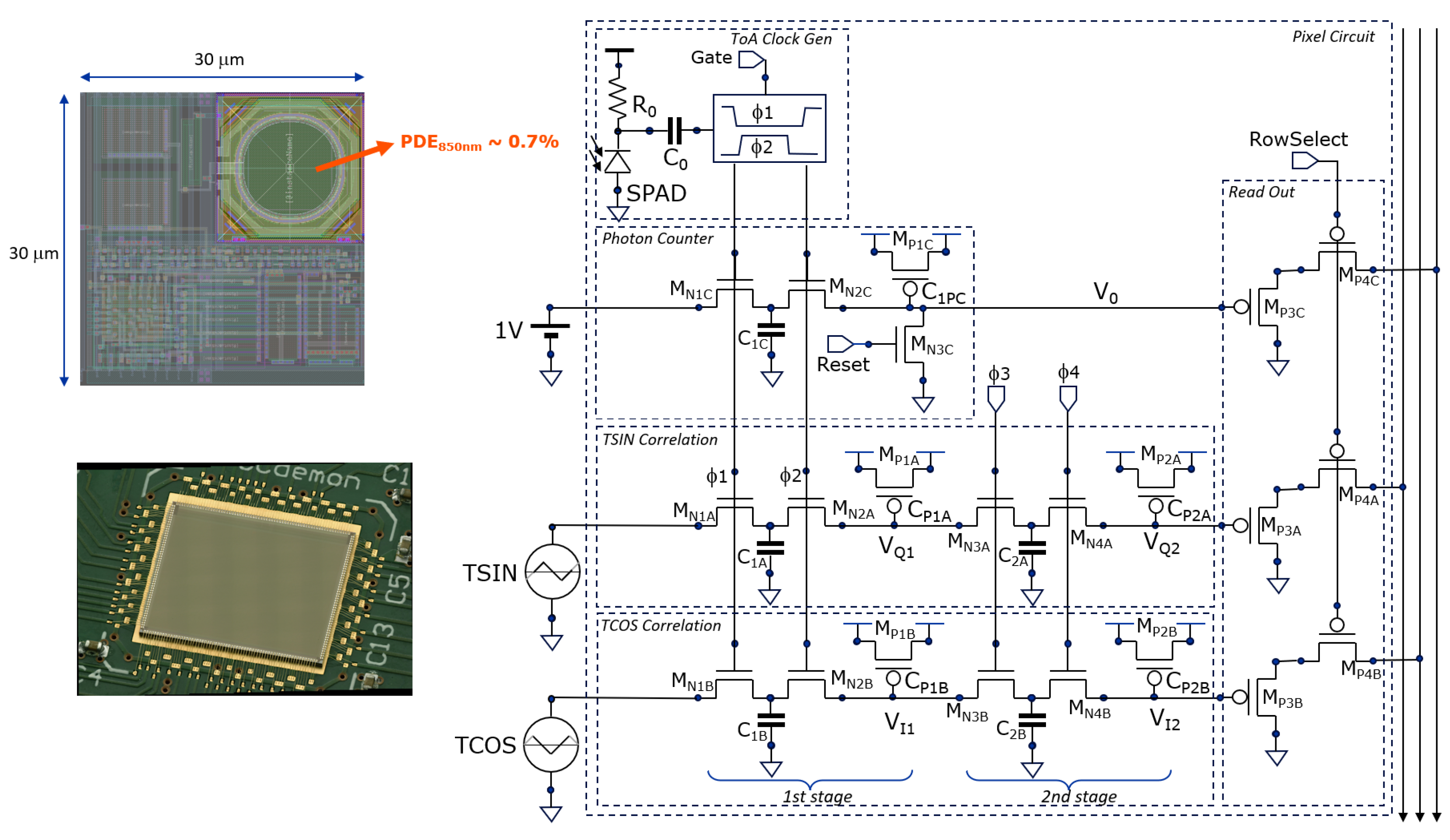
Further, we use the photon statistics to calibrate the conversion factor between the ADC’s digital number and the incident number of photons, knowing that we operate in a shot-noise limited regime. There is a measured statistical spread of ~ 4% over the counter gain of the pixels due to the statistical variation on the parasitic Cs in the photon counters.
For a simple on-chip implementation (Figure 7), triangular signals (TSIN, TCOS) are applied instead of the sinusoidal signals. A nanosecond window-gate is present that allows the system to operate as a high-speed time-gated fluorescence lifetime camera [9], not discussed here. The total pixel area is 30 × 30 μm2 including SPAD (Ø = 10 μm), delivering a fill factor of 8.7% and hence a low PDE of ~0.7% at λ = 850 nm. Readout is done through PMOS voltage followers with PMOS select switches.
4.2. Camera and Image Sensor Circuitry
The setup was developed as a proof of concept for the proposed averaging principles and triangle waveform generation, offering a high degree of configurability. For example, the column ADC can be configured for 8-, 9-, 10-, or 11-bit resolution, and its conversion slope can be selected to occur in steps at 50, 100, and 200 MHz. Many of the internal signals, including the triangle wave voltages, can be verified on the oscilloscope via the internal multiplexers connected to test pads.
Figure 9 (right) shows the camera architecture together with the image sensor circuit. The FX3 microcontroller forms the interface between the PC and the image sensor to transfer the image data over USB3.0 and to provide clock and measurement arbitration signals to the sensor. The FX3 does not perform image data manipulation; this is done on the PC.
From the 50 MHz clock provided by the microcontroller, the image sensor generates a 40-ns cycle (Tcycle) and, through a current-starved delay line, 64 subdivisions of 625-ps periods are defined. A delay-locked loop regulates the current so that these 64 steps align with the 40 ns cycle. Each of these subdivisions can be tapped for controlling cycle-related elements. These cycle-related elements are (i) the start and (ii) the end of the laser pulse, the (iii) corner points of the triangle waves, and (iv) the position (start and stop signals) of the (optional) SPAD gating of the pixels (not reported here but used in [9]).
The laser driver (EPC21603) is off-chip and driven by an LVDS output to avoid supply bounce correlated with the laser pulse. The VCSEL array used in the experiments is from OSRAM-AMS (EGA2000-850-N). A 16 mm/F1.6 VIS-NIR lens (Edmund Optics #67-714) was used with a bandpass filter (850 nm center, 50 nm FWHM). The second stage average switching rate fs, which may be varied over time (e.g., 800 kHz and 80 kHz) is interrupt-driven by the FX3 microcontroller and its propagation (Φ3, Φ4) over the full array is done by the image sensor circuitry in a rolling wave mode, i.e., from row to row, to spread the current drawn from the power supply. During subframe readout periods, fs is halted to avoid clock feedthrough in the output values. The FX3 controller also controls when the photon counters are reset, the gate is actuated, read-out happens, laser is enabled, etc....
5. Operation of the CA-dToF Camera
In this section, we show various operational modes, starting with differential operation, followed by a dual frequency approach without and with spatial filter application at the PC level. Two additional experiments show that the system doesn’t saturate at longer exposure times, and that it can handle a large range of A and S photons within the same image. A first attempt to evaluate a higher A operation with a moving wall in various ambient light conditions is also included.
5.1. Differential Operation Using (0°, 180°) Phases at 25 MHz
In the subsequent demonstrations, we make use of (quite long) 20-ms exposure subframes to compensate for the low PDE. Figure 10 demonstrates the operation at 25-MHz demodulation, giving a 6-m unambiguous range. During each subframe, a VCSEL light transmitter, positioned close to the lens, pulses floodlight to the scene. Two subframes are recorded (0°, 180°), performing a differential measurement, to cancel offsets from the source followers and column ADCs. Distance is calculated using the following equations,
whereby the common voltage is conveniently eliminated. Since 2 subframes are used, . Only the position of the laser is changed (0°, 180°) between the two frames, and thus the measurement depends only on small signal differences linked to the difference in laser pulse position. This makes it very robust and independent of absolute values. For example, the vertical position and the amplitude of the TSIN and TCOS waves become relatively unimportant. We can set them to oscillate between 100 mV and 900 mV, but also, between 200 mV and 600 mV yielding same depth estimates of the objects in the scene.
Figure 10 shows a scene with some challenges as a test environment: (a) is a mannequin, (b) a whiteboard, (c) are retro reflectors for testing dynamic range, (d) a cabinet in the corridor and (e) is a box with black & white stripes for testing color dependency.
In the grey image, the first 32 columns have been reserved for some special experiments, not considered here. This image is taken with and without the laser enabled, in that way providing a method for deducing A and S. Choosing the grey image exposure period manually allows us to avoid saturation whilst still having enough photons to give a somewhat reliable number for the darker scenes. Taking into account the exposure period ratios (of the grey subframe and of the depth subframes), an accurate estimate for the depth-subframe’s A and S number of photons can be extrapolated (assuming a fixed laser output amplitude).
The recorded Q2 and I2 images (Figure 10 bottom) give a mix of grey and phase information. However, when used in accordance with Equations (15, 16), they deliver a depth map in the 0-6 m range, effectively canceling the color dependence (grey value).
The magenta curve on Figure 10, upper right, the estimated distance for each frame, whilst the black curve is an average over 100 measurements, for measuring accuracy and for the calculation of the distance STDV. The modelled STDV, based on Equation 14, and on the extrapolated A and S, can now be compared with the measured STDV. The results show a good agreement, and a relatively good precision of 0.5% is observed at the center of the image. There is no depth color dependency noticeable at position (e).
The retro reflector is giving 15 times increase in signal photons and 4 times increase in ambient photons (at column 200). The depth estimate is not affected, however improvements in modelled and measured STDVs are clearly noticeable.
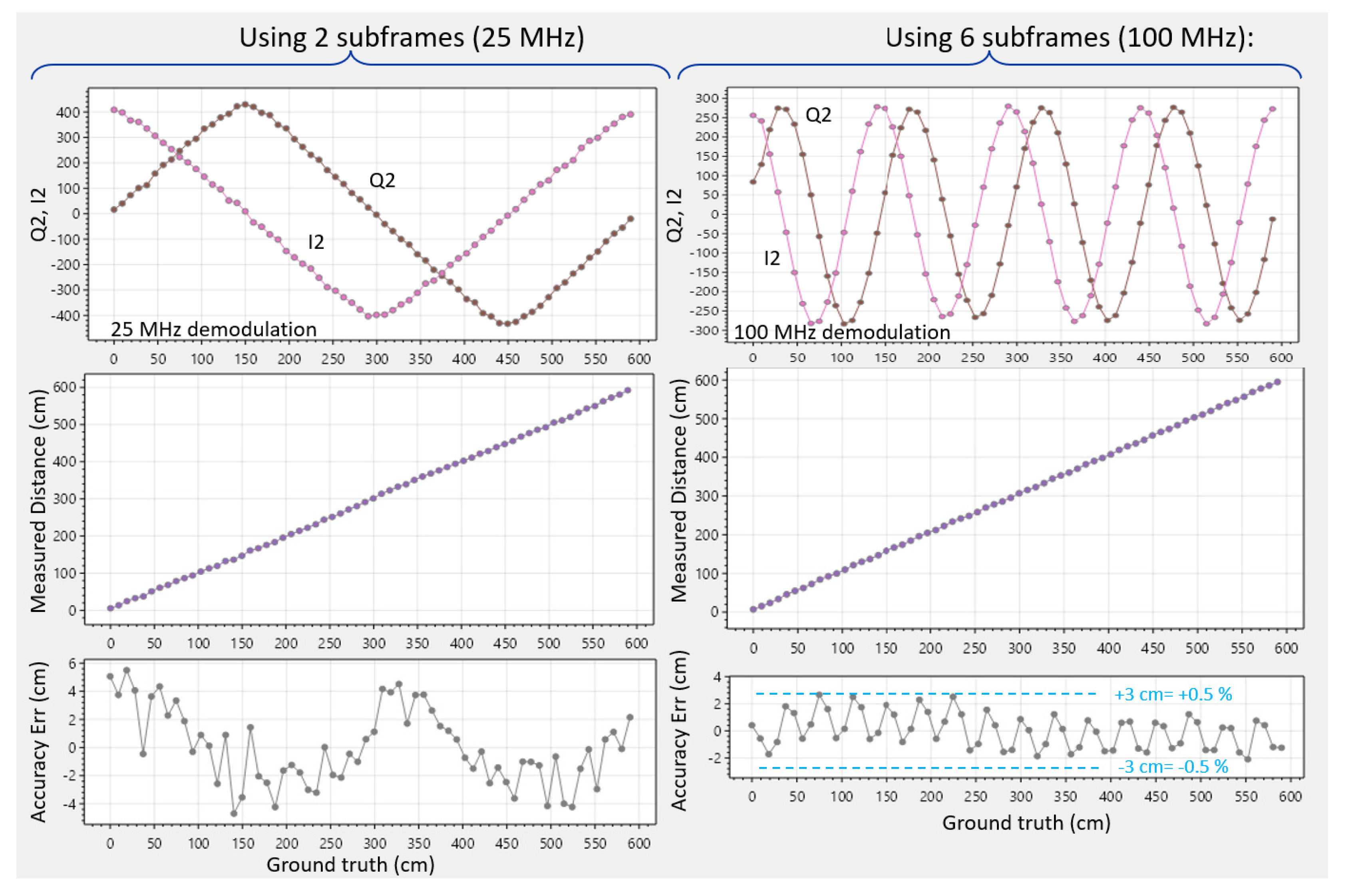
5.2. Dual Frequency: (0°, 180°) Phases at 25 MHz and (0°, 180°, 90°, 270°) Phases at 100 MHz
In Figure 11, a rough initial distance estimate is made at 25 MHz (with 0° and 180°) (similar to Section 5.1), followed by a much more precise 4-phased estimate at 100 MHz, similar to [4] in iToF. Tcycle remains at 40 ns; the laser remains pulsed at the same 40-ns intervals; however, the triangular wave generators are directed to oscillate 4 times per cycle, based on four times more corners provided from the 64 divisions. The second measurement now has a four times reduced unambiguous range of Γ = 1.5m, and an (from the 4 phases). The 6-m range is thus combined with a much-improved precision (4 ×better in theory) and accuracy, at the expense of a 3 times lower framerate.
5.3. Nearest Neighbor Spatial Filtering Operation
In Figure 12, the camera conditions from Figure 11 are reused, but the outcome is followed by spatial filtering in post-processing on the VQ2 and VI2 using 50% of the pixel’s nearest neighbors and 25% of its diagonal neighbors. Since the distance is now based on a 4-fold number of measurements compared to the previous example (), the predicted STDV is further reduced by a factor of two. Also, the measured STDV was reduced by two, but an unknown issue was preventing the STDV from reducing below 4 mm.
The measured STDV is however quite good, percentagewise (0.1%). Another way to visually recognize this, is that even with the color scale cycled 7 times over the 6-m range, little noise in the 3D depth picture is visible (left).
It is important to consider that spatial filtering can be done either at the (I, Q) level or at the distance level. By doing it at the (I, Q) level, a pixel with less amplitude automatically reduces its own weight. This was confirmed at a pixel with a very high DCR (a so-called screamer): its low Q and I, effortlessly reduced its weight through averaging (not shown). This seamless weighting will not occur should the distances be averaged.
A drawback of spatial filtering is that on sharp edges, the effective spatial resolution is somewhat reduced (which has been noticed but not shown here). But the fact that accuracy and precision are improved significantly makes it worth implementing. Using multiple pixels and multiple phases in the evaluation of the distance leads to accuracy improvements and reduces variability on every level of the analog signal chain. An accuracy detail is on the bottom right, Figure 12: the distance to box (e) with the white and black stripes appears flat, as it should: the measurement deviates from a straight line by only +/- 1 cm (+/- 0.16%). Note that this is accomplished without any calibration, neither at the pixel nor column level.
5.4. Evaluation of Cyclic Errors
To investigate the error generated by various sources on the distance measurement, we have made a test procedure that can easily measure accuracy errors over phase variation, Figure 13. Any pixel in the image can be selected, having its particular A, S, and distance conditions.
We cycle the laser pulse through the 64 positions and measure Q2 and I2 for each phase and plot associated distance. Through this demodulation, we sample the triangle waves at the given ASR condition. In each triangle corner, there will be some rounding due to convolution with the laser pulse width.
In our experiments, the laser pulses were ~2 ns FWHM. Using Equations 15 and 16, we get a distance between 0 and 6 meters. The deviation from the ground truth is the accuracy error, revealing limitations to the depth estimation principle. Measuring the ground truth versus distance in real circumstances (as is done in Figure 16) takes more time and requires a specific setup, whereby the effect of phase variation and signal S intensity variations are varied simultaneously. S reduces strongly with the square of the distance. In that way, a mix of effects is recorded, which is unfortunate, because when an error occurs, it can’t be uniquely attributed to the phase or S variation. The advantage of only cycling the laser pulse position is that now very quickly cyclic errors due to phase errors can be uncovered independently of the S variations.
Figure 13 (left) shows the cyclic error with a differential measurement. Q2, I2 show slightly rounded triangle corners due to convolution with the 2-ns laser pulse. This is with a pixel at 370 cm depth, A and S at ~1000 photons per subframe, ~1 klux of ambient light. When cycling through the various laser positions, additional averaging is applied in post-processing to study accuracy with reduced temporal noise. The error is +/- 6 cm, or +/- 1%. On the right, the case of dual frequency with spatial filtering is tested, revealing the 100 MHz demodulated triangle waves, the derived distance, and its accuracy error. The dual frequency approach helps to improve accuracy to +/- 0.5%. Cyclic errors have 16 oscillations due to the increased frequency. Notably, the demodulated waves have become more sine-like due to the relative increase of importance of the 2-ns laser pulse with respect to the shorter 10 ns triangle period. This effect was aggravated experimentally by lengthening the laser pulse confirming the assumption (not shown). Application of a shorter laser pulse on the other hand was not possible with the used laser driver/VCSEL combination.
Interestingly, a few pixels in the array expressed increased cyclic error in the differential measurement. This was attributed to a difference in amplitude between Q2 and I2 of the pixel involved (for example due to different PMOS transistors used in the voltage followers). Fortunately, with 4-phased measurements (either with dual or with single frequency), due to the combinations of the various sub measurements, the aggregated amplitudes become the same by construction, and hence this source of cyclic phase error gets automatically largely compressed. For improving accuracy, 4-phased operation is thus helpful.
5.5. Exposure Time Freedom
Whilst experimenting with the camera under various light conditions, the exposure time for the grey-imaging photon counter required careful setting to avoid image saturation. Conversely, the true benefits of the CA-dToF are highlighted by its non-saturation behavior, since the averaging process never saturates I2 and Q2. Consequently, one is free to choose an exposure time and set the toggling rate(s) in accordance with the principle explained in Section 3.1.
To demonstrate this resilience, we selected a pixel at a distance of 410 cm and under an illumination condition of A≈S, at 1 klux ambient light. Differential measurements were done with a single frequency (25 MHz), with the spatial frequency filter applied (), and the exposure time for the depth measurement being varied over nearly 3 orders of magnitude: from 100 ms to 80 ms (limited by a software bug). The accuracy was not impacted (+/- 1%). These results are shown in Figure 14.
Figure 14.
Experiment showing variable exposure time for depth sensing, from 100 us to 80 ms. The measured average A and S (bottom) are indicated, and measured and modeled STDV, based on A and S (top). Depth variations remain withing +/- 1% (middle).
Figure 14.
Experiment showing variable exposure time for depth sensing, from 100 us to 80 ms. The measured average A and S (bottom) are indicated, and measured and modeled STDV, based on A and S (top). Depth variations remain withing +/- 1% (middle).
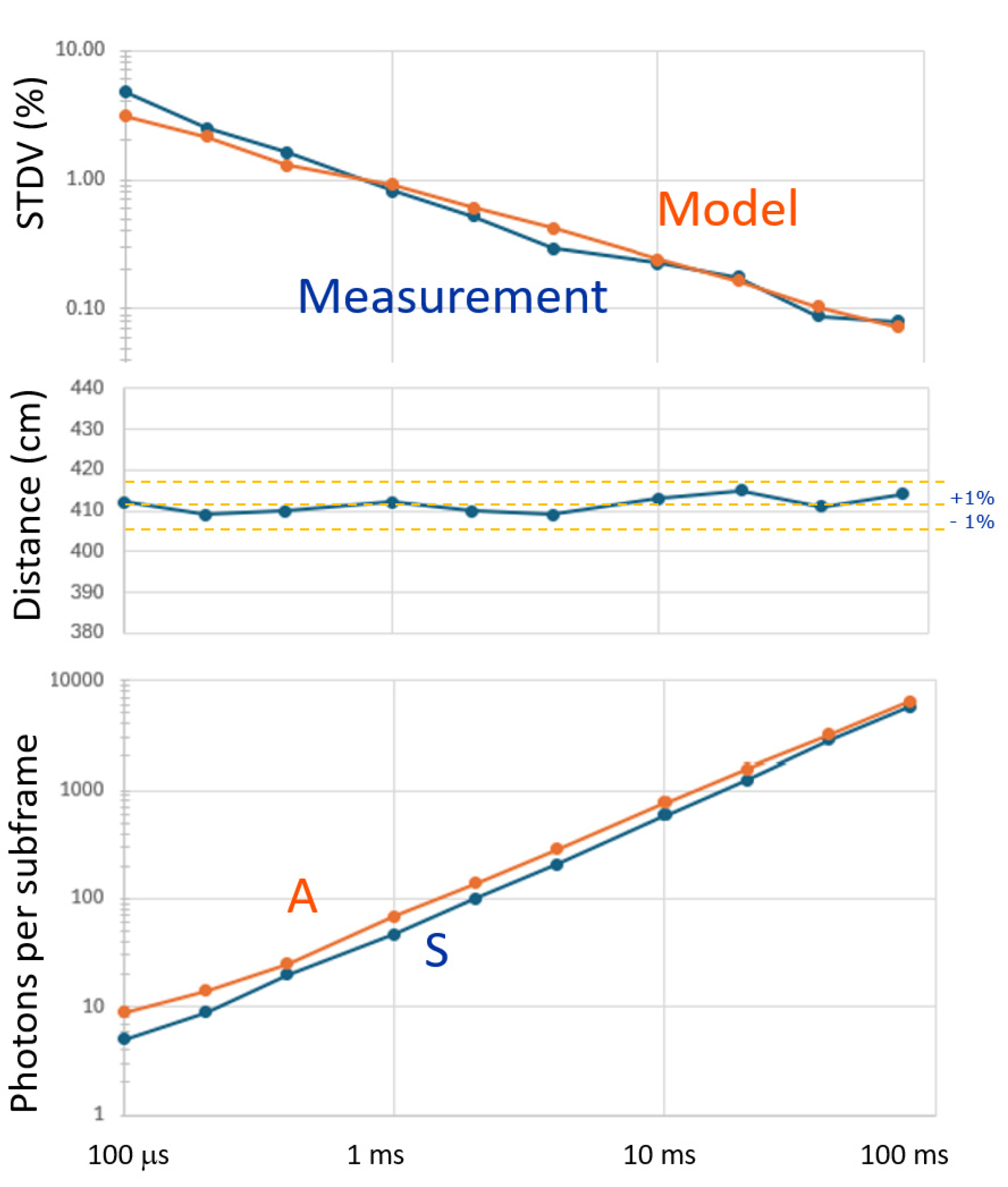
During the measurements, the ambient weather conditions slightly changed, and the ambient light was almost twice as much during the short exposure times. Nevertheless, the distance remained at 410 cm (+/- 1%) over the various exposure conditions. The measured standard deviation is well in accordance with the modeled one. The shortest exposure time is an interesting case: per subframe, each pixel receives only S = 5, and A = 10 photons. Still, an STDV of 5% is reached, after spatially filtering (as in Figure 12).
This demonstrates one of the true benefits of CA-dToF. By not-binning the incident photons (and thus not confusing their ToAs), by operating shot-noise limited, and effectively applying the CoM on the received signal photons, a system is created that starts giving reasonable depth estimates from a low number of signal photons S onwards.
5.6. Use Under Higher Ambient Light Conditions
Another experiment worth performing is to vary the ambient light over a large range, keeping all other conditions the same, including the object distance. To study this, we selected a pixel at a distance of 200 cm. The light of a dimmable halogen spot was focused on the area of interest, and with 10 different ambient conditions (varying A), the curves of Figure 15 were recorded. Four-phased measurements were done at a single frequency (25 MHz), the spatial frequency filter was applied (), and the exposure time for the depth measurement was fixed at 2 ms. The lowest ambient condition was A = 251 and the highest was 20066. The applied laser signal was fixed. Note however that the measured value decreased from S = 630 (when having low ambient) down to 303 (at high ambient). Together, ASR ranged from 0.25 to 66.2. The changes in measured distance stayed within +/- 1% (middle graph), however, a tendency is observed that for higher ambient, the object appears to be closer. The standard deviation increased with more ambient light, as expected.
Figure 15.
Experiment with an increasing amount of ambient light from A=251 to 20066 photons per subframe (bottom). Indicated are A, S and ASR (bottom). The measured distance (center) and the modeled and measured STDV (top).
Figure 15.
Experiment with an increasing amount of ambient light from A=251 to 20066 photons per subframe (bottom). Indicated are A, S and ASR (bottom). The measured distance (center) and the modeled and measured STDV (top).
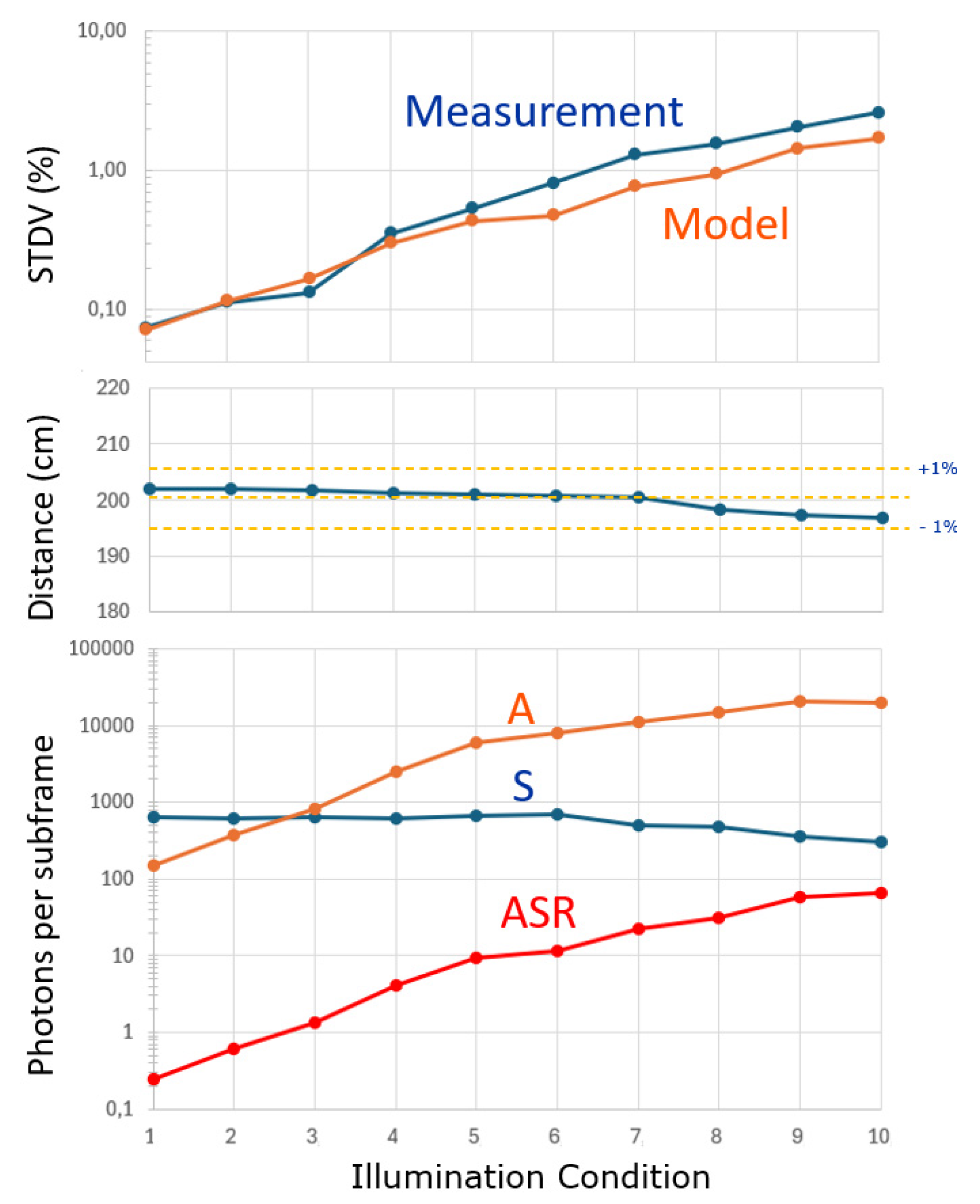
The STDV model still conforms, however, the measured outcome is somewhat worse at higher levels of ambient light. The sum (A+S) remained well below the AA = 8×10⁴ for all conditions. Since the ASR reached relatively high values, the ADC was set to the 11-bit resolution needed to achieve enough resolution at the lower output voltage levels reached during this measurement.
Measurements discussion: The fact that S reduces with increasing A could be attributed to the deadtime of the SPAD. Further, the object appearing closer at a higher ambient can be attributed to the mentioned shadowing effect [8]: signal triggers that prevent ambient triggers in their deadtime, and therefore, the ambient triggers are no longer evenly distributed. Nevertheless, this demonstrates the power of averaging: even though the ambient light is 66 times stronger than the reflected laser light, it does not significantly affect the measured distance.
5.7. Moving Wall Experiment
A ground truth experiment was performed under four ambient light conditions. Considering the low PDE, an additional VCSEL array was built-in, illuminating the scene with an average light power of 580 mW at 850 nm. Calibrated artificial sunlight was projected on a wall that could be positioned in the full unambiguous distance range. Four levels of ambient light (0, 11.5, 17.3, and 22.9 klux) were selected for the experiment. The subframe exposure time was 25 ms, the triangle frequency was 24 MHz and 96 MHz (for 6 phases), the spatial filtering was applied. Using switches, a subsequent third averaging stage was included in the circuit (not shown in the schematics of Figure 8), in principle allowing averaging of 200 x 200 x 200 = 8 x 10⁶ samples. The toggle frequencies of the second and third stage were set at 80 kHz and 0.8 kHz. Since the experiment was done in a limited time frame, performative conclusions shouldn’t be made yet.
Figure 16.
Estimated distance versus ground truth (top). Error on the distance (center), STDV of the estimated distance (bottom).
Figure 16.
Estimated distance versus ground truth (top). Error on the distance (center), STDV of the estimated distance (bottom).
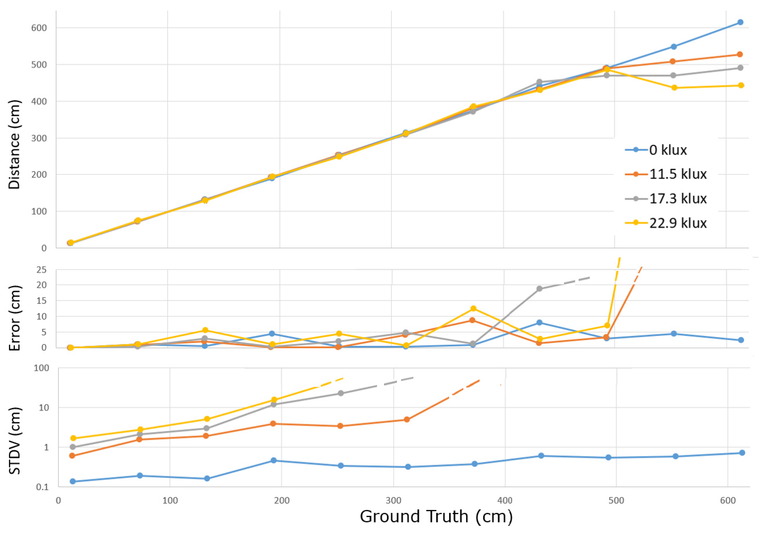
Nevertheless, some observations can already be made. Since the averaging can’t saturate, exceptionally short distances can still be measured correctly (down to ~7 cm). At longer distances, due to the poor SPAD’s PDE, and the quadratically reducing number of signal photons S for longer distances, the STDV gets out of hand (in several percent and then 10’s of percent), which triggers two failure modes leading to large accuracy errors (> 4 m). The first failure mode is that when being close to the end of the unambiguous range, the phase wrapping suddenly gives a very short distance, which is detrimental for the average distance calculation. Further, when the low frequency measurement delivers a distance error (in one of its measurements) of more than 75 cm, the algorithm picking the distance out of 4 may pick the wrong one, which then yields an error of 1.5 m, also jeopardizing the average distance calculation. When the standard deviation is high in the base frequency, it may thus be a safe choice to stick to the single frequency approach. Additional experiments need to be conducted on higher ambient light levels with moving walls, using additional laser light, before more final conclusions can be drawn on the performance of the present demonstrator in higher ambient light situations.
5.8. Additional Performance Parameters
The subframe rate with 20-ms depth exposures was 24 fps. The differential frame rate was thus 12 fps for Figure 10, and the systems with dual frequency and 6 subframes were 4 fps (Figure 11 and Figure 12). Besides the long exposure time, the dataflow and many other time-consuming elements can still be optimized/parallelized. The column ADCs were running at 100 MHz, with a 10-bit resolution, except for in the moving wall experiment where 11-bit resolution was used.
Concerning the image sensor power dissipation: in the experiments of Figure 10, Figure 11 and Figure 12, the supply for the SPADs needed to deliver 1 mA at 22 V in the case of 1-2 klux ambient light in the frame with excess bias set at 2.4V. Other than the SPAD voltage, the image sensor requires a single supply voltage of 1.8 V (Vdd). Current consumption on Vdd was 61 mA when recording differential frames, and 98 mA when recording at dual frequency, with 6 subframes. The higher current is due to the elevated frequency of the TSIN and TCOS triangle waves. Since the generation of the triangle waves is done by simple current sources and sinks, a comparable power dissipation is reached as when driving a full-swing digital signal over the array. Since the amplitude of these triangle waves is only half the supply voltage, but the current provided from the full Vdd voltage, one can state that providing a single clock signal to the full array at full supply voltage consumes about the same amount as driving two triangle waves to half the supply voltage. Additionally, there is the power consumption for the generation of the non-overlapping clocks; however, the firing of the SPAD itself is consuming much more energy due to its relatively large capacitance, and the potential drop for the charges over the 22 V SPAD supply, instead of over the 1.8 V Vdd supply. The power dissipation needed by the second stage filter that requires the clocks (Φ3, Φ4) to be switched over the full array, can be considered negligible, because it runs at a much lower frequency than the triangle waves.
6. Discussion
CA-dToF, as presented in this paper, operates with a short light pulse that is sent to the scene, whereby received reflected photons are correlated with two orthogonal waves, precisely registering the ToA. The fact that it works (and can only work) with a short light pulse makes it thus a direct time of flight system. The returned short light pulse is thus registered upon arrival. This is in contrast with iToF, whereby the emitted light that traverses the scene is an amplitude wave, which is demodulated after reception by directing each photo-generated electron to one or another (floating) diffusion based on a demodulating signal.
However, since there are also demodulation waves involved, several commonalities with iToF [4] can be expected. Let us thus consider the challenges that occur in iToF and how they relate to CA-dToF:
- One of the challenges in iToF is the cyclic error that occurs when the shape of the modulated laser amplitude wave deviates from the targeted one (typically square or sine wave). This directly translates into a cyclic error behavior and possibly needs calibration. In the case of CA-dToF, the laser pulse is short, and its shape is less relevant. What counts is the CoM of the laser pulse, which, if it changes, leads to a global fixed distance error, not a cyclic error. Additionally, a deviation in the shape of the triangle wave leads to cyclic error. Fortunately, making a controlled electrical shape at 100 MHz is much easier than making a controlled optical wave shape.
- Another element is that most iToF systems use dual-tap receivers and need to perform the demodulation for the 0° and 90° phase in a separate subframe. As a result, laser-light shot noise isn’t cancelled. In the case of CA-dToF, since both ASIN and ACOS waves are sampled simultaneously, and laser-light shot-noise gets cancelled (Section 3.2.2).
- Further in iToF, the ToAs are binned and therefore precious information on the exact ToA is lost, which will lead to an increase in the distance’s STDV. CA-dToF can handle low-light levels quite well due to this, but also due to the fact that operation is shot noise limited: at a level where iToF has not yet surpassed its read-out noise level, a decent distance estimation can already be provided with CA-dToF.
- In iToF, one integrates charges generated by A and S photons, and one has to choose the exposure period long enough in order to accumulate enough signal to be above the read-out noise, but also not too long, to avoid reaching the full well capacity. And this, for all received illumination conditions (variable A and S) throughout the image. Often several different exposures need to be performed to get full image coverage. At edges of a different exposure, stitching distances leads to accuracy errors at the stitch boundary. CA-dToF can’t saturate over large ranges of A, S and exposure times; this is a clear advantage. No calibration, except for the array’s general distance offset is needed: this concerns a single delay value for the full array. In addition, 4-phase operation together with the proposed spatial averaging suffices to largely reduce variabilities, offsets and non-linearities.
- An advantage of the iToF system is that it provides a grey image as well, which is required in most applications. In CA-dToF, a dedicated photon counter needs to be added in the circuitry for grey scale acquisition.
- It is an option in CA-dToF to use the fast-gating system to make the pixels blind for light-pulse reflections during (for example) the first 5% of Tcycle: this can solve the multipath crosstalk induced by a common cover glass. Some of the nearby camera depth range will however be sacrificed.
On the dToF side, several additional considerations can be made:
- dToF is implemented in a complex digital way and requires quite some circuitry, limiting the pixel pitch. With CA-dToF, full resolution, low pitch and low power may become in reach.
- Clustering multiple SPADs per pixel, can be done in CA-dToF. In dToF this leads to a system deadtime that limits depth-accuracy by blocking ToA registrations of clustered SPADs firing simultaneously. However, in CA-dToF by giving each SPAD in the cluster its own non-overlapping clock circuit (Section 3.3.2) this can be avoided.
- Binning of photons (dToF) restricts the depth estimations when having low numbers of signal photons. CA-dToF uses each ToA to its fullest potential, resulting in an optimal CoM situation.
- On the other hand, the noise from ambient photons in the histogramming approach stems from the ambient photons in the histogram bins in and around the observed peak. This helps dToF long range LIDAR systems operate in full sunlight.
- Multipath is not a source of concern in dToF, when leading to multiple separable peaks in the histogram.
7. Future Work and Conclusions
All the performance parameters are subject to much improvement when increasing the PDE from 0.7% to 40%: this can be achieved with an optimized image sensor design using 3D stacking technology. Sub-millisecond exposures can then be reached, frame rates increased, ambient light resistance improved, and power dissipation reduced.
This opens the way to high-resolution CA-dToF depth cameras expected to outperform iToF cameras in several ways. High dynamic range with respect to both ambient and signal light, can then be anticipated. Short distance ranging can be included, and/or cheaper illumination systems can be used in certain applications. Increasing the laser illumination light levels can bring outdoor ranging into reality, with a distance range determined by the applied laser light level.
Funding
This work was partly funded by a VUB university project SRP78.
References
- Bastos, D.; Monteiro, P.P.; Oliveira, A.S.R.; Drummond, M.V. An Overview of LiDAR Requirements and Techniques for Autonomous Driving. In Proceedings of the 2021 Telecoms Conference (ConfTELE), Leiria, Portugal, 11–12 February 2021; pp. 1–6. [Google Scholar]
- ALi, Y.; Ibanez-Guzman, J. Lidar for Autonomous Driving: The Principles, Challenges, and Trends for Automotive Lidar and Perception Systems. IEEE Signal Process. Mag. 2020, 37, 50–61.Author 1, A.; Author 2, B. Book Title, 3rd ed.; Publisher: Publisher Location, Country, 2008; pp. 154–196. Noise analysis.
- Horaud, R.; Hansard, M.; Evangelidis, G.; Ménier, C. An overview of depth cameras and range scanners based on time-of-flight technologies. Mach. Vis. Appl. 2016, 27, 1005–1020. [Google Scholar] [CrossRef]
- Bamji, C.; Godbaz, J.; Oh, M.; Mehta, S.; Payne, A.; Ortiz, S.; Nagaraja, S.; Perry, T.; Thompson, B. A Review of Indirect Time-of-Flight Technologies. IEEE Trans. Electron Devices 2022, 69, 2779–2793. [Google Scholar] [CrossRef]
- Gyongy, I.; Dutton, N.A.W.; Henderson, R.K. Direct Time-of-Flight Single-Photon Imaging. IEEE Trans. Electron Devices 2022, 69, 2794–2805. [Google Scholar] [CrossRef]
- Morsy, A.; Baijot, C.; Jegannathan, G.; Lapauw, T.; Van den Dries, T.; Kuijk, M. (2024). An In-Pixel Ambient Suppression Method for Direct Time of Flight. IEEE Sensors Letters.
- Morsy, A.; Kuijk, M. Correlation-Assisted Pixel Array for Direct Time of Flight. Sensors 2024, 24, 5380. [Google Scholar] [CrossRef] [PubMed]
- Morsy, A.; Vrijsen, J.; Coosemans, J.; Bruneel, T.; Kuijk, M. Noise Analysis for Correlation-Assisted Direct Time-of-Flight. Sensors 2025, 25, 771. [Google Scholar] [CrossRef] [PubMed]
- Nevens, W.; Lapauw, T.; Vrijsen, J.; Van den Dries, T.; Ingelberts, H.; Kuijk, M. (2025). Video-Rate Fluorescence Lifetime Imaging System Using a Novel Switched Capacitor QVGA SPAD Sensor. IEEE Sensors Letters.
Figure 1.
On the stock market two often used averaging indicators are the simple moving average (SMA) and the exponential moving average (EMA). Both reduce the noise quite well and give quite similar averaging.
Figure 1.
On the stock market two often used averaging indicators are the simple moving average (SMA) and the exponential moving average (EMA). Both reduce the noise quite well and give quite similar averaging.
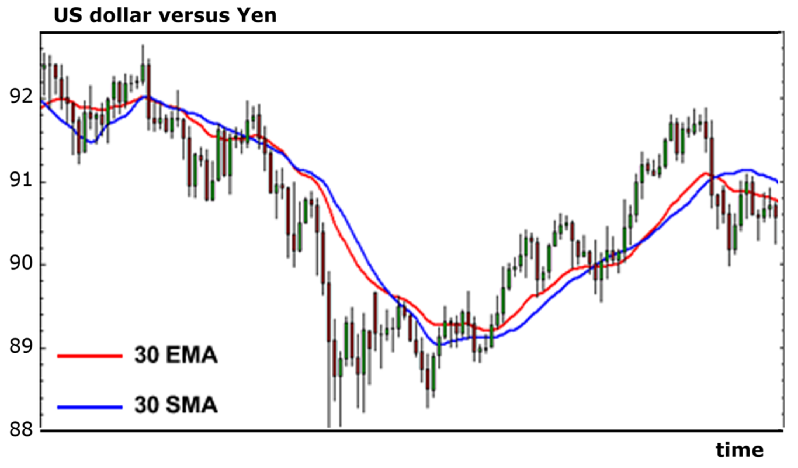
Figure 2.
This circuit implements the EMA: the capacitor Cs charges to ; when a pulse is applied to Vnext, the switch toggles to the right, during which Cs and Cint get shorted. A new voltage based on charge sharing is established, resulting in the updated VEMA.
Figure 2.
This circuit implements the EMA: the capacitor Cs charges to ; when a pulse is applied to Vnext, the switch toggles to the right, during which Cs and Cint get shorted. A new voltage based on charge sharing is established, resulting in the updated VEMA.
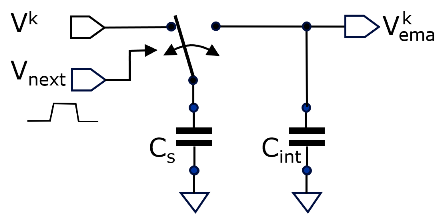
Figure 3.
The practical EMA implementation consists of generating non-overlapping clocks (f1 and f2) in response to an edge transition from Vnext, driving the gates of two NMOS transistors (left). The parasitic capacitance of the substrate diffusion diode between the two transistors forms Cs (right).
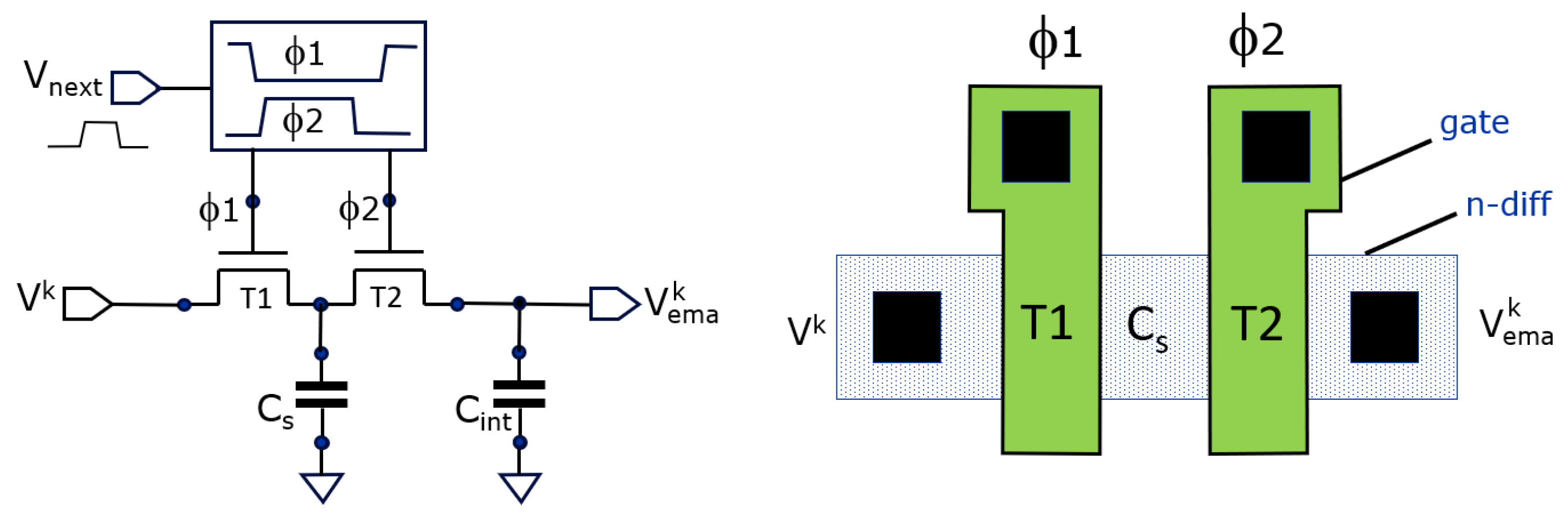
Figure 5.
An analog counter based on a switched capacitor principle useful for counting events like incident photons.
Figure 5.
An analog counter based on a switched capacitor principle useful for counting events like incident photons.
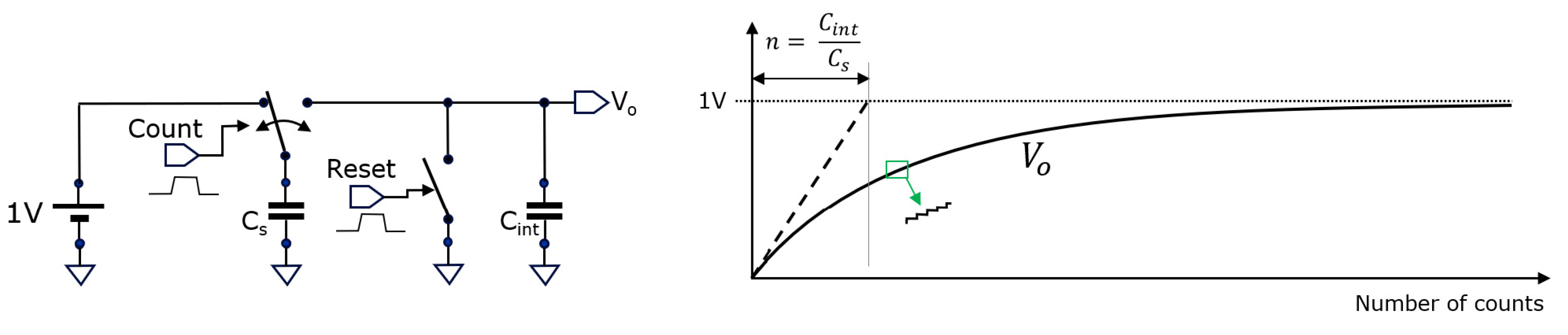
Figure 6.
The correlation functions TCOS and TSIN (left) and the schematic (right) of the two-stage averaging system for correlating the incident ToA’s of photons with these functions.
Figure 6.
The correlation functions TCOS and TSIN (left) and the schematic (right) of the two-stage averaging system for correlating the incident ToA’s of photons with these functions.
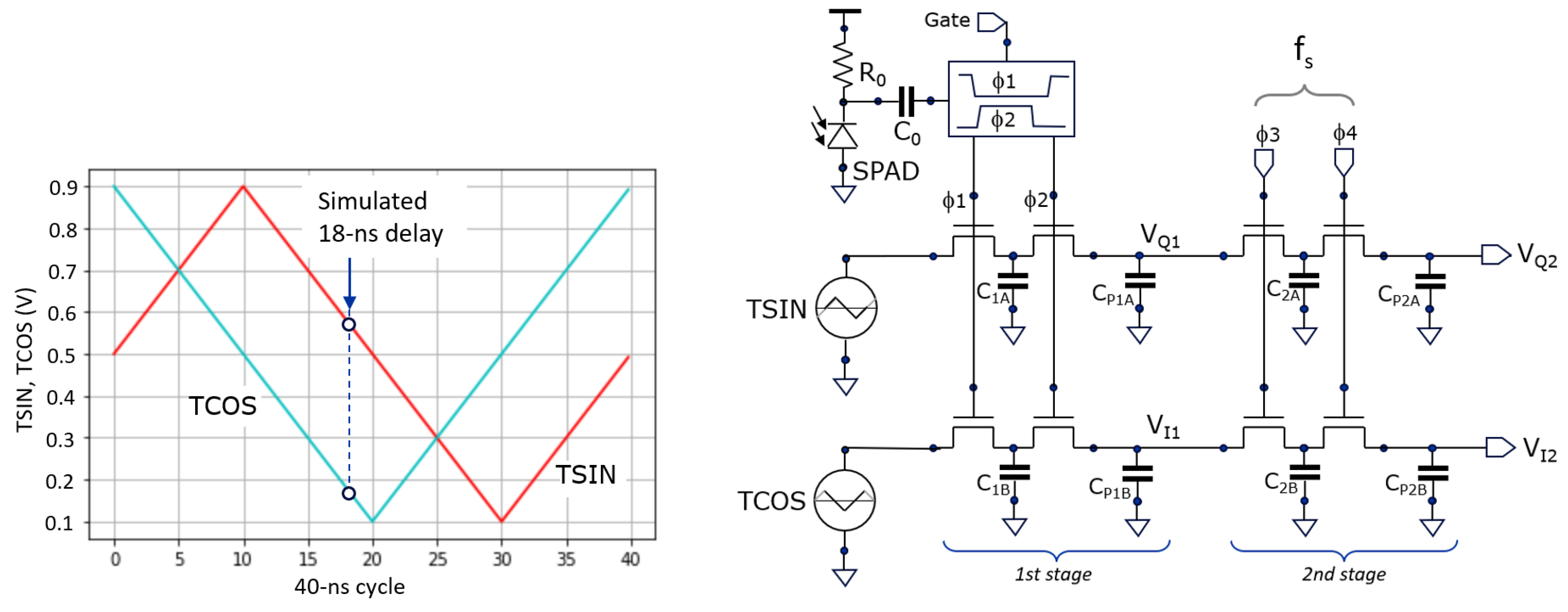
Figure 7.
Statistical simulation of a frame of 125k cycles showing the averaging of the sampled TCOS and TSIN after the first and after the second averaging stages (left). On the right, the distance is calculated based on Equations (6) and (7) and the indicated toggling frequency fs is reduced by a factor 10 after 40% of the frame.

Figure 9.
The camera is controlled by a PC over USB3 (right). An FX3 microcontroller (Infineon) provides communication with the PC through direct memory access with the image sensor chip. Left, experimental camera set-up and measured triangular waveforms generated on-chip.
Figure 9.
The camera is controlled by a PC over USB3 (right). An FX3 microcontroller (Infineon) provides communication with the PC through direct memory access with the image sensor chip. Left, experimental camera set-up and measured triangular waveforms generated on-chip.
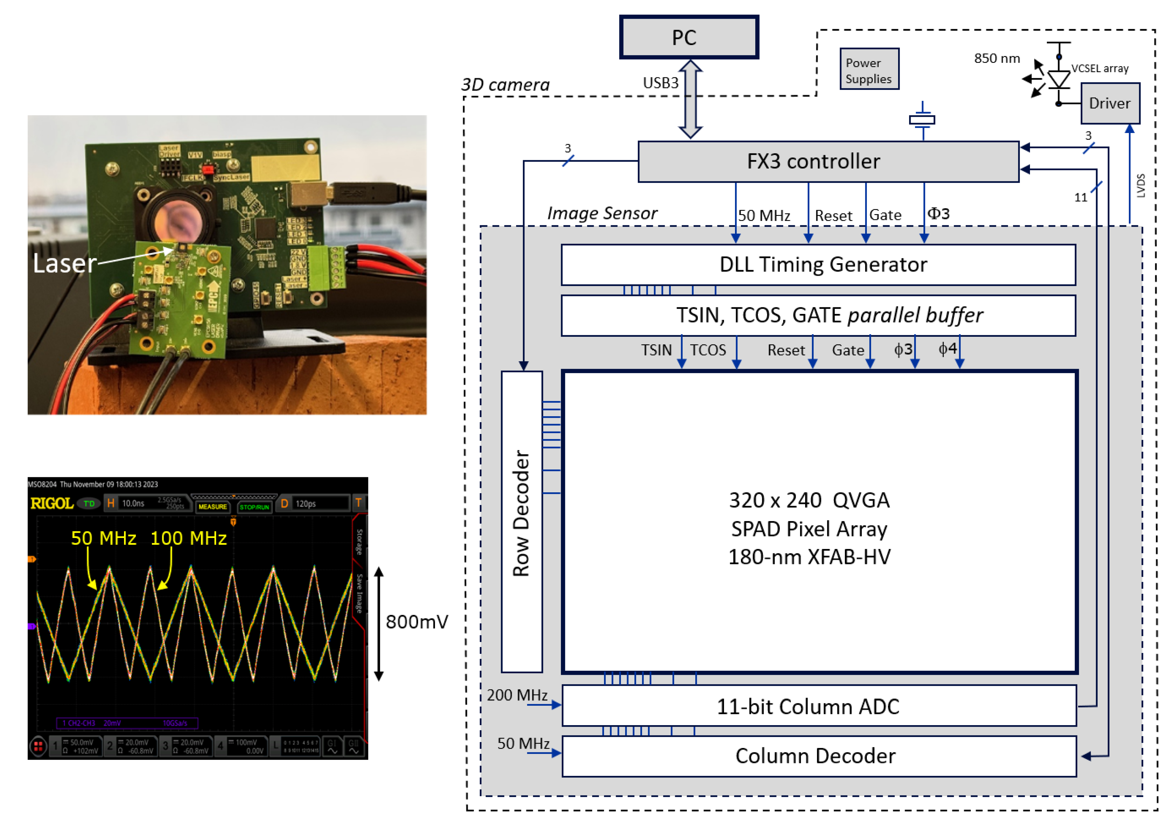
Figure 10.
Demodulation using (0°, 180°) phases at 25 MHz: Grey, Q2, I2 and 3D images. Shown right are cross-sections from the image’s row 124, giving more quantitative results, including measured and modeled depth STDV. Ambient is 1 klux at the whiteboard (b) and 2 klux at the box (e)
Figure 10.
Demodulation using (0°, 180°) phases at 25 MHz: Grey, Q2, I2 and 3D images. Shown right are cross-sections from the image’s row 124, giving more quantitative results, including measured and modeled depth STDV. Ambient is 1 klux at the whiteboard (b) and 2 klux at the box (e)
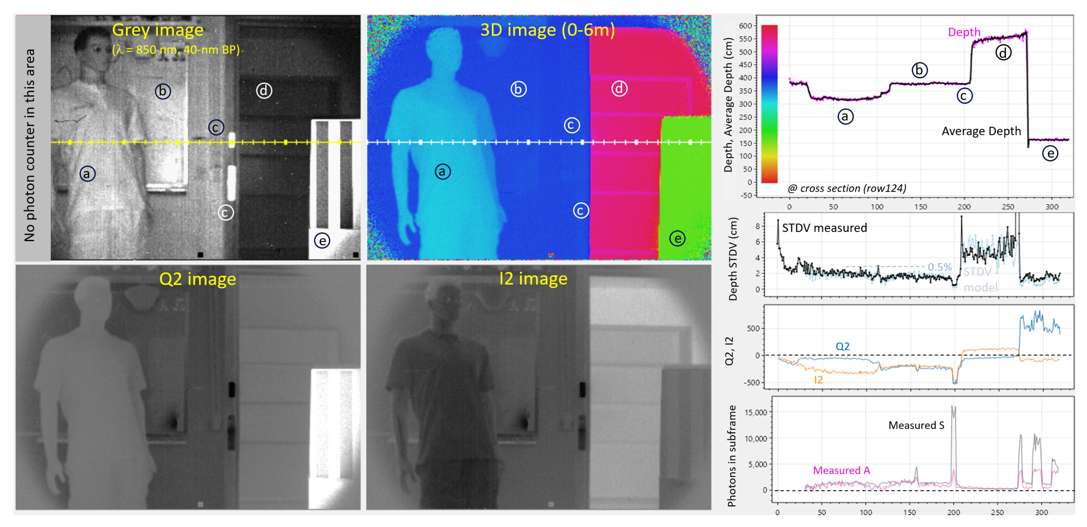
Figure 11.
Demodulation at (0°, 180°) phases at 25 MHz and (0°, 180°, 90°, 270°) phases at 100 MHz.
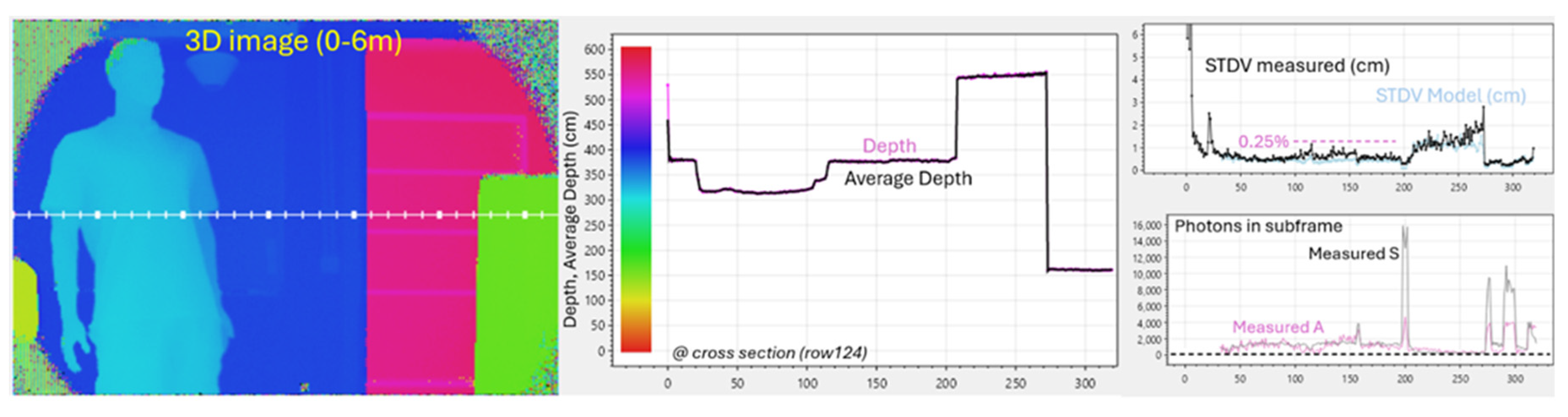
Figure 12.
Demodulation at (0°, 180°) phases at 25 MHz and (0°, 180°, 90°, 270°) phases at 100 MHz, including a spatial filter in post-processing. Same ambient as in Figure 5. Fixed pixel noise (in cm) is demonstrated on the “flat” surface of the box (e).
Figure 12.
Demodulation at (0°, 180°) phases at 25 MHz and (0°, 180°, 90°, 270°) phases at 100 MHz, including a spatial filter in post-processing. Same ambient as in Figure 5. Fixed pixel noise (in cm) is demonstrated on the “flat” surface of the box (e).
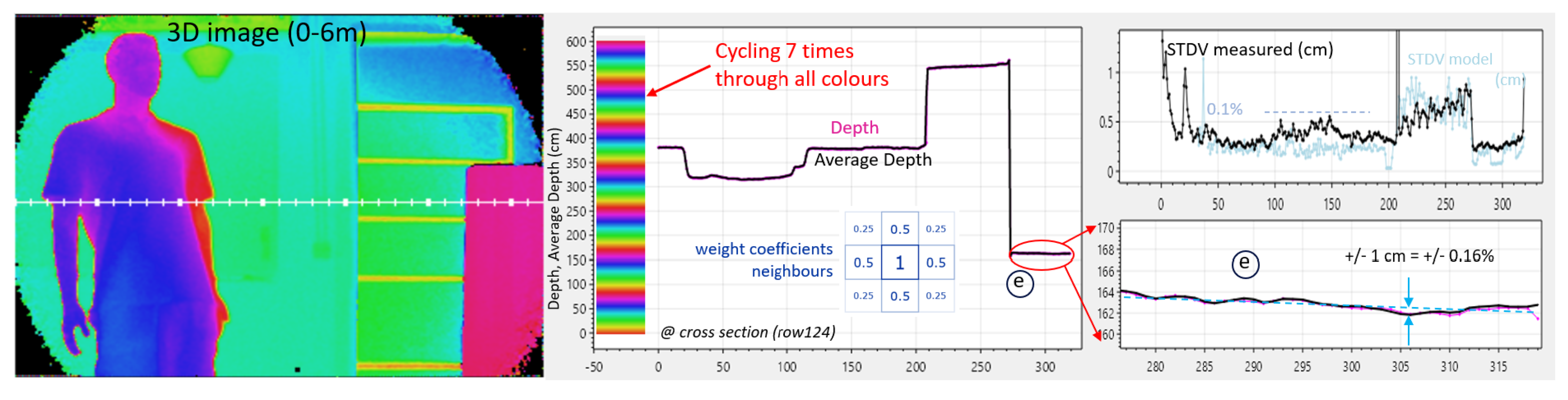
Figure 13.
Accuracy on a pixel in the center of the image. The laser is cycled over the full 360° phase range in 64 steps. The level of cyclic error is then obtained by plotting the accuracy error, being the difference between the calculated distance (derived from Q2 and I2) and the ground truth
Figure 13.
Accuracy on a pixel in the center of the image. The laser is cycled over the full 360° phase range in 64 steps. The level of cyclic error is then obtained by plotting the accuracy error, being the difference between the calculated distance (derived from Q2 and I2) and the ground truth
Disclaimer/Publisher’s Note: The statements, opinions and data contained in all publications are solely those of the individual author(s) and contributor(s) and not of MDPI and/or the editor(s). MDPI and/or the editor(s) disclaim responsibility for any injury to people or property resulting from any ideas, methods, instructions or products referred to in the content. |
© 2025 by the authors. Licensee MDPI, Basel, Switzerland. This article is an open access article distributed under the terms and conditions of the Creative Commons Attribution (CC BY) license (http://creativecommons.org/licenses/by/4.0/).
Copyright: This open access article is published under a Creative Commons CC BY 4.0 license, which permit the free download, distribution, and reuse, provided that the author and preprint are cited in any reuse.


