
Submitted:
01 October 2025
Posted:
02 October 2025
You are already at the latest version
Abstract
The General AntiParticle Spectrometer (GAPS) is a balloon-borne experiment designed to search for low-energy cosmic-ray antinuclei as a potential indirect signature of dark matter. Over the course of at least three long-duration flights over Antarctica, it will explore the sub-250 MeV/n energy range with sensitivity to antideuterons and antihelium, while also extending antiproton measurements below 100 MeV. The instrument features a tracker built from more than one thousand lithium-drifted silicon detectors, each read out by a dedicated custom integrated circuit. With the first flight scheduled for the austral summer of 2025, a new prototype chip, ANTARES4, has been developed using a commercial 65 nm complementary metal-oxide semiconductor process for use in the second flight. It integrates eight independent analog channels, each incorporating a low-noise charge-sensitive amplifier with dynamic signal compression, a CR–RC shaping stage with eight selectable peaking times, and on-chip calibration circuitry. The charge-sensitive amplifier uses metal-oxide semiconductor feedback elements with voltage-dependent capacitance to support the wide input energy range from 10 keV to 100 MeV. Four alternative feedback implementations are included to compare performance and design trade-offs. Leakage current compensation up to 200 nA per detector strip is provided by a Krummenacher current-feedback network. This paper presents the design and architecture of ANTARES4, highlighting the motivations, design drivers, and performance requirements that guided its development.
Keywords:
GAPS experiment
; spectrometer
; Si(Li) strip detectors
; readout ASIC
; charge-sensitive amplifier (CSA)
; dynamic signal compression
; Krummenacher feedback
; 65 nm CMOS technology
; balloon-borne cosmic-ray detection
; antideuteron and antihelium search
1. The GAPS Instrument
The General AntiParticle Spectrometer (GAPS) is a NASA-, INFN-, ASI-, and JAXA-funded balloon-borne experiment designed to search for low-energy cosmic-ray antiparticles as an indirect signature of dark matter [1]. Cosmological measurements indicate that non-baryonic dark matter constitutes about 27 of the total energy density of the universe, whereas baryons contribute only 5 [2]. Among indirect probes, low-energy antinuclei, particularly antideuterons, and antihelium are especially compelling because the expected astrophysical background below is strongly suppressed, enhancing the potential for discovery of new physics [3,4,5,6].
GAPS targets this low-background regime using a detection technique based on the formation and decay of exotic atoms in lithium-drifted silicon (Si(Li)) detectors. Incoming antiparticles are slowed and captured into atomic orbits, emit characteristic X-ray de-excitation lines, and then annihilate to produce charged secondaries that generate a distinctive event topology [7,8]. This approach complements magnetic-spectrometer experiments such as AMS-02 on the International Space Station and balloon missions like BESS while extending sensitivity to the lowest kinetic energies for antideuterons and improving coverage for antiprotons [9,10,11,12,13].
Figure 1 provides an overview of the GAPS instrument. The payload consists of a large-area time-of-flight (ToF) system surrounding a modular Si(Li) tracker, operated at about °C using an oscillating heat-pipe (OHP) cooling system coupled to a radiator for passive thermal control [14,15,16]. The ToF subsystem, composed of the Cube, Umbrella, and Cortina panels, provides timing information and generates the trigger for the internal Si(Li) tracker [17], while the tracker performs simultaneous X-ray spectroscopy and charged particle tracking. The electronics bay, radiator, and solar panels are also visible, highlighting the integration of the main subsystems within the payload.
The readout of the silicon-strip tracker requires low-noise, low-power front-end electronics with dynamic-range coverage from 10 to 100 . For the first flight, the readout was based on SLIDER32 (Silicon Lithium-Drifted Electronic Readout, 32 channels), an ASIC implemented in a 180 CMOS process, which enabled full-system integration and calibration [18,19,20]. For the second flight, development has shifted to the new ANTARES4 (ANTiparticle Asic REadout for Si(Li) detectors) prototype, fabricated in a 65 CMOS process. ANTARES4 targets improved noise performance, extended leakage current compensation, and reduced per-channel power consumption [21].
2. Scientific Motivations and Design Drivers
The GAPS tracker comprises more than 1000 Si(Li) detectors, each segmented into eight strips, yielding approximately 8000 readout channels [24]. During flight, the detectors operate at about °C, maintained by the OHP-based passive cooling system. Given the high channel count, the readout architecture must satisfy a strict per-channel power budget of ≤ 10 —corresponding to a total tracker power consumption of ∼ 80 —to remain compatible with the thermal design, the available battery system, and the solar array.
For the first GAPS flight, seven tracker layers are instrumented. Each layer comprises a grid of modules, with each module housing four detectors, for a total of just over 1000 Si(Li) detectors. The remaining three layers at the bottom of the tracker are equipped with mechanical dummies that act as thermal mass and emulate the power consumption of fully populated modules. Given the high channel density of the tracker, the performance of the front-end ASIC directly impacts the overall instrument capabilities. Improvements in noise, power consumption, and dynamic range propagate across thousands of channels, influencing the tracker’s data quality as well as its thermal and power budgets.
The detection strategy simultaneously measures two distinct energy regimes: low-energy X-rays from exotic-atom de-excitation in the 10–100 range and high-energy charged-particle deposits up to 100 . Accommodating both within a single readout chain demands an effective dynamic range exceeding four orders of magnitude while preserving keV-level resolution in the X-ray band. This requirement motivates the use of dynamic signal compression in the front-end, implemented via non-linear MOS feedback capacitors in the charge-sensitive amplifier (CSA) [22,23].
The main design targets for the front-end electronics are:
- Input energy dynamic range:10 to 100 .
- Energy resolution:≤5 FWHM below 100 for ∼ 40 strip capacitance.
- Noise performance: Equivalent Noise Charge (ENC) ≤ 480 e- rms at 40 .
- Power consumption:≤10/channel.
- Operating temperature: -40 °C–-35 °C.
Detector leakage current further constrains the architecture. Under nominal flight conditions at °C, Si(Li) strip leakage currents typically range from 2.5–10 [24]. However, during on-ground integration and calibration at higher temperatures (up to about °C), it can rise to hundreds of per strip. To ensure operability under these conditions, the front-end must provide leakage compensation up to at least 200 per strip.
2.1. Tracker Module Architecture
Each tracker module (Figure 2) measures roughly and integrates four lithium-drifted silicon (Si(Li)) detectors, each segmented into eight strips, for a total of 32 channels per module. The detectors are mounted within a machined aluminum frame that provides both mechanical support and a shared ground through the guard rings.
A front-end board (FEB), centrally mounted on the module, hosts the SLIDER32 readout ASIC [19], fabricated in a 180 CMOS technology, together with passive components required for biasing, calibration injection, and signal routing. The Si(Li) strips are wire-bonded directly to the ASIC inputs. The FEB also manages low-voltage power distribution, detector biasing, and control signals within the module.
Each module is enclosed between two aluminized polypropylene windows that shield the detectors from stray light and contamination. The aluminum frame includes thermal interface ports for coupling to the OHP cooling system, which maintains the detector operating temperature between °C and °C during flight.
Modules are assembled into vertical tracker rows, each comprising six aligned modules connected via custom flex-rigid printed circuit boards, as shown in Figure 3. These distribute low-voltage power, ASIC digital signals, and control lines along the row, while high-voltage bias is supplied through dedicated connectors on each module. At one end of each row, an additional flex interface board connects the modules to the tracker interface board, enabling data readout and communication with the dedicated flight computer. The rows are stacked to form multiple tracker planes, giving the GAPS tracker its modular architecture.
3. Front-End Requirements for the GAPS Tracker
The wide input energy range of the GAPS tracker, from low-energy X-rays in the 10–100 region to charged-particle deposits up to 100 , requires a front-end capable of handling over four decades of dynamic range while preserving keV-level resolution in the X-ray band. To achieve this, the ANTARES4 ASIC employs a dynamic signal compression scheme implemented in the CSA stage [22,23].
The CSA gain is determined by the feedback capacitance according to , where the effective capacitance depends on the output voltage. The technique exploits an inversion-mode MOS capacitor in the feedback path, whose capacitance varies with relative to the threshold voltage . For small signals (), the device operates in depletion, yielding a minimal feedback capacitance and therefore a high low-energy gain suitable for keV-scale X-ray resolution. For larger signals (), the device enters strong inversion, and the capacitance increases toward . As grows with the integrated charge, the corresponding gain decreases, preventing CSA saturation and enabling the measurement range up to 100 .
This architecture provides a continuous transition between two operating regimes:
- High-gain response in the X-ray range (10–100)
- Gain compression for high deposited energies, enabling measurements in the charged particle regime without saturating the front-end.
Beyond dynamic range, the design is subject to several additional constraints. Some inherited from the first-flight ASIC from the first-flight ASIC, while others reflect lessons learned from the extensive on-ground calibration carried out during instrument commissioning:
- Detector capacitance: approximately 40 per strip.
- Power budget: limited to ≤ 10 /channel, corresponding to less than 80 total for the full tracker instrument with seven active layers.
- Leakage current compensation: during flight at °C, typical leakage currents range from to 10 per strip; during on-ground calibration at higher temperatures (up to °C), the ASIC must compensate currents up to at least 200 to maintain operability.
- Integration density: one 32-channel ASIC per FEB, fully compatible with the existing module design.
- Performance metrics: low-energy gain , high-energy gain ; the compression factor quantifies the transition from the high-gain X-ray regime to the compressed charged-particle regime, with ; the kink energy, defined as the point where the linear regime transitions from low-energy X-ray detection to high-energy particle detection, is required to lie above .
4. ANTARES4 ASIC Overview
The ANTARES4 ASIC was developed as a research and development prototype using a commercial 65 CMOS process. Unlike SLIDER32, which provided a flight-qualified solution for the first GAPS mission, ANTARES4 is not intended for direct flight use. Instead, it serves as a platform to evaluate circuit topologies and design solutions to be integrated into the next-generation flight ASIC.
The transition from the 180 CMOS node of SLIDER32 to 65 was motivated by several factors. First, long-term availability of the 180 process has become uncertain, with multi-project wafer (MPW) service providers gradually discontinuing support for this technology. Second, the 65 node offers higher integration density, reduced silicon area per channel, and lower nominal supply voltage ( versus ), which together enable improved power efficiency and potentially better noise performance. Finally, adopting a modern, widely supported technology mitigates obsolescence risks and ensures the long-term sustainability of the readout electronics for future GAPS flights.
The main design objectives are as follows:
- Replace approximately 360 SLIDER32 chips in the upgraded tracker while maintaining full compatibility with the existing FEBs and mechanical module layout.
- Reduce the per-channel power consumption below 10 to comply with the strict overall tracker power budget.
- Improve noise performance and energy resolution at a nominal detector capacitance of 40 .
- Extend leakage-current compensation up to 200 per strip to guarantee operability during on-ground calibration at elevated temperatures.
Each of the eight prototype channels integrates the following building blocks:
- A low-noise CSA with a MOS-capacitor-based feedback network implementing dynamic signal compression.
- A CR–RC semi-Gaussian shaper with eight selectable peaking times to optimize the signal-to-noise ratio.
- A calibration charge-injection circuit to emulate charge deposits and evaluate the input–output channel transcharacteristic under controlled leakage-current and temperature conditions during characterization.
- A Krummenacher feedback network providing both continuous charge restoration and leakage-current compensation.
- Dedicated test outputs giving direct access to the CSA and shaper waveforms for characterization.
Figure 4 shows a simplified block diagram of a single ANTARES4 readout channel. The detector signal is DC-coupled to the input of a CSA, which integrates the collected charge on a MOS-based feedback capacitor. This element implements dynamic signal compression by providing voltage-dependent feedback capacitance. A Krummenacher network in the feedback path ensures continuous charge restoration and leakage-current compensation.
The CSA output is then processed by a CR–RC semi-Gaussian shaper with eight selectable peaking times, allowing optimization of the signal-to-noise ratio and mitigation of pile-up at the nominal event rate. A dedicated calibration charge-injection circuit is included to emulate charge deposits and evaluate the input–output channel transcharacteristic under controlled leakage-current and temperature conditions during characterization. Additionally, test outputs at both the CSA and shaper stages provide direct access to intermediate waveforms for evaluation during ASIC characterization.
4.1. Detector Leakage Current Compensation
Although nominal leakage currents for Si(Li) strips are typically 2.5–10 nA at °C, they can exceed several hundred during ground calibration near °C. Since all tracker calibration and performance validation activities are carried out on the ground, ensuring channel operability under these conditions is essential. During these procedures, the OHP-based cooling system is coupled to a cold metal plate with circulating ethanol chilled at °C, but this setup cannot maintain the nominal flight temperature of °C across the entire tracker. To address this, ANTARES4 integrates an improved Krummenacher feedback network within the CSA, designed to compensate leakage currents up to at least 200 , maximizing the number of channels that remain operational during calibration and enabling comprehensive detector characterization prior to launch.
Figure 5 summarizes the post-layout transcharacteristic of the CSA obtained at the output of the CR–RC shaper for different detector leakage currents, ranging from up to 264 . Figure 6 reports the extracted CSA gain and the equivalent feedback capacitance, illustrating the effect of dynamic compression across decades of input charge. Both simulations were performed at °C under the typical-typical (TT) process corner, with an input detector capacitance , an n-type MOS feedback capacitor, and a shaping peaking time of .
Table 1 summarizes the variation in low-energy gain, high-energy gain, compression factor, and INL (index of non-linearity, defined as the relative deviation of the measured output voltage from the ideal linear response) as a function of leakage current and input capacitance at °C. The compression factor k is defined as the ratio between the low-energy and high-energy gains, i.e., , and quantifies the strength of dynamic signal compression in the CSA. The kink corresponds to the energy where the linear regime transitions from low-energy X-ray detection to high-energy particle detection.
The simulation results show that under nominal flight conditions at °C, the low-energy gain is approximately 300 /, with an index of non-linearity below in the 10–100 X-ray region. As the leakage current increases to 214 , corresponding to on-ground calibration scenarios, the low-energy gain decreases by less than 20 , while the INL remains within . Even at 264 , which exceeds the nominal design target, the channel remains functional, with the kink energy shifting towards higher values. These results confirm that the CSA architecture supports operation under both nominal flight conditions and elevated leakage currents during system integration and calibration.
4.2. Readout Channel Layout
Figure 7 shows the complete layout of a single ANTARES4 readout channel. The design fits within the 100 channel height constraint, with a total width of 363 , and integrates the charge-injection circuit, leakage-current generator, CSA with dynamic signal compression (implemented here with the n-type MOS feedback variant), Krummenacher network, and programmable CR–RC shaper. In this configuration, the shaper output is selected for readout and routed to the corresponding ASIC pad through the analog output driver. Across the full ASIC, eight channels are implemented, four of which also include a dedicated leakage-current emulator for testing the extended-range compensation circuit during ASIC characterization.
5. Conclusions
The ANTARES4 prototype ASIC, implemented in a 65 CMOS process, has been developed as an R&D platform to evaluate circuit topologies for upgrading the GAPS Si(Li) tracker readout electronics for the second flight. The design introduces MOS-based dynamic signal compression in the CSA feedback network, extended-range leakage-current compensation, and a more compact channel layout compared to the previous SLIDER32 ASIC.
Post-layout simulation results show that the low-energy gain remains around 300 / under nominal flight conditions, with an INL below in the X-ray region and below at higher energies. The compression factor reaches about 95 under nominal leakage conditions and decreases with increasing leakage current, confirming the ability to handle input charges spanning nearly four decades. All key performance metrics, including low- and high-energy gains, compression factor, and kink energy, satisfy the design requirements.
The channel layout achieves a reduction in per-channel area of approximately 30 compared to SLIDER32, improving integration density while maintaining compatibility with the existing FEB and module footprint.
The ANTARES4 architecture scales to the full tracker channel count and is designed to replace approximately 360 SLIDER32 ASICs in the second-flight configuration. It features improved area efficiency, enhanced dynamic signal compression, and performance that fully satisfies the design requirements. Compared with the previous SLIDER32 implementation, the leakage-current compensation capability has been extended from appropriately 50 to more than 200 in the new 65 design. These advances provide a solid basis for optimizing the integration strategy and selecting the most suitable front-end design for future GAPS missions. The design has been submitted for fabrication, with full ASIC characterization planned on the fabricated prototypes.
Author Contributions
Conceptualization, L.G. and M.M.; methodology, L.G. and M.M.; software, L.G.; validation, L.G., M.M., P.L. and E.R.; formal analysis, L.G. and M.M.; investigation, L.G. and M.M.; resources, M.M.; data curation, L.G.; writing—original draft preparation, L.G.; writing—review and editing, L.G., M.M., P.L. and E.R.; visualization, L.G.; supervision, M.M.; project administration, M.M.; funding acquisition, M.M. All authors have read and agreed to the published version of the manuscript.
Funding
This work was supported in part by Istituto Nazionale di Fisica Nucleare (INFN) and in part by the Italian Space Agency (ASI) through ASI-INFN “Partecipazione italiana al GAPS - General AntiParticle Spectrometer” under Agreement no. 2018-28-HH.0.
Data Availability Statement
The raw data supporting the conclusions of this article will be made available by the authors on request.
Acknowledgments
The authors thank their colleagues in the GAPS collaboration for the many valuable discussions and insights that have helped improve this work.
Conflicts of Interest
The authors declare no conflicts of interest.
Abbreviations
The following abbreviations are used in this manuscript:
| AMS-02 | Alpha Magnetic Spectrometer-02 |
| ASIC | Application-Specific Integrated Circuit |
| ASI | Agenzia Spaziale Italiana |
| BESS | Balloon-Borne Experiment with a Superconducting Spectrometer |
| CMOS | Complementary Metal-Oxide-Semiconductor |
| CSA | Charge-Sensitive Amplifier |
| ENC | Equivalent Noise Charge |
| FEB | Front-End Board |
| FWHM | Full Width at Half Maximum |
| GAPS | General AntiParticle Spectrometer |
| INFN | Istituto Nazionale di Fisica Nucleare |
| INL | Index of Non-Linearity |
| ISS | International Space Station |
| JAXA | Japan Aerospace Exploration Agency |
| LDB | Long Duration Balloon (Facility) |
| MOSFET | Metal-Oxide-Semiconductor Field-Effect Transistor |
| NASA | National Aeronautics and Space Administration |
| OHP | Oscillating Heat Pipe |
| Si(Li) | Lithium-drifted Silicon Detector |
| ToF | Time-of-Flight |
References
- Tiberio, A.; GAPS Collaboration. Indirect Search for Dark Matter with Cosmic-Ray Antinuclei: The GAPS Experiment. J. Phys.: Conf. Ser. 2025, 3053, 012002. [Google Scholar] [CrossRef]
- Planck Collaboration. Planck 2013 Results. XVI. Cosmological Parameters. Astron. Astrophys. 2014, 571, A16. [Google Scholar] [CrossRef]
- Donato, F.; Fornengo, N.; Salati, P. Antideuterons as a Signature of Supersymmetric Dark Matter. Phys. Rev. D 2000, 62, 043003. [Google Scholar] [CrossRef]
- Baer, H.; Profumo, S. Low Energy Antideuterons: Shedding Light on Dark Matter. JCAP 2005, (12), 008. [Google Scholar] [CrossRef]
- Fornengo, N.; Maccione, L.; Vittino, A. Dark Matter Searches with Cosmic Antideuterons: Status and Perspectives. JCAP 2013, (09), 031. [Google Scholar] [CrossRef]
- Aramaki, T.; Hailey, C. J.; Boggs, S. E.; <i></i>., *!!! REPLACE !!!*; et al. Antideuteron Sensitivity for the GAPS Experiment. Astropart. Phys. 2016, 74, 6–13. [Google Scholar] [CrossRef]
- Aramaki, T.; Chan, S. K.; Craig, W. W.; <i></i>., *!!! REPLACE !!!*; et al. A Measurement of Atomic X-ray Yields in Exotic Atoms and Implications for an Antideuteron-Based Dark Matter Search. Astropart. Phys. 2013, 49, 52–62. [Google Scholar] [CrossRef]
- Mori, K.; Hailey, C. J.; Kikuchi, T.; <i></i>., *!!! REPLACE !!!*; et al. A Novel Antimatter Detector Based on X-ray Deexcitation of Exotic Atoms. Astrophys. J. 2002, 566, 604–616. [Google Scholar] [CrossRef]
- Battiston, R. The Antimatter Spectrometer (AMS-02): A Particle Physics Detector in Space. Nucl. Instrum. Methods Phys. Res., Sect. A 2008, 588, 227–234. [Google Scholar] [CrossRef]
- De Lucas, L. J. International Space Station. Acta Astronaut. 1996, 38, 613–619. [Google Scholar] [CrossRef]
- Myers, Z. D.; Seo, E. S.; Wang, J. Z.; <i></i>., *!!! REPLACE !!!*; et al. Cosmic Ray 1H and 2H Spectra from BESS 98. Adv. Space Res. 2005, 35, 151–155. [Google Scholar] [CrossRef]
- Rogers, F.; Aramaki, T.; Boezio, M.; Boggs, S. E.; Bonvicini, V.; Bridges, G.; Campana, D.; Craig, W. W.; Von Doetinchem, P.; Everson, E.; Fabris, L.; Feldman, S.; Fuke, H.; Gahbauer, F.; Gerrity, C.; Hailey, C. J.; Hayashi, T.; Kawachi, A.; Kozai, M.; <i></i>., *!!! REPLACE !!!*; et al. Sensitivity of the GAPS Experiment to Low-Energy Cosmic-Ray Antiprotons. Astropart. Phys. 2023, 145, 102791. [Google Scholar] [CrossRef]
- Saffold, N.; Aramaki, T.; Bird, R.; <i></i>., *!!! REPLACE !!!*; et al. Cosmic Antihelium-3 Nuclei Sensitivity of the GAPS Experiment. Astropart. Phys. 2021, 130, 102580. [Google Scholar] [CrossRef]
- Okazaki, S.; Fuke, H.; Ogawa, H. Development of Meter-Scale O-Shaped and U-Shaped Oscillating Heat Pipes for GAPS. In Proceedings of the 2014 IEEE Aerospace Conference, Big Sky, MT, USA, 1–8 March 2014 (8 March 2014). [Google Scholar] [CrossRef]
- Okazaki, S.; Fuke, H.; Ogawa, H. Performance of Circular Oscillating Heat Pipe for Highly Adaptable Heat Transfer Layout. Appl. Therm. Eng. 2021, 198, 117497. [Google Scholar] [CrossRef]
- Fuke, H.; Okazaki, S.; Kawachi, A.; <i></i>., *!!! REPLACE !!!*; et al. Design and Application of Multi-Loop Capillary Heat Pipes to Cool GAPS Silicon Detectors. Nucl. Instrum. Methods Phys. Res., Sect. A 2023, 1049, 168102. [Google Scholar] [CrossRef]
- Feldman, S. N.; Aramaki, T.; Boezio, M.; <i></i>., *!!! REPLACE !!!*; et al. The GAPS Time-of-Flight Detector. PoS(ICRC2023) 2024, 444, 120. [Google Scholar]
- Riceputi, E.; Manghisoni, M.; Re, V.; Ghislotti, L.; Lazzaroni, P.; Boezio, M.; Fabris, L.; Zampa, G. Experimental Results from the Characterization of a 32-Channels Mixed-Signal Processor for the GAPS Experiment. In 2023 IEEE Nuclear Science Symposium and Medical Imaging Conference (NSS/MIC); IEEE: Vancouver, BC, Canada, 2023. [Google Scholar]
- Manghisoni, M.; Ghislotti, L.; Lazzaroni, P.; Re, V.; Riceputi, E.; Ratti, L.; Fabris, L.; Boezio, M.; Zampa, G. A 32-Channels Readout ASIC for X-ray Spectrometry and Tracking in the GAPS Experiment. IEEE Trans. Nucl. Sci. 1033. [Google Scholar]
- Ghislotti, L.; Boezio, M.; Fabris, L.; Lazzaroni, P.; Manghisoni, M.; Ratti, L.; Re, V.; Riceputi, E.; Zampa, G. Energy Threshold Calibration of the GAPS Experiment Si(Li) Tracker Readout Electronics. Il Nuovo Cimento C 2024, 47, 1–5. [Google Scholar] [CrossRef]
- Ghislotti, L.; Lazzaroni, P.; Manghisoni, M.; Riceputi, E. Low-Noise Wide Dynamic Range Charge Sensitive Amplifier in 65 nm CMOS Technology for the Second Flight of the GAPS Experiment. In Proceedings of the 2024 19th Conference on Ph.D. Research in Microelectronics and Electronics (PRIME); 2024; pp. 1–4. [Google Scholar] [CrossRef]
- Manghisoni, M.; Comotti, D.; Gaioni, L.; Ratti, L.; Re, V. Dynamic Compression of the Signal in a Charge Sensitive Amplifier: From Concept to Design. IEEE Trans. Nucl. Sci. 2015, 62, 2318–2326. [Google Scholar] [CrossRef]
- Manghisoni, M.; Comotti, D.; Gaioni, L.; Ratti, L.; Re, V. Dynamic Compression of the Signal in a Charge Sensitive Amplifier: Experimental Results. IEEE Trans. Nucl. Sci. 2018, 65, 636–644. [Google Scholar] [CrossRef]
- Xiao, M.; Stoessl, A.; Roach, B.; Gerrity, C.; Bouche, I.; Bridges, G.; von Doetinchem, P.; Hailey, C.J.; Kraych, D.; Katt, A.; Law, M.; Lowell, A.; Martinez, E.; Perez, K.; Reed, M.; Rodriguez, C.; Saffold, N.; Stringfield, C.; Weiner, H.; Yee, K. Large-Scale Detector Testing for the GAPS Si(Li) Tracker. IEEE Transactions on Nuclear Science 2023, 70, 2125–2133. [Google Scholar] [CrossRef]
Figure 1.
Schematic overview and photograph of the GAPS instrument. Left: Rendering of the science payload highlighting the main subsystems, including the Si(Li) tracker enclosed within the ToF Cube, the ToF Umbrella and Cortina panels, the radiator, the electronics bay, and the solar panels. Right: The flight-ready GAPS instrument integrated at the NASA Long Duration Balloon (LDB) facility at McMurdo Station, Antarctica, during the commissioning campaign.
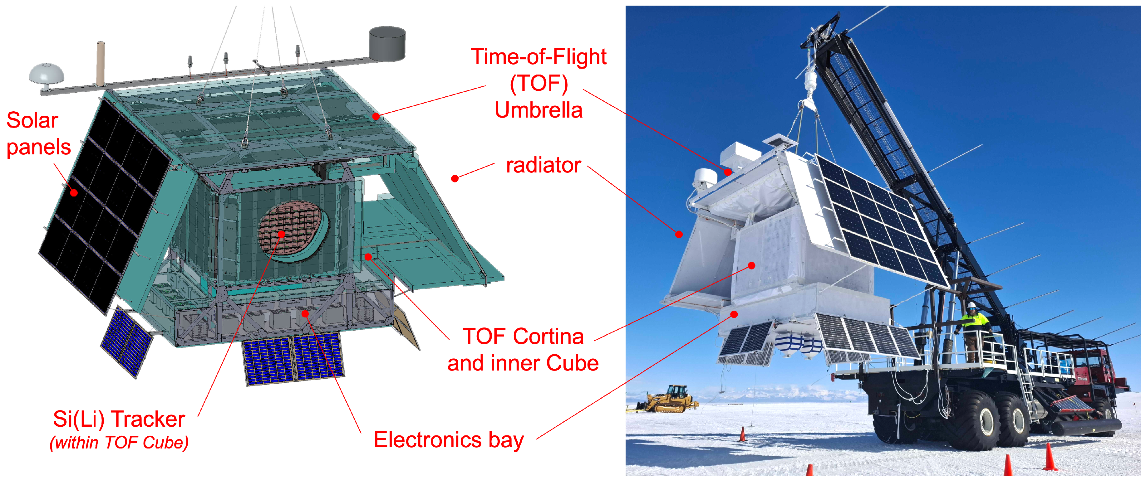
Figure 2.
Layout of a GAPS tracker module [19]. Four Si(Li) detectors are mounted in an aluminum frame and connected to a central FEB hosting the 32-channel readout ASIC. The FEB provides high-voltage bias distribution, low-voltage supply and digital control, as well as detector readout via the ASIC. Thermal coupling to the OHP cooling system occurs through the aluminum frame.
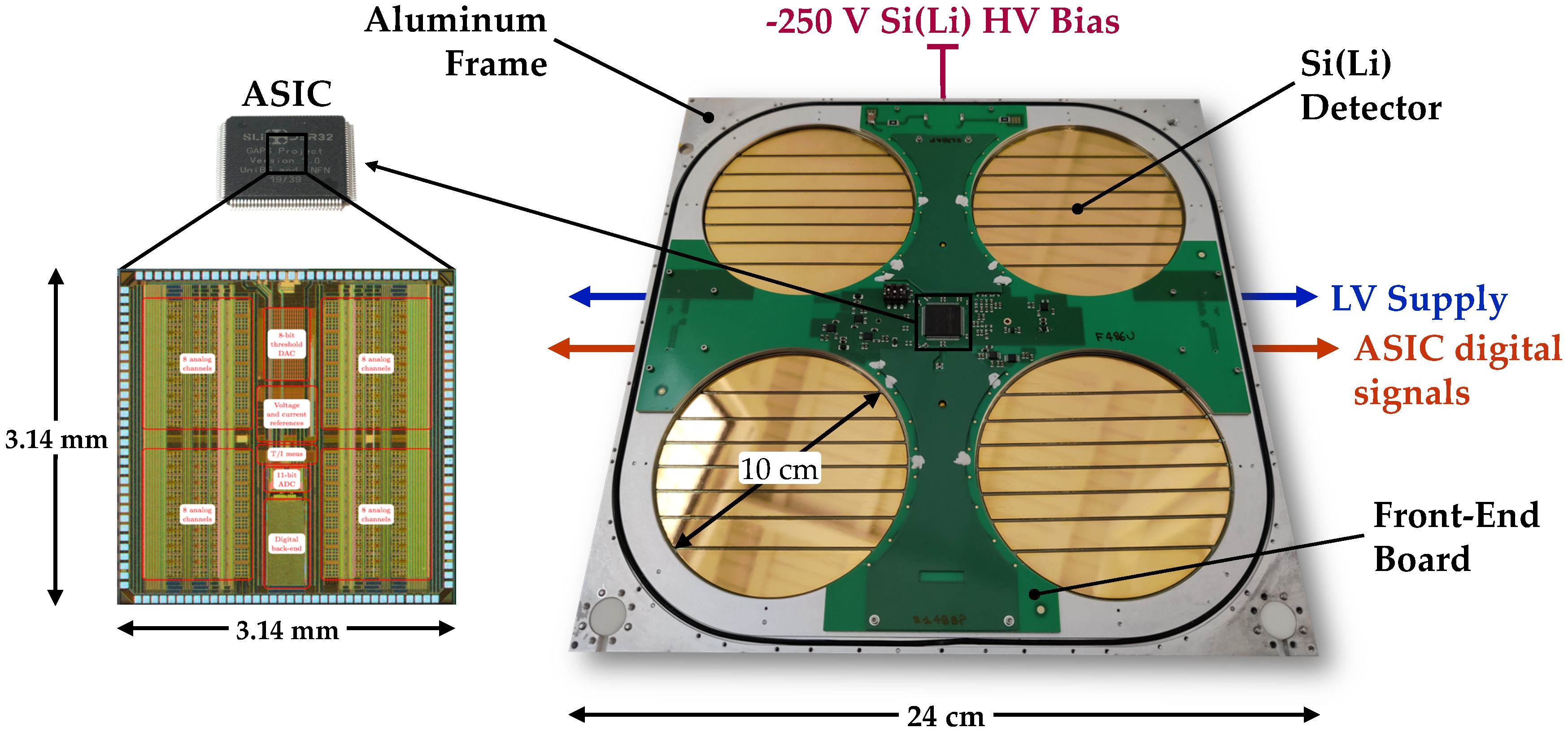
Figure 3.
Schematic of a tracker row comprising six modules connected in series. Low-voltage power, ASIC digital signals, and control lines are distributed along the row via a custom flex-rigid printed circuit board. An additional flex interface board connects the module row to the interface board, enabling data readout and communication with the dedicated flight computer.
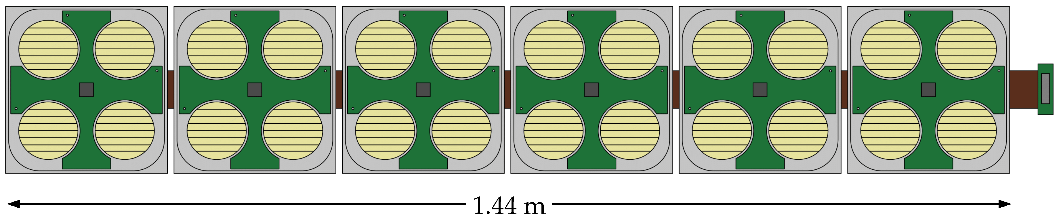
Figure 4.
Simplified block diagram of a single ANTARES4 readout channel, showing the CSA with the MOS-based feedback capacitance , CR–RC shaper, calibration injection circuit, and Krummenacher leakage-current compensation feedback with transconductance .
Figure 4.
Simplified block diagram of a single ANTARES4 readout channel, showing the CSA with the MOS-based feedback capacitance , CR–RC shaper, calibration injection circuit, and Krummenacher leakage-current compensation feedback with transconductance .
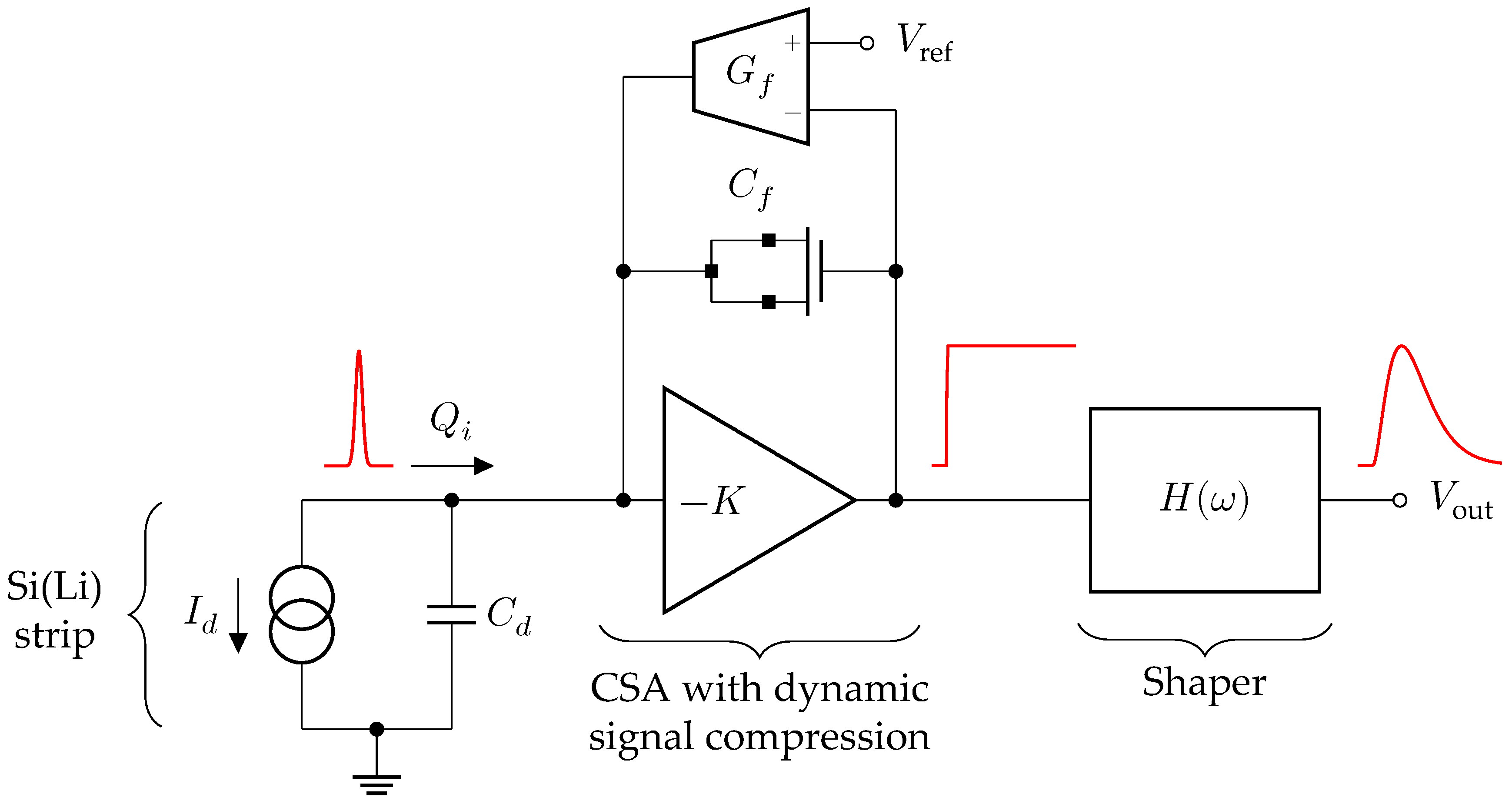
Figure 5.
Channel transcharacteristic at the output of the CR–RC shaper for different leakage currents, illustrating the impact of detector leakage on dynamic signal compression in ANTARES4. Post-layout simulations were performed at °C under the typical-typical (TT) process corner, with an input detector capacitance , an n-type MOS feedback capacitor, and a peaking time . The curves are shown for leakage currents ranging from up to 264.
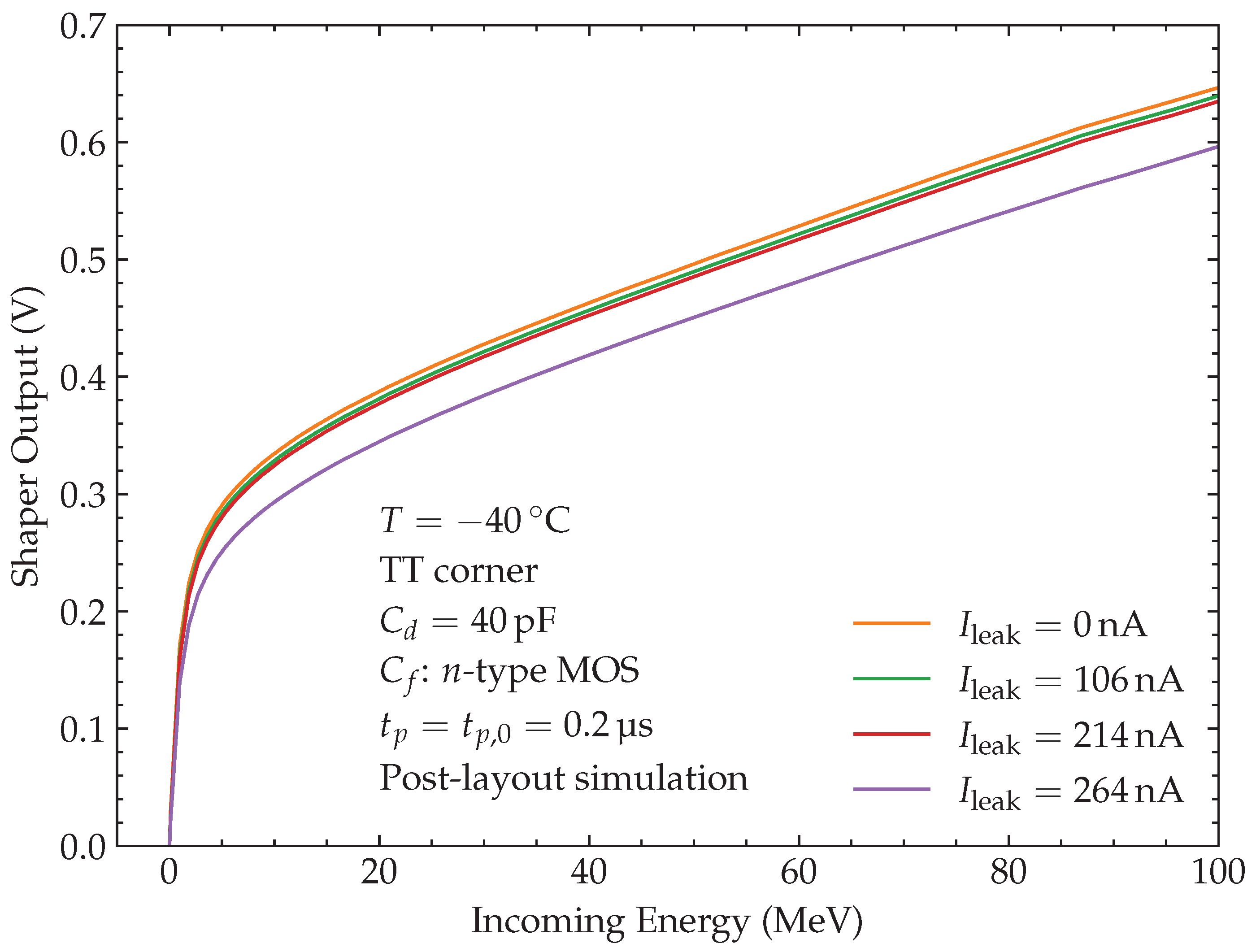
Figure 6.
Channel transcharacteristic analysis at zero leakage current, showing the extracted gain and equivalent feedback capacitance as a function of input energy. Simulations were carried out at °C under the typical-typical (TT) process corner, with , an n-type MOS feedback capacitor, and a peaking time . The simulation results highlight the effective compression behavior of the CSA for .

Figure 7.
Layout of a single ANTARES4 readout channel, showing the charge-injection circuit, leakage-current generator, CSA with dynamic signal compression (implemented here with the n-type MOS feedback variant), Krummenacher network, and programmable CR–RC shaper with eight selectable peaking times. The shaper output is routed to the corresponding ASIC pad through the analog output driver. The layout fits within the 100 channel height constraint, with a total width of 363.
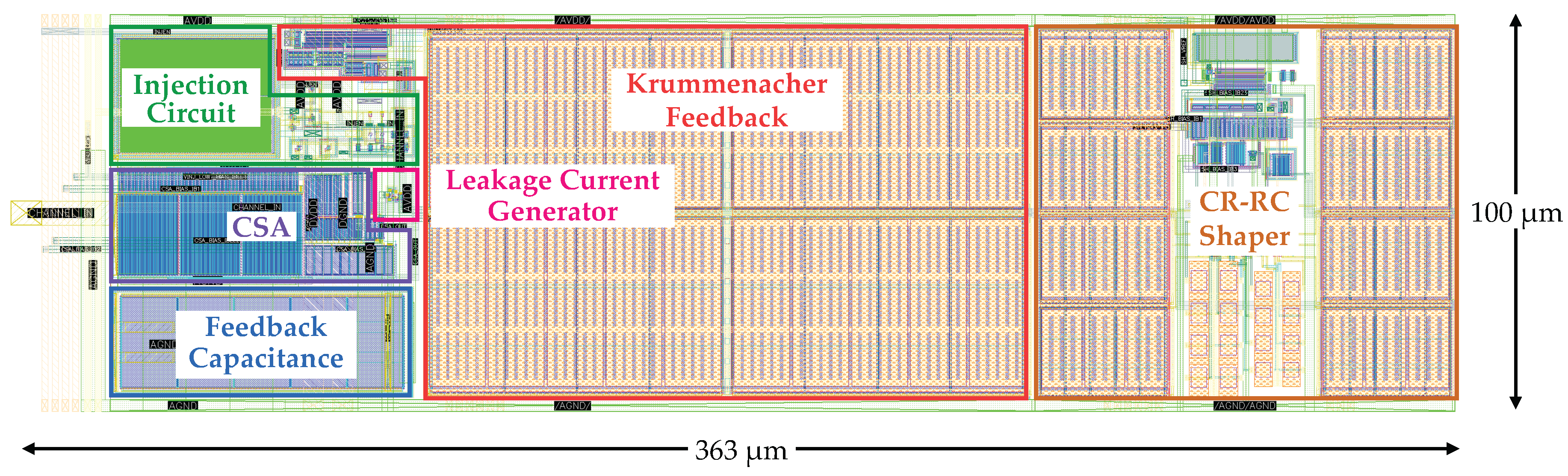

Table 1.
Linearity, gain, and compression factor versus detector leakage current at °C for a representative channel. and denote low- and high-energy gains, respectively; and are the indices of non-linearity in the low- and high-energy regions. The compression factor quantifies the transition from the high-gain X-ray regime to the compressed charged particle regime. The kink corresponds to the energy where the linear regime transitions from low-energy X-ray detection to high-energy particle detection.
| k | Kink | ||||||
|---|---|---|---|---|---|---|---|
| () | () | () | () | () | () | – | () |
| 0 | 0 | 305 | 0.31 | 3.21 | 1.78 | 95 | 1104 |
| 0 | 40 | 300 | 0.44 | 3.17 | 2.02 | 94 | 1129 |
| 106 | 40 | 268 | 0.49 | 3.16 | 1.93 | 84 | 1246 |
| 214 | 40 | 251 | 0.57 | 3.15 | 1.90 | 79 | 1312 |
| 264 | 40 | 208 | 0.39 | 3.05 | 2.07 | 68 | 1439 |
Disclaimer/Publisher’s Note: The statements, opinions and data contained in all publications are solely those of the individual author(s) and contributor(s) and not of MDPI and/or the editor(s). MDPI and/or the editor(s) disclaim responsibility for any injury to people or property resulting from any ideas, methods, instructions or products referred to in the content. |
© 2025 by the authors. Licensee MDPI, Basel, Switzerland. This article is an open access article distributed under the terms and conditions of the Creative Commons Attribution (CC BY) license (http://creativecommons.org/licenses/by/4.0/).
Copyright: This open access article is published under a Creative Commons CC BY 4.0 license, which permit the free download, distribution, and reuse, provided that the author and preprint are cited in any reuse.


