
Submitted:
01 September 2025
Posted:
03 September 2025
You are already at the latest version
Abstract
ZnO thin films were deposited on soda-lime glass substrates using the chemical spray pyrolysis method at a temperature of 500 ºC. After deposition, the substrate was irradiated with H+ and Ar+ ions using a 10 keV energy with a Colutron ion gun. We investigated the optical, structural, and morphological properties resulting from ion irradiation through Rutherford Backscattering Spectrometry, Ultraviolet and Visible Spectroscopy, X-ray diffraction, and Scanning Electron Microscopy. We observed a decrease in the optical band gap in the irradiated samples, attributed to the quantum confinement effect resulting from changes in the crystallite size. The diffractograms revealed diffraction peaks corresponding to the planes characteristic of the hexagonal wurtzite phase of ZnO, which indicate that the films are polycrystalline with a preferential orientation along the c-axis. We observed a decrease in the average crystallite size in the samples after ion irradiation. The morphological study reveals an increase in the average particle size after irradiation, and a change in their shape, from spherical in the pristine sample to flake-like in the irradiated samples. The sample irradiated with Ar+ ions also exhibited a bimodal distribution in particle size, which is attributed to the defects and nucleation centers created during the irradiation process.
Keywords:
zinc oxide
; chemical spray pyrolysis
; ion irradiation
; thin films
1. Introduction
Ion irradiation is a technique used in materials science to control the physical properties of a material. This process involves bombarding the material's surface with a beam of ions, triggering a series of physical interactions at the atomic level that can induce structural, morphological, optical, electrical, and mechanical changes.
When the ions penetrate the material, they transfer their energy to the atoms in the crystal lattice through elastic and inelastic collisions. This process can generate point defects, vacancies, interstitial defects, and localized amorphization, leading to modifications in the crystal structure. The density of these defects depends on the type of ion, its energy, the applied fluence, and the nature of the target material [1].
The irradiation using different types of ions has found applications in fields such as microelectronics, nanotechnology, and surface modification. However, its most important role is in the development of advanced functional materials. With its precision and versatility, ion irradiation has not only established itself as a powerful tool for materials engineering at the nanoscale but also opened up new possibilities for material design and functionality, inspiring the future of materials science [2].
Zinc oxide (ZnO) is an inorganic compound with unique properties that has been studied for industrial, medical, and technological applications [3]. ZnO is an n-type semiconductor, with a wide direct bandgap of 3.37 eV and a high exciton energy of 60 meV, which commonly crystallizes in a hexagonal structure known as wurtzite. In this way, ZnO is an ideal material for the development of various devices, including gas sensors, light-emitting diodes (LEDs), thin-film transistors (TFTs), and solar cells [4,5,6,7].
Spray pyrolysis is a highly effective and versatile method for synthesizing zinc oxide thin films, enabling the precise control of their optoelectronic properties. This technique begins with the generation of a fine aerosol using an ultrasonic atomizer that creates a mist of precursor solution. A stream of gas then carries the aerosol to a deposition chamber, where thermal pyrolysis takes place on a preheated substrate. This heating process promotes the decomposition of the precursor material, leading to the formation and deposition of homogeneous, compact, and uniform ZnO thin films on the substrate surface. One of the primary advantages of spray pyrolysis is its cost-effectiveness, making it accessible for both research and industrial applications. The process operates at atmospheric pressure, which simplifies equipment requirements and enhances safety. Additionally, it can be performed at relatively low temperatures, thereby reducing energy consumption and enabling the use of temperature-sensitive substrates. Furthermore, spray pyrolysis is capable of efficiently covering large surface areas, making it suitable for various applications in electronics, optics, and sensors. This method provides a promising pathway for the scalable production of high-quality ZnO thin films tailored for specific optoelectronic applications [8,9].
Various techniques exist for depositing ZnO thin films, but achieving the desired properties for specific applications can be challenging. One method of modifying the material is through thermal treatments; however, this approach does not allow for control over the size of the synthesized particles. A more promising alternative is ion irradiation, which enables the manipulation of material properties by varying irradiation parameters such as energy, fluence, ion mass, and implantation angle. The irradiation of ZnO with ions of different energies and fluences is a controlled process typically performed at room temperature. Using accelerators, the energy and fluence can be precisely tuned to generate specific defects in ZnO, thereby predictably modifying its physical properties.
Ion irradiation induces point defects, including Zn and O vacancies, as well as interstitials. For instance, Sarkar et al. [10] observed clusters of Zn and O vacancies after irradiating ZnO with 1.2 MeV Ar+ and 800 keV O+ ions. They also noticed that the band-edge photoemission intensity decreases with increasing ion fluence. In contrast, emission at 2.4 eV (associated with oxygen vacancies) increases more with Ar+ ions than with O+ ions. Dee et al. [11] reported that ZnO nanowires converted from a crystalline wurtzite structure to a disordered amorphous state after irradiation with 70 keV H+ at 2×10¹⁷ ions/cm-2. Studies on nanosized ZnO also reveal lattice rearrangement. Wu et al. [12] observed that upon irradiation of nanorods with 180 keV H+ ions, the lattice constant c contracts, and the crystallinity improves slightly, suggesting that electronic and thermal shock waves induce compressive stresses that rearrange the lattice. They also found a blue shift in the excitonic emission of ZnO nanorods after irradiation with H+ at 180 keV, which is also attributed to compressive stresses that increase the band gap.
This study investigated the deposition of ZnO thin films on soda-lime glass using the spray pyrolysis technique at a temperature of 500 ºC. Afterward, the samples were implanted with 10 keV H+ and Ar+ ions at room temperature using a Colutron ion gun, with a fluence of 1×10¹⁴ ions/cm². Subsequently, variations in the structural, morphological, and optical properties of the films were examined.
2. Materials and Methods
Zinc oxide (ZnO) thin films were synthesized on a borosilicate glass substrate using the ultrasonic spray pyrolysis technique [13]. The precursor solution was prepared by dissolving 10.97 g of zinc acetate in 250 ml of deionized water at 40 °C. To stabilize the solution and achieve complete dissolution of the salts, 50 ml of acetic acid was added to the solution, followed by 700 ml of methanol. Of this solution, 50 ml was atomized onto the substrate, which was heated to 500°C. Once the samples were obtained, one substrate was left pristine, while others were irradiated with H+ and Ar+ ions using a 10 keV energy with a Colutron-type ion gun model at the Science Faculty, UNAM. ZnO thin films were irradiated with H+ and Ar+ ions at an energy of 10 keV and a fluence of 2×10¹⁴ ions/cm2. The samples were analyzed both before and after irradiation to investigate the changes in the semiconductor's structural, optical, and morphological properties. The structural properties of the films were analyzed using X-ray diffraction (XRD) with Cu Kα radiation on a Bruker D8 Advance diffractometer. The morphology and variations in particle size of the ZnO films were examined using Scanning Electron Microscopy (SEM) with a FEG JEOL JSM-7800 microscope. Additionally, the optical properties of the ZnO films were measured at room temperature using an Agilent HP 8453 UV-Vis spectrophotometer, which covers a spectral range of 300-1100 nm.
3. Results and Discussion
3.1. RBS Results
Once the ZnO film was deposited on the Borosilicate glass substrate, we determined the film thickness using the Rutherford Backscattering Spectrometry (RBS) technique. The measurement was performed using the 3 MV Pelletron-type accelerator (NEC 9SDH-2) at the Physics Institute of the National Autonomous University of Mexico (UNAM), with a 2.5 MeV alpha beam used as the projectile. Alpha particles collide with the sample and scatter at an angle of 167º before being detected by a surface barrier detector. A multichannel analyzer processes the analog signals produced by the system to create the Rutherford Backscattering spectrum. In this spectrum, the target element is identified by the energy of the backscattered particles resulting from specific reactions between the incident ions and the target element. Figure 1 displays the RBS spectrum of the ZnO thin film, highlighting the elements that compose the material.
To calculate the thickness of the thin film, the FWHM of the Zn peak and the energy loss values of the alpha particles interacting with the Zn atoms were used. These values were obtained using the SRIM code [14]. When conducting an RBS experiment, alpha particles lose energy in various ways depending on the type of atom they collide with and the depth at which the atom is located. By calculating the stopping power of the alpha particles for each element in the material, we can determine the thickness of the film using the following equation [15]:
In this equation, X denotes the thickness of the zinc layer, ΔE represents the energy lost by alpha particles during their interaction with zinc atoms, and [ε] indicates the stopping power of the alpha particles in zinc. The stopping power is a crucial parameter in determining the thickness of the zinc film, and reflects how effectively the material absorbs the energy of the incoming alpha particles. As alpha particles penetrate the zinc layer, their energy diminishes due to interactions such as ionization and scattering. According to Equation (1), the thickness of the ZnO thin film is measured to be 93 ± 5 nm.
3.2. SRIM Simulations
The SRIM (Stopping and Range of Ions in Matter) code utilizes the Monte Carlo method to investigate how particles interact with matter [14]. This approach relies on probabilistic processes, generating random numbers and running multiple simulations to explore various scenarios. By considering initial conditions, such as the type of projectile, its energy, angle of incidence, and the elemental composition of the material, SRIM can simulate the different processes that occur during the interaction between the projectile and the material. It provides reliable outputs, including the depth profile of implanted ions, the distribution of damage (vacancies per ion), energy loss profiles, and ionization processes.
Electron stopping power (Se) and nuclear stopping power (Sn) are the two fundamental mechanisms through which charged ions dissipate energy as they penetrate a solid material. These processes influence not only the depth of ion penetration but also the modifications of structural damage inflicted and the subsequent alterations to the physical properties of the irradiated materials. Electronic stopping power occurs when the incoming ion transfers energy to the electrons in the target material. This interaction with the electron cloud triggers a cascade of excitations and ionizations, which can potentially lead to the formation of electronic defects. In some instances, these processes may result in significant modifications in the material's optical characteristics or electrical conductivity [16].
On the other hand, nuclear stopping power results from elastic collisions between the ion and the nuclei of the target material. These energetic interactions induce atomic displacements within the crystal lattice, creating defects such as vacancies and interstitials, as well as cascading damage. The direct energy transfer between the ion and the target nucleus generates structural disorder, which may lead to a reduction in crystallite size or even lead to the amorphization of the material. Through these interactions, the material's microstructure undergoes profound changes, influencing its overall performance and durability [17].
As previously discussed, when incident ions traverse a material, they collide with the atoms in the matrix, resulting in a gradual loss of their energy. This energy transfer continues until the ions come to a stop within the material. As they collide, the recoiling atoms gain enough energy to induce further recoils, creating a dynamic cascade of collisions. These interactions can lead to either the ionization or excitation of surrounding atoms, leaving a trail of energized atoms in the ion's path. Consequently, the temperature within this localized region increases rapidly, creating a narrow cylindrical zone known as a columnar defect or ion track. The intense transfer of energy results in the swift melting of the target material, generating a thermal spike that significantly raises the local temperature. This localized increase in temperature during irradiation has the potential to anneal the material's defects [12,18,19].
Figure 2 presents a comparison of the SRIM simulation results for (a) the concentration of H and Ar atoms in the ZnO thin film, (b) the electronic energy loss (ionization events) of H and Ar as they interact with the electrons of the atoms in the ZnO film, and (c) the nuclear energy loss (resulting in vacancies and defects) due to the interaction of H and Ar with the nuclei of the atoms comprising the film and the matrix. The vertical red line in the three figures indicates the boundary between the film (on the left side) and the substrate (on the right side). These results were obtained with the SRIM code using the following data: a 93±5 nm ZnO film deposited on a borosilicate glass matrix and irradiated with H+ and Ar+ ions at an energy of 10 keV and a fluence of 2×10¹⁴ ions/cm2.
Figure 2(a) depicts the distribution of H (blue curve) and Ar (green curve) ions when they interact with the material composed of a 93±5 nm ZnO layer and a glass borosilicate substrate. The distinct values of electronic and nuclear energy loss for H+ and Ar+ ions lead to their different behavior. It's fascinating to observe that some H+ ions remain implanted in the film when they interact with Zn or O atoms, while the rest pass through the ZnO and stop in the substrate. In the case of Ar ion interaction with the material, the scene is different. Due to their higher mass, Ar ions lose more energy when interacting with the elements that compose the film and come to a complete stop within it at 300 Å. On the other hand, the H+ ions pass through the film and stop inside the substrate at 2200 Å. The implications of these stopping points are significant, as they can influence the performance of materials in various applications.
Figure 2(b) illustrates the ionization events resulting from the electronic energy loss of H+ and Ar+ ions as they interact with the atoms that form the films and the substrate. The SRIM simulation indicates that the elements forming the ZnO film become highly ionized when irradiated with Ar+ ions. In this case, ionization of the atoms forming the film is high at the surface and declines sharply at 200 Å, reaching nearly zero by 270 Å. On the other hand, the electronic energy loss of H+ ions is distributed almost uniformly throughout the ZnO film, continuing the ionization process inside the substrate.
Figure 2(c) shows the defects created during irradiation with H+ and Ar+. The number of vacancies produced during Ar+ irradiation ranges from the surface to 270 Å and is significantly higher than that produced during H+ irradiation.
3.3. Optical Properties
Figure 3 presents the transmittance measurements for a pristine ZnO sample as well as samples irradiated with H⁺ and Ar⁺ ions, covering the wavelength range of 300 to 1100 nm. The spectra reveal a decrease in transmittance in the UV region, particularly between 360 and 380 nm, which can be attributed to fundamental bandgap absorption. However, beyond 370 nm, the transmittance increases to between 80% and 95% in the visible range. The unirradiated sample exhibits the highest transmittance value with 95%. In contrast, the irradiated samples show a reduction in transmittance within the visible range, especially the Ar-irradiated material, which has a transmittance of 81%. The same behavior has been observed by Sarkar et al [10]. They attribute it to new defect levels that absorb light or to the increase in scattering due to changes in grain size, which results from ionization effects and defects created during irradiation. This observation also aligns with our SRIM simulations presented in Figure 2(a) and Figure 2(b).
Based on the transmittance results of Figure 3 and the Tauc relationship (Equation (2)), we can calculate the optical band gap value of the semiconductor [20].
In Equation (2), α represents the absorption coefficient, hv denotes the photon energy, Eg is the optical band gap, and A refers to a constant related to the material's refractive index.
The absorption coefficient is determined using the following equation, which connects transmittance (T) and sample thickness (x). The last variable was obtained through the RBS technique as outlined in Equation (1).
The optical band gap of the material can be determined by plotting (αhν)2 against the energy of the incident radiation. The optical band gap energy is defined as the point at which the linear portion of the curve intersects the energy axis [21].
The results presented in Table 1 indicate that ion irradiation leads to a slight decrease in the optical band gap, and this effect is directly related to the mass of the irradiated ion [22]. We propose that this decrease is attributed to the quantum confinement effect, which arises from changes in the crystallite size after irradiation, and is consistent with the findings in Table 2. This phenomenon can be linked to the generation of a cascade of collisions, as well as excitation or ionization events, which introduce defects within the band gap. As illustrated in Figure 2, the defects that cause the reduction in the band gap are primarily a result of ionization events (electronic energy loss) when exposed to H+ ions. On the other hand, when materials are subjected to irradiation with Ar+ ions, the reduction in the band gap primarily results from the creation of vacancies and defects due to the energy loss linked to nuclear interactions. This ion bombardment not only changes the lattice parameters of the films but also initiates a significant process of strain relaxation within the crystalline structure. These modifications to the crystalline lattice result in changes to the material's electronic properties, which are evident as a marked decrease in the energy band gap. Research conducted by Abdel-Galil et al. [23], Soubhik et al. [24], Singh et al. [25], and Khawal et al. [26] supports these findings, demonstrating that the band gap consistently decreases with ion irradiation, regardless of the mass of the ion used.
3.4. Structural Properties
The crystalline structure of the ZnO thin films was thoroughly analyzed using X-ray diffraction (XRD), as illustrated in Figure 4. The diffractogram reveals distinct diffraction peaks corresponding to the (100), (002), (101), (102), and (103) planes, characteristic of the hexagonal wurtzite phase of ZnO. The relative intensities and sharpness of these peaks indicate that the films are polycrystalline, with a noticeable preferential orientation along the c-axis.
Additionally, a slight protuberance can be seen at low diffraction angles in the irradiated samples. This feature may be due to structural defects induced by ion irradiation, possibly related to ionization or excitation events that occur during the interaction of radiation with the film.
It is important to note that irradiation does not significantly alter the positions of the diffraction peaks. Instead, it increases their intensities compared to the pristine sample, indicating an improvement in crystallinity, particularly evident in the (103) peak. This phenomenon can be explained by the thermal spike theory [18] discussed in Section 3.2. According to this theory, as ions travel through the material, the electronic energy loss excites electrons and ionizes the atoms that make up the material. This process creates a trail of excited atoms. The energy is then released as heat, resulting in a substantial increase in temperature. This rise in temperature leads to the annealing of the defects present in the crystal structure [19]. Additionally, there is no shift observed in the position of the (002) diffraction peak, suggesting that the preferential growth orientation of the ZnO structures remains unchanged under ion irradiation. Consequently, irradiation plays a crucial role in creating favorable conditions for nucleation and crystal growth.
To investigate the effects of ion irradiation on ZnO thin films, we calculated the lattice parameters (a and c) of the hexagonal wurtzite structure, along with the average crystallite size (D). These calculations were performed using Equation (4), which relates the interplanar spacing to the Miller indices, and Equation (5), known as the Scherrer formula [27]. The values obtained from these calculations are summarized in Table 2.
In the last equation, k represents the shape factor, which is 0.9. The symbol λ denotes the wavelength of Cu Kα radiation, while β indicates the full width at half maximum (FWHM) of the most intense peak in the XRD curves. Finally, θ refers to the Bragg angle.
According to JCPDS data (File 36-1451) [28], the lattice constants for ZnO are a = 3.24982 Å and c = 5.20661 Å, with a c/a ratio of 1.6021. The data presented in Table 2 indicate slight variations in the lattice parameters a and c for the irradiated samples. Specifically, a contraction in the a parameter and an expansion in the c parameter were observed in the irradiated samples. These changes were consistent in magnitude across different ion types. The increase in the c/a ratio suggests an expansion of the crystalline structure due to the incorporation of H and Ar atoms into the hexagonal structure, as has been observed by Kim et al. [29] and Bharati et al. [30].
A notable decrease in the average crystallite size was observed in the samples that underwent ion irradiation, with a more pronounced reduction corresponding to an increase in the mass of the irradiated ions. Specifically, as the ion mass increased (from lighter ions such as H+ to heavier ions like Ar+), the extent of crystallite fragmentation became more significant. This observed trend can be attributed to the mechanisms of sputtering and collision cascades that occur during ion irradiation. These processes involve the ejection of atoms from the surface and the generation of localized damage within the crystalline structure, leading to enhanced fragmentation of the crystallites. Consequently, as heavier ions impart more energy upon impact, they create a greater number of defects and dislocations (see Figure 2c) within the material, further contributing to the reduction in crystallite size [31,32].
3.5. Morphological Properties
Figure 5 shows the SEM micrographs of three samples: (a) the pristine ZnO thin film, (b) the film irradiated with H⁺ ions, and (c) the film irradiated with Ar⁺ ions. The pristine ZnO thin films exhibit a granular and uniform surface morphology, characterized by a compact microstructure composed of grain sizes in the nanometer range. In contrast, the surfaces of the H⁺ ion and Ar⁺ ion irradiated films reveal significant morphological changes, highlighting the effects of ion irradiation on the material's microstructure. The analysis of these modifications is crucial for understanding the implications of ion bombardment in enhancing or degrading the functional properties of ZnO thin films.
Image J software was used to measure the grain size both before and after irradiation. The results show that the mean grain size increased from 125.7 nm in the pristine sample to 295.3 nm after exposure to H+ ions, and further to 329.8 nm following Ar+ ion irradiation. Notably, the sample irradiated with Ar+ ions exhibited a mixture of small and large particles, with the smaller particles averaging 23.7 nm in size.
After exposure to ion irradiation, the choice of ion mass, whether H⁺ or Ar⁺, plays a crucial role in inducing significant changes to the surface topography. Ion irradiation enhances crystallinity and alters surface morphology by reducing structural defects and increasing grain size [33]. Additionally, it modifies the surface texture, leading to the formation of nanostructures such as flakes or tiny spheres, as illustrated in Figure 5(b) and Figure 5(c). During this interaction, energy is transferred to the atoms within the lattice, promoting phenomena such as atomic displacements and surface diffusion. As the ions penetrate the material, they create a cascade of collisions that induce the reconfiguration of surface atoms, contributing to the diverse range of nano-features observed after irradiation. This detailed understanding of ion mass effects is crucial for tailoring material properties for specific applications in fields such as electronics, photonics, and advanced coatings [25].
In Section 3.2, we noted that both the electronic energy loss (Figure 2(b)) and the nuclear energy loss (Figure 2(c)) of H and Ar during their interaction with the film can lead to structural modifications. Depending on the conditions, one phenomenon may dominate over the other, or both phenomena may contribute to changes in grain size. The increase in grain size and the alteration of particle shape in samples irradiated with H+ and Ar+ can be explained using Figure 2(b). This figure illustrates that the electronic energy loss of the H and Ar atoms during their interaction with the electrons in the ZnO film is substantial. These interactions can generate excited or ionized target atoms, which create a hot electron gas surrounding the ion's trajectory. The coupling between this electron gas and the solid atoms can result in a local temperature increase, potentially leading to local melting and rapid resolidification of the material. The track formation, which enlarges the particles and alters the grain shape, can be understood through the inelastic thermal spike model [34]. This thermal process occurs in electronic systems, where the energy deposited dissipates through electron-electron interactions and is then passed to the lattice system via electron-phonon coupling. The observed deformation can be microscopically explained as a relaxation effect within a hot ion track over a timescale of picoseconds, specifically involving the ion-induced temperature rise compared to the sample's baseline temperature along the ion's path. This temperature increase can promote the nucleation of particles within the film, leading to the clustering of particles into larger ones and an overall increase in grain size, similar to phenomena that occur during a thermal process. The presence of tiny particles in the film irradiated with Ar+ ions can be attributed to several factors [35]. Heavier ions, such as Ar⁺, generally cause more significant surface damage compared to lighter ions like H⁺. This is due to their higher mass and greater momentum transfer capabilities, which result in more localized damage and lattice distortions. These effects lead to the fragmentation of existing grains into smaller ones. This mechanism, known as grain fragmentation or grain splitting, occurs due to nuclear energy loss [36]. As illustrated in Figure 2(c), the defects produced during Ar+ irradiation are more numerous than those generated during H+ irradiation. Consequently, the sample irradiated with Ar+ ions exhibits a considerable number of fragmented particles, as confirmed by the SEM technique, as shown in Figure 5(c). The reduction in average grain size can be explained as follows: when ions impact the material, they transfer energy to the lattice, creating localized stress and elevated temperatures within it. This energy transfer leads to lattice vibrations and the formation of point defects. When these areas of localized damage overlap, they result in the grains fracturing into smaller pieces.
4. Conclusions
ZnO thin films were synthesized on soda-lime glass substrates using the chemical spray pyrolysis technique. This process involves the decomposition of chemical precursors in a heated chamber, resulting in the formation of a thin film on the substrate. The synthesis was performed at a substrate temperature of 500 ºC. After deposition, the samples were irradiated with H+ and Ar+ ions at an energy of 10 keV. This study focused on examining the effects of irradiation on the optical, structural, and morphological properties of the ZnO thin films.
The optical properties of the samples, particularly beyond 370 nm, showed a notable increase in transmittance within the visible spectrum. The pristine, unirradiated sample exhibited a peak transmittance value of 95%. In contrast, the irradiated samples, especially those exposed to Ar+ irradiation, displayed a reduction in transmittance across the entire visible range. This decline can be primarily attributed to an increase in light scattering from the surface of the ZnO film, which results from ionization effects and the introduction of defects during the irradiation process. A detailed investigation of the optical characteristics indicated a decrease in the band gap of the irradiated samples when compared to their unirradiated counterparts. This reduction is likely associated with the quantum confinement effect, resulting from changes in crystallite size induced by the irradiation. The observed shift in the band gap suggests the formation of bound states, influenced by the incorporation of H+ and Ar+ ions within the ZnO crystal lattice. These findings have significant practical implications for various optoelectronic applications, underscoring the importance of understanding how irradiation affects the optical properties of the material.
Regarding structural properties, a slight increase in the c/a ratio was observed, indicating an expansion of the crystalline structure due to the incorporation of H and Ar atoms into the hexagonal lattice. This expansion could potentially influence the mechanical and electrical properties of the ZnO thin films. Additionally, a decrease in the average crystallite size was noted in the samples subjected to ion irradiation. This reduction can be attributed to sputtering and collision cascades that occur during ion irradiation, resulting in the ejection of atoms from the surface and localized damage within the crystalline structure, which leads to increased fragmentation of the crystallites. Despite these changes, the overall hexagonal wurtzite structure of ZnO remained intact.
Morphological characterization revealed a significant increase in average particle size and a change in shape after irradiation. This behavior can be attributed to a thermal spike process, which involves a rapid temperature rise over a short period of time. This spike promotes the nucleation of particles within the film, similar to what occurs during thermal processes. The films irradiated with Ar+ ions displayed tiny particles, likely due to a mechanism known as grain fragmentation or grain splitting, resulting from nuclear energy loss. Controlling these morphological features is crucial for optimizing the performance of ZnO thin films in applications such as sensors, transparent electrodes, and optoelectronic devices.
Ion irradiation has proven to be an effective method for altering the morphology of ZnO thin films. This technique induces structural defects and modifies surface diffusion dynamics. The ability to control and adjust the structure of ZnO films through ion irradiation presents valuable opportunities to enhance their functional properties. For instance, in optoelectronics, tailoring the structure of ZnO films can lead to improved light emission and detection. In gas sensing applications, it can enhance the sensitivity and selectivity of ZnO thin films. In photocatalysis, it can improve the efficiency of ZnO films in degrading organic pollutants. Such enhancements are particularly significant in these fields, and the ability to optimize these features promotes performance improvements and encourages innovative technological advancements.
In conclusion, our results are consistent with findings from ion irradiation conducted at high energies. This suggests that it is feasible to lower the energy of ion irradiation while still tailoring the structural, morphological, and optical properties of ZnO thin films, without compromising their efficiency.
Author Contributions
“Conceptualization, A.L. and D.A.; methodology, A.L., D.A., and J.L.; validation, A.L. and D.A.; formal analysis, A.L.; investigation, A.L.; resources, A.L., D.A., and B.F.; data curation, A.L.; writing—original draft preparation, A.L.; writing—review and editing, A.L., D.A., J.L., and B.F.; visualization, A.L.; supervision, A.L. and D.A.; project administration, A.L. and D.A.; funding acquisition, A.L. and D.A. All authors have read and agreed to the published version of the manuscript.”
Funding
This research was funded by UNAM DGAPA-PAPIIT, grants numbers IN-101122 and IN-100325.
Data Availability Statement
The raw data supporting the conclusions of this article will be made available by the authors on request.
Acknowledgments
The authors wish to acknowledge the technical assistance of Samuel Tehuacanero Cuapa, Diego Quiterio, Antonio Morales, Dalila Martínez Molina, and Luis Flores Morales.
Conflicts of Interest
The authors declare that they have no conflicts of interest. The funders had no role in the design of the study, in the collection, analysis, or interpretation of data, in the writing of the manuscript, or in the decision to publish the results.
References
- Was, G. S. (2007). Fundamentals of Radiation Materials Science: Metals and Alloys. Springer 2017 eBook. [CrossRef]
- Fernando Agulló-López, Aurelio Climent-Font, Ángel Muñoz-Martín, José Olivares, Alessandro Zucchiatti. Ion beam modification of dielectric materials in the electronic excitation regime: Cumulative and exciton models. Progress in Materials Science 2016, 76, 1-58. [CrossRef]
- Özgür, Ü., Alivov, Y. I., Liu, C., Teke, A., Reshchikov, M. A., Doğan, S., Avrutin, V., Cho, S. J., & Morkoç, H. A comprehensive review of ZnO materials and devices. Journal of Applied Physics 2005, 98, 041301. [CrossRef]
- Ramola, R. C., Negi, S., Singh, R. C & Singh F. Gas sensing response of ion beam irradiated Ga-doped ZnO thin films. Scientific Reports 2022, 12, 22351. [CrossRef]
- C. Klingshirn. ZnO: From basics towards applications. Physica Status Solidi (B) 2007, 244, 3027–3073. [CrossRef]
- D.C. Look. Recent advances in ZnO materials and devices. Materials Science and Engineering: B 2001, 80, 383–387. [CrossRef]
- Wang, Z. L. Zinc oxide nanostructures: Growth, properties and applications. Journal of Physics: Condensed Matter 2004, 16, 829-858. [CrossRef]
- D. Perniu, M. Duta, D. Catrinoi, C. Toader, M. Gosman, E. Ienei, A. Duta. ZnO thin films deposited by spray pyrolysis technique. Proceedings of the International Semiconductor Conference, Sinaia, Romania 2008, 279-282. [CrossRef]
- Vinay Kumar Singh. Thin film deposition by spray pyrolysis techniques. Journal of Emerging Technologies and Innovative Research 2017, 4, 910-918.
- Sarkar, A., Chakrabarti, M., Sanyal, D., Gogurla, N., Kumar, P., Brusa, R. S., & Hugenschmidt, C. Depth-resolved defect characterization of energetic ion-irradiated ZnO by positron annihilation techniques and photoluminescence. Journal of Physics: Condensed Matter 2020, 32, 085703. [CrossRef]
- Dee, C. F., Ahmad, I., Yan, L., Zhou, X. & Majlis, B. Y. Amorphization of ZnO Nanowires By Proton Beam Irradiation. Nano 2011, 6, 259–263. [CrossRef]
- Wu, T., Wang, A., Zheng, L., Wang, G., Tu, Q., Lv, B., Liu, Z., and Wang, Y. Evolution of native defects in ZnO nanorods irradiated with hydrogen ion. Scientific Reports 2019, 9, 17393. [CrossRef]
- Andualem Belachew Workie, Henni Setia Ningsih, Shao-Ju Shih. A comprehensive review on the spray pyrolysis technique: Historical context, operational factors, classifications, and product applications. J. Anal. Appl. Pyrolysis 2023, 170, 105915. [CrossRef]
- James F. Ziegler, M.D. Ziegler, J.P. Biersack. SRIM – The Stopping and Range of Ions in Matter. Nuclear Instruments and Methods in Physics Research Section B 2010, 268, 1818-1823.
- Wei-Kan Chu, James W. Mayer, and Marc-A. Nicolet. Backscattering Spectrometry, Academic Press, Massachusetts, USA, 1978.
- Giannuzzi, L.A., Prenitzer, B.I., Kempshall, B.W. Ion-Solid Interactions. In: Giannuzzi, L.A., Stevie, F.A. (eds) Introduction to Focused Ion Beams. Springer, Boston, MA. 2005. [CrossRef]
- Nastasi, M., Mayer, J. W., & Hirvonen, J. K. Ion-Solid Interactions: Fundamentals and Applications. Cambridge University Press 1996.
- Vidya Kondkar, Deepti Rukade, Dinakar Kanjilal and Varsha Bhattacharyya. Controlled morphological modifications of ZnO thin films by ion irradiation. Materials Research Express 2017, 4, 116402. [CrossRef]
- Richa Krishna; Dinesh Chandra Agarwal; and Devesh Kumar Avasthi. Synthesis and modification of ZnO thin films by energetic ion beams. Radiation Effects and Defects in Solids 2021, 176, 145-166. [CrossRef]
- Łukasz Haryński and Adrian Olejnik and Katarzyna Grochowska and Katarzyna Siuzdak. A facile method for Tauc exponent and corresponding electronic transitions determination in semiconductors directly from UV–Vis spectroscopy data. Optical Materials 2022, 127, 112205. [CrossRef]
- Makuła, Patrycja, Pacia, Michał, Macyk, Wojciech. How To Correctly Determine the Band Gap Energy of Modified Semiconductor Photocatalysts Based on UV–Vis Spectra. The Journal of Physical Chemistry Letters 2018, 9, 6814-6817. [CrossRef]
- Afsheen Farooq, Samson O. Aisida, Abdul Jalil, Chang-Fu Dee, Poh Choon Ooi, Michael Sorokin, Naila Jabeen, Ishaq Ahmad, Ting-kai Zhao. C ions irradiation induced defects analysis and effects on optical properties of TiO2 Nanoparticles. Journal of Alloys and Compounds 2021, 863, 158635. [CrossRef]
- Abdel-Galil, A.; Atta, A.; Balboul, M. R. Effect of low energy oxygen ion beam treatment on the structural and physical properties of ZnO thin films. Surface Review and Letters 2020, 27, 2050019. [CrossRef]
- Soubhik Chattopadhyay, Sreetama Dutta, Palash Pandit, D. Jana, S. Chattopadhyay, A. Sarkar, P. Kumar, D. Kanjilal, D. K. Mishra, S. K. Ray. Optical property modification of ZnO: Effect of 1.2 MeV Ar irradiation. Physica Status Solid C 2011, 8, 512-515. [CrossRef]
- Singh, S.K.; Kumar, V.V.S.; Kumar, P. Structural and optical modifications of RF-sputtered ZnO thin films using low energy Ar ion irradiation. Applied. Physics A 2021, 127, 524. [CrossRef]
- H. A. Khawal; U.P. Gawai; K. Asokan; B.N. Dole. Modified structural, surface morphological and optical studies of Li3+ swift heavy ion irradiation on zinc oxide nanoparticles. RSC Advances 2016, 6, 49068. [CrossRef]
- B.D. Cullity, R.S. Stock. Elements of X-Ray Diffraction. Ed. Pearson. 3rd. Ed. 2014.
- Powder Diffraction File 36-1451 for hexagonal ZnO, JCPDS-International Center for Diffraction Data, 1997.
- H. Kim, J.S. Horwitz, W.H. Kim, A.J. Mäkinen, Z.H. Kafafi, D.B. Chrisey. Doped ZnO thin films as anode materials for organic light-emitting diodes. Thin Solid Films 2002, 420–421, 539-543. [CrossRef]
- Bharati Panigraphy, M. Aslam and D. Bahadur. Controlled optical and magnetic properties of ZnO nanorods by Ar ion irradiation. Applied Physics Letters 2011, 98, 183109. [CrossRef]
- Kumar, Y., Herrera-Zaldivar, M., Olive-Méndez, S.F. et al. Modification of optical and electrical properties of zinc oxide-coated porous silicon nanostructures induced by swift heavy ion. Nanoscale Research Letters 2012, 7, 366. [CrossRef]
- Vijayakumar, K.; Kumar, P.K.; Kartha, C.; Wilson, K.; Singh, Fouran; Nair, K.; Kashiwaba, Y. Effects of oxygen ion implantation in spray-pyrolyzed ZnO thin films. Physica Status Solidi (A) 2006, 203, 860 – 867. [CrossRef]
- M. Bilal, K. Shahzad, P. Lv, A. Ejaz, F. Wang, Z. Ahmad, A. Shah, M.M. Rehman, K. Ahmad, A.Y. Mian, S. Gulfam, I. Ahmad, T. Wang. Effect of helium ion irradiation on the microstructure, mechanical properties, and surface morphology of Inconel 625 alloy, Materials Chemistry and Physics, 2024, 319, 129286. [CrossRef]
- D. Kaoumi, A. T. Motta, and R. C. Birtcher. A thermal spike model of grain growth under irradiation. Journal of Applied Physics 2008, 104, 073525. [CrossRef]
- Khalid Hattar, Rudy J. M. Konings,) Lorenzo Malerba, and Takeshi Ohshima. Radiation effects in materials. Journal of Applied Physics 2023, 134, 030401. [CrossRef]
- Smita Survase, Himanshu Narayan, I. Sulania, Madhavi Thakurdesai. Swift heavy ion irradiation induced nanograin formation in CdTe thin films. Nuclear Instruments and Methods in Physics Research Section B 2016, 387, 1-9. [CrossRef]
Figure 1.
RBS (Rutherford Backscattering) spectra of the ZnO thin film synthesized using the pyrolysis technique. The black squares represent the experimental data, while the red line illustrates the simulated spectra. The full width at half maximum (FWHM) of the zinc peak is indicated by the blue line.
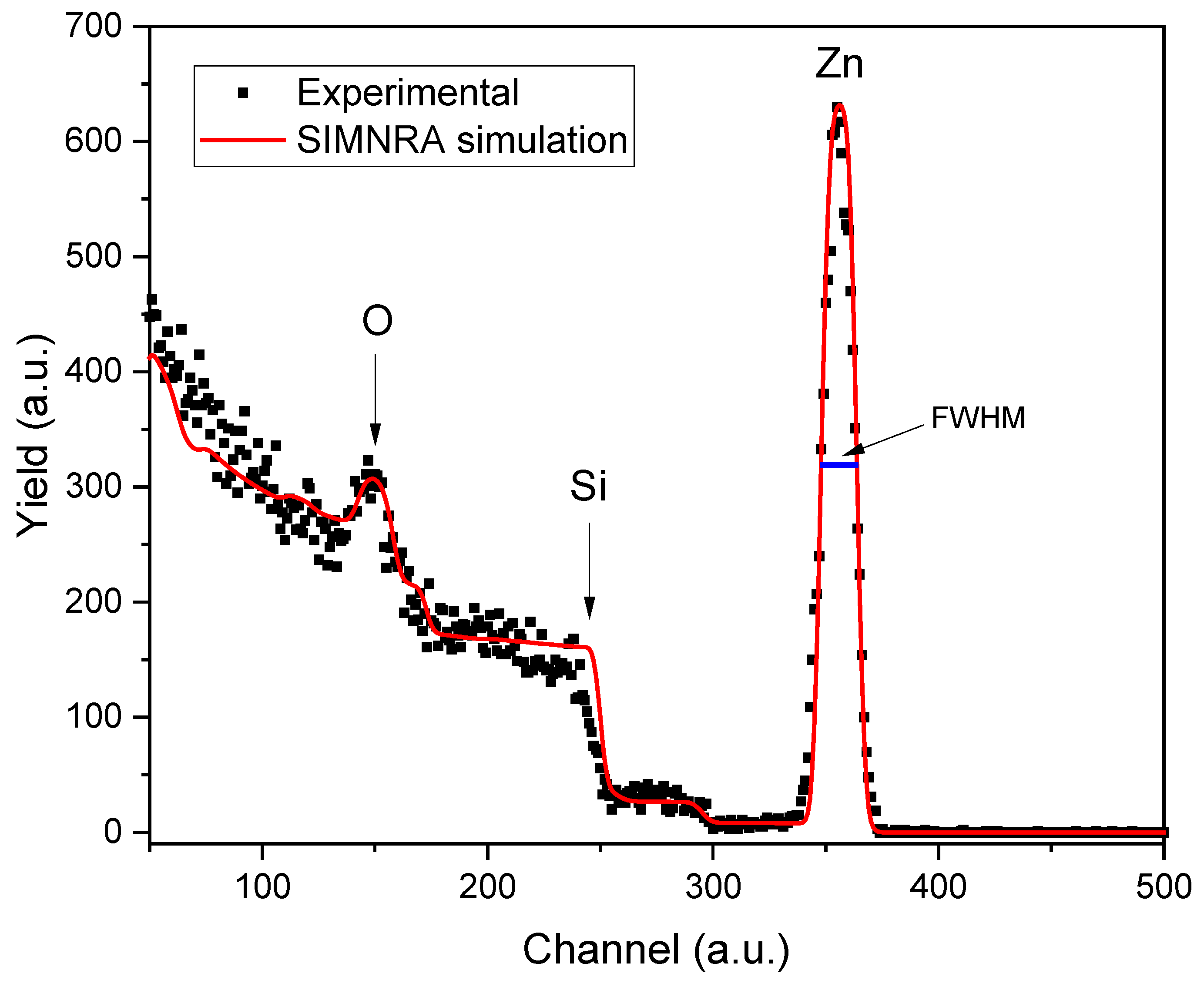
Figure 2.
SRIM simulations. (a) H and Ar atom concentrations in the ZnO thin film, (b) the electronic energy loss (ionization events), and (c) the nuclear energy loss (vacancies and defects).
Figure 2.
SRIM simulations. (a) H and Ar atom concentrations in the ZnO thin film, (b) the electronic energy loss (ionization events), and (c) the nuclear energy loss (vacancies and defects).
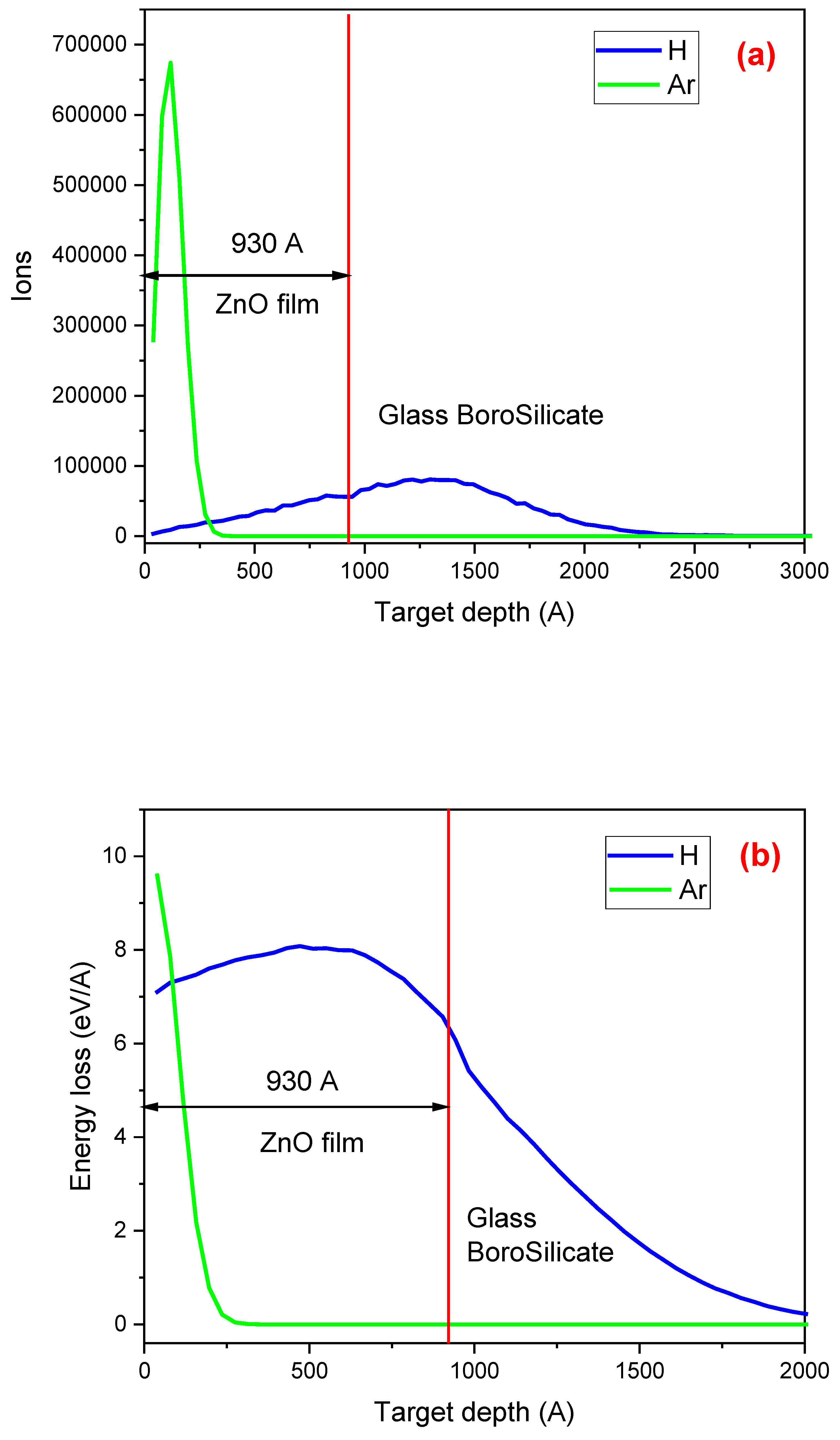
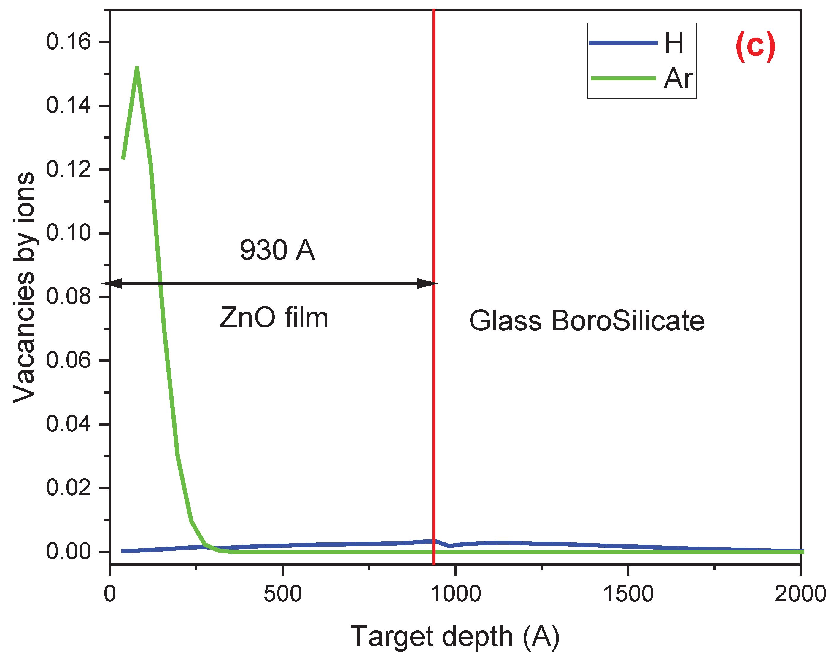
Figure 3.
Optical transmittance spectra of the pristine sample and the films irradiated with H+ and Ar+ ions.
Figure 3.
Optical transmittance spectra of the pristine sample and the films irradiated with H+ and Ar+ ions.
Figure 4.
XRD Diffractograms of the pristine and the irradiated samples.
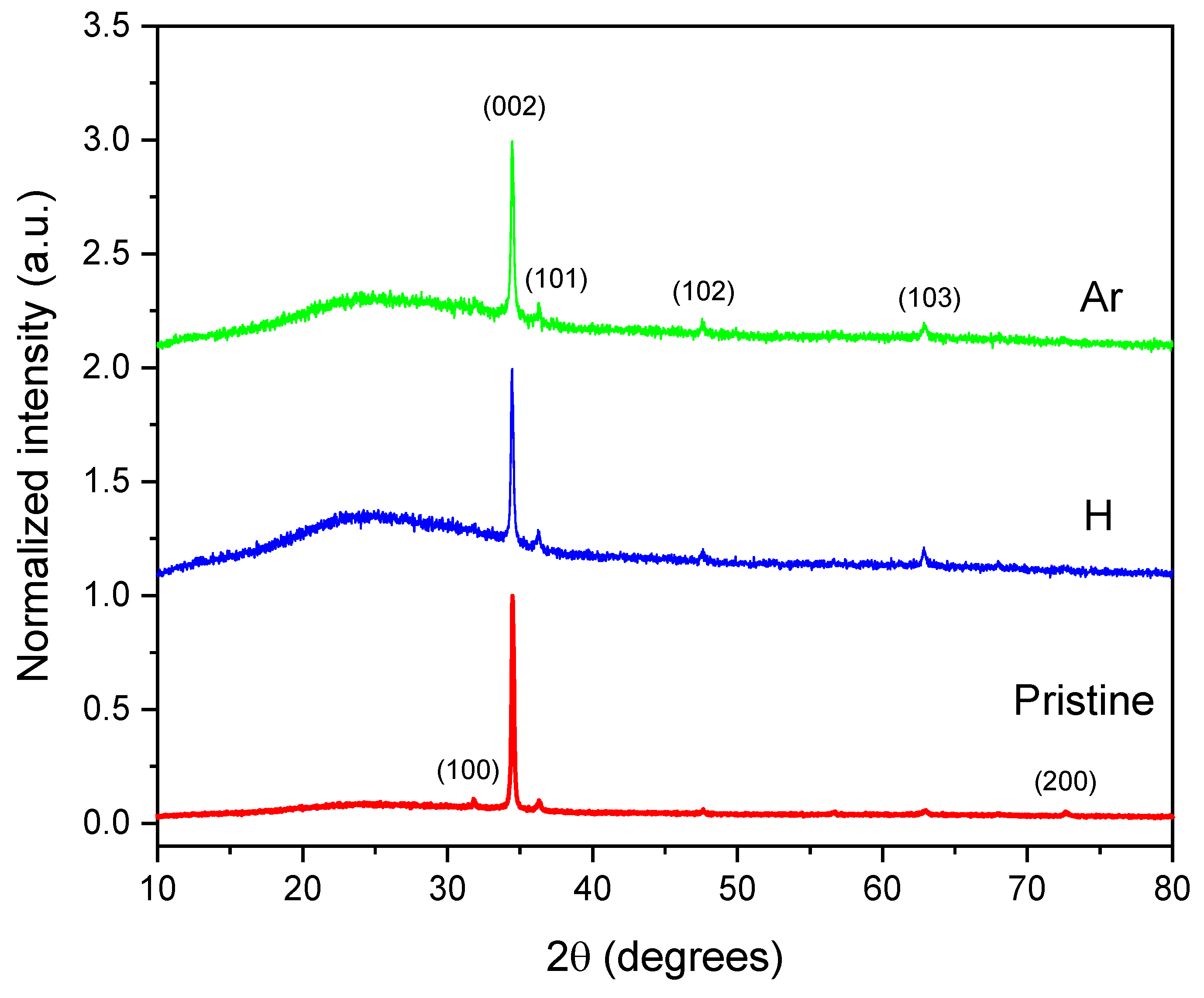
Figure 5.
SEM micrographs of ZnO thin films (a) pristine, (b) irradiated with H+ ions, and (c) irradiated with Ar+ ions.
Figure 5.
SEM micrographs of ZnO thin films (a) pristine, (b) irradiated with H+ ions, and (c) irradiated with Ar+ ions.
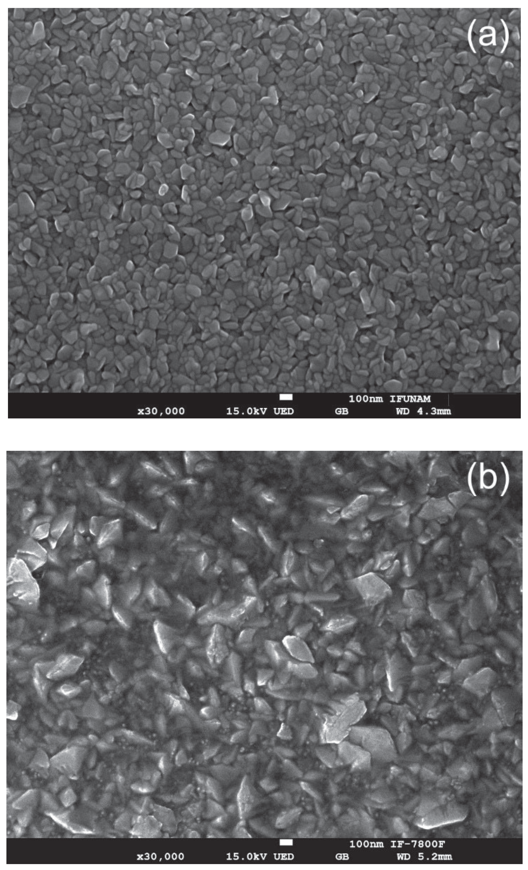
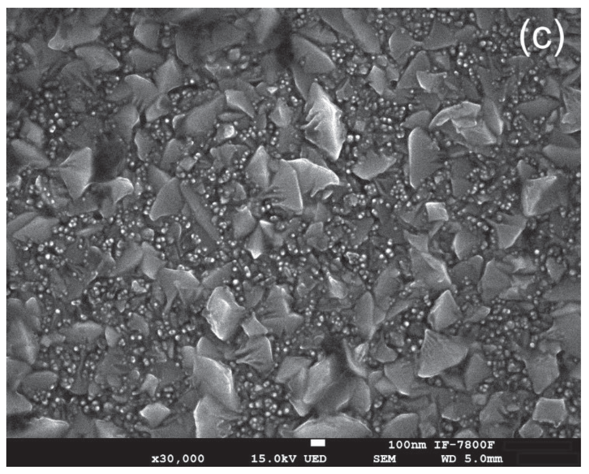

Table 1.
Energy band gap values of the pristine and H+ and Ar+ irradiated samples.
| Irradiated ion | Energy band gap (eV) |
| None (pristine) | 3.300 |
| H+ | 3.281 |
| Ar+ | 3.277 |
Table 2.
Lattice constants and the average crystallite size of the pristine and irradiated ZnO films.
Table 2.
Lattice constants and the average crystallite size of the pristine and irradiated ZnO films.
| Irradiated ion | a (Å) | c(Å) | c/a | Average crystallite size (nm) |
| Pristine | 3.244 | 5.196 | 1.60 | 46.22 |
| H+ | 3.240 | 5.204 | 1.61 | 32.04 |
| Ar+ | 3.240 | 5.204 | 1.61 | 28.68 |
Disclaimer/Publisher’s Note: The statements, opinions and data contained in all publications are solely those of the individual author(s) and contributor(s) and not of MDPI and/or the editor(s). MDPI and/or the editor(s) disclaim responsibility for any injury to people or property resulting from any ideas, methods, instructions or products referred to in the content. |
© 2025 by the authors. Licensee MDPI, Basel, Switzerland. This article is an open access article distributed under the terms and conditions of the Creative Commons Attribution (CC BY) license (http://creativecommons.org/licenses/by/4.0/).
Copyright: This open access article is published under a Creative Commons CC BY 4.0 license, which permit the free download, distribution, and reuse, provided that the author and preprint are cited in any reuse.


