
Submitted:
15 August 2025
Posted:
18 August 2025
You are already at the latest version
Abstract
The structure and composition of a refractory Ni-containing CrMoNbTaVW high entropy alloy (HEA) thin film were investigated. The HEA thin film with a thickness of 5 μm was grown by magnetron sputtering from a multiple-elemental compound target. The Ni-containing HEA thin film with a Ni concentration of 3.6 at. % exhibits a single-phase body-centered cubic (BCC) crystal structure with a lattice parameter of a = 0.316 nm. The grains in the HEA thin film are columns, extended in the growth direction. They are not exact perpendicular to the substrate surface. The thin film grows in a polycrystalline structure with a tendency to preferred orientation or texture. Energy-dispersive X-ray analyses of the HEA thin film show near equal atomic concentrations of Cr, Mo, Nb, Ta, V, W elements in the range 15-17 at. % with almost uniform distribution. In contrast, Ni is not uniformly distributed in the film, and grains with a different Ni-concentration were observed. The defects, observed in the HEA layer are mainly single dislocations or an assembly of dislocations, which could be caused by residual stresses in the layer during the growth of the HEA thin film.
Keywords:
refractory high entropy alloy
; thin films
; magnetron sputtering
; electron microscopy
1. Introduction
High entropy alloys (HEA) consisting predominantly of refractory elements with high melting points such as Hf, Mo, Nb, Ta, V, Zr and W, are generally considered as refractory HEA and are discussed in literature with strong emphasis. Refractory HEA first proposed by Senkov et al. in 2010 [1], have attracted attention due to their versatile properties, such as good mechanical properties, excellent anti-oxidation performance, outstanding corrosion resistance, and high thermal stability, indicating huge application potentials, both in form of bulk and thin film materials [1,2,3,4,5,6,7,8,9,10]. Individual multiple-principle element alloy bulk and thin film materials representing different mixtures of four, five or six refractory metals of the group Cr, Mo, Nb, Ta, V and W were already exemplarily and systematically investigated [1,2,3,4,5,6,7]. For example, MoNbTaW multiple-principle element alloysand MoNbTaVW HEA with equiatomic concentrations of elements prepared by arc-melting have been shown to form a single-phase body-centered cubic (BCC) structure and to maintain its chemical homogeneity with good mechanical properties [1,2,3]. Different 5-elemental refractory HEA thin films based on the MoNbTaW+X system with thicknesses of 300-400 nm and grown by magnetron sputtering were investigated in [4]. The additional element X used was Ti, V, Cr, Mn or Hf. All films showed a BCC structure with a lattice parameter in range of 0.32-0.33 nm and a dense columnar morphology. In [5], it was shown that the refractory HEA thin films based on the multi metal system MoNbTaW are promising materials for high temperature applications where a high thermal stability is important. 6-elemental CrMoNbTaVW HEA thin films with a single-phase BCC structure, created by combinatorial synthesis, was reported in [6] along with a study of the mechanical properties of the thin films in dependence on different concentrations of elements. In [7], it was predicted on basis of thermodynamical calculations and simulations that CrxMoNbTaVW HEA can be tailored over a certain range of Cr content with the BCC structure.
The pronounced high room temperature brittleness of refractory HEAs is however a key factor restricting their application. Previous studies have shown that the addition of Ti and Ni can effectively reduce the room temperature brittleness of refractory HEAs. Zhang et al. [11] investigated the effects of adding Ti and Ni on the microstructure and high-temperature mechanical properties of NbMoTa-based refractory HEAs and showed improvement of the mechanical properties of the alloy upon such chemical modification. This emerging field of such new, specifically alloyed HEA materials is by far not yet systematically explored.
In this work, the microstructural characterization of a magnetron-sputtered 6-elemental CrMoNbTaVW thin film of near-equiatomic concentration and modified with a small amount of Ni was carried out by X-ray diffraction, scanning and transmission electron microscopy. It is demonstrated, that this Ni-alloyed thin film exhibits a solid solution BCC structure.
2. Material and Experimental Techniques
The investigated thin film with thickness of ~ 5 μm was grown by d.c. magnetron sputtering from a multiple-elemental compound target with concentrations of Cr, Mo, Nb, Ta, V, W in the range 11-20 at. % and ~ 10 at. % of Ni. The target diameter was 75 mm, and the target power was 500 W d.c. The thin film deposition was carried out on the cemented carbide substrate in a pure argon atmosphere with an argon gas flow of 30 sccm and a pressure of 0.2 Pa. The substrate temperature was 350 °C. The substrates were grounded during deposition. The residual gas pressure was 0.32 mPa. Before the actual coating process started, the substrates were ultrasonic-cleaned in acetone and plasma-etched with argon ions.
Structural characterization of thin films was carried out by X-ray diffraction (XRD), scanning (SEM) and transmission electron microscopy (TEM). TEM investigations were carried out using Talos F200X microscope equipped with the high-angle annular dark-field (HAADF) detector for scanning TEM (STEM). TEM cross-section samples were prepared using focus ion beam. For the determination of the thin film composition, energy-dispersive X-ray (EDX) spectroscopy was used. For the crystallographic investigations, XRD on a Seifert X-ray diffractometer Space Universal with Cu Kα radiation, conventional TEM with selected area electron diffraction, and high-resolution TEM imaging (HRTEM) with fast Fourier transformation (diffractogram) were applied.
3. Results and Discussion
3.1. Surface Morphology of the Ni-Containing CrMoNbTaVW Thin Film
Figure 1 shows SEM images of the surface of the investigated HEA thin film on different scales.
On the large scale in Figure 1a we observe a very smooth and homogeneous surface of the HEA thin film. This is confirmed by the SEM image on a smaller scale in Figure 1b: it is clearly visible, that the thin film exhibits a surface topography with significant growth features, i.e. a homogeneous, dense columnar structure is indicated. This is supported by further TEM observations (see below Figs. 3 and 4c), which clearly show that the grains in the HEA thin film are columnar with diameters up to few hundred nm. These columnar grains end at the thin film surface and form the topography observed in Figure 1b. The elemental SEM-EDX maps (not shown here) reveal a homogeneous distribution of all elements on both large and small scale. Note, that the SEM-EDX signal is obtained from a large area of the layer with a depth up to 1 μm, which leads to a bulk-like average in the determination of the elemental concentrations. The results of the EDX measurements on the surface in two different areas 1 and 2 of the HEA thin film in Figure 1a and indicated by white rectangles with sizes of ca. 30 μm x 20 μm are presented in Table 1.
We observe almost equal atomic concentrations of the 6 metallic elements Cr, Mo, Nb, Ta, V and W in the HEA thin film in the range 15-17 at. % and a small amount of Ni, ~ 3.6 at. %. It is obvious, that the elemental composition of the thin film deviates significantly from that of the sputter target, especially the Ni concentration of the film is much lower in the HEA thin film than in the target. An explanation of this observation can be found in the plasma conditions applied for the magnetron sputter deposition, which depends clearly on gas pressure, gas flow, substrate temperature, target-to-substrate distance and magnetic field configuration at the target.
3.2. Structure of the Ni-Containing CrMoNbTaVW Thin Film
Figure 2 shows X-ray diffraction (a) and electron diffraction (b) patterns of HEA thin film.
All diffraction peaks on the X-ray diffraction pattern obtained from the Ni-containing HEA thin film in Figure 2a and the diffraction circles and spots from the large area of the thin film cross-section TEM sample in Figure 2b have been identified as belonging to a perfect body centered cubic (BCC) phase. The indexes of the crystal planes corresponding to the XRD peaks are indicated in Figure 2a. Usually, for uniform homogeneous materials, the intensity of the XRD peaks decreases with increasing lattice plane indexes. Texture can be recognized as an enhancement of the relative intensity of some Bragg reflections and a reduction of others. In Figure 2a, we observe a higher intensity of the (110), (211) and (321) peaks, which reveals a tendency to a growth with preferred orientation or even the presence of textures of these crystal planes in the investigated HEA thin film. The identical lattice planes of the BCC crystal structure are displayed and indexed in the electron diffraction pattern in Figure 2b, obtained from large area of the cross-section TEM sample. Here, besides with strong (110) spots, we also observe many spots of (211) and (321) reflections, that also support the statement on its texture. The lattice parameter of the BCC phase, determined from Figure 2a and Figure 2b is a = 0.316 ± 0.001 nm.
Figure 3 shows a cross-section HAADF image of the HEA thin film, that was oriented parallel to the substrate surface (horizontal edge).
The grains of the thin film are columns, extended in growth direction but not exactly perpendicular to the substrate surface. The width of the grains is changed in the growth direction and reaches a few hundred nm. This geometrical appearance of the V-shaped columnar grains matches well the growth of magnetron sputtered thin films. Further, we observe dislocations inside the grains. These are single dislocations inside the grains (please see a grain in Figure 3 on the left side with dislocations indicated by white arrows and marked as D1), while other grains contain assemblies of the dislocations (please see a grain in Figure 3 on the right side with dislocations indicated by white arrows and marked as D2), which are parallel and arranged in the same planes. Similar groups of dislocations in another area of the thin film are shown in Figure 6 (see below). Such phenomenon is often observed when compressive residual stresses have developed during the growth of the thin films.
Figure 4 shows a HRTEM image of the HEA thin film with evaluated (left hand side) and simulated (right hand side) diffractograms from the area marked by the white square in the HRTEM image and the corresponding enlarged point pattern of the HRTEM image. The simulation of the diffractogram shows a BCC crystal structure close to [111]-zone axis orientation.
In Figure 4a we see only a part of a columnar grain, which is elongated in the growth direction and cropped from the top during the FIB preparation of the TEM sample. The comparison of the HRTEM image in Figure 4a with the identically oriented bright-field overview image in Figure 4c shows, that the grain in Figure 4a is elongated in <110> crystal direction of the HEA thin film.
It is known, that in pure BCC metals the {110} crystal planes have a lowest surface energy [12]. Raabe [13] has observed {110}, {211} and {321} rolling textures of BCC metals in his simulations and related them to the activation of slip systems. In the BCC crystal structure, which was clearly identified as the only crystalline phase of the investigated HEA thin film, there are three slip systems that can be activated during plastic deformation: {110}<111>, {211}<111>, and {321}<111>. The activation of these slip systems depends on factors such as the temperature, strain rate, chemical composition, and crystal orientations [14]. The slip in a BCC structure occurs always in the closest packed ⟨111⟩ direction. As an example, in BCC Ta slip is predominantly on the {110} planes at low temperatures. As temperature increases, slip is observed on the {110}, {211} and {321} planes at room temperature and higher temperature. The transition temperature from the {110} to the {112} slip has been found to be between 100 K and room temperature especially for tantalum materials [15,16,17]. The dominant dislocation slips on the {211} planes were experimentally observed in tantalum single crystals under compression at room temperature [16]. The breakdown of so-called Schmid’s law (slip on {110} plans) was reported for group V and VI BCC transition metals, by numerous atomistic simulations and physically informed continuum crystal plasticity model studies [17,18]. The main reason for non-Schmid behaviour in transition metals was revealed to be the cores of 1/2<111> screw dislocations spreading on various {110} planes in the <111> zone.
In many component BCC crystals, consisting of group V and VI BCC refractory metals, the slip is not studied in detail. So, in the case of 4-component NbMoTaW columnar thin films [19,20], it has been generally observed that slip activity predominantly occurs on {110} planes at room temperature. The columns were mainly extended in <110> growth direction.
Our investigated complex HEA thin film contains 6 refractory metals with an additional small Ni amount. It has also a perfect BCC structure. The increased intensities of some XRD peaks in Figure 2a and the presence of solid spots in the electron diffraction pattern in Figure 2b reveal the presence of a texture of {110}, {211} and {321} crystal planes in the investigated HEA thin film. In general, a texture can be due to templating from the crystalline orientation of the substrate, minimizing the surface energy during deposition, or the competition between surfaces with anisotropic growth rates from grains with different orientations. In our case, the substrate has large grains with sizes higher than 1 μm (Figure 4c). The different crystal planes of the substrate grains can come to the substrate - HEA thin film interface We carried out XRD analyses also of the pure substrate (not shown here) and found that one peak from crystal planes of the substrate exactly corresponds to {211} peak of the investigated HEA layer. It means, that there are crystal planes in the substrate and in the HEA thin films with the same lattice plane distance. Close to the XRD {321} peak of the HEA thin film there is also a small peak from the substrate. The other peaks are far apart. Thus, the texture of the {110} crystal planes can be explained by their lowest surface energy, meanwhile the texture of the {211} and {321} crystal planes may be caused by the “epitaxial growth” of the HEA thin film on the substrate.
From the other side, during the growth of the HEA thin film the columnar grains extend also in perpendicular direction and contact each other with different crystal planes, which leads to stress or deformation in the layer. Deformation mechanisms in BCC materials are primarily related with slip deformation. In the investigated HEA thin film we observe assemblies of dislocations in Figs. 3 and 6, which are arranged on {110} slip planes. This reveals plastic deformation inside the layer during the growth of the different textured grains. Thus, the activation of the all slip systems may play a role in the formation of {110}, {211} and {321} textures in the investigated HEA thin films.
3.2. Composition of the Ni-Containing CrMoNbTaVW Thin Film
An HAADF STEM image of the HEA thin film and elemental EDX maps are presented in Figure 5. EDX measurements of the HEA thin film in TEM on the small scale show almost equal atomic concentrations of Cr, Mo, Nb, Ta, V and W elements of around 15-17 at. % with uniform distribution as well as we have observed in SEM on the large scale (s. Table 1). On the Ni-map, there are regions with changing Ni-concentration, which are indicated by arrows in Figure 5. The local measurements of Ni-concentration in the thin film are in range 0.5 at. % to 4.7 at. %. Considering the thickness averaging in TEM samples along the electron beam, regions without Ni could exist.
Note, that the constituting metals Cr, Mo, Nb, Ta, V and W originally have BCC crystal structures, while Ni has face-centered cubic crystal structure. From a thermodynamic equilibrium point of view, Ni has different solubilities with the individual metals and it may not match with the BCC crystal structure of the investigated HEA thin film. Moreover, the solubility of Ni may be low for such complex systems as the 6-elemental HEA. Considering the kinetics of thin film formation in physical vapor deposition, especially in magnetron sputtering processes (i.e. reflecting very high colling rates up to 1013 K/s from the vapor phase), the solubility of Ni in such alloys could be enhanced. The key question is up to what concentration Ni can be dissolved in the BCC structure and whether it is energetically more favorable for Ni to be dissolved in the BCC crystal or to accumulate at the grain boundaries. These three factors may contribute to the inhomogeneity of the Ni-distribution, which we observe in elemental EDX maps in Figure 5.
For the determination of an exact location of Ni, inside grains or at grain boundaries, an EDX analysis on larger scale was carried out. This is presented in Figure 6.
Like in Figure 3, in the inverted HAADF STEM image in Figure 6 there are groups of dislocations, which are reflected by dark lines and marked by white arrows and annotated as D. In the EDX maps, beside almost the homogeneous distribution of the elements Cr, Mo, Nb, Ta, V and W, we observe a changing Ni-concentration in the range 3.35 at, % to 4.65 at. % perpendicular to the columnar grains. Two peaks of maximums of the Ni-concentration from right hand side are observed in ~ 50 nm wide regions, whereas regions with increasing Ni-concentration from left hand and decreasing Ni-concentration in middle of the linescan are more than 200 nm wide. The existence of Ni-rich areas with a small variation of only ca. 1 % with sizes comparable with the grain width observed in Figure 6 does not allow to finally conclude about a possible Ni-segregation at the grain boundaries in the investigated HEA thin film. Note, that the distributions of Cr, Mo, Nb, Ta, V and W along the linescan (here are not shown) is also varied in the range up to 2%. Moreover, it was shown in [11], that the solubility of Ni in similar, but only in 3 component NbMoTa refractory HEA, occurs up to 45 at. % over wide range of temperatures. Therefore, and with regard of the present XRD and TEM analyses shown, we suggest that in our investigated HEA thin film grains with a different Ni-concentration exist. The structural model for the HEA thin film of this investigation is a single-phase solid solution in BCC structure with 3.6 at. % Ni incorporated in the BCC crystal.
4. Conclusions
In this study, a novel, complex refractory Ni-containing CrMoNbTaVW HEA thin film was investigated. The single-phase HEA thin film has a perfect BCC crystal structure. The HEA thin film has columnar grains with texture of {110}, {211} and {321} crystal planes. Variation of the Ni-concentration in the HEA thin film with higher solubility in the crystal and lower concentration at the grain boundaries. was observed. The defects, observed in the HEA thin film are mainly single or an assembly of dislocations, that are mainly caused by stresses of the thin films resulting from its growth.
Acknowledgments
This work has been carried out within the framework Helmholtz-Programm MTET.
References
- N. Senkov, G. B. Wilks, D. B. Miracke, C. P. Chuang, P. K. Liaw. Refractory high-entropy alloys. Intermetallics 18(9) (2010) 1758-1765. [CrossRef]
- O. N. Senkov, G. B. Wilks, J. M. Scott, D. B. Miracle, Intermetallics 19 (2011) 698-706, Mechanical properties of Nb25Mo25Ta25W25 and V20Nb20Mo20Ta20W20 refractory high entropy alloys. [CrossRef]
- A. Poulia, E. Georgatis, A. Lekatou, A. E. Karantzalis, Int. Journal of Refractory Metals and Hard Materials 57 (2016) 50–63, Microstructure and wear behavior of a refractory high entropy alloy. [CrossRef]
- Georg C. Gruber, Alice Lassnig, Stanislav Zak, Christoph Gammer, Megan J. Cordill, Robert Franz, Synthesis and structure of refractory high entropy alloy thin films based on the MoNbTaW system, Surface and Coatings Technology, Volume 439, 2022, 128446. [CrossRef]
- Georg C. Gruber, Alice Lassnig, Stanislav Zak, Christoph Gammer, Megan J. Cordill, Robert Franz, Thermal stability of MoNbTaTiW, MoNbTaVW and CrMoNbTaW thin films deposited by high power impulse magnetron sputtering, Surface and Coatings Technology, Volume 454, 2023, 129189. [CrossRef]
- S. Schweidler, P. Reiser, E. Boltynjuk, S. A. Singaraju, F. Fischer, H. Hahn, P. Friederich, L. Velasco, Synthesis and Characterization of High-Entropy CrMoNbTaVW Thin Films Using High-Throughput Methods, Adv. Eng. Mater. 2023, 25, 2200870. [CrossRef]
- B. Zhang, M. C. Gao, Y. Zhang, S. M. Guo, CALPHAD: Computer Coupling of Phase Diagrams and Thermochemistry 51 (2015) 193–201, Senary refractory high-entropy alloy CrxMoNbTaVW. [CrossRef]
- D. B. Miracle, O. N. Senkov, A critical review of high entropy alloys and related concepts Acta Materialia 122 (2017) 448-511. [CrossRef]
- Xiaochang Xie, Neng Li, Wei Liu, Shuai Huang, Xiaoyong He, Qiuying Yu, Huaping Xiong, Enhui Wang, Xinmei Hou, Research Progress of Refractory High Entropy Alloys: A Review, Chinese Journal of Mechanical Engineering (2022) 35:142. [CrossRef]
- B. Chen, L. Zhuo, Latest progress on refractory high entropy alloys: composition, fabrication, post processing, performance, simulation and prospect, Int. J. Refract. Met. Hard Mater., 110 (2023), 105993. [CrossRef]
- H. Zhang, Y.Z. Zhao, J.L. Cai, S.K. Ji, J.L. Geng, X.Y. Sun, D.C. Li, High-strength NbMoTaX refractory high-entropy alloy with low stacking fault energy eutectic phase via laser additive manufacturing, Mater. Des. 201 (2021), 109462. [CrossRef]
- Su-Hyun Yoo, Ji-Hwan Lee, Young-Kwang Jung, Aloysius Soon, Exploring stereographic surface energy maps of cubic metals via an effective pair-potential approach Phys. Rev. B 93, 2016_035434. https://10.1103/PhysRevB.93.035434.
- D. Raabe, Simulation of rolling textures of b.c.c, metals considering grain interactions and crystallographic slip on {110}, {112} and {123} planes, Materials Science and Engineering A 197 (1995) 31-37. [CrossRef]
- D. Hull, D. J. Bacon. Dislocations in other crystal structures. Introduction to dislocations, 2001, S. 102-127.
- Seunghyeon Lee, Hansohl Cho, Curt A. Bronkhorst, Reeju Pokharel, Donald W. Brown, Bjørn Clausen, Sven C. Vogel, Veronica Anghel, George T. Gray, Jason R. Mayeur, Deformation, dislocation evolution and the non-Schmid effect in body-centered-cubic single- and polycrystal tantalum, International Journal of Plasticity,163, 2023, 103529. [CrossRef]
- Hojun Lim, Jay D. Carroll, Joseph R. Michael, Corbett C. Battaile, Shuh Rong Chen, J. Matthew D. Lane, Investigating active slip planes in tantalum under compressive load: Crystal plasticity and slip trace analyses of single crystals, Acta Materialia, 185, 2020, 1-12. [CrossRef]
- C. R. Weinberger, B. L. Boyce, C. C. Battaile. Slip planes in bcc transition metals. International Materials Reviews. 2013;58(5):296-314. https://doi:10.1179/1743280412Y.0000000015.
- Shiyuan Zhou, Shifeng Liu, Yuping Ding, Yahui Liu, Chao Deng, Zhiqing Zhang, Xiaoli Yuan, Microstructure and twinning behavior of b.c.c tantalum under dynamic plastic deformation, Materials Science and Engineering: A, 876, 2023, 145156. [CrossRef]
- Yuan Xiao, Yu Zoub, HuanMa, Alla S. Sologubenko, Xavier Maeder, Ralph Spolenak, Jeffrey M. Wheeler, Nanostructured NbMoTaW high entropy alloy thin films: High strength and enhanced fracture toughness, Scripta Materialia 168 (2019) 51–55. [CrossRef]
- Y. Zou, H. Ma, R. Spolenak, Ultrastrong ductile and stable high-entropy alloys at small scales, Nat. Commun. 6 (2015) 7748. [CrossRef]
Figure 1.
SEM images of the surface of HEA thin film on large (a) and small (b) scales. By white rectangles in (a) indicated areas 1 and 2 of EDX measurements, presented in Table 1.
Figure 1.
SEM images of the surface of HEA thin film on large (a) and small (b) scales. By white rectangles in (a) indicated areas 1 and 2 of EDX measurements, presented in Table 1.
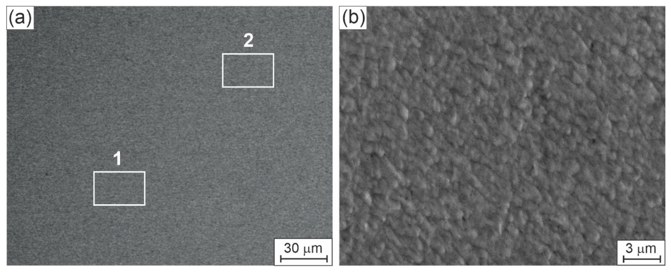
Figure 2.
(a) X-ray and (b) electron diffraction patterns of the Ni-containing HEA thin film. The indexed peaks belong to a BCC crystal lattice with lattice parameter a = 0.316 nm.
Figure 2.
(a) X-ray and (b) electron diffraction patterns of the Ni-containing HEA thin film. The indexed peaks belong to a BCC crystal lattice with lattice parameter a = 0.316 nm.
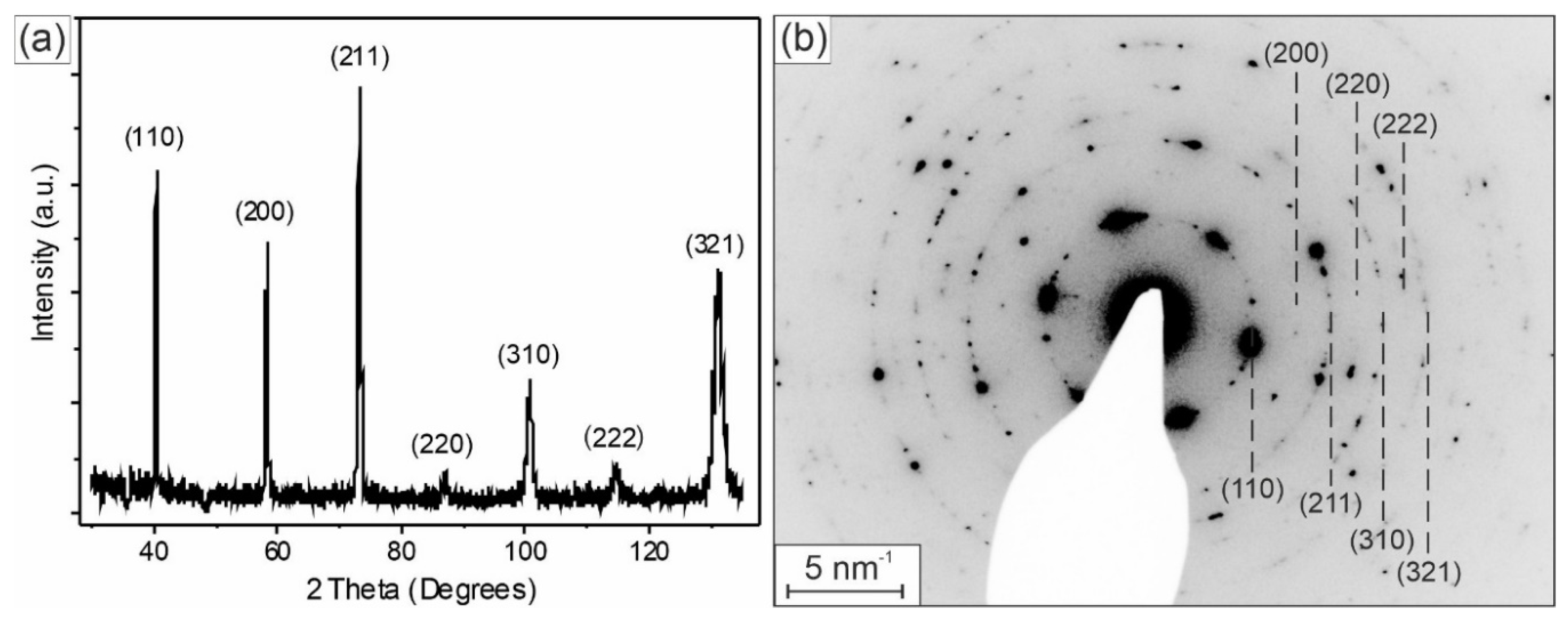
Figure 3.
HAADF STEM image of the HEA thin film. Dislocations are marked by D1 and D2.
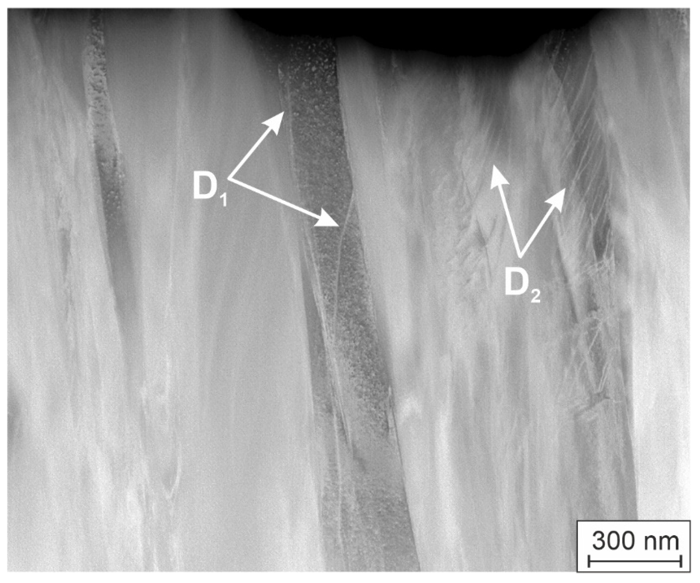
Figure 4.
(a) HRTEM image of the HEA thin film close to the [111]-zone axis orientation of the BCC structure with measured (right) and simulated diffractograms of the area marked by a white square, (b) filtered enlarged HRTEM image, (c) bright-field overview image with substrate (left) and HEA thin film (right). The dashed lines show the <110> crystal direction of the HEA thin film.
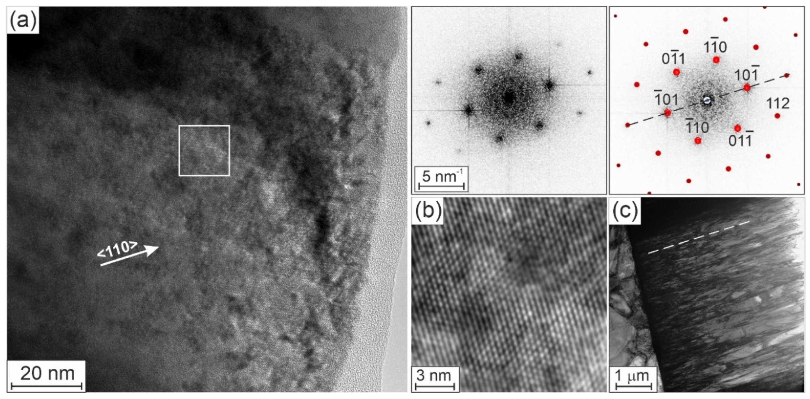
Figure 5.
HAADF STEM image of the HEA thin film with elemental EDX maps. Arrows mark Ni-poor areas.
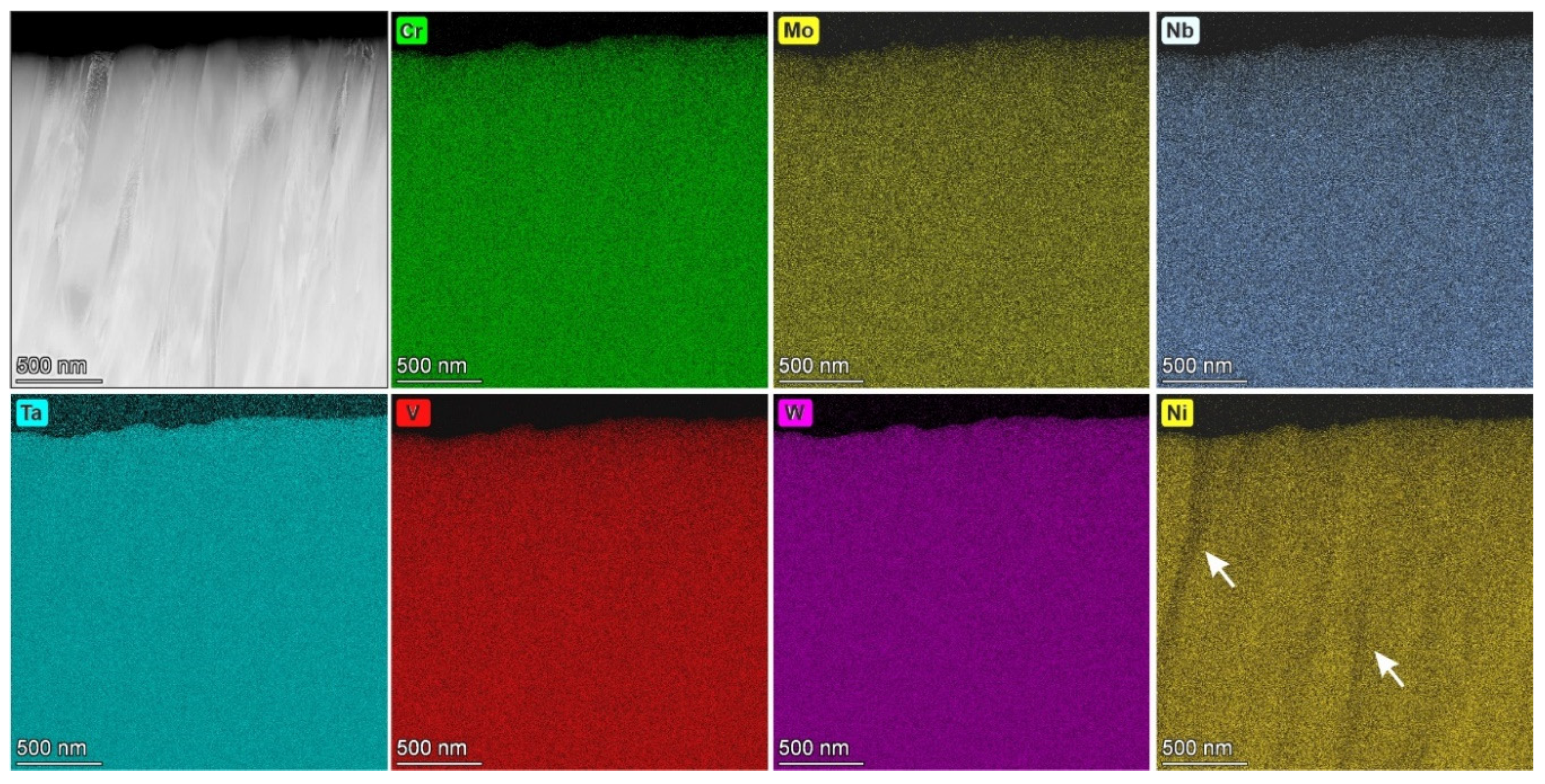
Figure 6.
Inverted HAADF STEM image of the HEA thin film with elemental EDX maps. The arrows mark a linescan of the measured Ni-concentration. The boundaries of Ni-rich areas are indicated by white dashed lines. The maximums and minimum of the Ni-concentration in the linescan are marked by black dashed lines. White arrows annotated as D mark dislocations.
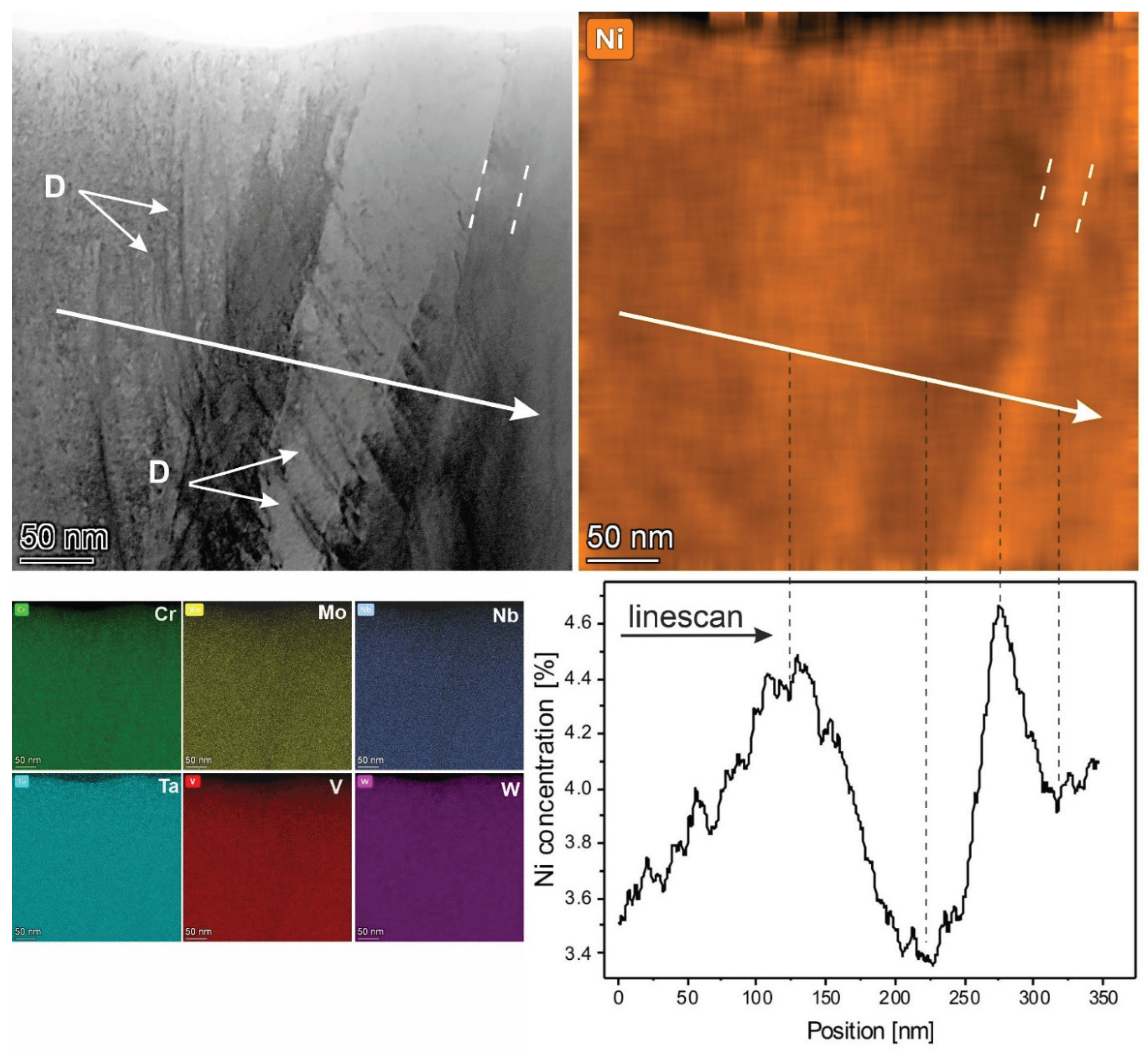

Table 1.
SEM-EDX analyses of atomic concentrations of all elements in areas 1 and 2 of the HEA thin film from Figure 1a.
Table 1.
SEM-EDX analyses of atomic concentrations of all elements in areas 1 and 2 of the HEA thin film from Figure 1a.
| Element | Cr | Mo | Nb | Ta | V | W | Ni |
|---|---|---|---|---|---|---|---|
| at (%), 1 | 15.90 | 15.20 | 15.36 | 17.06 | 16.57 | 16.36 | 3.56 |
| at (%), 2 | 15.74 | 15.11 | 15.42 | 17.34 | 15.44 | 17.30 | 3.65 |
Disclaimer/Publisher’s Note: The statements, opinions and data contained in all publications are solely those of the individual author(s) and contributor(s) and not of MDPI and/or the editor(s). MDPI and/or the editor(s) disclaim responsibility for any injury to people or property resulting from any ideas, methods, instructions or products referred to in the content. |
© 2025 by the authors. Licensee MDPI, Basel, Switzerland. This article is an open access article distributed under the terms and conditions of the Creative Commons Attribution (CC BY) license (http://creativecommons.org/licenses/by/4.0/).
Copyright: This open access article is published under a Creative Commons CC BY 4.0 license, which permit the free download, distribution, and reuse, provided that the author and preprint are cited in any reuse.


