
Submitted:
15 August 2025
Posted:
19 August 2025
You are already at the latest version
Abstract
Several industrial applications rely on induction motors to carry out processes essential for product manufacturing. Speed control of an induction motor commonly requires a pulse width modulated inverter capable of driving a system with long cables, suppression of common mode voltage, reduction of common mode current, and suppression of electromagnetic interference. This paper proposes a three-phase motor drive aimed to make constant the common mode voltage. The proposed system consists of two three-phase conventional full bridge inverters connected in parallel and having as an input two separate direct current sources. The proposed system is controlled by using the space vector pulse width modulation technique. By designing the adequate signal sequences of the switches for both converters, it is possible to keep constant the common model voltage and therefore reduce the associated common mode current making the system more reliable. The proposed system is validated through numerical simulations and by the implementation of an experimental prototype. Low common mode current values as low as 83mA are obtained in both simulations and experiments.
Keywords:
common mode voltage
; induction machine
; leakage ground current
; space vector PWM
; three-phase PWM inverter
1. Introduction
Power electronic drives are widely used for controlling AC induction machines, particularly in industrial processes where variable speed control and high energy efficiency are essential. In recent years, the electric vehicle industry has grown significantly, reaching sales of around 14 million in 2023, contributing to sustainability by helping to mitigate global warming [1,2]. Power electronic motor drives are used to move and control the speed of electric vehicles, improving both speed regulation and motor efficiency by adjusting the frequency and magnitude of the output voltage [3,4]. Typically, conventional three-phase inverters are used as motor drives, due to their inherent simplicity and power flow in either direction. However, this topology has been less used due to its common mode voltage (CMV) and common mode current (CMC) issues [5,6].
In a star-connected three-phase electric induction machine, the CMV is defined as the voltage of the neutral point of the load concerning a common node in the circuit which can be the midpoint of the inverter DC bus. This, in turn, produces CMC that flows to the ground through parasitic capacitances between the stator windings and the motor case [7,8,9]. This phenomenon may cause several issues, such as damage to motor bearings, increased electromagnetic interference, and unwanted ground-fault shutdowns. For these reasons, low transitions and magnitude of CMV and thereby CMC are key to guarantee a good performance of motor drive systems [10,11,12]. To adress these issues, there are different proposals in the literature including passive solutions, topology structure, sinusoidal pulse width modulation (PWM) strategies, Space Vector PWM techniques (SVPWM), active circuits and control methods [13,14,15,16]. Concerning topology-based solutions dealing with the CMV issue, in [17] a double-bridge three-phase inverter fed by a single DC source is proposed. In this configuration a SVPWM technique is used to control both bridges simultaneously, where the null vectors are constructed by using a combination of opposite active vectors. Then, a full match must be ensured between the vectors generated by both inverters to guarantee a proper operation. Therefore, the design of the control system and control algorithms is complex limiting the applications of the presented system. In [18] the H10 inverter is presented which consists in a full-bridge two-level three-phase inverter plus an active circuit at the DC input formed by two half-bridge circuits. The DC source requires three different DC sources connected in series where the active circuit clamps the full-bridge structure achieving constant CMV. However, the DC source must be designed to meet specific voltage levels, which make its implementation challenging. Moreover, in reference [19] two SVPWM strategies are proposed for a modified H10 topology. The main difference regarding [18] is that the DC bus power supply can be now implemented using two symmetric DC sources which expands the possible applications of this topology. The new H10 topology requires specific SVPWM strategies which are designed to provide a reduced magnitude of the CMV. In addition, the two proposed SVPWM deals with the CMV jumps issue due to the dead-time by clamping the CMV when entering and leaving the null vectors.
An asymmetric three-phase inverter topology is presented in [20] consisting of a full-bridge inverter with one leg modified. The modified leg is divided into two parts, the first, introduce a switched capacitor unit which consists of two switches, two diodes and two capacitors and the second includes two switches operating at the line frequency. The switched capacitor unit enables the boosting capability and a three-voltage level leg which contributes to improve the phase current total harmonic distortion (THD), however, the analysis of the CMV is not included for this topology. Finally, [21] proposes a four-leg, two-level three-phase inverter. The proposed structure significantly reduces the CMV component, however due to the required additional leg, an additional LC or LCL filter is also required, namely, increasing the cost, size and weight of the total system.
This paper proposes a motor drive system that consists of two main modules connected in parallel, each module has a two-level three-phase full-bridge inverter having as an input two separated DC sources. Each module includes a DC decoupling circuit that allows the disconnection of the DC source during the application of null vectors. By designing a specific sequence of the space vectors the total CMV of the system can be kept constant and the CMC achieves magnitudes close to zero. The rest of this paper is organized as follows; Section 2 presents the analysis and model of an induction machine in high frequency to clearly identify its parasitic elements. Section 3 explains and describes the proposed two-level three-phase topology, its advantages and drawbacks, and the different operation modes. In Section 4, the proposed specific space vector based modulation strategy is explained and the corresponding switching signals are derived. Section 5 and Section 6 provide the numerical simulation and experimental results respectively. Finally, Section 7 presents the concluding remarks of this research work.
2. High-Frequency Induction Machine Modeling
In a three-phase inverter, the sum of the three-phase voltages is always different from zero at the neutral point. Consequently, a voltage with the same switching frequency as that of the switches and with a magnitude equal to the input bus voltage appears between the motor’s neutral point and ground [23]. This voltage is called CMV and it is given by,
where , , are the per-phase stator voltages of motor. The CMV variations generate CMC that flow to the ground through the parasitic capacitances. Such capacitances are always present between the stator windings and the stator iron [22,23]. The IEEE Standard 112 was established to obtain test methods and parameters for a low-frequency per-phase T-equivalent induction motor model in Figure 1 [24].
The electrical behavior of the per-phase equivalent circuit of the induction motor shown in Figure 1 is given by the following equations (where is neglected):
where is the phasor of the per-phase stator voltage, and are the per-phase stator and rotor resistances, respectively, and are the per-phase stator and rotor leakage reactance, respectively (with being the electrical pulsation, and the stator and rotor inductances, and M the mutual inductance between the stator and the rotor windings), is the per-phase mutual reactance, is the mechanical slip of the induction motor (with p being the pole pairs and the mechanical speed), and the super index′ stands for the rotor magnitudes reduced to the stator winding.
High-frequency motor models can be mainly divided into two classes, i.e., distributed and lumped parameter models. Based on the analysis of the electrical characteristics inside the motor, the equivalent lumped parameter model can be used to express the distributed parameters model. According to [25], the rotor circuit of electric machines does not contribute at high frequencies, as no flux penetrates the rotor’s magnetic circuit. Hence, a high-frequency model of the motor is shown in Figure 2, where denotes the capacitance between the stator windings and the motor frame and is the stator inter-turn capacitance per phase [22]. Two methods are commonly used to determine the high-frequency parameters of the induction motor [26]; the first is the finite-element method, which requires knowledge of the physical and geometrical characteristics of the conductor and insulation [27], and the second is the experimental method [28].
In addition to the model shown in Figure 2, it is important to consider the motor-bearing model, which is where the CMV is present. Here, the capacitances that represent the model of the motor bearings are: which is the stator to frame capacitance, which is the stator to rotor capacitance, represents the rotor to frame capacitance, models the lubricating grease films existing between each bearing ball and sw represents the non-linear behavior of dielectric-breakdown voltage [22,29]. Figure 3 shows the motor-bearing model, then based on latter model the CMV in that follows is modeled using an equivalent parasitic capacitance connected between the neutral point of the load and the negative terminal of the DC source [30].
3. Proposed Induction Motor Drive
The proposed inverter consists of two conventional full-bridge two-level three-phase inverters connected in parallel sharing the AC side of the system as shown in Figure 4. On the DC side, two separated and isolated power sources are proposed with two switches to perform a decoupling action, this concept can be extended to multiple DC sources at the input of each three-phase inverter allowing, for instance, the balancing capability of a bank of batteries or several arrays of photovoltaic modules. Note that and model the parasitic capacitors of the DC buses, represents the equivalent capacitor of the bearing model and is the ground path impedance. The switches and (A and B) in each DC source are used to perform a decoupling action of the DC input power sources from the AC side of the inverter. On the right side of the DC decoupling circuit, the circuits denoted as and are used to set the appropriate space vector to feed the three-phase induction motor. According to the proposed power circuit, the operation modes of the proposed system can be described as follows. First, the null state can be adopted by configuring the simplified circuit depicted in Figure 5 and taking into account the next three considerations:
- The reference vector is located at the first sector as it is shown in Figure 6,
- The load is predominantly inductive as is the case of an induction motor,
- The space vector sequence is the one that is used for the conventional two-level three-phase inverter.
Note that in this case all the output voltages are equal to zero which corresponds with the freewheeling operation. It can also be observed that is set with an odd active vector which in this case is . At the same time is configured with the next even vector to be applied in the sequence which is with the switches and in the off state. Therefore, the load current is distributed equally between the switches of the two inverters, allowing a well balanced distribution of the power losses.
The second system state is devoted to the application of an active vector, according to the conventional space vector modulation (SVM), the next vector to be applied is , then and are turned on, allowing the output current to flow towards the load as is depicted in Figure 7. As it can be observed the load current flows through the switches , and as in a conventional three-phase full-bridge inverter, while the remains in the same configuration as in the previous state. Moreover, the third state of the proposed drive system, is devoted to the application of the second active vector which is , as is depicted in Figure 8. Then, and are turned off while and are turned on with vector already configured in the previous state, allowing the load current to flow through the switches , and . Finally and according with the conventional SVM sequence, a null vector is applied using the configuration depicted in Figure 9, where the load current can be equally distributed among the semiconductors in both inverters.
The operating states described above are applied each switching period along sector one. This means that, by using only the decoupling switches, the reference vector can be synthesized; therefore, no commutations are required in the remaining switches. Table 1 summarizes the different operation states described above for the proposed system. Moreover, the same vector sequence strategy can be extended to the complete grid period by using the corresponding active vectors to configure each inverter, as it will be explained in the next section.
Summarizing, supplies the odd active vectors along the grid period which according to [31] produce a CMV equal to concerning the node . Moreover, supplies the even active vectors along the grid period which produce a CMV equal to concerning the node . Therefore the magnitude of the CMV is kept constant in each inverter module along the total grid period. Constant CMV does not generate CMC; thus the magnitude of in the proposed system of Figure 4 is close to zero making the proposed system a strong solution for induction motor drive applications.
4. Proposed Modulation Strategy
The modulation strategy is designed based on SVPWM theory. The inverter states described in the previous section are considered to define the modulation sequences shown in Figure 10. As shown, the vector sequences follow the conventional space vector modulation technique. For example, in Sector I, the conventional sequence is V0-V1-V2-V7-V7-V2-V1-V0. However, the proposed SVPWM sequence incorporates the states required by the decoupling switches in each three-phase bridge. Therefore, the vector names have been modified to form a sequence such as SV10-SV11-SV10-SV20-SV21-SV21-SV20-SV10-SV11-SV10. In this case, the odd active vectors, for instance SV11, are supplied by Inverter A, while the even vectors, such as SV21, are supplied to the load by Inverter B. The freewheeling state is achieved by disconnecting both DC sources while maintaining the inverters configured with their respective active vectors. In this way, it is possible to reduce the switching losses improving the inverter efficiency.
For a balanced thee-phase system in Figure 6 can be expressed as follows:
The reference vector can be approximated by using a sequence of three vectors in a switching period (). Such vectors can be the adjacent active vectors and depicted in Figure 6 for Sector I. and are the vectors SV11 and SV21 defined for the specific modulation sequence of the proposed inverter which are depicted in Figure 10. Note that the third vector can be selected from the null vectors and , as shown in Figure 6. These correspond to SV10 and SV20 in Figure 10. The sum of the applied vectors over a switching period is equal to the reference vector , thus,
where and are the active vectors and can be any of the null vectors and the addition of the application times (, and ) must be equal to ,
The duty cycles for each active and null vector can be calculated by analyzing the real and imaginary components of . However, since this theory is extensively covered in the literature [32], it is omitted in this paper.
5. Numerical Results
Simulations using a predominantly inductive load are performed using PSIM software. The numerical results are obtained in an open loop configuration under the parameters listed in Table 2. The developed simulations allow validation of the common mode behavior of the proposed topology. Figure 11 shows the switching pattern along more than two grid periods for the odd switches and the decoupling switches of both inverter modules. The sectors along each period are also included for reference. Note that, if sector 1 is observed, the switching pattern corresponds to that shown in Figure 10, after that, Sector 2 changes to the new active vectors and , and so forth, until the total period is completed. In Figure 12 from top to bottom the output three-phase currents and the common mode current are depicted. Note that, the output currents correspond with a sinusoidal waveform plus the switching ripple expected due to the commutations of the semiconductors. The measured is around which is mainly due to the switching ripple. Moreover, the common mode current presents a small value which is which fulfills the main objective of the proposed system. The line-to-line voltages are depicted in Figure 13 where it can be observed that the waveforms correspond to those typical in a two-level three-phase full-bridge inverter. Additionally, Figure 14 shows, from top to bottom, the parasitic capacitor voltages and and the CMC, . As observed, the voltages across the parasitic capacitors remain constant at values of for and for . These constant voltages are produced by the space vector algorithm used to control the proposed inverter. A dynamic measurement has also been performed, as shown in Figure 15, where a step load change from to is applied. Notably, this power step does not cause transients in the common-mode current, indicating that the proposed system is robust against variations of inverter power.
6. Experimental Results
The experimental validation has been performed by implementing a laboratory prototype. The experimental prototype parameters are the same as those declared in Table 2. The semiconductors of the system are implemented using diode modules STTH200R04TV from STMicroelectronics and IGBT modules SKM50GB12T4 from Semikron. The modulation algorithm is programmed in a Digital Signal Processor (DSP) model TMS320F28335 mounted in a development board designed in the lab and using PSIM. The SVPWM signals are measured at the output of the DSP to validate the algorithm which are shown in Figure 16. As it can be noted, these signals contain the same sequence as in the simulation results, note also that only one grid period is considered. Moreover, Figure 17 shows the experimental three-phase output currents whose waveforms are almost sinusoidal plus the switching ripple as in the simulation results. The CMC is also measured, with an value of , higher than in simulation, due to the presence of passive parasitic components in the circuit. Moreover, experimental results are also obtained for line-to-line voltages. The results are depicted in Figure 18 where the common mode current is also included. The voltage waveforms show the corresponding three-level and the maximum voltage corresponds with as is defined in Table 2.
Voltages across the parasitic capacitors and are depicted in Figure 19. Note that, these voltages are constant as expected according to the proposed SVPWM algorithm. The voltage magnitudes are around and for and respectively, consistent with the simulation results. Finally, to validate the robustness under power changes the experimental results in Figure 20 are also obtained. A step-up power load varying the load resistance from to is applied to demonstrate that the magnitude remains with the same waveform and value.
7. Conclusions
In this paper, a three-phase inverter topology and its space vector modulation strategy were proposed to deal with the common mode current problem in induction motor drives. The proposed system made use of two three-phase two-level full-bridge inverter modules with a DC decoupling circuit. Each module was intended to set the odd active vectors or the even active vectors achieving in this way constant common mode voltage and as a result very low common mode current. An key advantage of the proposed method was that the active vectors can be configured once along a complete sector, then the DC decoupling circuit allows allows the application of both active and zero vectors, thereby reducing power losses. Experimental and simulation results demonstrate that the common mode current was effectively reduced and the independence of the proposed method regarding system power. These results support the conclusion that the proposed inverter topology is well-suited for motor drive systems and transformerless photovoltaic applications.
Author Contributions
All authors contributed to the development of the overall document, space vector modulation design, analysis, simulations, and experimental results. All authors have read and agreed to this version of the manuscript.
Funding
This research was partially funded by Tecnologico Nacional de Mexico under the project 10138.21-PD.
Conflicts of Interest
The authors declare no conflict of interest.
Abbreviations
The following abbreviations are used in this manuscript:
| AC | Altern Current |
| DC | Direct Current |
| PWM | Pulse Width Modulation |
| CMV | Common Mode Voltage |
| CMC | Common Mode Current |
| SVPWM | Space Vector Pulse Width Modulation |
| THD | Total Harmonic Distortion |
| IGBT | Isolated Gate Bipolar Transistor |
| DSP | Digital Signal Processor |
References
- International Energy Agency, “Global EV Outlook 2024, Moving towards increased affordability,” in IEA publications, France, April 2024.
- Y. Yu, Y. Pei, F. Chai and M. Doppelbauer, “Performance Comparison Between Permanent Magnet Synchronous Motor and Vernier Motor for In-Wheel Direct Drive,” in IEEE Transactions on Industrial Electronics, vol. 70, no. 8, pp. 7761-7772, Aug. 2023. [CrossRef]
- S. Mishra, B. Singh and A. Varshney, “Adaptive Flux Based Speed Estimation of Syn-Rel Motor Drive for Electric Vehicle With Solar-PV Assistance,” in IEEE Transactions on Industry Applications, vol. 60, no. 4, pp. 6634-6644, July-Aug. 2024. [CrossRef]
- M. Monadi, M. Nabipour, F. Akbari-Behbahani and E. Pouresmaeil, “Speed Control Techniques for Permanent Magnet Synchronous Motors in Electric Vehicle Applications Toward Sustainable Energy Mobility: A Review,” in IEEE Access, vol. 12, pp. 119615-119632, 2024. [CrossRef]
- Y. Ma, D. Jiang, Z. Liu, S. Yan, Z. Wang and R. Qu, “Common-Mode Voltage Elimination of Dual Three-Phase Motor with Different Angular Displacements,” in IEEE Transactions on Industrial Electronics, vol. 71, no. 6, pp. 5431-5442, June 2024. [CrossRef]
- A. Zingariello, Z. Zhang and G. Griepentrog, “Evaluation of the Common-Mode Current Propagation Paths in Motor Drive Systems,” in 2024 IEEE 9th Southern Power Electronics Conference (SPEC), Brisbane, Australia, 2024, pp. 1-6. [CrossRef]
- E. Un and A. M. Hava, “A Near-State PWM Method With Reduced Switching Losses and Reduced Common-Mode Voltage for Three-Phase Voltage Source Inverters,” in IEEE Transactions on Industry Applications, vol. 45, no. 2, pp. 782-793, March-april 2009. [CrossRef]
- H. Cheng, W. Yuan, C. Wang, Z. Zhao and J. Hao, “A Modified Carrier-Based PWM Strategy for Common Mode Voltage Elimination and Neutral Point Voltage Balance in a Unidirectional Three-Level Converter for AC Motor Drives,” in IEEE Transactions on Industrial Electronics, vol. 71, no. 10, pp. 11876-11887, Oct. 2024. [CrossRef]
- M. Turzynski, P. Musznicki, “A Review of Reduction Methods of Impact of Common-Mode Voltage on Electric Drives,” in Energies, vol. 14, no. 13, pp. 4003, 2021. [CrossRef]
- Hyeoun-Dong Lee and S. -K. Sul, “A common mode voltage reduction in boost rectifier/inverter system by shifting active voltage vector in a control period,” in IEEE Transactions on Power Electronics, vol. 15, no. 6, pp. 1094-1101, Nov. 2000. [CrossRef]
- M. C. Di Piazza, G. Tine and G. Vitale, “An Improved Active Common-Mode Voltage Compensation Device for Induction Motor Drives,” in IEEE Transactions on Industrial Electronics, vol. 55, no. 4, pp. 1823-1834, April 2008. [CrossRef]
- S. A. Saleh, “Wavelet Modulation With an Optimized Resolution-Level to Minimize Common-Mode Voltages in Variable Frequency Induction Motor Drives,” in IEEE Transactions on Industrial Electronics, vol. 72, no. 4, pp. 3425-3437, April 2025. [CrossRef]
- Y. Wei, N. Diao, X. Guo, C. Hua and F. Blaabjerg, “A Novel Common-Mode Voltage Suppression Strategy for Current Source Converter,” in IEEE Transactions on Industrial Electronics, vol. 71, no. 2, pp. 1104-1112, Feb. 2024. [CrossRef]
- Y. Xu, Z. Wang, W. Huang and Y. Shen, “Fault-Tolerant Control and Common-Mode Voltage Reduction for Dual Three-Phase CSIs Fed Motor Drives,” in IEEE Transactions on Power Electronics, vol. 40, no. 3, pp. 4374-4385, March 2025. [CrossRef]
- J. -H. Jung, J. -M. Kim and M. Liserre, “Conducted EMI Reduction by Active Power Filter Embedded in Neutral-Point-Clamped Converters,” in IEEE Transactions on Power Electronics, vol. 38, no. 12, pp. 15551-15565, Dec. 2023. [CrossRef]
- Han, F. Z. Peng and S. Dwari, “A Multilevel Active CM Noise Power Filter for Multilevel Inverters,” in IEEE Transactions on Industrial Electronics, vol. 70, no. 6, pp. 5454-5462, June 2023. [CrossRef]
- R. Baranwal, K. Basu and N. Mohan, “Carrier-Based Implementation of SVPWM for Dual Two-Level VSI and Dual Matrix Converter With Zero Common-Mode Voltage,” in IEEE Transactions on Power Electronics, vol. 30, no. 3, pp. 1471-1487, March 2015. [CrossRef]
- A. Hota and V. Agarwal, “Novel Three-Phase H10 Inverter Topology With Zero or Constant Common-Mode Voltage for Three-Phase Induction Motor Drive Applications,” in IEEE Transactions on Industrial Electronics, vol. 69, no. 7, pp. 7522-7525, July 2022. [CrossRef]
- B. Long, Z. Chen, C. Hu, J. Rodriguez, J. M. Guerrero and X. Zang, “A Reduced Common-Mode Voltage Control Scheme for Three-Level H10 Converter Considering Dead-Time Effect,” in IEEE Journal of Emerging and Selected Topics in Power Electronics, vol. 12, no. 1, pp. 695-706, Feb. 2024. [CrossRef]
- A. Hota and V. Agarwal, “A Novel Leg-Integrated Switched Capacitor Inverter Topology for Three-Phase Induction Motor Drives,” in IEEE Transactions on Industrial Electronics, vol. 71, no. 5, pp. 4353-4360, May 2024. [CrossRef]
- X. Guo, R. He, J. Jian, Z. Lu, X. Sun and J. M. Guerrero, “Leakage Current Elimination of Four-Leg Inverter for Transformerless Three-Phase PV Systems,” in IEEE Transactions on Power Electronics, vol. 31, no. 3, pp. 1841-1846, March 2016. [CrossRef]
- B. Mirafzal, G. L. Skibinski, R. M. Tallam, D. W. Schlegel and R. A. Lukaszewski, “Universal Induction Motor Model With Low-to-High Frequency-Response Characteristics,” in IEEE Transactions on Industry Applications, vol. 43, no. 5, pp. 1233-1246, Sept.-oct. 2007. [CrossRef]
- M. Cacciato, A. Consoli, G. Scarcella and A. Testa, “Reduction of common-mode currents in PWM inverter motor drives,” in IEEE Transactions on Industry Applications, vol. 35, no. 2, pp. 469-476, March-April 1999. [CrossRef]
- B. Mirafzal, G. L. Skibinski and R. M. Tallam, “Determination of Parameters in the Universal Induction Motor Model,” in IEEE Transactions on Industry Applications, vol. 45, no. 1, pp. 142-151, Jan.-feb. 2009. [CrossRef]
- G. Suresh, H. A. Toliyat, D. A. Rendusara and P. N. Enjeti, “Predicting the transient effects of PWM voltage waveform on the stator windings of random wound induction motors,” in IEEE Transactions on Power Electronics, vol. 14, no. 1, pp. 23-30, Jan. 1999. [CrossRef]
- N. Idir, Y. Weens, M. Moreau and J. J. Franchaud, “High-Frequency Behavior Models of AC Motors,” in IEEE Transactions on Magnetics, vol. 45, no. 1, pp. 133-138, Jan. 2009. [CrossRef]
- O. A. Mohammed, S. Ganu, N. Abed, S. Liu and Z. Liu, “High frequency PM synchronous motor model determined by FE analysis,” in IEEE Transactions on Magnetics, vol. 42, no. 4, pp. 1291-1294, April 2006. [CrossRef]
- A. Boglietti, A. Cavagnino and M. Lazzari, “Experimental High-Frequency Parameter Identification of AC Electrical Motors,” in IEEE Transactions on Industry Applications, vol. 43, no. 1, pp. 23-29, Jan.-feb. 2007. [CrossRef]
- W. Hofmann and J. Zitzelsberger, “PWM-control methods for common mode voltage minimization - a survey,” International Symposium on Power Electronics, Electrical Drives, Automation and Motion, 2006. SPEEDAM 2006., Taormina, Italy, 2006, pp. 1162-1167. [CrossRef]
- S. Ogasawara and H. Akagi, “Modeling and damping of high-frequency leakage currents in PWM inverter-fed AC motor drive systems,” IAS ’95. Conference Record of the 1995 IEEE Industry Applications Conference Thirtieth IAS Annual Meeting, Orlando, FL, USA, 1995, pp. 29-36 vol.1. [CrossRef]
- F. Zare, J. Adabi, A. Nami and A. Ghosh, “Common mode voltage in a motor drive system with PFC,” Proceedings of 14th International Power Electronics and Motion Control Conference EPE-PEMC 2010, Ohrid, Macedonia, 2010, pp. T4-57-T4-64. [CrossRef]
- H. W. van der Broeck, H. -C. Skudelny and G. V. Stanke, “Analysis and realization of a pulsewidth modulator based on voltage space vectors,” in IEEE Transactions on Industry Applications, vol. 24, no. 1, pp. 142-150, Jan.-Feb. 1988. [CrossRef]
Figure 1.
IEEE 112 recommended per-phase low-frequency equivalent circuit.
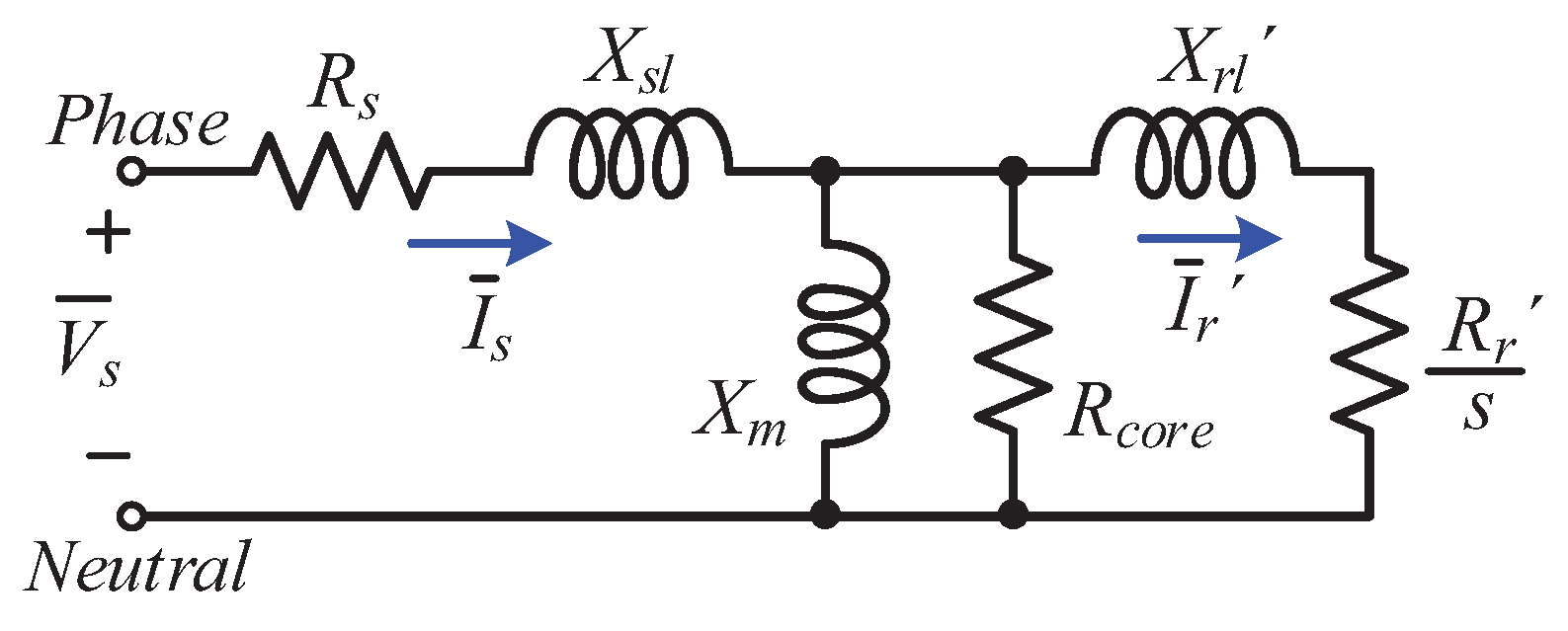
Figure 2.
High-frequency common mode model.
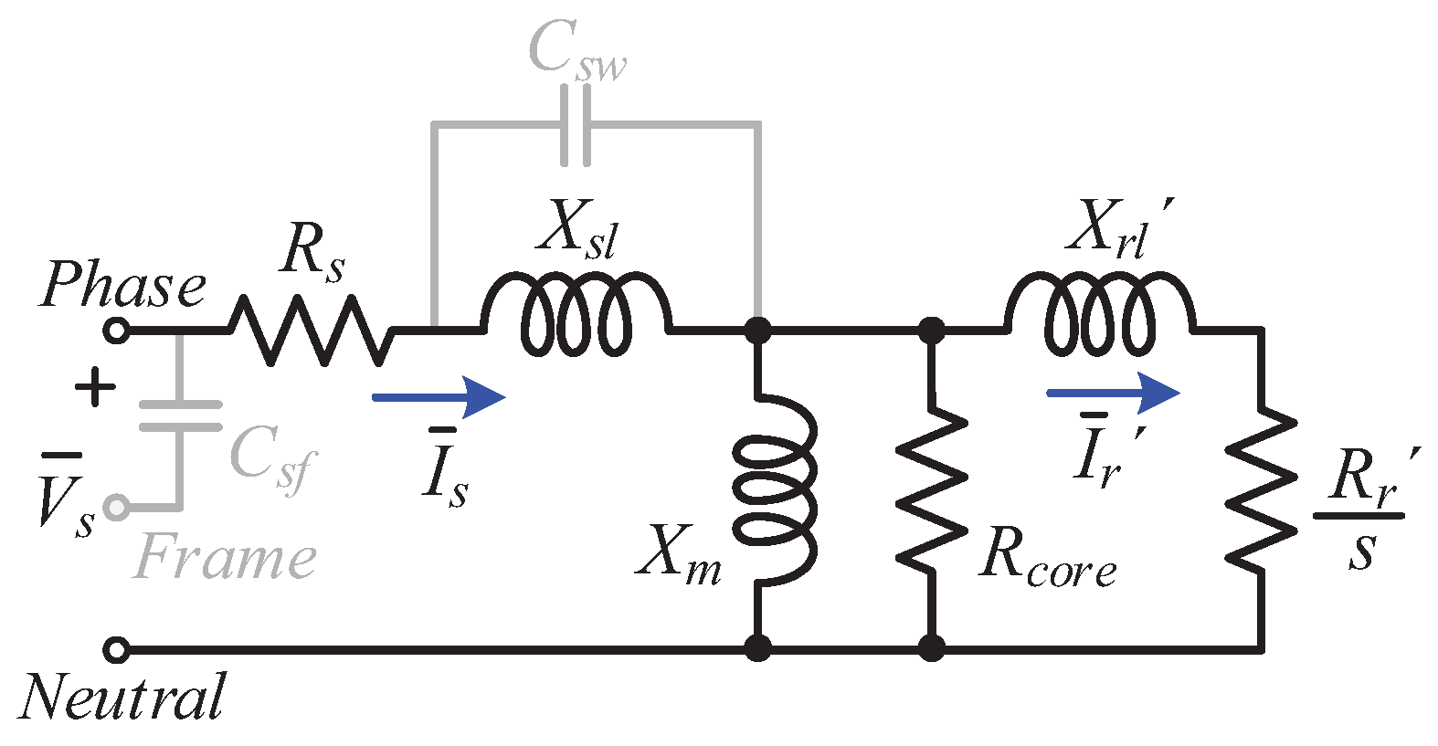
Figure 3.
Motor-bearing model.
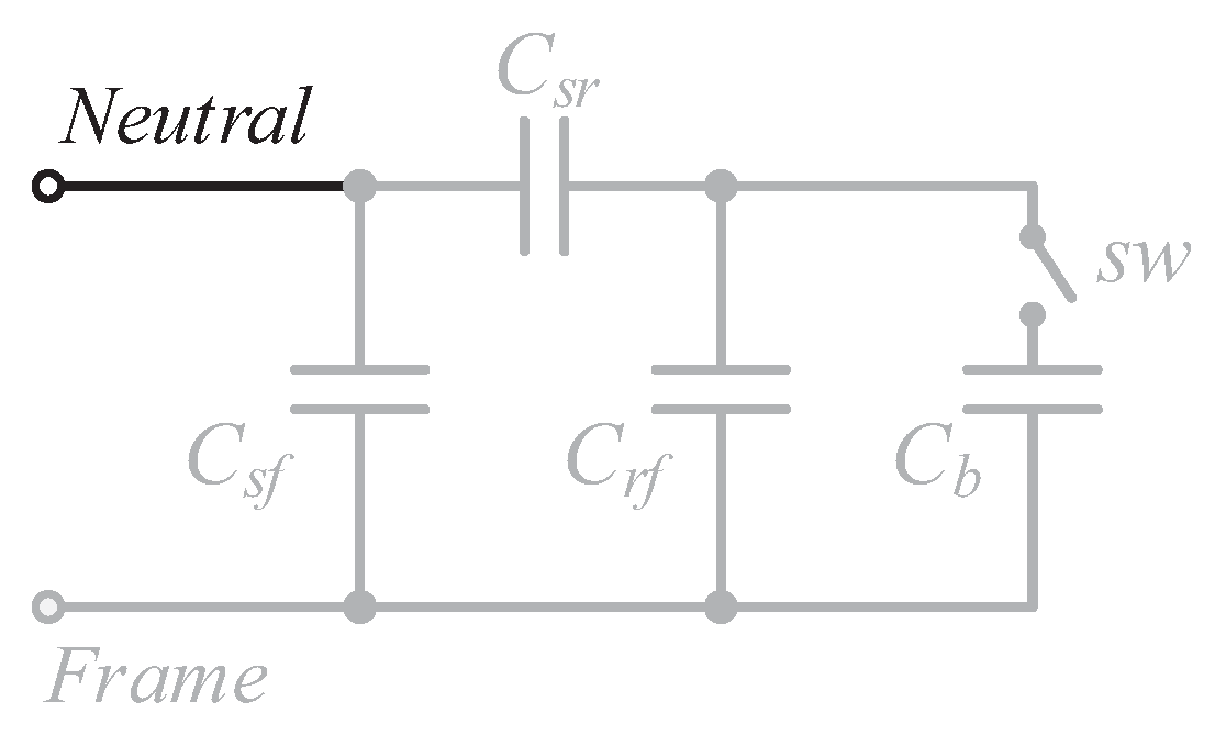
Figure 4.
Inverter topology to reduce leakage ground current in three-phase induction machines.
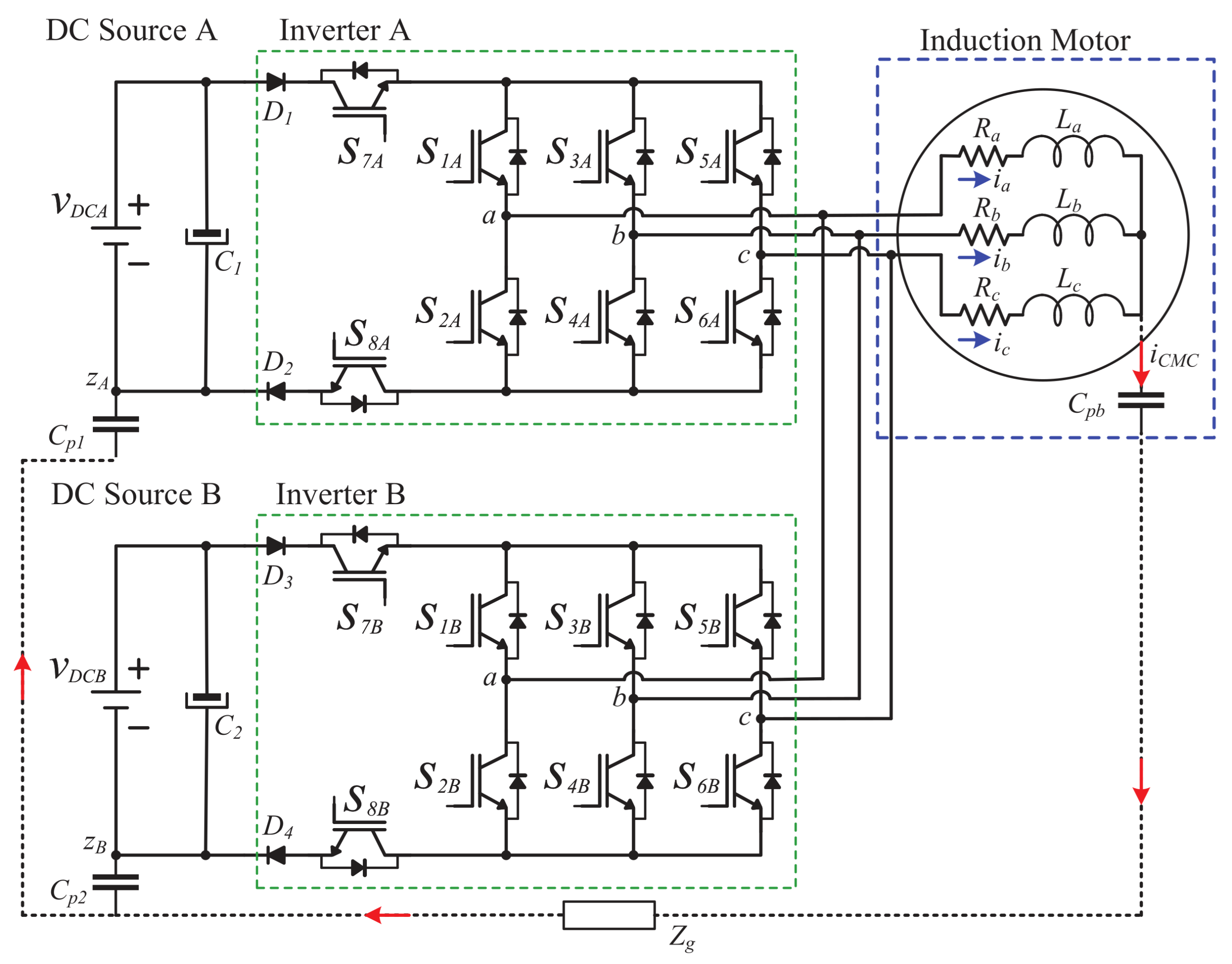
Figure 5.
Null state for the proposed inverter when is located at Sector I.
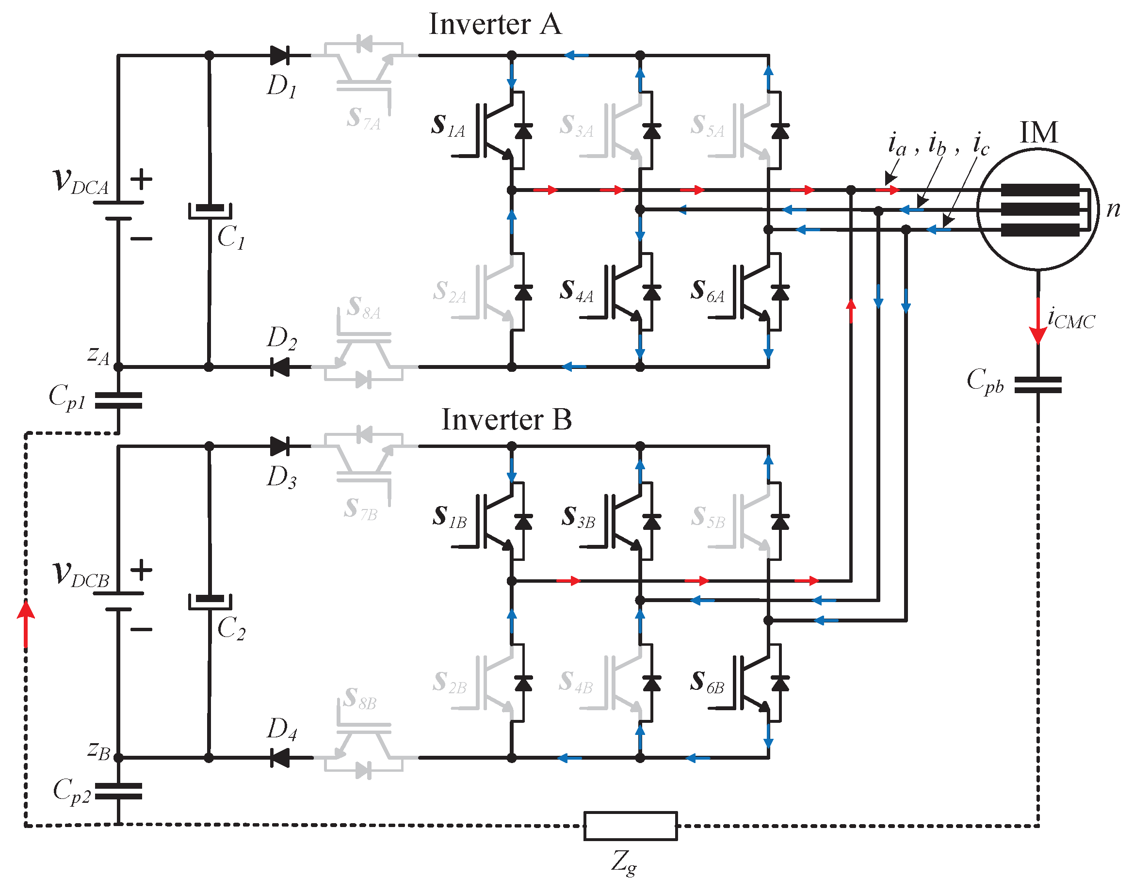
Figure 6.
Space vectors along a grid period in a complex plain with located at Sector I.
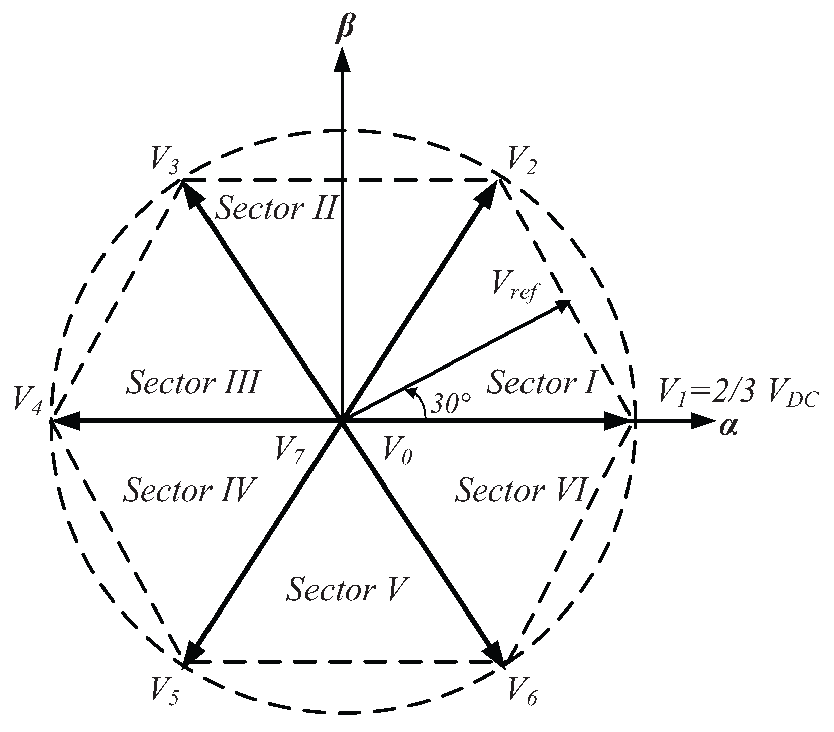
Figure 7.
Active state for the proposed inverter when is located at Sector I.
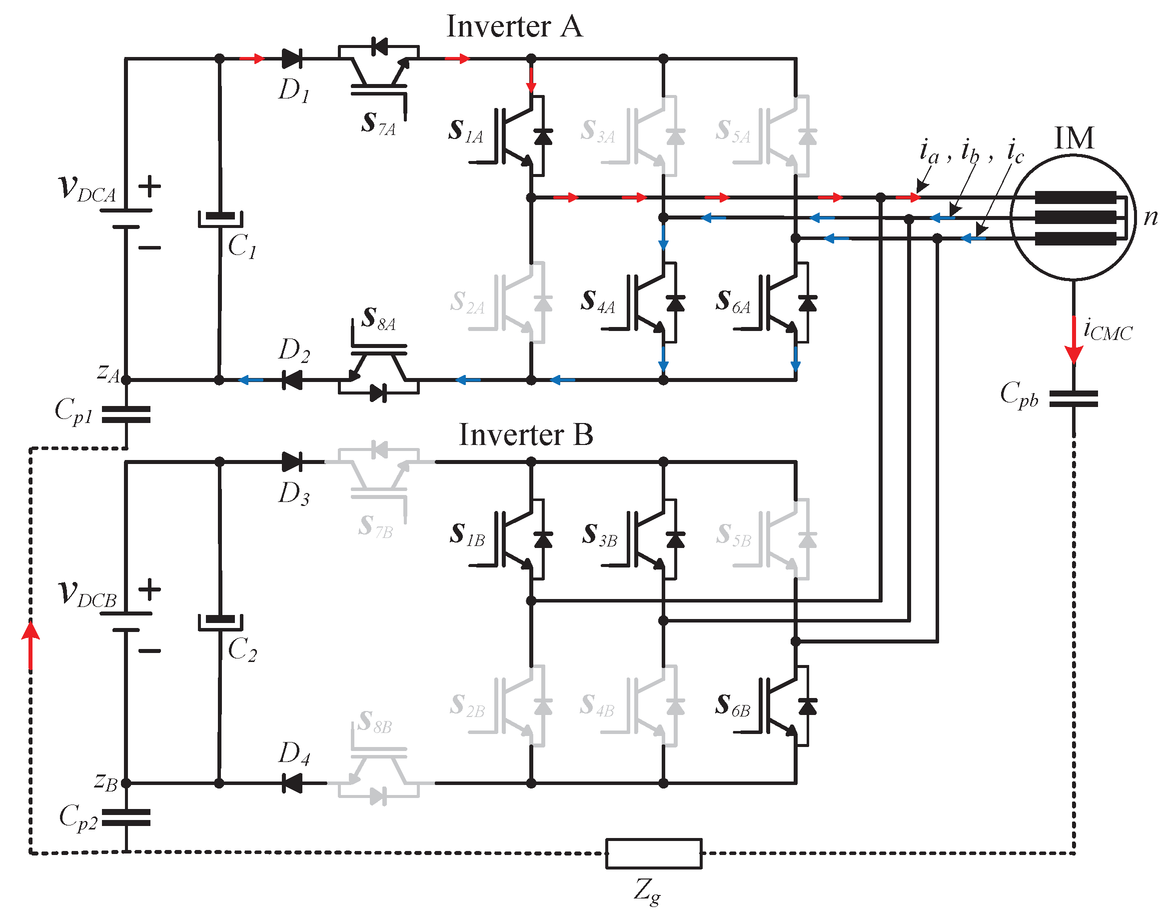
Figure 8.
Active state for the proposed inverter when is located at Sector I.
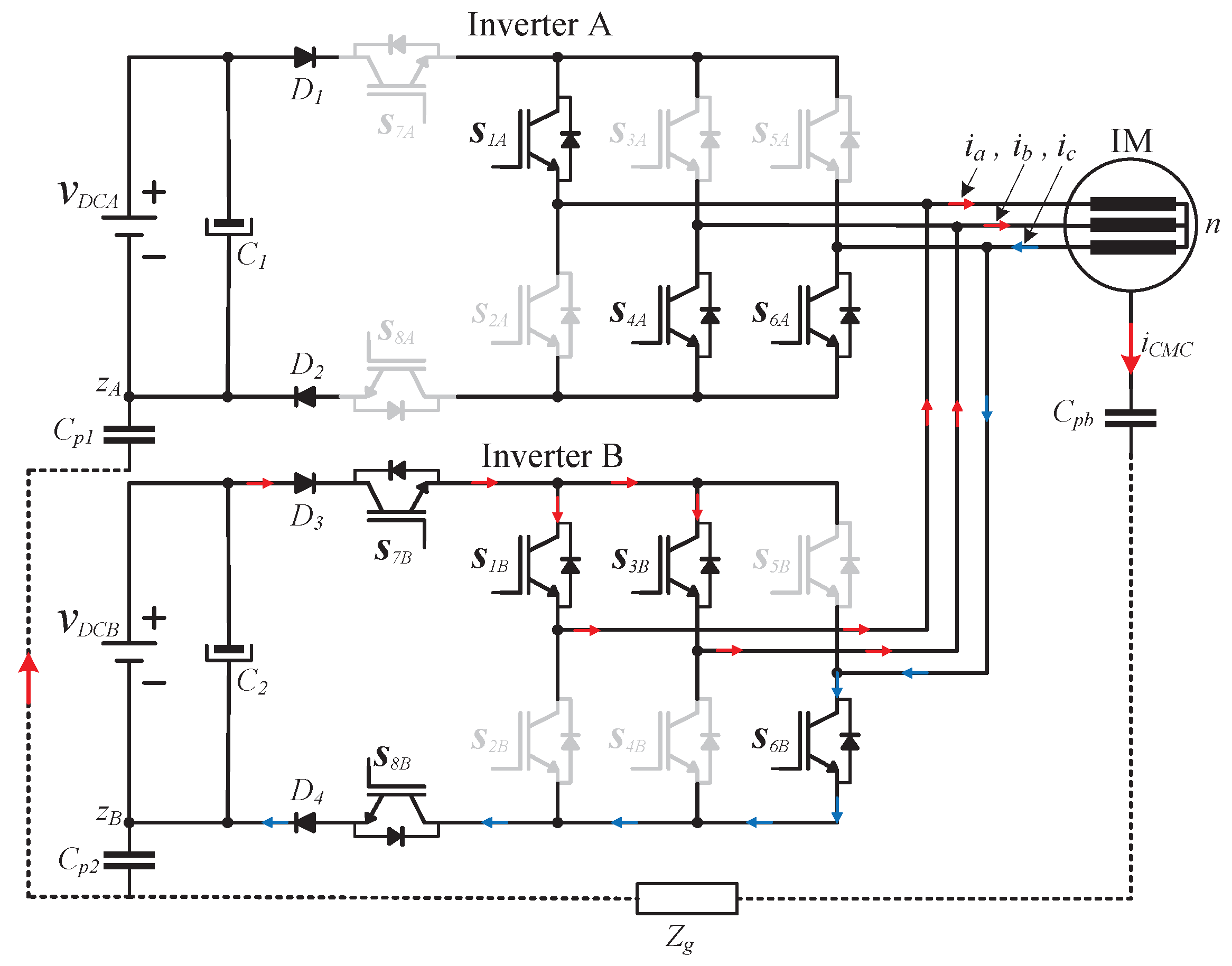
Figure 9.
Null state for the proposed inverter when is located at Sector I.
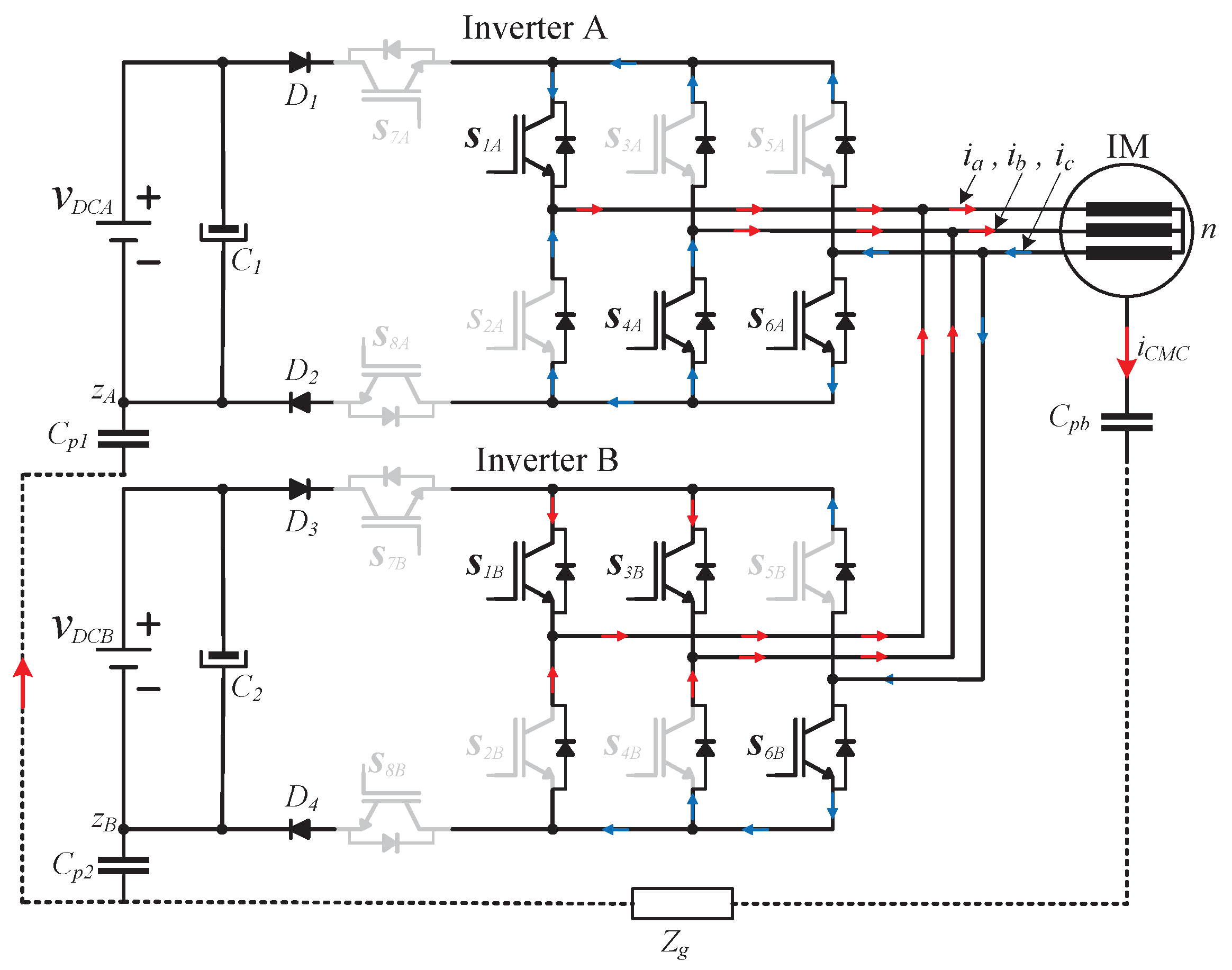
Figure 10.
Proposed space vector modulation sequence for Sector I in one switching period.
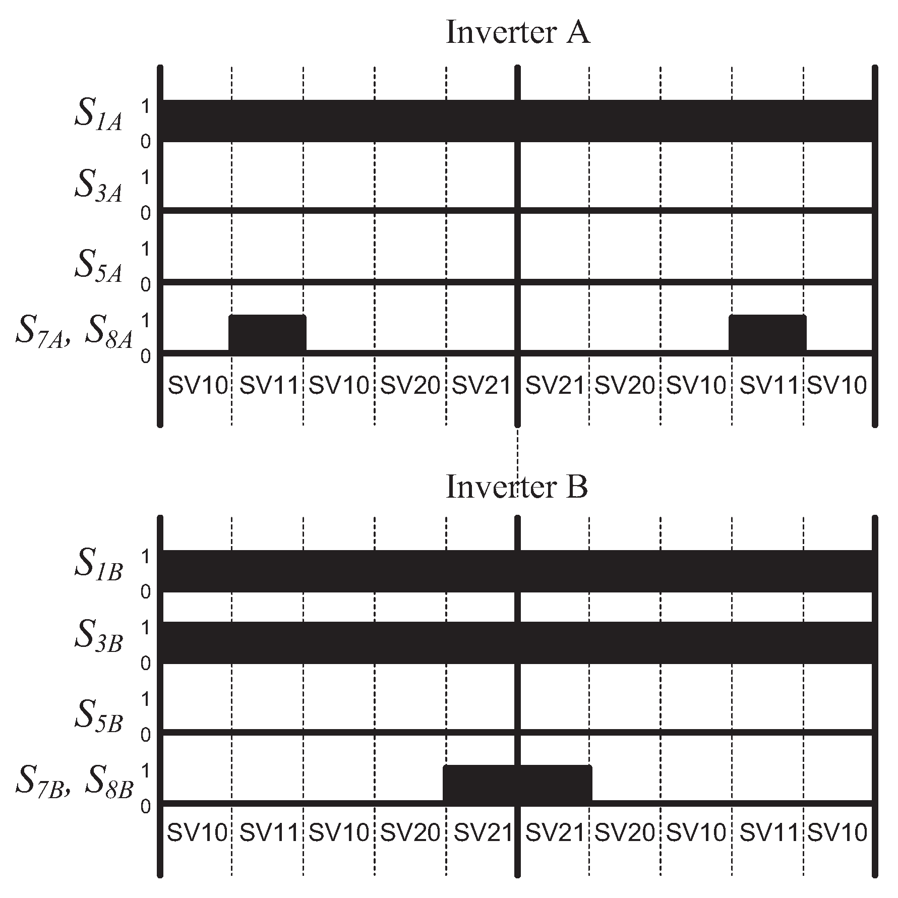
Figure 11.
Proposed switching pattern and evolution of Sectors along a grid period.
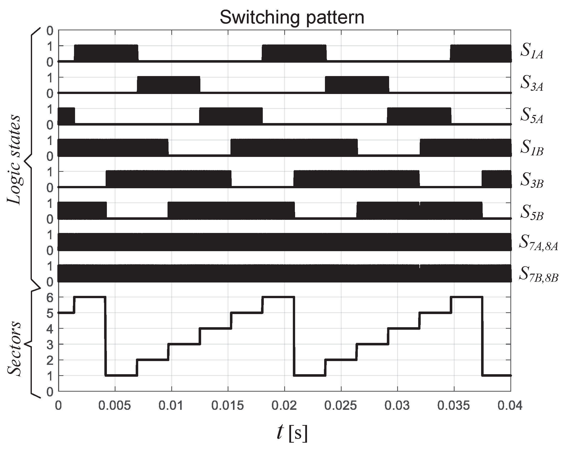
Figure 12.
(From top to bottom) Steady-state response of output currents (, , ), and leakage ground current ().
Figure 12.
(From top to bottom) Steady-state response of output currents (, , ), and leakage ground current ().
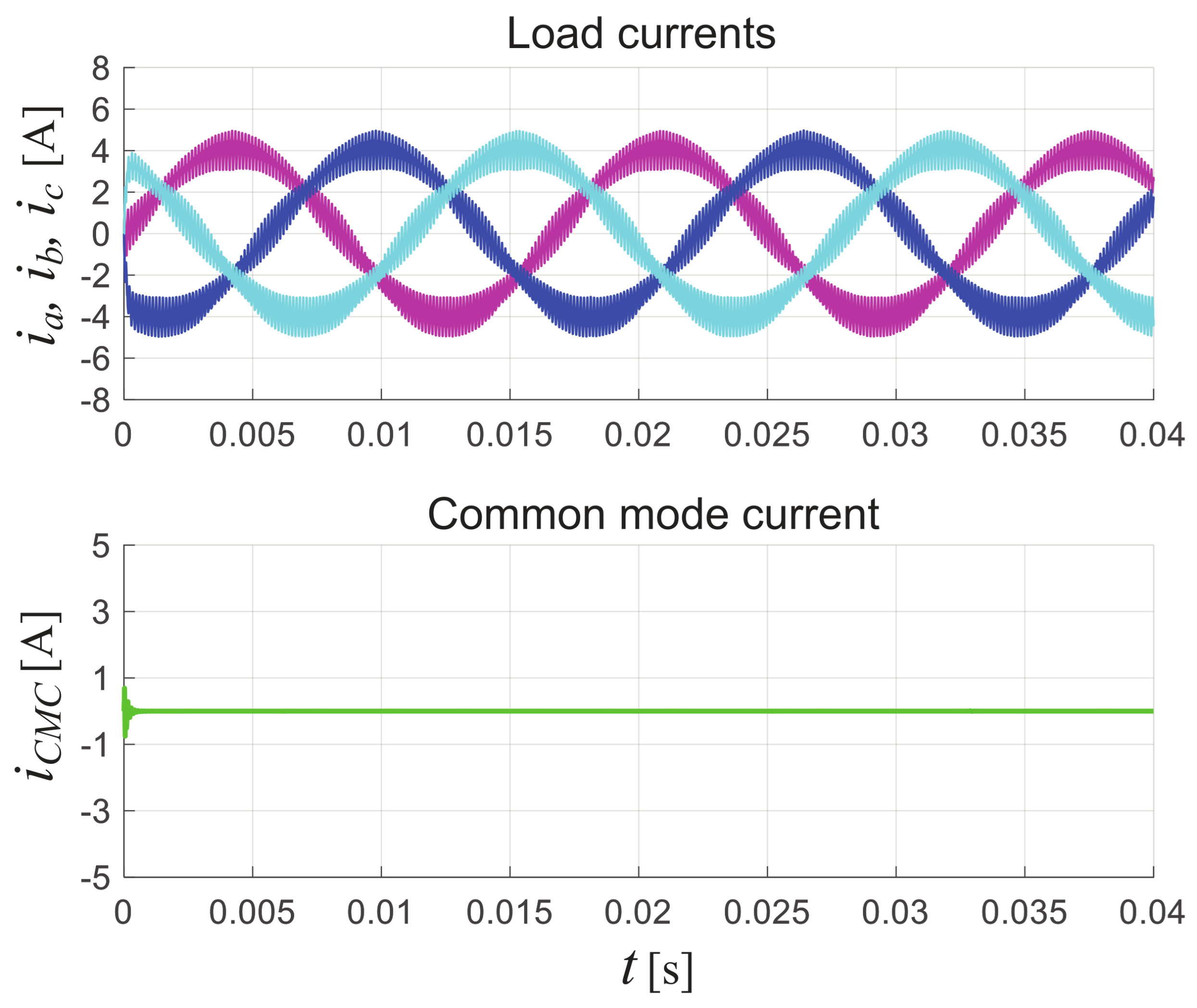
Figure 13.
(From top to bottom) Steady-state response of output line voltages (, , ).
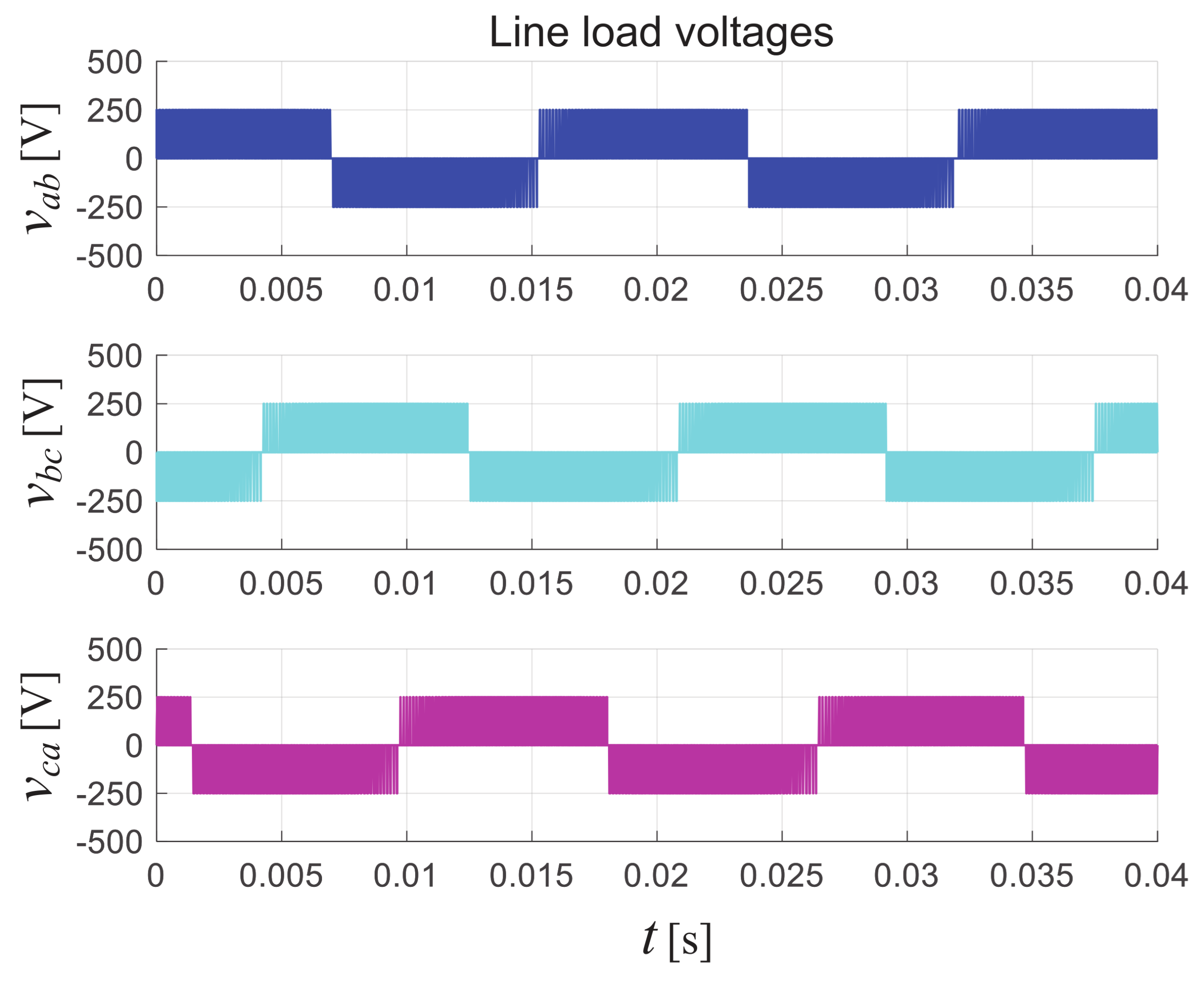
Figure 14.
(From top to bottom) Steady-state response of parasitic capacitor voltages, , , and common ground current, .
Figure 14.
(From top to bottom) Steady-state response of parasitic capacitor voltages, , , and common ground current, .
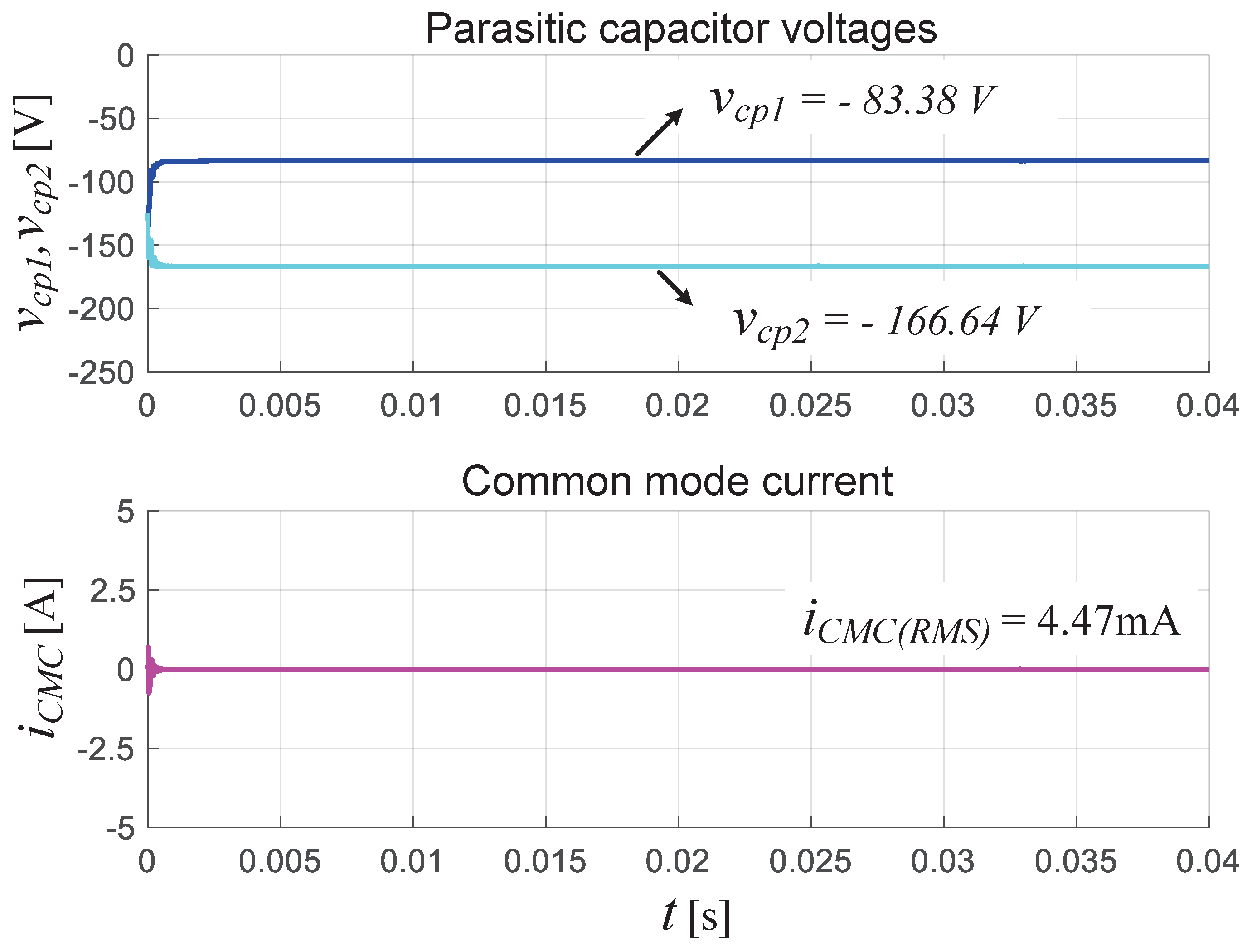
Figure 15.
(From top to bottom) transient response of output currents, , , , and common ground current, .
Figure 15.
(From top to bottom) transient response of output currents, , , , and common ground current, .
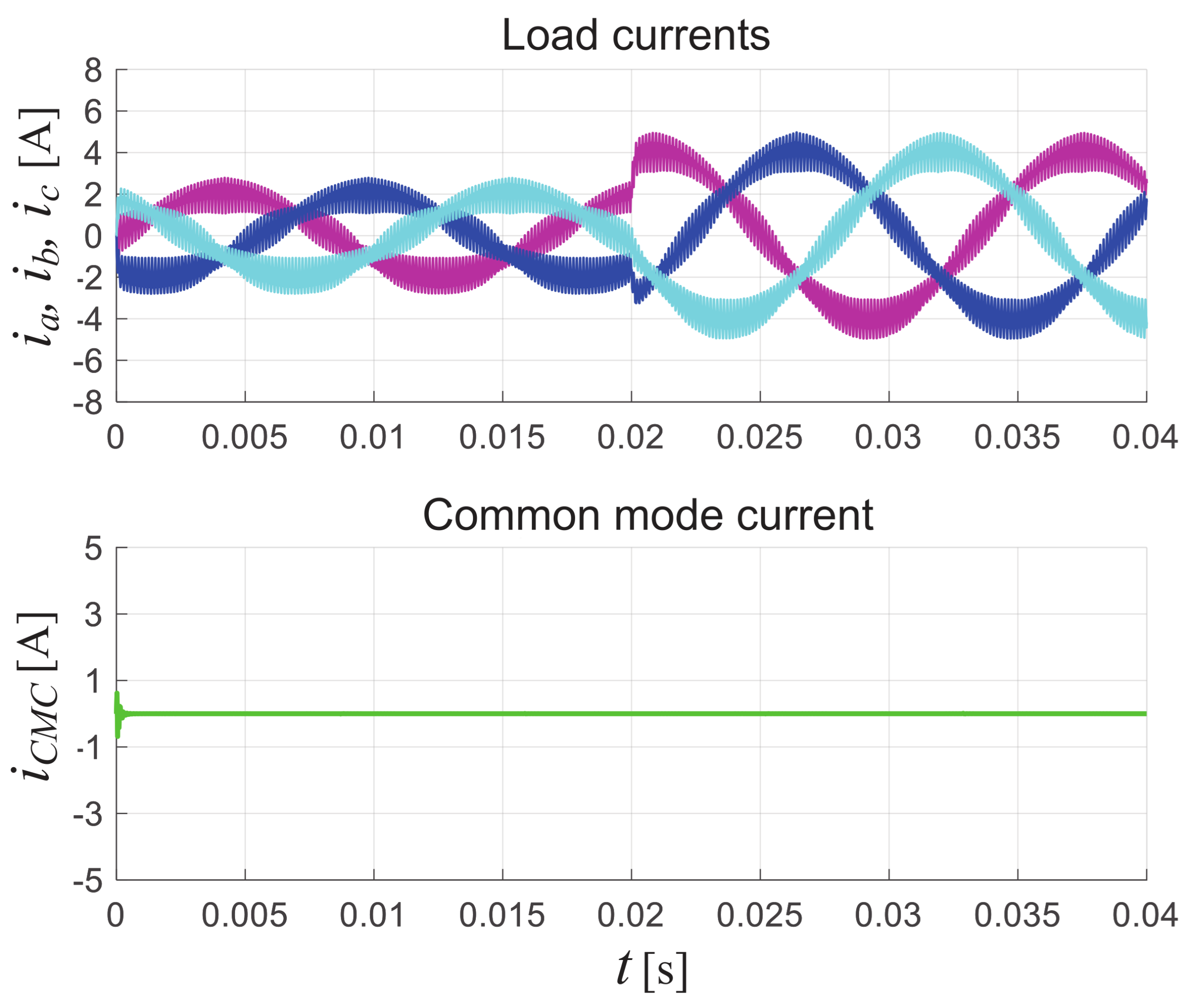
Figure 16.
(From top to bottom) Space vector modulation sequence.
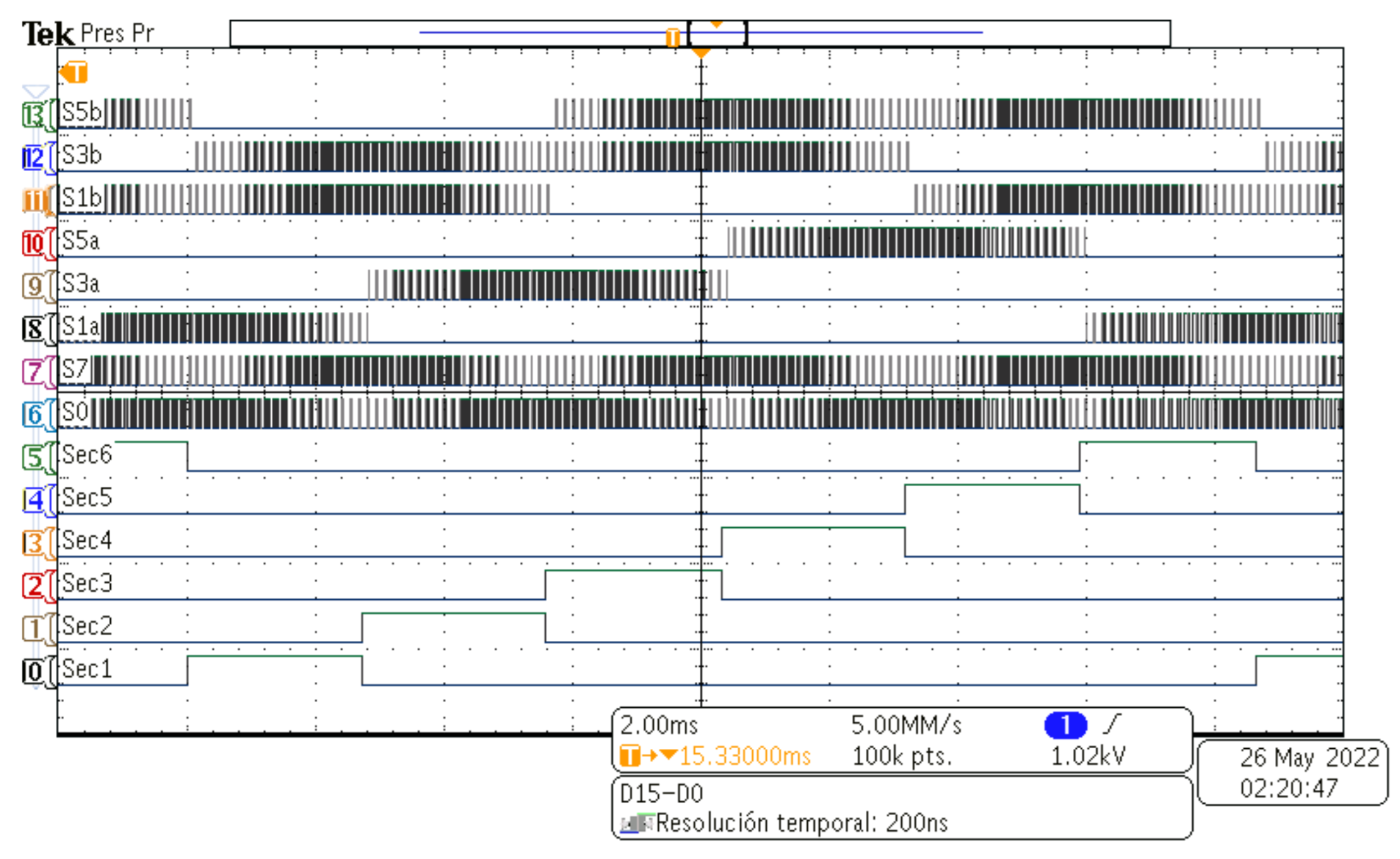
Figure 17.
(From top to bottom) Steady-state response of outputs currents (, , ), and leakage ground current ().
Figure 17.
(From top to bottom) Steady-state response of outputs currents (, , ), and leakage ground current ().
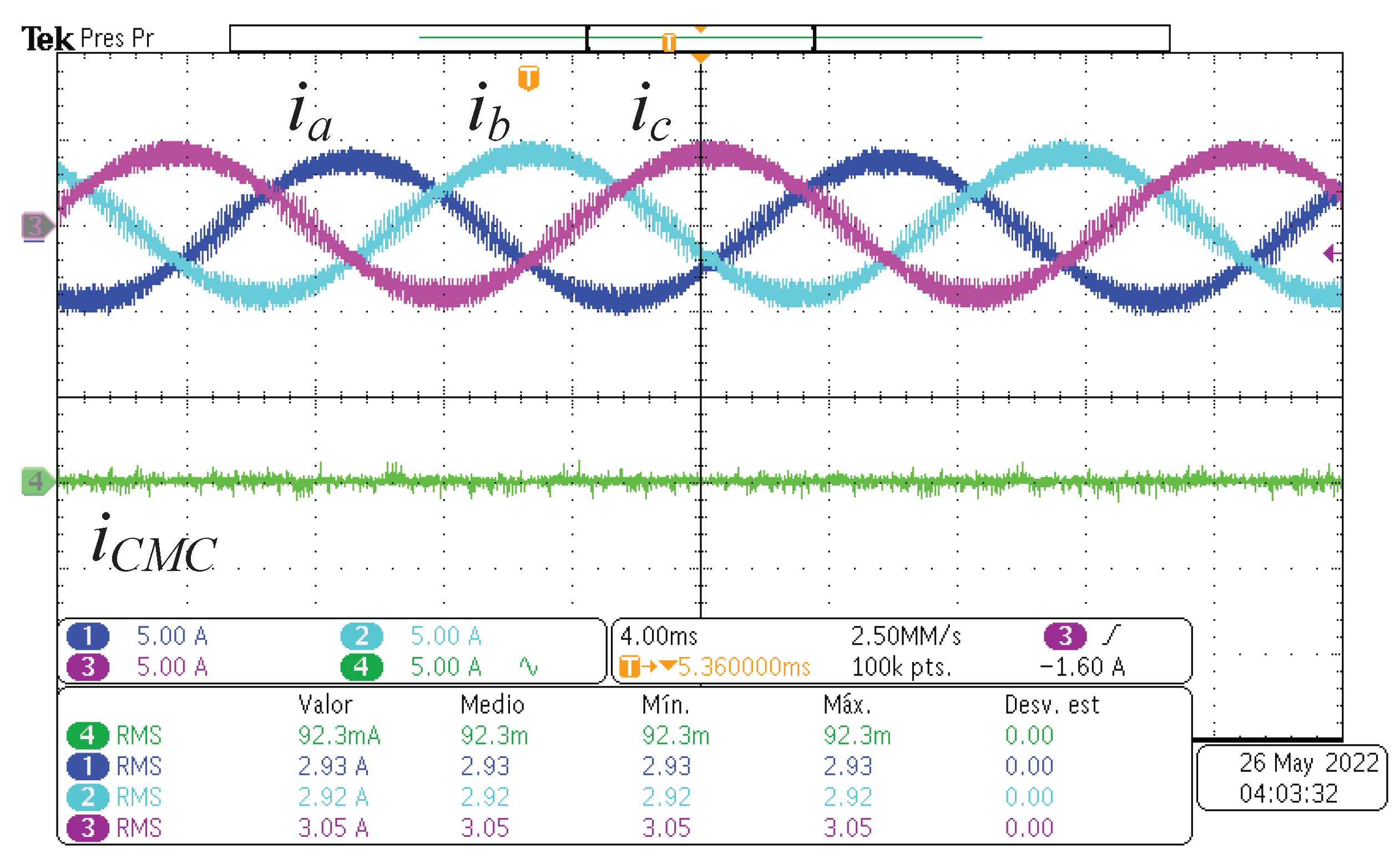
Figure 18.
(From top to bottom) Steady-state response of line-to-line voltages (, , ), and leakage ground current ().
Figure 18.
(From top to bottom) Steady-state response of line-to-line voltages (, , ), and leakage ground current ().
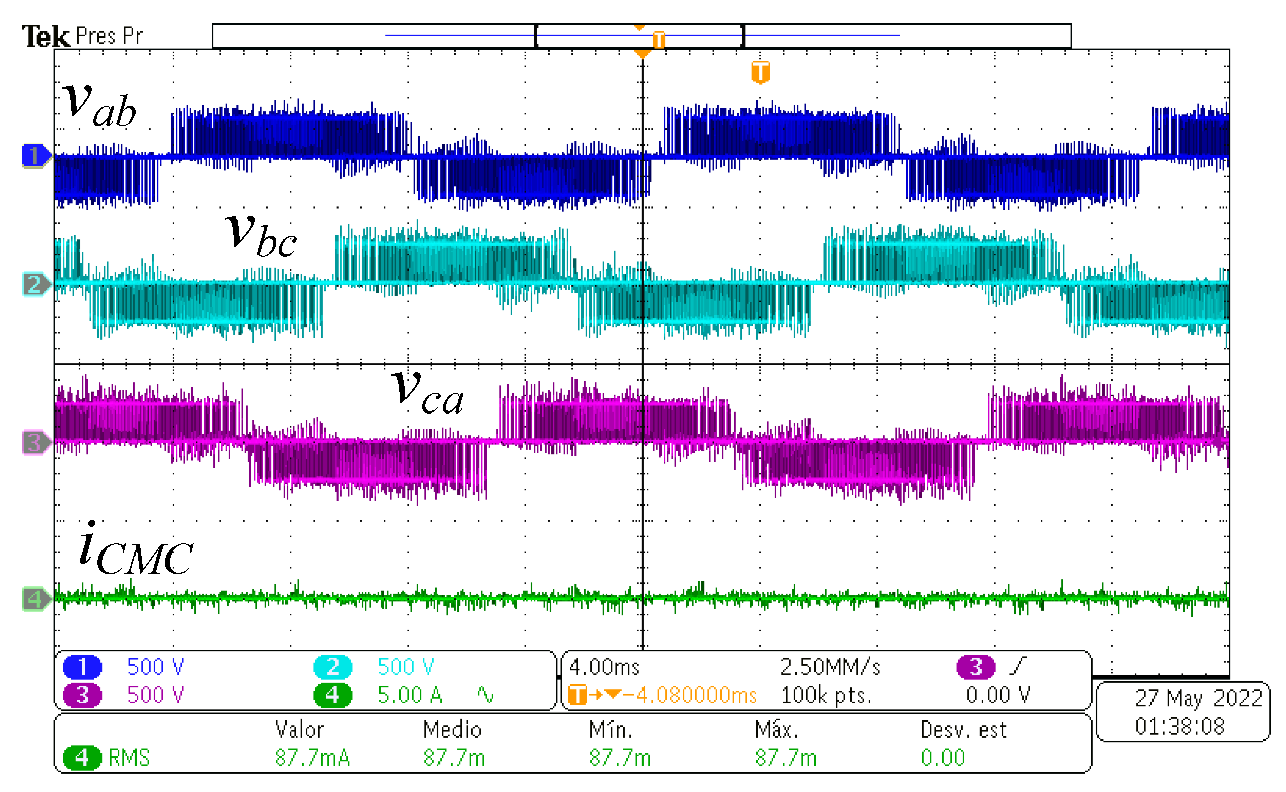
Figure 19.
(From top to bottom) Steady-state response of capacitor voltages (, ), and leakage ground current ().
Figure 19.
(From top to bottom) Steady-state response of capacitor voltages (, ), and leakage ground current ().
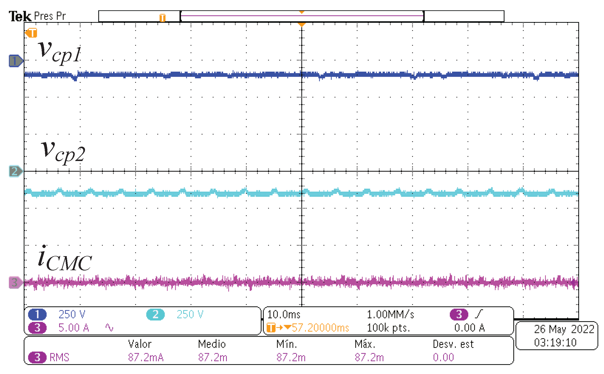
Figure 20.
(From top to bottom) Transient response of output currents (, , ) and ground leakage current (), under step load changes from 100% to 50%.
Figure 20.
(From top to bottom) Transient response of output currents (, , ) and ground leakage current (), under step load changes from 100% to 50%.
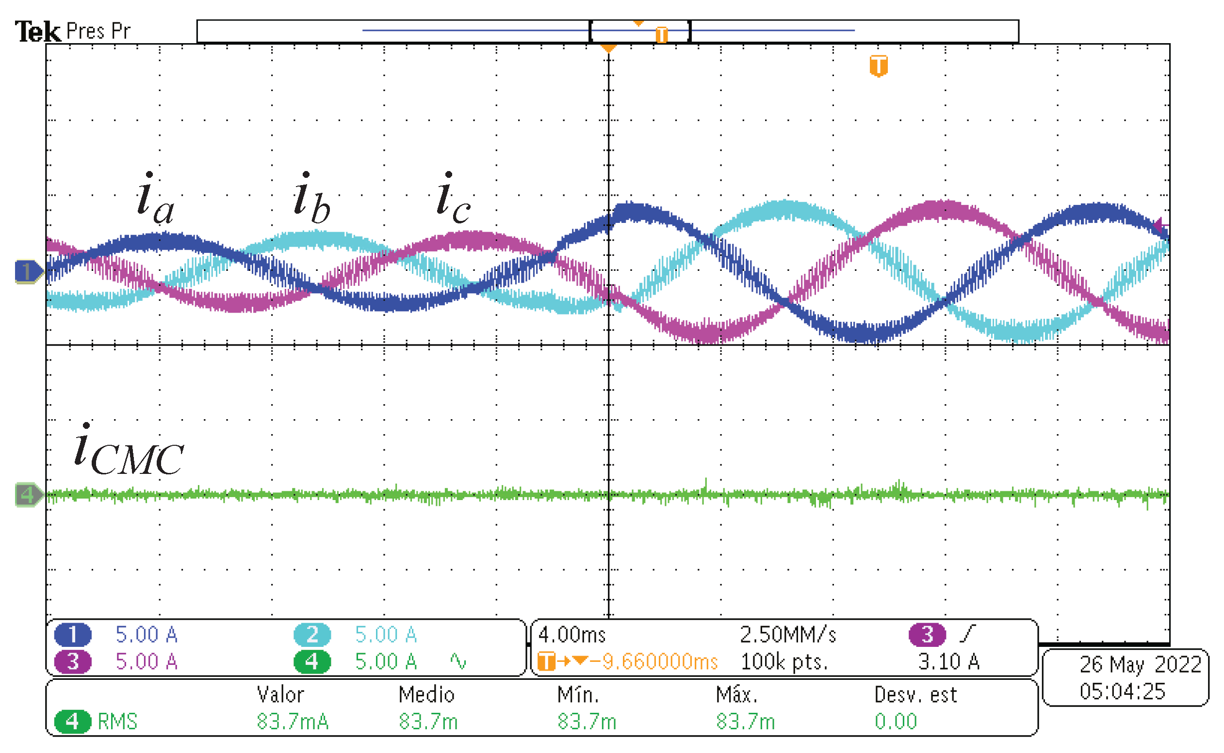

Table 1.
Inverter modulation states along Sector 1.
| State | ||||||||
|---|---|---|---|---|---|---|---|---|
| 1 | 1 | 0 | 0 | 1 | 1 | 0 | 0 | 0 |
| 2 | 1 | 0 | 0 | 1 | 1 | 0 | 1 | 0 |
| 3 | 1 | 0 | 0 | 1 | 1 | 0 | 0 | 1 |
| 4 | 1 | 0 | 0 | 1 | 1 | 0 | 0 | 0 |
Table 2.
Simulation and experimental parameters.
| Parameter | Value | Parameter | Value/Part number |
|---|---|---|---|
| 10 | |||
| , , | 25 | ||
| and | 7.7 kHz | ||
| , , | 2 mH | 60 Hz | |
| 160 nF | DIODES/IGBTs | STTH200R04TV/SKM50GB12T4 |
Disclaimer/Publisher’s Note: The statements, opinions and data contained in all publications are solely those of the individual author(s) and contributor(s) and not of MDPI and/or the editor(s). MDPI and/or the editor(s) disclaim responsibility for any injury to people or property resulting from any ideas, methods, instructions or products referred to in the content. |
© 2025 by the authors. Licensee MDPI, Basel, Switzerland. This article is an open access article distributed under the terms and conditions of the Creative Commons Attribution (CC BY) license (http://creativecommons.org/licenses/by/4.0/).
Copyright: This open access article is published under a Creative Commons CC BY 4.0 license, which permit the free download, distribution, and reuse, provided that the author and preprint are cited in any reuse.


