Submitted:
14 August 2025
Posted:
15 August 2025
You are already at the latest version
Abstract
To meet the needs of wearable devices and flexible electronic skin for curved, flexible temperature sensors, this paper presents a high-reliability flexible hybrid-integrated temperature sensor. Its core includes a CMOS sensor chip with an integrated bandgap reference circuit and dual-path ESD protection. The sensor achieves a low temperature drift of 20 ppm/℃ and 0.99% linearity from -40℃ to 125℃. After flexible integration and 100 bending cycles at a 10 mm radius, the reference voltage varies less than 0.1%, and temperature output shifts less than ±0.5℃. Temperature tests show an accuracy within ±1℃ across the full range, providing a precise and mechanically robust temperature monitoring solution.
Keywords:
Flexible temperature sensor
; CMOS sensing die
; Bandgap reference circuit
; wearable devices
; flexible electronic skin
2 College of Electrical Engineering, Zhejiang University, Hangzhou 310058, China
1. Introduction
In fields such as wearable health monitoring [1,2], electronic skin [3,4], and robotic sensing [5,6,7], there is an urgent need for high-precision, real-time temperature sensing that can conform closely to the human body or complex curved surfaces [8,9,10]. Applications include monitoring surface body temperature distribution, human-machine interaction thermal feedback, and battery thermal safety management [11]. Among mainstream flexible solutions, metal thin films (such as Pt, Ni) directly fabricated on flexible substrates can achieve relatively high sensing accuracy but suffer from low process maturity and high cost [12]. Carbon-based materials (such as graphene, carbon nanotubes) or organic semiconductors [13] directly built on flexible substrates offer advantages of good flexibility and stretchability but face challenges in maintaining linearity and long-term stability over a wide temperature range [14,15]. Hybrid integration of chips using flexible printed circuit boards (FPC) enables the direct use of mature CMOS integrated circuits while ensuring curved conformability of flexible sensing units [16,17].
Integrated circuit temperature sensing technology mainly relies on the temperature characteristics of silicon semiconductor PN junctions [18]. It uses the negative correlation between the base-emitter voltage (VBE) of bipolar transistors and temperature [19]. A bandgap reference circuit weights and sums VBE with a positive temperature coefficient voltage to generate a near-zero temperature drift reference voltage, which is then converted into a voltage output proportional to absolute temperature (PTAT). This method depends on the device layout matching of CMOS processes, but the core circuits are highly sensitive to stress interference, temperature drift, and electrostatic discharge [20].
2. Design and Fabrication
As shown in Figure 1, the die generates a zero-temperature-drift reference voltage with a bandgap reference circuit as the core. Internally, a bipolar transistor’s ΔVBE drives the PTAT circuit to produce a positive temperature coefficient current, which is then proportionally combined with a CTAT (negative temperature coefficient) current in the zero-temperature-drift synthesis circuit to output a nearly zero-temperature-drift reference voltage signal. This signal is buffered through a buffer circuit and output from the VREF pin, ensuring strong load interference immunity. The PTAT circuit of the bandgap reference is directly buffered by a buffer circuit and output from the TEMP pin, providing a highly linear temperature sensing voltage signal. A dual-path ESD protection network covers all pins; a clamp structure is used between VDD and GND, and a secondary discharge path is added at the TEMP and VREF pins, forming full-domain electrostatic protection. The four pins have clear functions: VDD for power supply (4.5–5.5 V), GND for ground, TEMP outputs the temperature voltage, and VREF provides the reference voltage, achieving integrated sensing, referencing, and protection.
The circuit schematic of the sensing die is shown in Figure 2(a). From left to right, it sequentially integrates a soft-start circuit (to suppress power surge impact), a bandgap reference core, a VBG circuit combining PTAT/CTAT currents, and a buffer amplifier circuit (implementing voltage proportional amplification through a resistor feedback network, respectively driving the reference output VREF and the temperature signal TEMP).
To raise the bias voltage and achieve layout matching, the parallel count ratio of Q1 to Q2 is selected as 16:2. The voltage division on resistor R1 in the bandgap reference core is expressed as follows [21]:
where represents the voltage difference between the base and emitter of the transistors. According to the current mirror current replication relationship, the following holds in the PTAT/CTAT fusion circuit [22]:
where I_PTAT is the PTAT current generated by the bandgap reference core, copied to branch Q3 through a current mirror, forming a PTAT voltage across resistor R2. The transistor Q3 provides the CTAT voltage. By adjusting the ratio between R1 and R2, the first-order temperature coefficient of VBG can be corrected. The output reference voltage is given by [23]:
The resistor ratio circuit constructed by OPA2 enables the VREF pin to have both strong driving capability and high input impedance, without affecting the voltage value of the VBG circuit. The temperature sensing pin is expressed as [24]:
where I_PTAT is the PTAT current generated by the bandgap reference core and copied via a current mirror to the R5 branch, forming a PTAT voltage across resistor R5. Additionally, because the resistor ratio circuit is constructed by OPA3, the TEMP pin possesses both large driving capability and high input impedance.
Figure 2(b) illustrates the ESD protection paths for the I/O pins such as VREF and TEMP, adopting a PMOS-NMOS bidirectional discharge structure (PMOS discharges towards the power supply, NMOS discharges towards ground), with a secondary NMOS discharge plus current-limiting resistor introduced to enhance transient response robustness. Figure 2(c) shows the ESD protection path for the power pins; VDD is directly connected to a large-size NMOS discharge transistor to ground, with a gate-integrated current-limiting resistor to prevent false triggering. This architecture ensures an ESD protection capability exceeding 4 kV HBM from the circuit design perspective.
Circuit simulation verification based on the commercial 180nm CMOS process PDK shows that under a 5 V/μs power supply slew rate, Figure 3(a) confirms the bandgap reference core powers up normally with an overshoot of less than 5%. Loop stability analysis in Figure 3(b) sets the phase margin above 55°, ensuring no risk of oscillation. Figure 3(c) shows the typical temperature drift of the reference voltage is 20 ppm/°C over the range of -40 to 125°C. PVT and Monte Carlo simulations (Figure 3d,e) indicate the worst-case temperature drift is ≤ 45 ppm/°C, and the reference voltage deviation is less than 8 mV (3σ). Figure 3(f) further verifies the temperature sensing voltage linearity over the full temperature range, with the reference output voltage at 25°C being 0.83 V and sensitivity stable at 5 mV/°C. These simulation results provide critical parameter boundaries for system redundancy design, supporting layout optimization during chip fabrication to achieve both temperature drift suppression and enhanced robustness.
Figure 3.
Simulation analysis of the schematic based on the foundry PDK. (a) Transient timing simulation of the startup circuit; (b) Stability simulation of the bandgap reference core loop; (c) Relationship between bandgap reference voltage and temperature; (d) Distribution of the temperature coefficient of the bandgap reference voltage based on Monte Carlo simulation; (e) Distribution of the bandgap reference voltage based on Monte Carlo simulation; (f) Relationship between the output voltage at the temperature output pin and temperature.
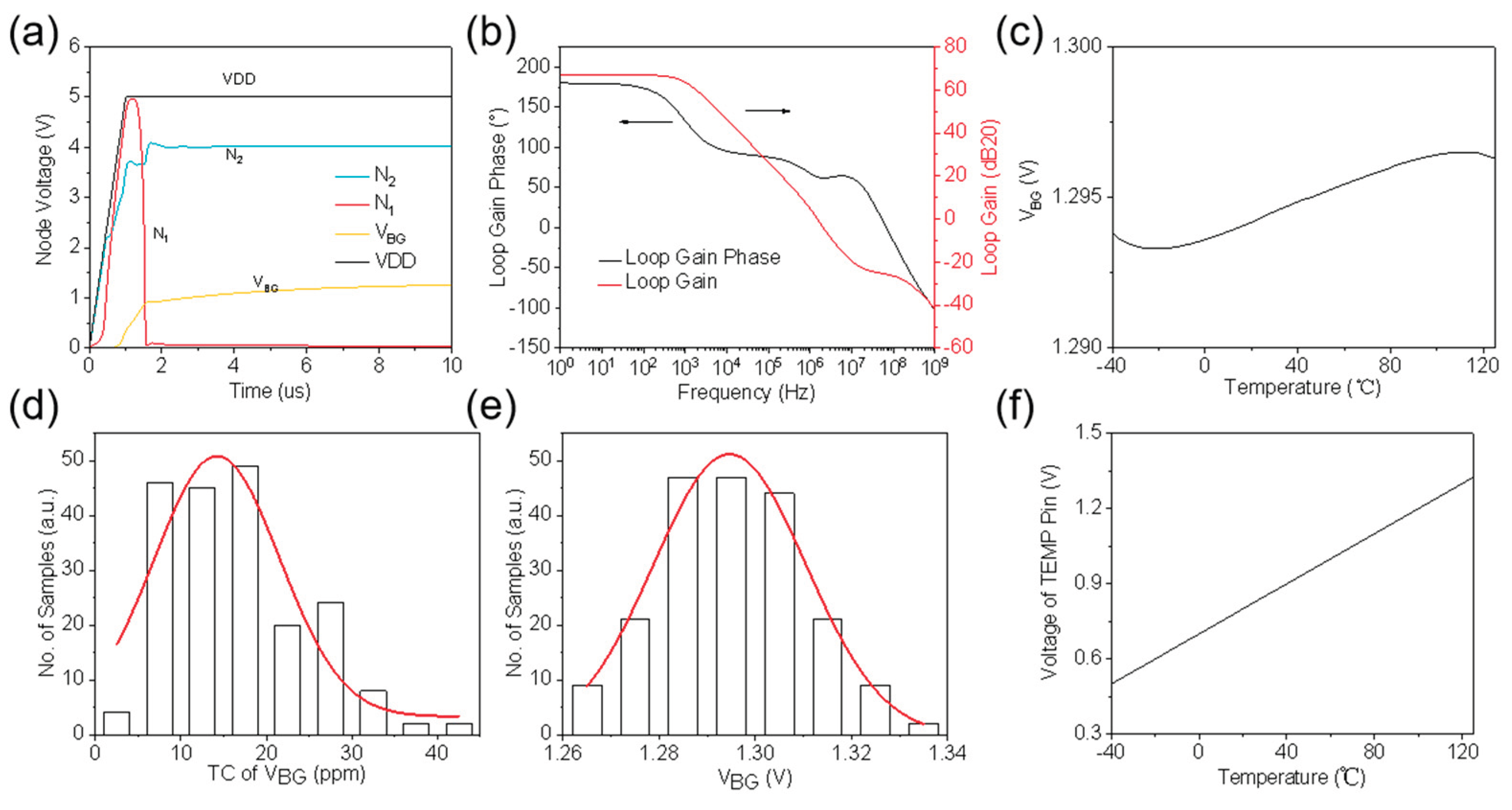
Figure 4.
Layout drawing based on the foundry PDK.
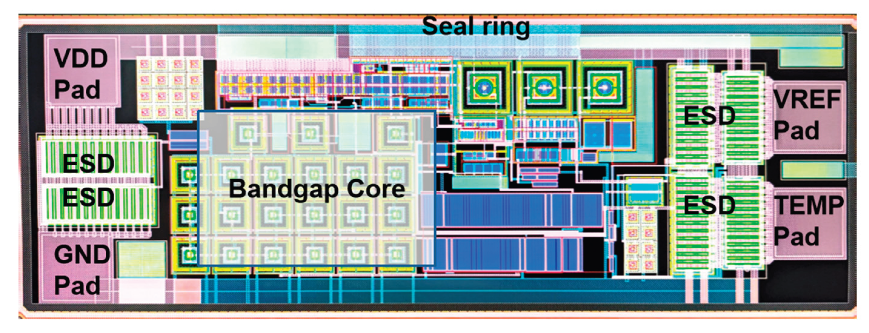
The layout strictly follows the 180 nm CMOS process design rules. The core area includes the bandgap reference source (occupying 0.08 mm², using common-centroid matched layout to suppress gradient errors), a dual-path ESD protection network (with large-size clamp transistors integrated at the VDD/GND pins, accounting for 22% of the area), and four aluminum-copper alloy pins (VDD/GND/TEMP/VREF, each with a width of 80 μm). The periphery is equipped with a double-layer seal ring structure (20 μm wide, deeply grounded region ring) to provide mechanical stress buffering. Key signal routing employs shielding protection (temperature sensing lines with 3 μm width and 2 μm spacing), and the reference voltage path is routed as differential symmetrical lines to reduce crosstalk. The entire layout has passed DRC/LVS verification with zero errors.
The fabrication process [25] of the flexible hybrid-integrated temperature sensor is shown in Figure 5(a). Based on a standardized process (FPC → die conductive epoxy mounting → gold wire bonding → PDMS encapsulation), high-precision integration of a 1.2 × 0.6 mm² CMOS sensing bare die with a flexible printed circuit board is achieved. A photograph of the flexible sensor is shown in Figure 5(b), and close-up photos of the gold wire bonding and encapsulation are shown in Figure 5(c). To minimize strain on the die during bending of the flexible device, the back of the die is polished to a thickness of 200 μm before assembly. As a result, the overall thickness of the flexible sensor is only 0.3 mm. Through finite element simulation modeling and analysis, at a bending radius of 10 mm, the maximum strain in the xx direction in the die area is less than 0.5%, and the strain at the bonding points in the xx direction is less than 3% (below the failure threshold), ensuring mechanical reliability of the bare die under dynamic deformation. The entire fabrication process relies on a mature fabless model, ensuring design reproducibility and mass production capability.
3. Results and Discussion
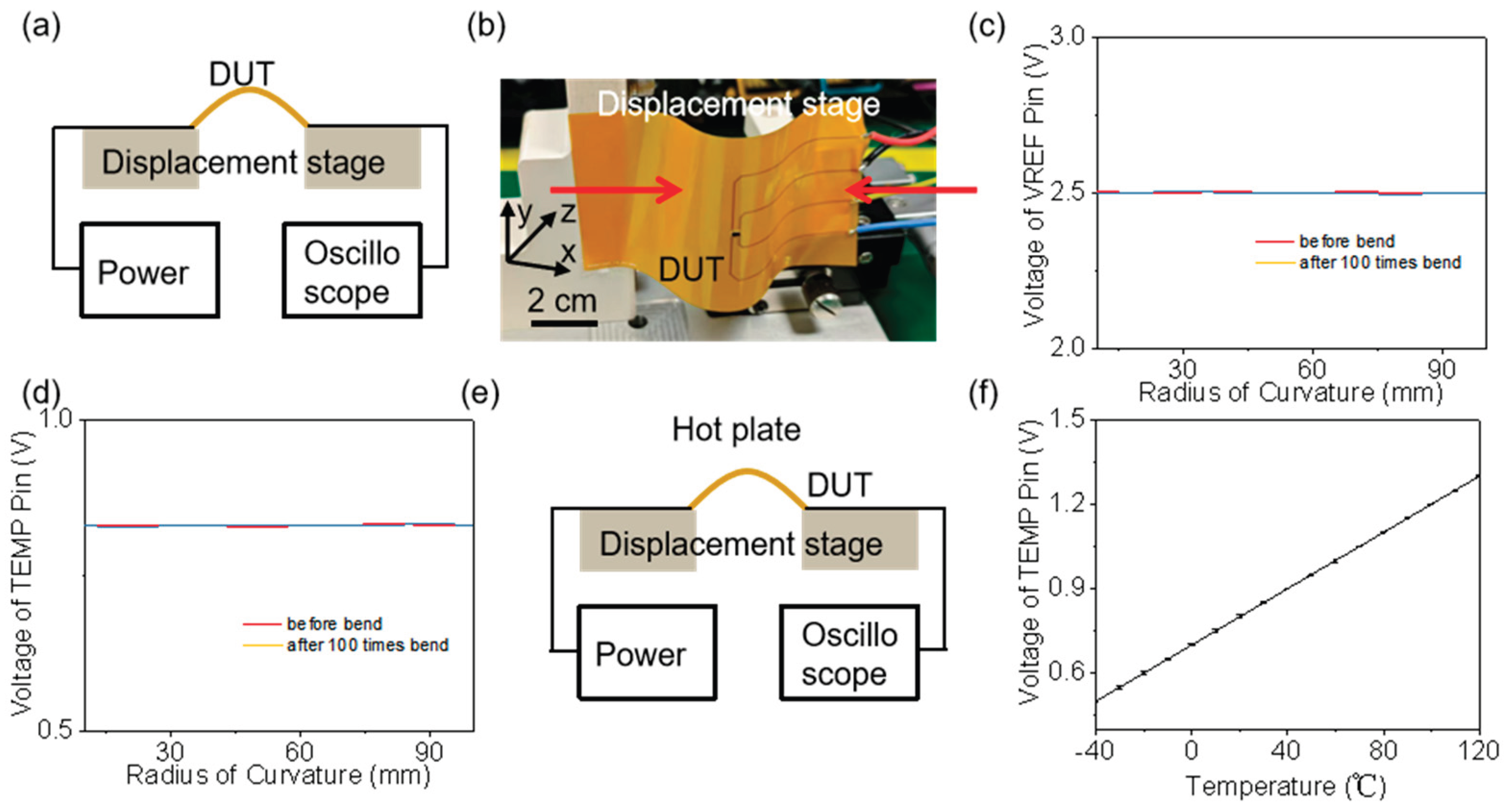
The testing setup is shown inFigure 6(a,b). A digital power supply provides adjustable voltage signals (1.8 V / 2.5 V / 3.3 V / 5 V), with the flexible device’s pins connected to the sensing die. An oscilloscope captures the output voltage’s time-domain signal, and a multimeter monitors the static voltage, enabling verification of electrical characteristics. Both ends of the flexible device are mounted on a bidirectional displacement platform; displacement along the x-axis causes bending of the flexible device. A microscope is positioned along the y-axis to capture the device’s contour and determine the bending radius at the sensing die location.
The relationship between reference voltage output, temperature pin voltage output, and bending radius before bending and after 100 bending cycles of the flexible hybrid-integrated temperature sensor is shown in Figure 6(c,d). It can be observed that at bending radii above 10 mm, the slight strain endured by the die does not alter the electrical performance of the reference and temperature outputs, indicating the flexible device has strong mechanical stability. Figure 6(e) is a schematic of the experimental setup for testing the temperature drift characteristics of the flexible device. A hot plate is used to change the temperature at the die’s location; after stabilizing for 20 minutes, the temperature pin voltage output is recorded. The results, shown in Figure 6(f), indicate an output voltage of 0.825 V at 25°C, with sensitivity stable at 5.0 mV/°C and linearity of 0.99%. This demonstrates that the temperature sensor has an output offset of less than ±0.5°C and a full-temperature-range testing accuracy error stable within ±1°C. Additionally, five samples underwent ESD testing (HBM, CDM, MM); all pins withstood electrostatic discharge stresses of HBM/4 kV, CDM/500 V, and MM/200 V.
4. Conclusions
In summary, this paper presents a highly reliable flexible hybrid-integrated temperature sensor based on a customized CMOS sensing die. Through the collaborative design of the bandgap reference circuit and dual-path ESD protection within the die, a low temperature drift coefficient of 20 ppm/°C and a linearity of 0.99% are achieved across a wide temperature range of -40 to 125°C. By combining bare-die-level flexible printed circuit (FPC) hybrid integration technology, the mechanical mismatch challenge between the rigid chip and flexible substrate is effectively overcome. Experimental results demonstrate that under 100 bending cycles at a 10 mm bending radius, the temperature output shift remains within ±0.5°C, and the full-temperature-range testing accuracy error is stabilized within ±1°C. All pins withstand electrostatic discharge stresses of HBM/4 kV, CDM/500 V, and MM/200 V. Compared with existing flexible temperature sensing solutions, this design achieves improvements in precision, reliability, and conformability simultaneously, providing a viable technical solution for wearable health monitoring, electronic skin, and dynamic thermal sensing in robotics.
Funding
This work was supported by the National Key Research and Development Program of China (2022YFB3207703) and the Key Research and Development Program of Ningbo (2023Z153).
Institutional Review Board Statement
Not applicable.
Informed Consent Statement
Not applicable.
Data Availability Statement
The data presented in this study are available upon request.
Acknowledgments
The authors thank School of Electrical Engineering at Southeast University, Ningbo CRRC Times Transducer Technology Co., Ltd. and the College of Electrical Engineering at Zhejiang University for facility support.
Conflicts of Interest
The authors declare no conflicts of interest.
References
- Deng Z Y, Guo L H, Chen X M. Smart wearable systems for health monitoring. Sens. 2023, 23, 2479.
- Yoon H, Park S H. A nontouchscreen tactile wearable interface as an alternative to touchscreen-based wearable devices. Sens. 2020, 20, 1275.
- Du Y C, Kim J H, Kong H. Biocompatible electronic skins for cardiovascular health monitoring. Adv. Healthcare Mater. 2024, 13, 03461.
- Oh J Y, Lee Y, Lee T. Skin mountable functional electronic materials for bio-integrated devices. Adv. Healthcare Mater. 2024, 13, 03797.
- Liu S Z, Guo W T, Chen H. Recent progress on flexible self-powered tactile sensing platforms for health monitoring and robotics. Small. 2024, 20, 240.
- Ma Z, Ding C, Li L. The design of decoupled robotic arm based on chain transmission. Mach. 2024, 12, 410. [Google Scholar] [CrossRef]
- Chen L, Zhao Y, Shen Y. 3D stitching double weave fabric-based elastic triboelectric nanogenerator for energy harvesting and self-powered sensing. energies. 2023, 16, 2284. [CrossRef]
- Hegde C, Su J T, Tan J M R. Sensing in soft robotics. ACS Nano. 2023, 17, 15277–15307.
- Jia X T, Guo R, Tay B K. Flexible ferroelectric devices: status and applications. Adv. Funct. Mater. 2022, 32, 2205933.
- Arora E K, Sharma V, Ravi A. Polyaniline-based ink for inkjet printing for supercapacitors, sensors, and electrochromic devices. energies. 2023, 16, 6716. [CrossRef]
- Dou W Q, Zhong G L, Cao J L. Soft robotic manipulators: designs, actuation, stiffness tuning, and sensing. Adv. Mater. Technol. 2021, 6, 2100018. [Google Scholar] [CrossRef]
- Hui Z Y, Zhang L R, Ren G Z. Green flexible electronics: natural materials, fabrication, and applications. Adv. Mater. 2023, 35, 841.
- Ji L, Shi J Q, Wei J. Air-stable organic radicals: new-generation materials for flexible electronics. Adv. Mater. 2020, 32, 1908015.
- Nair N M, Zumeit A, Dahiya R. Transparent and transient flexible electronics. Adv. Sci. 2025, 1, 100.
- Li D D, Lai W Y, Zhang Y Z. Printable transparent conductive films for flexible electronics. Adv. Mater. 2018, 30, 1704738.
- Ma Y, Zhang Y, Cai S. Flexible hybrid electronics for digital healthcare. Adv. Mater. 2020, 32, 1902062. [CrossRef]
- Borghetti M, Cantù E, Sardini E. Future sensors for smart objects by printing technologies in industry 4.0 scenario. energies. 2020, 13, 5916. [CrossRef]
- Zhang Z Y, Liang L, Wang L. Maximum chip temperature direct monitoring for press-pack IGBT integrating temperature sensors. IEEE Trans. Power Electron. 2025, 40, 8049–8061. [Google Scholar] [CrossRef]
- Chang J, Yin Y L, Du J H. On-chip integrated high-sensitivity temperature sensor based on p-GaN/AlGaN/GaN heterostructure. IEEE Electron Device Lett. 2023, 44, 594–597.
- Huang M M, Wu X Y, Zhao L B. Small-size temperature/high-pressure integrated sensor via flip-chip method. Microsyst. Nanoeng. 2024, 10, 104.
- Guo J M, Ma M H, Li Y Q. Bandgap engineering of ZrGaO films for deep-ultraviolet detection. IEEE Electron Device Lett. 2021, 42, 895–898.
- Hedayati R, Lanni L, Rusu A. Wide temperature range integrated bandgap voltage references in 4H-SiC. IEEE Electron Device Lett. 2016, 37, 146–149. [CrossRef]
- Butler P A, Waller W M, Uren M J. Ohmic contact-free mobility measurement in ultra-wide bandgap AlGaN/AlGaN devices. IEEE Electron Device Lett. 2018, 39, 55–58. [CrossRef]
- Zhu L Q, Wu T X, Wang Z H. Low dark current HgCdTe long wavelength infrared photodiodes with bandgap gradient multi-layer heterojunction. IEEE Electron Device Lett. 2024, 45, 797–800.
- Luo Y, Fang Y, Lv Y. Flexible hybrid integration hall angle sensor compatible with the CMOS process. Sens. 2025, 25, 927. [CrossRef]
Figure 1.
Circuit architecture diagram of the high-reliability temperature sensing die.
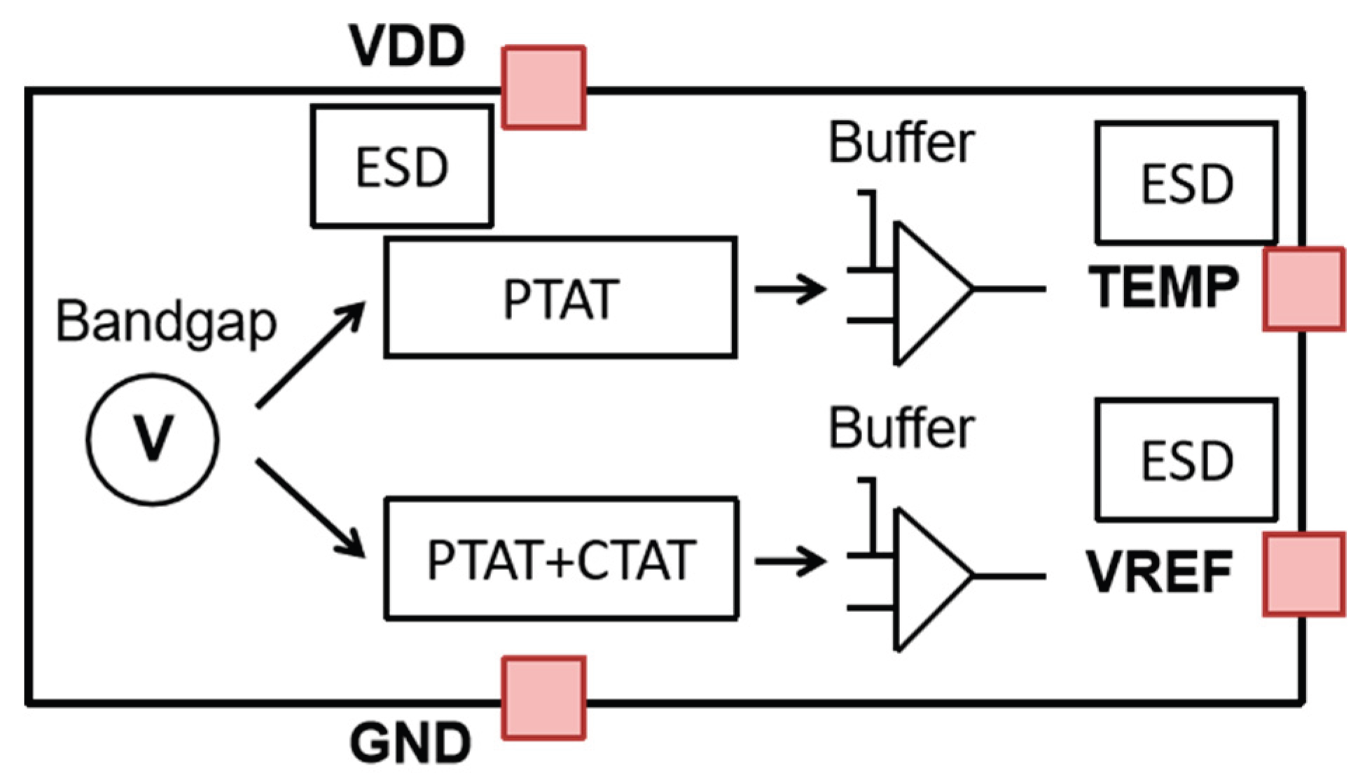
Figure 2.
Circuit schematic. (a) Schematic of the circuit generating the reference output and temperature sensing signals; (b) Schematic of the ESD protection path for the input/output pins; (c) Schematic of the ESD protection path for the power supply pins.
Figure 2.
Circuit schematic. (a) Schematic of the circuit generating the reference output and temperature sensing signals; (b) Schematic of the ESD protection path for the input/output pins; (c) Schematic of the ESD protection path for the power supply pins.
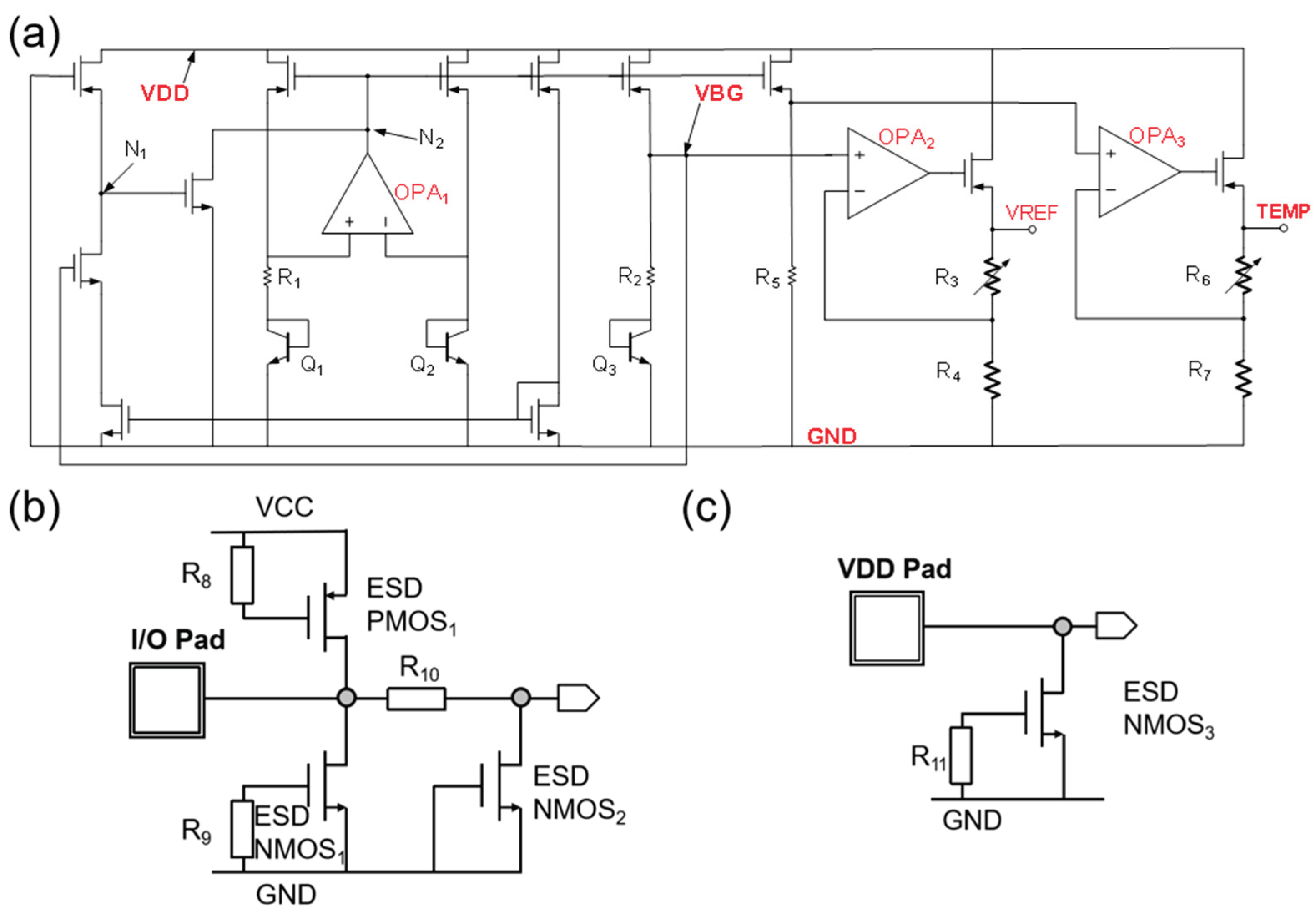
Figure 5.
Fabrication of the flexible hybrid-integrated temperature sensor. (a) Process flow of flexible hybrid integration; (b) Photo of the flexible hybrid-integrated temperature sensor based on the FPC board; (c) Photo of the temperature sensing die mounted on the FPC board; (d) Schematic diagram of the strain distribution in the xx direction when the die mounted on the FPC board is bent with a 10 mm radius.
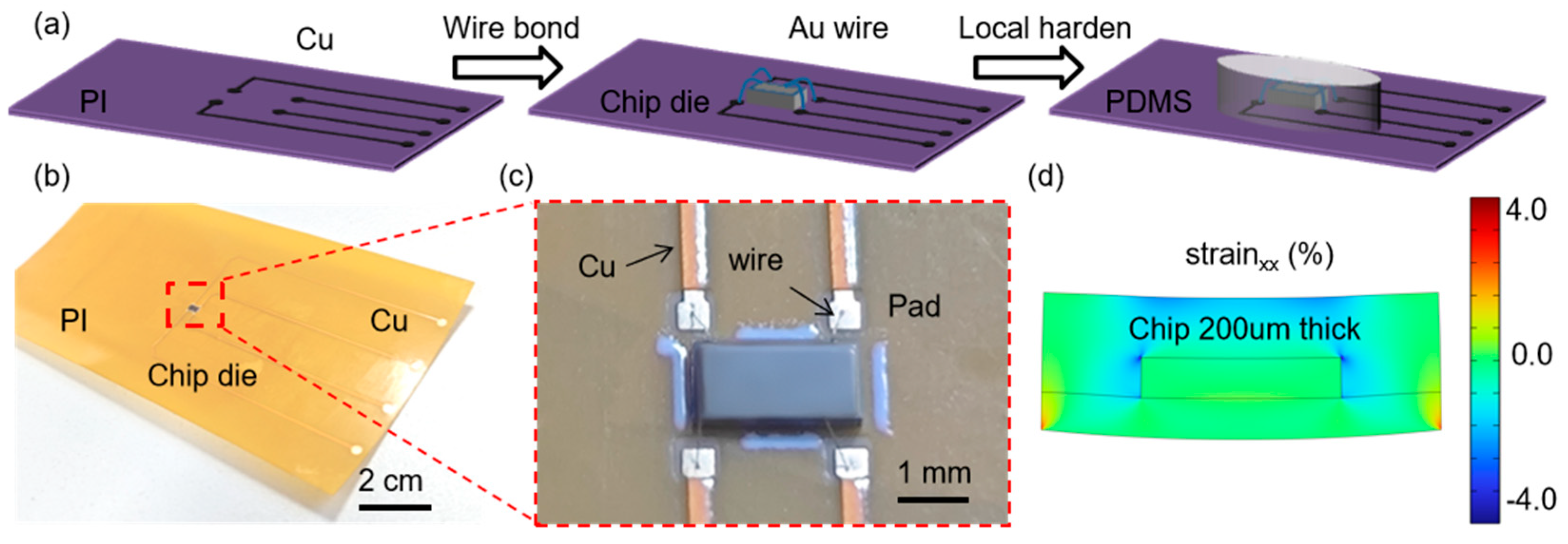
Figure 6.
Testing of the flexible hybrid-integrated temperature sensor. (a) Schematic diagram of the bending test experimental setup; (b) Photograph of the bending test experimental setup; (c) Relationship between the reference voltage output of the flexible hybrid-integrated temperature sensor and the bending radius before bending and after 100 bending cycles; (d) Relationship between the temperature pin voltage output of the flexible hybrid-integrated temperature sensor and the bending radius before bending and after 100 bending cycles; (e) Schematic diagram of the temperature variation test experimental setup; (f) Relationship between the temperature pin voltage output of the flexible hybrid-integrated temperature sensor and the device temperature.
Disclaimer/Publisher’s Note: The statements, opinions and data contained in all publications are solely those of the individual author(s) and contributor(s) and not of MDPI and/or the editor(s). MDPI and/or the editor(s) disclaim responsibility for any injury to people or property resulting from any ideas, methods, instructions or products referred to in the content. |
© 2025 by the authors. Licensee MDPI, Basel, Switzerland. This article is an open access article distributed under the terms and conditions of the Creative Commons Attribution (CC BY) license (http://creativecommons.org/licenses/by/4.0/).
Copyright: This open access article is published under a Creative Commons CC BY 4.0 license, which permit the free download, distribution, and reuse, provided that the author and preprint are cited in any reuse.


