Submitted:
14 August 2025
Posted:
14 August 2025
You are already at the latest version
Abstract
To address the demand for high-density, curved conformal sensing in wearable devices and flexible electronic skin, this paper presents a novel flexible dual-modal sensing array capable of synchronous detection of temperature and magnetic field distributions. We detail the design principles, circuitry, and layout of the core sensing chip. A flexible hybrid integration scheme ensures device flexibility, with single-point tests confirming its excellent dual-modal sensing performance. Mounted on a robotic hand, the array demonstrates simultaneous monitoring of tactile stimuli and environmental temperature. Furthermore, the 6×6 array successfully achieves spatial distribution imaging of both magnetic fields and temperature. This technology holds broad application prospects in human-machine interaction, health monitoring, and robotic tactile perception.
Keywords:
flexible sensing array
; dual-modal sensing
; temperature-magnetic sensing
; tactile perception
; flexible hybrid integration
1. Introduction
Wearable health monitoring, flexible electronic skin, and intelligent robotic sensing systems increasingly demand high-density, multifunctional sensing capabilities that conform seamlessly to complex curved surfaces like the human body [1,2,3,4,5,6]. Such systems require simultaneous monitoring of physiological parameters (temperature distribution) and external stimuli (tactile sensation, magnetic fields) [7,8,9,10]. Directly deposited metal thin films (Pt/Ni sensors) offer accuracy but suffer from immature processes and high costs [11]; carbon-based/organic materials provide flexibility yet struggle to ensure wide-temperature-range linearity, long-term stability for temperature sensing, and sufficient magnetic sensitivity with anti-interference capability [12,13]; while flexible printed circuit board (FPC) hybrid integration of silicon dies balances accuracy and conformability, multi-modal integration introduces inter-die crosstalk, packaging stress effects on multi-parameter accuracy, and high-density array complexity [14,15,16,17].
Silicon-based sensing technologies provide mature solutions: Temperature sensing leverages the negative temperature coefficient of bipolar transistor VBE to generate PTAT voltages via bandgap references [18,19], while Hall effect and magnetoresistance technologies deliver high magnetic sensitivity and stability [20,21]. However, applying these rigid silicon dies in flexible environments introduces packaging stresses that degrade sensing characteristics—manifested as Hall voltage offsets and resistance reference drifts—and obstruct high-density multi-modal array integration [22,23].
To address these challenges, we propose a highly reliable flexible hybrid-integrated dual-modal temperature-magnetic sensing array. Temperature sensing (using optimized bandgap references with low-stress design) and high-sensitivity Hall elements are monolithically integrated on a single die, achieving a temperature coefficient of 5 mV/°C, magnetic sensitivity of ∼96 mV/mT, and magnetic sensitivity drift ≤±2%/°C. Custom multifunctional dies are densely integrated onto ultra-thin FPC via wafer-level microfabrication, minimizing unit size and packaging stress effects on dual-modal performance. A single-point scheme enables tactile-thermal co-measurement, while a 6×6 array (6-mm pitch) achieves spatially resolved simultaneous temperature and magnetic field distribution sensing. This solution combines silicon-grade accuracy with mechanical robustness on a flexible platform, enabling advanced multi-physical field sensing for next-generation wearables, electronic skin, and autonomous robotics.
2. Design and Fabrication
Figure 1 illustrates the core circuit architecture of the monolithically integrated dual-modal sensing die. This architecture comprises two independent functional channels: the temperature sensing channel consists of a bandgap reference source, a PTAT (Proportional to Absolute Temperature) circuit, and an output buffer, delivering a voltage proportional to temperature through the TEMP pin; the magnetic sensing channel includes a bandgap reference source, a Hall plate, an amplifier circuit, and an output buffer, outputting a voltage proportional to magnetic field strength through the HALL pin. The entire die is powered via the VDD and GND pins, enabling synchronous and independent sensing and output of both temperature and magnetic field.
Figure 2 (a) shows the schematic of the temperature sensing circuit, which integrates from left to right a soft-start circuit (to suppress power surges), a bandgap reference core, a PTAT (Proportional To Absolute Temperature) circuit, and a buffer amplifier circuit. The bandgap reference core employs transistors Q1 and Q2 arranged side-by-side with a 16:2 ratio, achieving bias voltage elevation and layout matching. A PTAT voltage division based on the difference in base-emitter voltages of the transistors is generated across resistor R1. The PTAT current is copied by a current mirror into the R2 branch to form a PTAT voltage, which is then proportionally amplified by the buffer amplifier circuit composed of the operational amplifier OPA2 and a resistor feedback network. Finally, a high-drive, high-input-impedance temperature signal is output through the TEMP pin. The temperature sensing output voltage can be expressed by the following equation [24]:
Figure 2 (b) is a schematic of the Hall plate structure, illustrating the three-dimensional structure and cross-section of the magnetic sensing core Hall plate. The device uses an N-type epitaxial layer as the active region, with electrodes brought out via deeply buried N-well connections, and a surrounding P-well process forms isolation rings. The square Hall plate measures 40 μm × 40 μm and produces about 2 mV Hall voltage at its output terminals under a perpendicular magnetic field of 10 mT. This weak signal requires subsequent amplification to meet sensitivity requirements.
Figure 2 (c) presents the schematic of the instrumentation amplifier used to enhance the Hall signal sensitivity. The amplifier features a simple structure, adjustable gain, and low temperature drift. Its voltage gain is determined by the internal resistor network, calculated by the following formula [25,26,27], effectively amplifying the weak Hall voltage signals. In the diagram, pairs of resistors R5 and R6, R7 and R8, and R9 and R10 are symmetrically matched.
Figure 3 (a) presents the chip layout based on the 180nm BCD process, adhering strictly to design rules. The core area includes the bandgap reference source (occupying 0.08 mm², utilizing a common-centroid matching layout to suppress gradient errors), instrumentation amplifier, PTAT circuit, output buffer, and a dual-path ESD protection network (integrated within the VDD/GND pins using large-area clamp transistors, accounting for 22% of the total area), as well as four 80μm × 80μm aluminum-copper alloy pads (VDD, GND, TEMP, HALL).
The periphery is equipped with a double-layer Sealring structure of 20μm width (including a deep contact region grounding ring) to provide mechanical stress buffering. Key signal routing employs shielding protection, with temperature sensing lines at 3μm width and 2μm spacing, and magnetic sensing lines arranged as differential symmetrical pairs with 2μm width and 2μm spacing. The reference voltage paths are symmetrically routed to minimize crosstalk.
Figure 3 (b) shows the layer-removed SEM image of the Hall device, confirming the processing structure matches the design. It exhibits a highly symmetrical 40μm × 40μm square topology with low offset voltage characteristics, suitable for noise reduction techniques such as rotating current and chopping.
Figure 4 (a) illustrates the standardized fabrication process of the flexible hybrid-integrated dual-modal sensor: first, the 1.2 × 0.6 mm² sensor die is precisely mounted on a flexible printed circuit board (FPC) using conductive adhesive. Electrical interconnection is achieved via gold wire bonding, followed by PDMS encapsulation for protection. Subsequently, a transfer platform is used to fix polymer pillars and a magnet assembly (Ø4 mm × 0.5 mm) directly above the sensor die using UV adhesive, completing the magneto-mechanical integration.
Figure 4 (b) shows a photograph of the actual device, validating the structural optimization strategy: the die is thinned to 200 μm by back grinding to reduce bending strain. Finite element analysis indicates that under a bending radius of 20 mm, the maximum lateral strain in the die region is less than 0.6%, and the lateral strain at bonding points is below 3.5% (under the failure threshold), ensuring mechanical robustness under dynamic deformation. The entire process is developed under a fabless model, enabling reproducibility for mass production.
3. Results and Discussion
Figure 5 (a) depicts the mechano-electrical coupling test platform for the flexible dual-modal sensor, integrating a programmable displacement stage (to simulate bending deformation), a high-precision power supply, a digital oscilloscope, and the flexible device under test.
The temperature sensing characteristics shown in Figure 5 (b) demonstrate that the device maintains a linear sensitivity of 5 mV/°C under dynamic bending. The 10 mV peak-to-peak measurement error mainly arises from local stress fluctuations induced by deformation of the flexible substrate, which is within typical application tolerances (<±1.5°C).
Magnetic sensing performance in Figure 5 (c) achieves a system-level sensitivity of 96.6 mV/mT through post-stage multi-level amplification, representing a 483-fold enhancement compared to the original Hall plate sensitivity (0.2 mV/mT). The 15 mV output noise is also modulated by stress, but the signal-to-noise ratio (SNR > 24 dB) meets the requirements of most industrial scenarios.
Figure 5 (d) reveals the device’s stability mechanism under combined stresses: when the bending radius is ≥ 20 mm, the magnetic sensing sensitivity exhibits a temperature drift coefficient of less than ±2% across a wide temperature range of -40 to 125°C. This stability results from three synergistic design features:1) Temperature compensation provided by the bandgap reference; 2) Low temperature drift matching of the instrumentation amplifier’s resistor network; 3) The PDMS encapsulation layer (with a coefficient of thermal expansion ~310 ppm/°C) that buffers thermomechanical stress.
Test results validate that this design possesses strong engineering application potential in dynamic thermo-magnetic coupling environments such as wearable electronics and flexible robotics.
Figure 6 (a) uses finite element simulation to reveal the magnetic basis of tactile sensing: the axial magnetic field strength of a circular magnet (Ø4 mm × 0.5 mm) follows the formula below [28,29,30]:
where is the magnetic induction at the initial reference point, h is the thickness of the magnet disk, R is the radius of the magnet disk, and z is the sensing distance. This model shows that the magnetic field strength decays nonlinearly as distance z increases, as indicated by the white dashed line in the figure.
Figure 6 (b) presents mechanical simulation results illustrating the strain distribution in the polymer support pillar under axial (z-direction) pressure: when pressure is applied, the support pillar elastically deforms, causing the distance z between the magnet and the Hall plate to decrease, which enhances the magnetic field intensity at the Hall sensor. This magneto-mechanical coupling mechanism forms the physical core of tactile perception.
As shown in Figure 6 (c), the sensor is conformally attached to a robotic fingertip via a flexible substrate, achieving imperceptible integration. Dynamic tactile tests in Figure 6 (d) indicate that under light pressure on a hard object, the Hall output voltage increases by approximately 20%, whereas under heavy pressure, it increases by about 60%. This phenomenon originates from the positive correlation between the compression displacement Δz of the magnet gap and the applied pressure, leading to an increase in magnetic field and thus Hall voltage. The rising edge slope of the time-domain signals further differentiates tactile intensity, satisfying high-resolution tactile feedback requirements.
Temperature sensing capability is validated in Figure 6 (e): when the fingertip contacts an ice block (0°C), a 30°C plate, and a 60°C plate, the temperature pin’s output stabilizes at 0.70 V, 0.81 V, and 1.0 V, respectively. Although conformal mounting increases thermal resistance due to PDMS’s low thermal conductivity, the system still achieves an accuracy of ±5°C. Notably, the magneto-thermal dual-modal system exhibits low mutual interference during simultaneous testing, below 1.2%, demonstrating effective decoupling of physical field crosstalk by the architecture design.
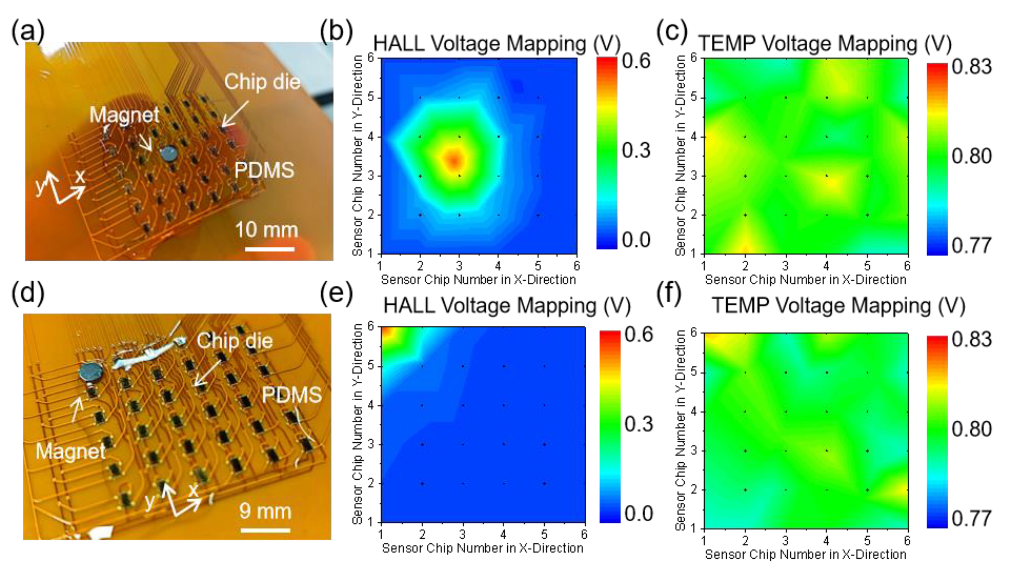
Figure 7 (a, d) show the 36-unit dual-modal flexible array arranged as a 6 × 6 sensor matrix with a 6 mm pitch between units. To accommodate the different dynamic characteristics of magnetic and temperature signals, the Hall sensor outputs are acquired independently and in parallel to capture transient magnetic fields; meanwhile, the temperature signals utilize an innovative time-division multiplexing system. Specifically, the master controller rewrites the phase of each die through the VDD pin, enabling units 1 to 36 to sequentially output temperature voltages and 6-bit verification codes at 1 ms intervals. This allows temperature distribution data transmission over a single data line, significantly improving wiring density compared to traditional parallel schemes.
Figure 7 (b, c) and (e, f) present the spatial response when the magnet is centered and when it is offset to the edge, respectively. When the magnet is centered, the Hall output exhibits a centrally symmetric distribution with a peak voltage of 0.55 V at the array center, achieving a spatial resolution of 6 mm; the temperature distribution shows uniformity within ±0.3°C. After moving the magnet to the edge, the Hall output accurately tracks the position change with an edge response of 0.50 V, and the temperature distribution remains uniformly controlled within ±0.3°C. The array maintains good magnetic positioning accuracy and temperature sensing precision even under bending radii greater than 20 mm, providing essential technical support for electronic skin applications.
4. Conclusions
In summary, this work realizes a high-density flexible hybrid-integrated dual-modal temperature–magnetic sensing array, overcoming multimodal fusion bottlenecks through a single-die collaborative sensing architecture. On a 1.2 × 0.6 mm² die, temperature sensing channel (bandgap reference optimized design with 5 mV/°C sensitivity) and magnetic sensing module (Hall element with 96 mV/mT sensitivity and temperature drift ≤ ±2%) are integrated. Combined with wafer-level micromachining and ultra-thin FPC mounting techniques, packaging-induced stress effects are significantly suppressed. The single-point tactile–temperature synergistic measurement mechanism is demonstrated, and a 6 × 6 magnetic–temperature sensing array with 6 mm unit pitch is constructed to achieve spatially resolved dual-physical-field synchronous perception. This approach strikes a balance between silicon-based precision and flexible robustness, offering a novel multi-physical-field sensing paradigm for smart wearable devices, bionic electronic skin, and autonomous robotics.
Funding
This work was supported by the National Key Research and Development Program of China (2022YFB3207703) and the Key Research and Development Program of Ningbo (2023Z153).
Institutional Review Board Statement
Not applicable.
Informed Consent Statement
Not applicable.
Data Availability Statement
The data presented in this study are available upon request.
Acknowledgments
The authors thank Ningbo CRRC Times Transducer Technology Co., Ltd. , the College of Electrical Engineering at Zhejiang University and School of Electrical Engineering at Southeast University for facility support.
Conflicts of Interest
The authors declare no conflicts of interest.
References
- Deng, Z.Y.; Guo, L.H.; Chen, X.M. Smart wearable systems for health monitoring. Sens. 2023, 23, 2479. [Google Scholar] [CrossRef]
- Yang, H.; Li, S.; Wu, Y. Advances in flexible magnetosensitive materials and devices for wearable electronics. Adv. Mater. 2024, 36, 202311996. [Google Scholar] [CrossRef]
- Yoon, H.; Park, S.H. A nontouchscreen tactile wearable interface as an alternative to touchscreen-based wearable devices. Sens. 2020, 20, 1275. [Google Scholar] [CrossRef]
- Hegde, C.; Su, J.T.; Tan, J.M.R. Sensing in soft robotics. ACS Nano. 2023, 17, 15277–15307. [Google Scholar] [CrossRef]
- Liu, S.Z.; Guo, W.T.; Chen, H. Recent progress on flexible self-powered tactile sensing platforms for health monitoring and robotics. Small. 2024, 20, 240. [Google Scholar] [CrossRef]
- Luo, Y.; Sun, C.L.; Wei, M.L. Integrated flexible microscale mechanical sensors based on cascaded free spectral range-free cavities. Nano Lett. 2023, 23, 8898–8906. [Google Scholar] [CrossRef] [PubMed]
- Dou, W.Q.; Zhong, G.L.; Cao, J.L. Soft robotic manipulators: designs, actuation, stiffness tuning, and sensing. Adv. Mater. Technol. 2021, 6, 2100018. [Google Scholar] [CrossRef]
- Ma, Z.; Ding, C.; Li, L. The design of decoupled robotic arm based on chain transmission. Mach. 2024, 12, 410. [Google Scholar] [CrossRef]
- Wang, Y.; Wu, W.; Li, S. A soft mimic robotic arm powered by dielectric elastomer actuator. Adv. Funct. Mater. 2024, 34(52).
- Chen, L.; Zhao, Y.; Shen, Y. 3D stitching double weave fabric-based elastic triboelectric nanogenerator for energy harvesting and self-powered sensing. energies. 2023, 16, 2284. [Google Scholar] [CrossRef]
- Jang, H.; Park, Y.J.; Chen, X. Graphene based flexible and stretchable electronics. Adv. Mater. 2016, 28, 4184–4202. [Google Scholar] [CrossRef] [PubMed]
- Donolato, M.; Tollan, C.; Porro, J.M. Flexible and stretchable polymers with embedded magnetic nanostructures. Adv. Mater. 2013, 25, 623–629. [Google Scholar] [CrossRef]
- Heng, W.Z.; Solomon, S.; Gao, W. Flexible electronics and devices as human-machine interfaces for medical robotics. Adv. Mater. 2022, 34, 2107902. [Google Scholar] [CrossRef] [PubMed]
- Luo, Y.; Fang, Y.; Lv, Y. Flexible hybrid integration hall angle sensor compatible with the CMOS process. Sens. 2025, 25, 927. [Google Scholar] [CrossRef] [PubMed]
- Ma, Y.; Zhang, Y.; Cai, S. Flexible hybrid electronics for digital healthcare. Adv. Mater. 2020, 32, 1902062. [Google Scholar] [CrossRef]
- Neto, M.; Ribeiro, P.; Nunes, R. A soft tactile sensor based on magnetics and hybrid flexible-rigid electronics. Sens. 2021, 21, 5098. [Google Scholar] [CrossRef] [PubMed]
- Borghetti, M.; Cantù, E.; Sardini, E. Future sensors for smart objects by printing technologies in industry 4. 0 scenario. energies. 2020, 13, 5916. [Google Scholar] [CrossRef]
- Chang, J.; Yin, Y.L.; Du, J.H. On-chip integrated high-sensitivity temperature sensor based on p-GaN/AlGaN/GaN heterostructure. IEEE Electron Device Lett. 2023, 44, 594–597. [Google Scholar] [CrossRef]
- Hedayati, R.; Lanni, L.; Rusu, A. Wide temperature range integrated bandgap voltage references in 4H-SiC. IEEE Electron Device Lett. 2016, 37, 146–149. [Google Scholar] [CrossRef]
- Kaidarova, B.A.; Liu, W.H.; Swanepoel, L. Flexible Hall sensor made of laser-scribed graphene. npj Flexible Electron. 2021, 5, 2. [Google Scholar] [CrossRef]
- Mirfakhraei, S.S.; Audet, Y.; Hassan, A. A small footprint digital isolator based on CMOS integrated hall effect sensor. IEEE Sens. J. 2022, 22, 412–418. [Google Scholar] [CrossRef]
- Shih, W.P.; Tsao, L.C.; Lee, C.W. Flexible temperature sensor array based on a graphite-polydimethylsiloxane composite. Sens. 2010, 10, 3597–3610. [Google Scholar] [CrossRef] [PubMed]
- Arora, E.K.; Sharma, V.; Ravi, A. Polyaniline-based ink for inkjet printing for supercapacitors, sensors, and electrochromic devices. energies. 2023, 16, 6716. [Google Scholar] [CrossRef]
- Wang, Z.; You, H.; Yang, D.W. High-performance flexible thermoelectric sensor for temperature perception. ACS Appl. Electron. Mater. 2025, 7, 1283–1290. [Google Scholar] [CrossRef]
- Hamid, S.S.; Mariappan, S.; Rajendran, J. A state of the art review on CMOS radio frequency power amplifiers for wireless communication systems. Micromachines. 2023, 14, 1551. [Google Scholar] [CrossRef]
- Kusuda, Y. A 5. 6 nV/√Hz chopper operational amplifier achieving a 0.5 μV maximum offset over rail to rail input range with adaptive clock boosting technique. IEEE J. Solid-State Circuits. 2016, 51, 2119–2128. [Google Scholar]
- Mirfakhraei, S.S.; Audet, Y.; Hassan, A. A galvanic isolated amplifier based on CMOS integrated hall effect sensors. IEEE Trans. Circuits Syst. I Regul. Pap. 2021, 68, 1388–1397. [Google Scholar] [CrossRef]
- Jouyaeian, A.; Fan, Q.; Ausserlechner, U. A hybrid magnetic current sensor with a dual differential DC servo loop. IEEE J. Solid-State Circuits. 2023, 58, 3442–3449. [Google Scholar] [CrossRef]
- Karnaushenko, D.; Makarov, D.; Stöber, M. High performance magnetic sensorics for printable and flexible electronics. Adv. Mater. 2015, 27, 880–885. [Google Scholar] [CrossRef]
- Pan, L.L.; Xie, Y.L.; Yang, H.L. Flexible magnetic sensors. Sens. 2023, 23, 4083. [Google Scholar] [CrossRef]
Figure 1.
Circuit architecture diagram of the dual-modal temperature-magnetic sensing die.
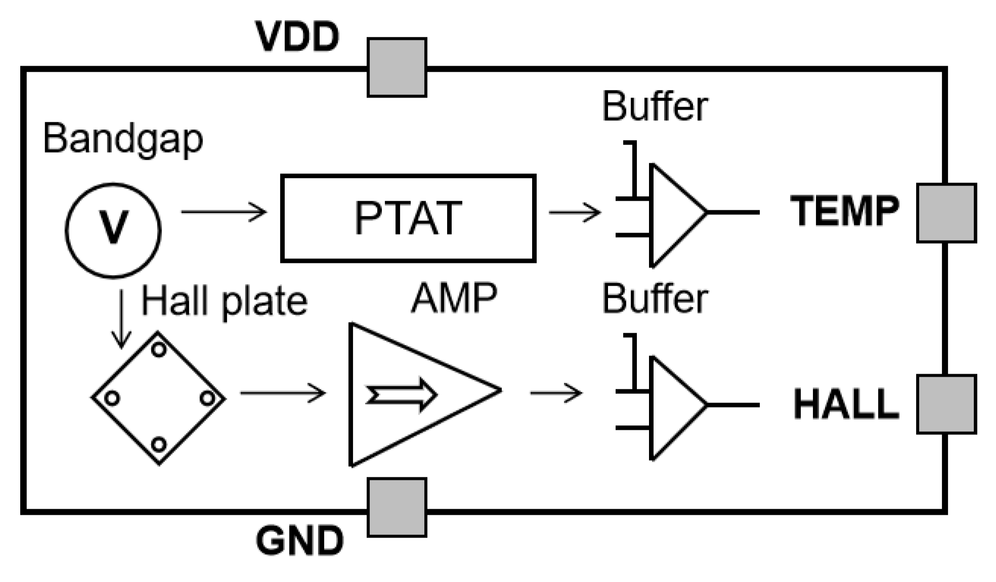
Figure 2.
Circuit schematic. (a) Circuit schematic of the temperature sensing signal generation; (b) Schematic diagram of the Hall plate; (c) Circuit schematic of the Hall signal amplification.
Figure 2.
Circuit schematic. (a) Circuit schematic of the temperature sensing signal generation; (b) Schematic diagram of the Hall plate; (c) Circuit schematic of the Hall signal amplification.
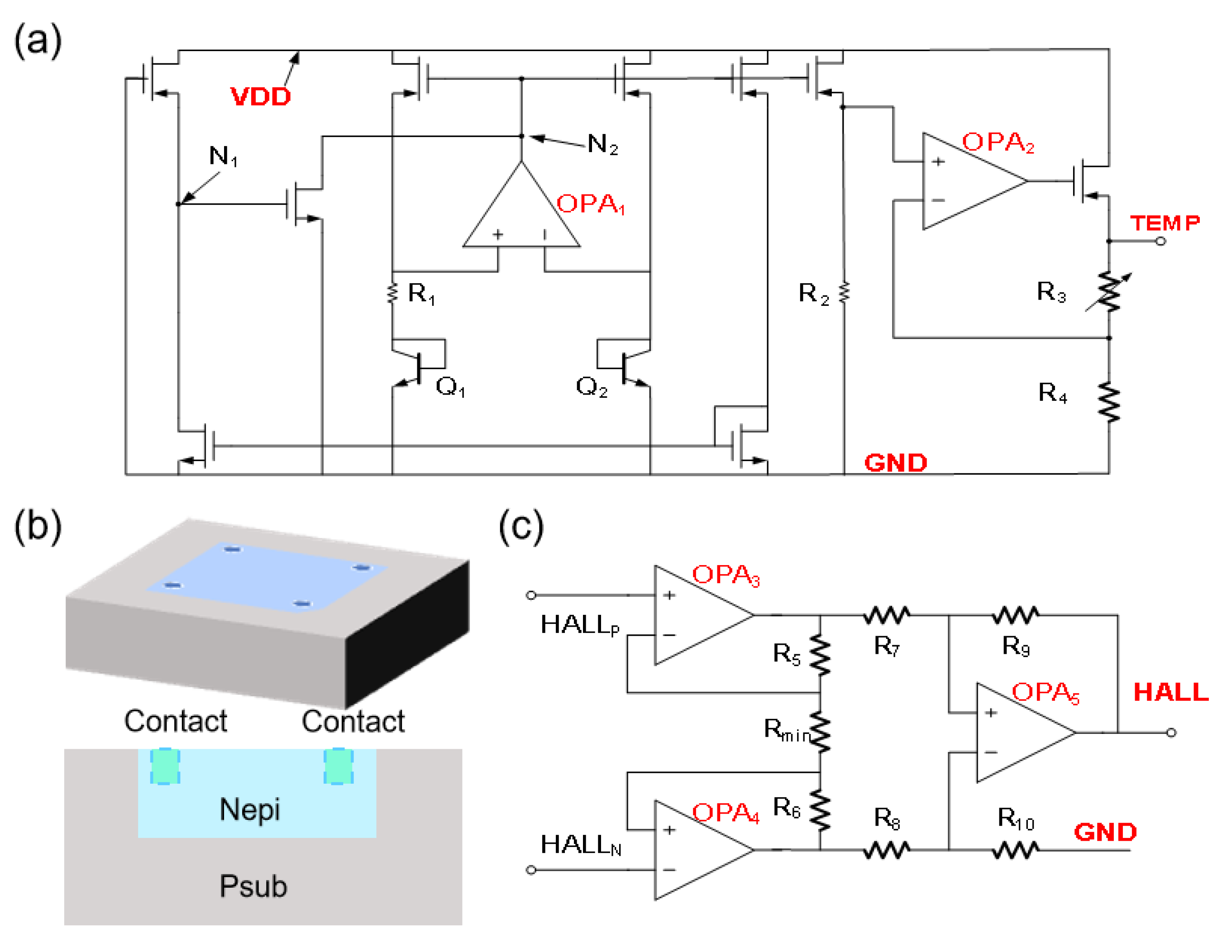
Figure 3.
(a) Layout based on the foundry's PDK; (b) SEM image of the Hall plate after layer removal.
Figure 3.
(a) Layout based on the foundry's PDK; (b) SEM image of the Hall plate after layer removal.
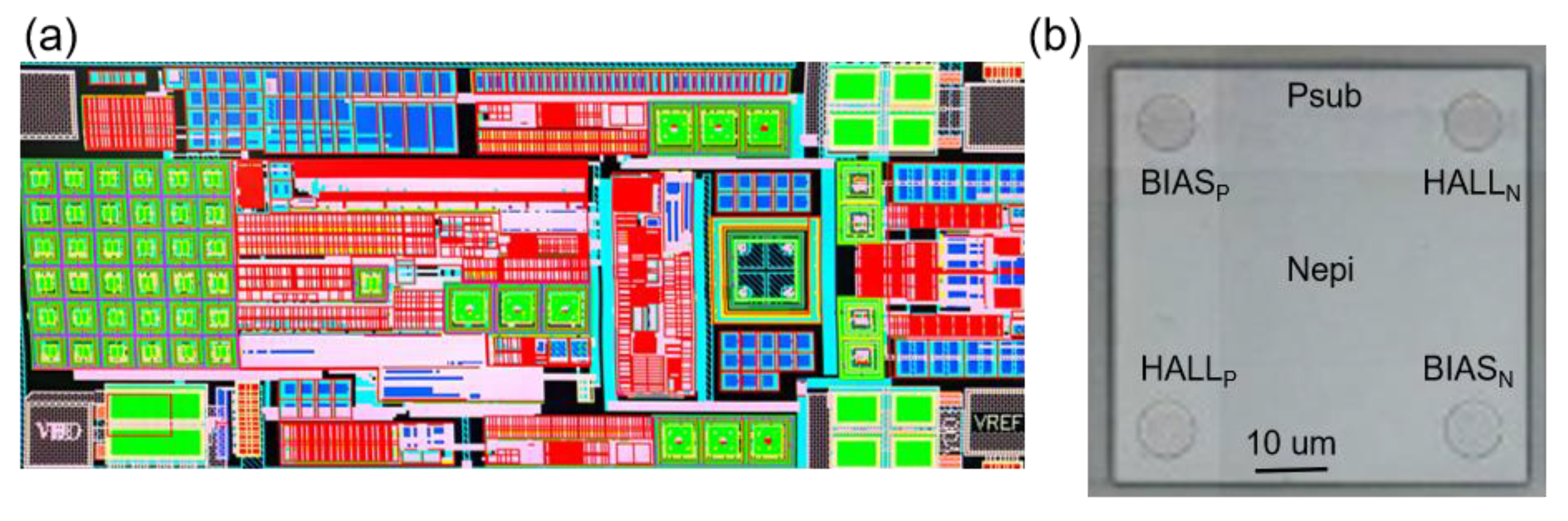
Figure 4.
Fabrication of the flexible hybrid-integrated dual-modal sensor. (a) Process flow of flexible hybrid integration; (b) Photograph of the flexible hybrid-integrated dual-modal single-point sensor based on the FPC board; (c) Schematic diagram of strain distribution in the xx direction when the die mounted on the FPC board is bent with a 20 mm radius.
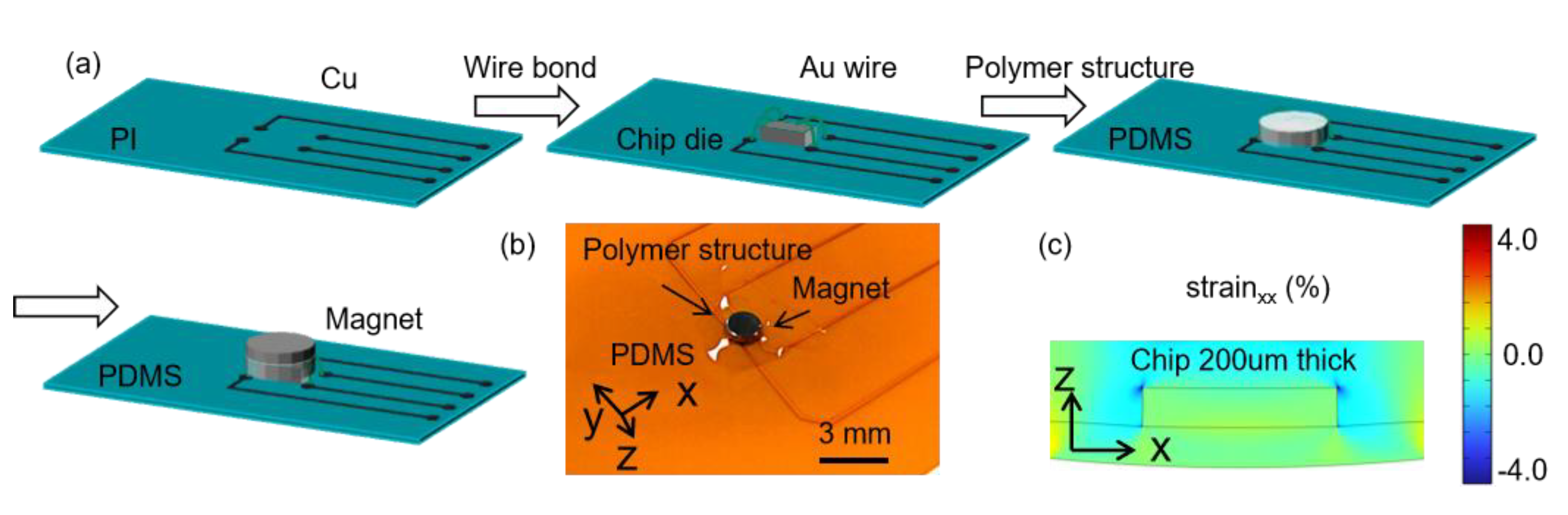
Figure 5.
Testing of the flexible hybrid-integrated dual-modal sensor. (a) Schematic diagram of the bending test experimental setup; (b) Flexible hybrid-integrated temperature sensing; (c) Relationship between magnetic field and the magnetic pin voltage output of the flexible hybrid-integrated temperature sensor; (d) Relationship between magnetic sensing sensitivity shift and device temperature of the flexible hybrid-integrated temperature sensor.
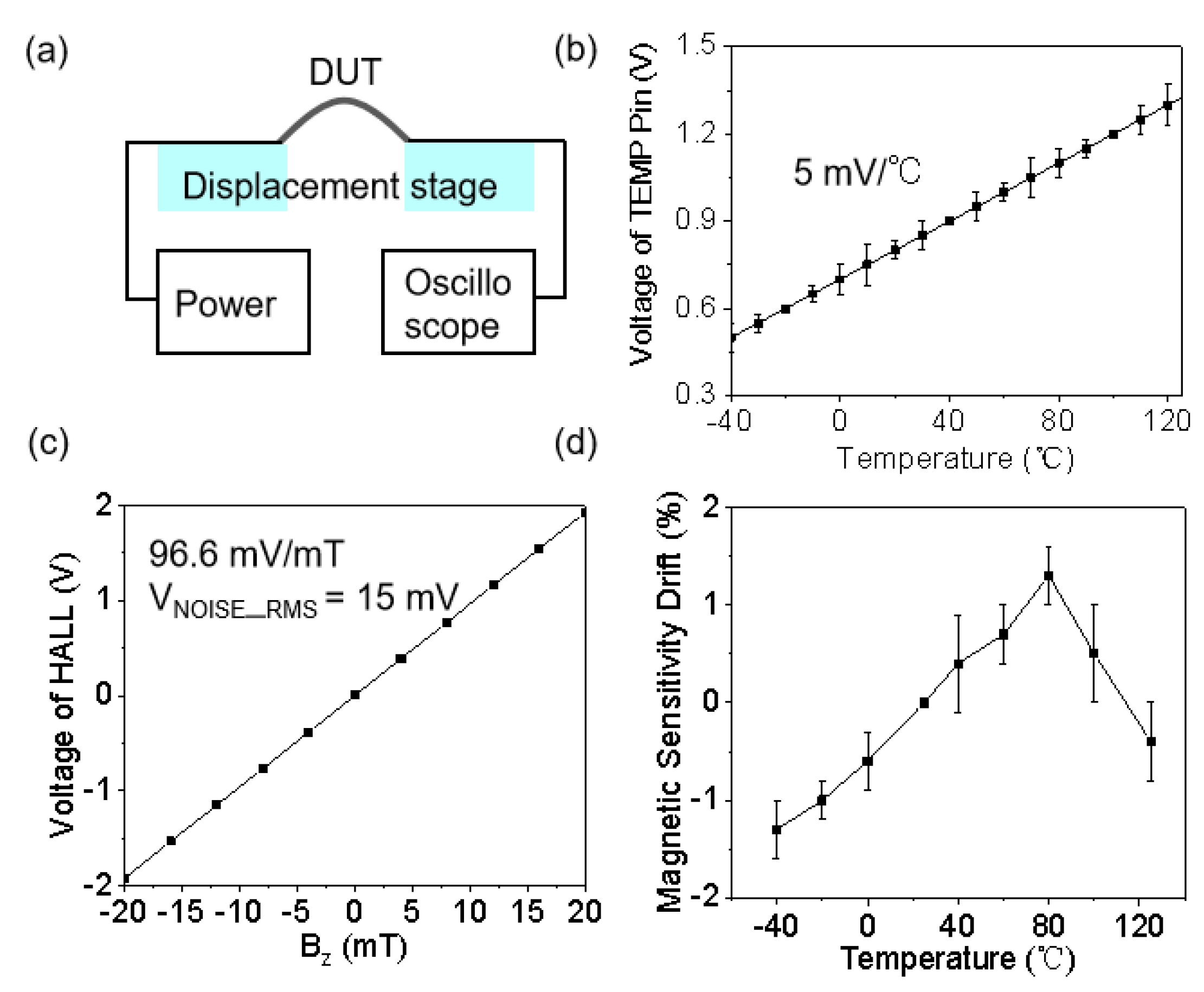
Figure 6.
Tactile sensing application of the flexible hybrid-integrated dual-modal sensor. (a) Magnetic field distribution simulation of the surface magnet; (b) Principal strain distribution simulation of the polymer structure serving as the support layer under z-direction stress; (c) Photo of the flexible tactile sensor attached to the fingertip surface; (d) Time-domain signals of the Hall pin output voltage measured when the fingertip applies heavy and light pressure on a hard object; (e) Temperature pin output voltage signals when the fingertip touches ice, a 30°C hot plate, and a 60°C hot plate.
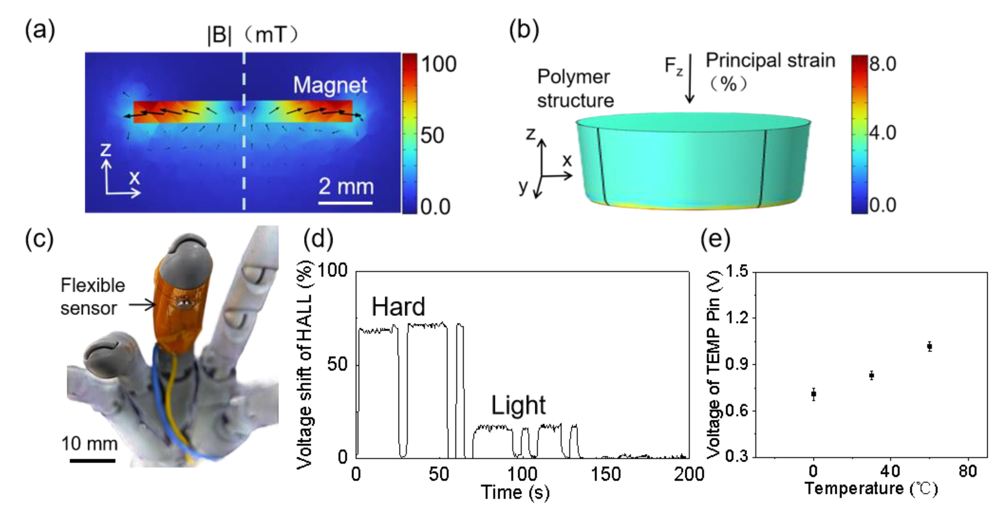
Figure 7.
Testing of the high-density flexible hybrid-integrated dual-modal sensing array. (a) Photograph of the high-density flexible hybrid-integrated dual-modal sensing array positioned at the center of a magnet; (b) Distribution of the Hall pin output voltage; (c) Distribution of the temperature pin output voltage; (d) Photograph of the high-density flexible hybrid-integrated dual-modal sensing array positioned at the edge of a magnet; (e) Distribution of the Hall pin output voltage; (f) Distribution of the temperature pin output voltage.
Disclaimer/Publisher’s Note: The statements, opinions and data contained in all publications are solely those of the individual author(s) and contributor(s) and not of MDPI and/or the editor(s). MDPI and/or the editor(s) disclaim responsibility for any injury to people or property resulting from any ideas, methods, instructions or products referred to in the content. |
© 2025 by the authors. Licensee MDPI, Basel, Switzerland. This article is an open access article distributed under the terms and conditions of the Creative Commons Attribution (CC BY) license (http://creativecommons.org/licenses/by/4.0/).
Copyright: This open access article is published under a Creative Commons CC BY 4.0 license, which permit the free download, distribution, and reuse, provided that the author and preprint are cited in any reuse.


