
Submitted:
28 July 2025
Posted:
29 July 2025
You are already at the latest version
Abstract
We demonstrate that selective electrochemical etching is a reliable method for detecting and observing the uneven concentration distribution of impurities in indium phosphide crystals, which accompanies the growth of highly doped crystals using the Czochralski method. Even though selective electrochemical etching, as a method of detecting defects in the crystal lattice, has been discussed many times in the literature, it has not yet been described for indium phosphide. In this work, we investigated etching in compositions of various selective electrolytes for InP of n- and p-type conductivity with different surface orientations. We present in detail the features of detecting the striped inhomogeneity of impurity distribution. The mechanisms and peculiarities of the formation of oxide crystallites on the surface of InP during electrochemical processing are presented, including structures like flower-like and parquet crystallites. The formation of porous surfaces, terraces, tracks, and crystallites is explained from the perspective of the defect-dislocation mechanism.
Keywords:
segregation stripes
; impurity
; growth bands
; crystallites
; surface
; dislocations
; electrochemical etching
; selective etchant
1. Introduction
The development of modern microelectronics requires researchers to create new materials with improved characteristics. At the same time, such materials must be characterized by reliability and stability of properties. Significant progress has been achieved using doping impurities in the growth of semiconductor crystals [1,2]. In particular, doping technologies have improved the characteristics of LEDs and solar cells [3,4]. Doping is crucial for tuning carrier injection properties at the metal/semiconductor interface [5].
An essential aspect of introducing doping impurities is the growth of crystals with controlled and regulated characteristics. The type of impurity and its content determines the type of conductivity, specific resistance, carrier concentration, mobility, etc. [6,7].
Among modern semiconductor materials, indium phosphide (InP) occupies a special place thanks to a range of unique properties [8,9]. Indium phosphide is used in photonic integrated circuits, laser technology, and photonics [10,11,12]. The radiation resistance of indium phosphide makes it a promising material for photovoltaics, particularly in space solar cells [13,14]. It has also been reported that InP is used as a substrate for growing epitaxial layers of nitrides [15,16].
The primary method for growing monocrystalline indium phosphide is the Czochralski process [17]. In this process, engineers face the challenge of controlling defects, as monocrystals with a high doping level tend to form many defects, including dislocation loops and clusters, point defects, and surface-related defects [18,19]. Moreover, dislocations serve as centers for powerful recombination carriers [20]. This can lead to severe degradation effects in devices [21]. Despite the extensive research on the impact of doping on the electrophysical and optical properties of semiconductors with various impurities, little work has been dedicated to the distribution of impurities in the volume of the crystal, i.e., the internal macromorphology of crystalline semiconductors.
Since direct observation of semiconductor defects is quite challenging, selective chemical or electrochemical etching is the most common and appropriate method for their observation [22,23]. Under certain conditions and with specific electrolytes, etch pits are observed on the crystal surface at the sites of defect concentration, which can be used to assess the nature and concentration (density) of semiconductor defects [24,25].
In this work, we summarize the results of many years of research on the morphology of indium phosphide and the influence of segregation phenomena on the processes of electrochemical dissolution of InP. Our choice is motivated by observing segregation phenomena through etch pits in semiconductors with different conductivity types and surface orientations. We demonstrate that Scanning Electron Spectroscopy (SEM) is an effective tool for studying the surface morphology of nanostructured semiconductor layers and can also be efficiently applied in assessing the distribution of impurities and defects within the crystal volume.
2. Materials and Methods
For the experiment, we used sets of single crystalline indium phosphide of n- and p-type, doped to a carrier concentration of 2.3x1018 cm-3. The plates were cut from identical ingots with dimensions of 2x10x20 mm (Table 1).
Before the experiment, the plates were mechanically (with diamond paste) and chemically (with a polishing etchant) polished. After this, the plates were washed in distilled water and degreased in an alcohol solution. The method of electrochemical etching in solutions of selective etchants was chosen to study the correlations between segregation phenomena and changes in the morphological indicators of indium phosphide.
Aqueous and aqueous-alcohol hydrofluoric, nitric, and hydrochloric acid solutions were used as selective etchants. During the experiment, changes in the anodizing current were recorded. Fluctuations in the current determined the stages of electrochemical dissolution of the samples, and accordingly, the etching time was adjusted.
The investigation of etching figures was conducted using a JEOL-6490 scanning electron microscope.
3. Results
3.1. Investigation of Etch Pits on the Surface of InP with Different Crystallographic Orientations
Figure 1 demonstrates the surface morphology of indium phosphide samples of different crystallographic orientations during electrochemical etching in hydrochloric, hydrofluoric, and nitric acid solutions using a 25% solution by weight of each etchant. The samples were etched at a constant voltage of U=3V. It can be seen that in different acids, InP crystals are etched with the formation of a unique microrelief. However, general trends can be identified.
Samples n-InP with a (100) surface orientation are etched with the formation of tiny pores evenly distributed over the surface (Figure 1a–c). Such pores are oriented along the current and grow deep into the crystal in thin, mutually parallel channels. Depending on the composition of the electrolyte, the diameter of such pores varies from 20 nm to 100 nm, and the porosity can reach 80%. The pores are cylindrical, oriented along the direction of the electric current, and extend deep into the crystal lattice, forming thin parallel channels. The porosity level can reach 80%, indicating a significant alteration in the crystal structure. The size and distribution of the pores change depending on the type of electrolyte used. In hydrochloric acid, the pores are more uniform and diminutive, whereas in hydrofluoric acid, they tend to be larger and more dispersed. A moderate pore size with a more rugged surface texture is observed in nitric acid.
N-InP samples with a (111) surface orientation demonstrate the formation of massive etch pits, tracks, and steps, indicating a more aggressive dissolution process (Figure 1d,e). Electrochemical treatment often results in the formation of oxide crystallites on the surface, especially noticeable in samples etched with hydrofluoric acid (Figure 1f). The most active electrochemical dissolution processes were manifested precisely during the etching of n-InP with a (111) surface orientation. The surfaces oriented towards (111) exhibit the most dynamic etching patterns with deep, irregular pits and pronounced crystalline features.
On the other hand, n-InP with a (001) orientation shows diverse morphological changes depending on the etching solution. In hydrochloric acid, cracks with embedded crystallites appear on the surface (Figure 1g). In hydrofluoric acid, extensive etching pits are formed (Figure 1h), while in nitric acid, relatively smaller pores are observed (Figure 1i).
InP samples of p-type conductivity demonstrate less susceptibility to electrochemical processing than n-type InP (Figure 1j,k). These samples show textured surfaces with either dispersed textures or isolated small etching pits. This suggests a more restrained etching process, likely due to the different electrical properties of p-type InP.
Overall, the study emphasizes the significant influence of crystallographic orientation on the etching behavior of InP. The (111) orientation is particularly prone to pronounced etching effects, making it suitable for studying surface and volume defects through selective electrochemical etching. These findings have implications for the fabrication of semiconductor devices, where control over surface morphology at the nanoscale can impact device performance.
3.2. Formation of Growth Defects in InP during Czochralski Method Growth
A layered heterogeneity in the distribution of defects is observed during the growth of indium phosphide using the Czochralski method [26]. As demonstrated in Figure 1e,f, this manifests as concentric rings during the etching of n-InP (111) in selective etchants. These rings result from uneven distribution of impurities within the semiconductor volume during crystallization.
To understand the processes of uneven impurity distribution in grown single crystal ingots, let us briefly present the key points. The crucible has a melt-in contact with a seed crystal. The seed crystal is slowly released, allowing atoms from the melt to attach. An important aspect is that the seed crystal has a slightly lower temperature than the melt. As a result of this process, temperature gradients arise that affect the growth boundary.
Excessive concentrations of impurities in some crystal regions can lead to the formation of their complexes, which can be considered a new system component. Thus, uneven crystallization is observed during the growth of highly doped semiconductors using the Czochralski method, which is facilitated by new degrees of freedom. In other words, it can be asserted that phase transformations occurring at the boundary of areas with different impurity concentrations lead to the appearance of coherent and incoherent boundaries. Coherent boundaries do not disturb the structure and monocrystallinity of the semiconductor ingot. Incoherent boundaries, due to significant interphase differences, lead to the breaking of bonds and the formation of an intercrystalline border. This is manifested as the striation of the crystal structure.
Doping semiconductors with donor impurities to high concentrations leads to the appearance of micro defects and dislocations. Moreover, impurity atoms cause intrinsic point defects, among which are substitution atoms, interstitial atoms, vacancies, Frenkel pairs, and others. The presence of a high concentration of point defects, in turn, leads to twinning and dislocation clusters. This is manifested in segregation phenomena. In this sense, the impurity concentration can be considered a function of crystal growth.
Segregation lines exhibit periodicity and are striated. The cyclicality of the crystal growth rate can explain striation. The growth rate's nonlinear character is due to dislocations in the crystal volume and the uneven distribution of the doping impurity.
Segregation lines appear as continuous lines perpendicular to the growth direction of the semiconductor grown from the melt (Figure 2). The accumulation of doping impurities, caused by fluctuations in the microscopic growth rate, occurs due to an imbalance in convection through temperature fluctuations at the seed/melt interface [27]. In Figure 2, one can observe etching figures on the surface of n-InP (111), which result from a selective etchant (HF solution) on areas of excess impurity content and impurity-depleted zones. Growth bands, which appear as areas with a high density of etch pits, are separated by unetched areas (Figure 2(1)).
Segregation lines show an exciting feature. One edge has a clear boundary dividing the zones of excess and depleted impurity content (Figure 2(2)). Then, there is a gradual decrease in the number of etch pits (Figure 2(3)). Areas (4) in Figure 2 show the edge of the segregation band, which is "blurred." In these areas, the concentration of pores (etch pits) is significantly lower due to the lower impurity concentration. Such observations indicate the direction of crystal growth. The width of the zone with increased impurity concentration is 100 nm, and the depleted zone is 120 µm. Our work investigates the concentration inhomogeneity of impurity distribution in more detail [28].
Consequently, we observe an increase in the concentration of inlet pores from the center to the periphery of the sample, which also gives an idea of the direction of crystal growth (in Figure 1, the direction of crystal growth is indicated by arrows). It should be noted that growth bands can affect the crystal lattice parameters within the zone of excessive impurity content but almost do not affect the change in lattice constants between bands [29,30]. Also, growth bands may appear due to the emergence of so-called "dislocation walls," which manifest as irregular lines running perpendicular to the growth front. Dislocation walls arise due to the inhomogeneous accumulation of doping impurities along the growth front, transitioning from one layer to another as the crystal grows [31,32].
Such a sectoral distribution into zones of excessive impurity content and, conversely, impurity-depleted zones can, in turn, lead to the appearance of screw dislocations [33,34]. The semiconductor crystal around a screw dislocation represents a single atomic plane. Spiral steps move around the dislocation as excess impurity atoms are adsorbed on the surface. As a result, crystal growth is observed without the nucleation of new layers, i.e., the formation of a growth spiral (Figure 3). It can be seen that the height of the step is 5 µm. As a result of electrochemical etching, the steps delaminate into bands 1 µm wide. Their surface becomes loose and porous.
Generally, the screw dislocation plays a crucial role in crystal growth from the melt [35]. As mentioned earlier, such a dislocation represents a single atomic plane that grows around the dislocation axis due to the addition of atoms to an infinite source of kinks [36,37]. In turn, the step is anchored at the point of dislocation emergence [38]. The step’s inner parts rotate faster than the outer ones [39], causing the step to twist into a spiral.
During the cooling of the forming ingot from the melt, homogeneity of composition is determined by convective processes. Horizontal temperature and impurity concentration gradients cause significant axial and radial inhomogeneity. Moreover, the distribution of impurities in the crystal can be inhomogeneous not only along but also across the axis of crystal growth, as demonstrated in Figure 4. In this case, changes in the lattice parameter of the solid solution can cause elastic stresses [40,41].
Thus, temperature fluctuations in the crystallization zone significantly impact the formation of growth bands. These temperature fluctuations arise due to two mechanisms. Firstly, the crystal growth rate may vary across the crucible due to asymmetry in the temperature field. Secondly, convective processes can also cause temperature fluctuations.
3.3. Investigation of Etch Pits Along Dislocation Slip Lines
When etching the crystal in selective etchants, the formation of etch pits along slip lines and dissolution channels, which form close to the etch pits, can be observed (Figure 5). The diameter of etch pits caused by this phenomenon is 100 nm. The length of the dissolution channel can reach up to 10 µm. In Figure 5c, the formation of tracks between pores with lengths ranging from 1 to 3 µm can be seen. The tracks’ cross-section thickness is between 100 to 200 nm. The aspect ratio ranges from 20 to 50.
Etch pits can form both on edge and screw dislocations. A dislocation is a source of elastic mechanical stresses, causing the formation of elastic deformations around it. Therefore, during the etching of InP in selective etchants, dislocations serve as the nucleation sites for forming primary (germinal) pores. Moreover, a dislocation can interact with point defects in the crystal volume, leading to an increased concentration of residual defects near the dislocation axis (the so-called "Cottrell atmosphere") [42,43,44].
An interesting observation is that dissolution channels and tracks always intersect at an angle of 135°С. After the intersection, they do not change their direction (Figure 6). This phenomenon is due to the anisotropy of InP and is manifested exclusively in the etching of (111) oriented samples.
3.4. Formation of Oxide Crystallites at Sites of Accumulation of Defects in the Crystal Lattice
Alternative electrochemical reactions can also accompany the process of electrochemical etching. These primarily include electrochemical polishing of the surface due to the etching of all surface irregularities. Furthermore, during etching, the surface can become covered with a continuous inseparable film, resulting from chemical interactions of the surface layers of indium phosphide with electrolyte ions. These films are typically oxide compounds of the first or second element of the semiconductor [45]. Such oxides can inhibit further dissolution of the crystal. In such a case, the etching process stops. Often, a continuous film, due to lattice mismatch with the substrate material (the semiconductor itself), can crack and split. This leads to the crystal's re-etching at the film rupture sites. The formation of a porous space on the film itself can also occur. As a result of such behavior, the film becomes loose and is easily removed from the substrate.
The most important observation in this process is that the rupture of the film does not occur at spontaneous locations but specifically in areas of excessive impurity concentration. This is because such areas are supersaturated with dislocations. As a result, the formation of orderly "parquet" type oxide crystallites can be observed on the crystal surface (Figure 7).
The geometric dimensions of the crystallites are almost equal: length (100 – 130) µm, width and height about 7 µm. The distance between neighboring crystallites is 2 µm, between parquet blocks – (30 – 50 µm). The crystallites have a porous structure. It can be seen that the parquet blocks and crystallites easily align with each other. This indicates that the crystallites formed due to the spreading of the oxide film due to the action of elastic stresses [46]. The longitudinal uniform shift of adjacent steps relative to each other occurs due to the slippage of dislocation loops. The shift stops after the partial emergence of the loop on the surface. Also, the exits of dislocation loops are observed in areas of excessive impurity concentration, i.e., along segregation lines.
Often on the surface of n-InP (111) during electrochemical processing, in areas of excessive impurity concentration, oxide crystallites of the flower type are formed (Figure 8a–c). The mechanism of this phenomenon is as follows. The rate of electrochemical deposition of reaction products on the surface (i.e., the growth of crystallites) depends on the arrival of atoms to the surface, as well as on the structure of the surface and processes occurring at the electrolyte/semiconductor interface.
Figure 8e presents a cross-section and boundary of the semiconductor/electrolyte with a flat (ideal) surface. Each surface atom of such a crystal has bonds with atoms in the volume. Thus, the surface energy is low, and the formation of new nucleation centers for crystallites is complicated due to the small number of broken bonds.
Dislocations that emerge on the crystal's surface due to electrochemical etching are active centers of chemical reactions. Figure 8f shows that the surface atoms, due to the formation of pores, do not have all their "neighbors»; thus, the surface is characterized by many broken bonds. This means that atomically rough and imperfect surfaces have a higher rate of electrochemical deposition, i.e., a higher growth rate of oxide crystallites.
Also, the inhomogeneous distribution of impurities and their excessive concentration in segregation bands causes the appearance of a network of grain boundaries. Grain boundaries consist of individual dislocations or agglomerations of dislocations, forming so-called "dislocation walls." Grain and subgrain boundaries are formed in ingots due to thermal stress during crystal growth. Grain boundaries act as charge capture centers, causing spatial inhomogeneity in charge transport, thereby impairing charge transfer. These walls and grain boundaries are nucleation centers for oxide crystallites on the crystal surface.
Thus, the study of defects in single crystals caused by impurity atoms is an essential factor in controlling the transport characteristics of electronic and photonic devices. The ability to manage defects by reducing or increasing their quantity could be the next step in creating modern functional materials. Eliminating impurity defects and concentration inhomogeneity in highly doped semiconductors is quite challenging. This necessitates further research to improve material quality by optimizing growth parameters and managing impurity defects. Efforts may be directed towards finding optimal conditions for thermal annealing of the semiconductor ingot, which can significantly reduce strained states in the semiconductor by creating new types of defects (stamping defects).
4. Discussion
Authors should discuss the results and how they can be interpreted from the perspective of previous studies and of the working hypotheses. The findings and their implications should be discussed in the broadest context possible. Future research directions may also be highlighted. In this chapter, we explore the mechanisms underlying defects' formation and evolution in highly doped InP crystals, particularly during the Czochralski growth process and subsequent electrochemical etching. The behaviors observed in these crystals are multifaceted, governed by a complex interplay of factors that influence their structural and electronic properties. We compare our findings with established theories and models in crystal growth and materials science to better understand these phenomena. We draw parallels where empirical evidence from our study supports these frameworks.
The mechanisms discussed herein—including phase segregation, dislocation dynamics, and anisotropic etching—are not isolated events but interconnected processes that collectively shape the crystal's morphology and behavior. Each mechanism provides a puzzle piece, contributing to a holistic understanding of how defects form, propagate, and influence the crystal’s properties. While these theories offer valuable insights, they should not be viewed as mutually exclusive or singularly definitive explanations. Instead, they complement and reinforce each other, providing a more comprehensive picture of the self-organizing nature of defect formation in highly doped InP crystals.
Empirical data presented in the previous chapter serves as the foundation for this discussion, offering direct or indirect confirmation of these mechanisms. By examining the crystal’s behavior through the lens of established theories and empirical observations, we aim to elucidate the complex dynamics at play during crystal growth and etching. Ultimately, this chapter seeks to deepen our understanding of the intricate processes that govern the material properties of InP crystals, highlighting the need for continued research into these fundamental aspects of semiconductor materials science.
4.1. Mechanism 1: Phase Segregation During Czochralski Growth
As shown above, phase segregation in highly doped InP crystals is a critical phenomenon influencing the material's structural and electronic properties. During the Czochralski growth process, the distribution of dopant impurities often becomes non-uniform, forming segregation lines and growth bands. This non-uniformity arises due to fluctuations in the growth rate and temperature gradients at the solid-liquid interface.
Previous studies have delved into the intricacies of impurity segregation during crystal growth. For instance, Abrosimov et al. (1997) investigated SiGe single crystals grown by the Czochralski method and observed similar segregation patterns attributable to the varying distribution coefficients of the constituent elements [31]. Their findings underscore the universality of segregation phenomena across different semiconductor systems.
Moreover, Tavakoli and Wilke conducted numerical simulations to understand heat transport and fluid flow during the seeding process in oxide Czochralski crystal growth. Their results highlighted that convective flows in the melt significantly impact impurity distribution, thereby influencing phase segregation [27]. Such insights align with the observations in highly doped InP crystals, where melt dynamics are pivotal in determining impurity profiles [52,53].
An important addition to the discussion of phase segregation is the work by Morton et al., who studied dopant segregation during the liquid-encapsulated Czochralski (MLEC) crystal growth process under a steady axial magnetic field [54]. Their research revealed that applying a magnetic field can significantly alter the convective transport within the melt, leading to non-uniformities in the dopant concentration both in the melt and in the resulting crystal.
Alternative explanations for phase segregation also consider the role of dislocations as facilitators for impurity diffusion. Trukhanov et al. (2017) examined Ge crystals grown by a low thermal gradient Czochralski technique and proposed that dislocation structures could act as pathways for impurity migration, leading to localized segregation [32]. This perspective suggests that controlling dislocation density during growth could be a strategy to mitigate undesirable segregation effects [55,56].
In summary, the phase segregation observed in highly doped InP crystals is a multifaceted phenomenon influenced by growth dynamics, impurity characteristics, and dislocation interactions. Drawing parallels with other semiconductor systems enriches our understanding and offers avenues for optimizing crystal growth processes.
4.2. Mechanism 2: Dislocation Dynamics and Their Influence on Defect Formation
Dislocations, particularly screw and edge dislocations, play a crucial role in the formation of structural defects in highly doped InP crystals [57,58]. These dislocations serve as centers of elastic strain within the crystal, significantly affecting local impurity distribution and developing complex morphological features such as growth spirals, steps, and terraces during the crystal growth [59,60,61,62].
The interaction between dislocations and impurities is well-documented in semiconductor materials. For example, Giannattasio et al. explored the generation of dislocation glide loops in Czochralski-grown silicon [63]. They found that dislocations can act as effective traps for impurities, thereby altering the local impurity concentration and promoting the formation of distinct structural defects 1. Their study supports the observation in InP crystals that dislocations contribute to the segregation and accumulation of impurities, further exacerbating defect formation.
Usseinov et al. explored oxygen vacancy formation in Ga2O3 crystals and observed that these vacancies, often associated with dislocations, contribute to forming extended defect structures [19,64]. Their study suggests that impurities and vacancies cluster around dislocations, enhancing local reactivity and forming features such as dissolution channels during etching.
Additionally, the influence of dislocations on the crystal's morphological evolution can be understood in the context of the "Cottrell atmosphere" phenomenon [65,66,67]. Cottrell and Bilby originally described how impurities migrate towards dislocations due to the stress fields surrounding them, forming an atmosphere of point defects around the dislocation core [68,69]. This concentration of impurities near dislocations can lead to the nucleation of new structural features, such as etch pits and dissolution channels, as observed during the electrochemical etching of InP [70,71].
Cottrell atmospheres are known to increase the local concentration of defects, thereby affecting the material's electrochemical properties [66]. Huang et al. studied the tailoring of defects in CdZnTe single crystals and found that controlling the dislocation density and the distribution of associated impurities could significantly impact the formation of extended defect structures like dissolution channels [42]. These findings are relevant to the behavior observed in InP crystals, where the presence of dislocations and impurities guides the formation of dissolution features during etching.
Furthermore, alternative studies suggest that dislocation density and distribution can be controlled to mitigate their impact on defect formation. Dyer demonstrated that reducing dislocation density through careful control of the growth conditions could minimize defect formation in Czochralski-grown silicon crystals [40]. This approach could be extended to InP crystal growth, where managing dislocation density might reduce the extent of impurity segregation and associated structural defects [72,73].
Studies on anisotropic etching in semiconductor materials provide an alternative viewpoint. Pendurti et al. modeled the visco-plastic deformation of InP single crystals. They proposed that the distribution of mechanical stresses around dislocations could lead to the anisotropic dissolution of the material during etching [34]. This perspective suggests that the shape and direction of dissolution channels are determined by the impurity concentration and the stress fields generated by dislocations [74,75].
In summary, forming dissolution channels and tracks along dislocation lines in highly doped InP crystals is a complex process influenced by the interaction of impurities with dislocations. This interaction enhances local etching rates, leading to the observed morphological features. The insights gained from studies in other semiconductor systems underscore the importance of controlling dislocation density and impurity distribution to manage the formation of such features during electrochemical processing.
4.3. Mechanism 3: Electrochemical Etching and Anisotropic Surface Morphology
Electrochemical etching is a powerful technique for revealing and studying structural defects in semiconductor crystals [76,77]. The process is highly sensitive to the crystallographic orientation of the sample, leading to anisotropic etching patterns that provide insights into the underlying defect structures [78,79].
The anisotropy observed during the electrochemical etching of InP crystals, where different crystallographic planes such as (111), (100), and (001) exhibit distinct etching behaviors, is consistent with findings in other semiconductor materials [80,81,82]. Weyher et al. provided a comprehensive review of defect-selective etching in semiconductors, highlighting how different crystal orientations result in varied etching rates and morphologies due to the anisotropic nature of atomic bonding on different planes [22,23]. Their work supports the notion that the etching behavior of InP can be effectively used to map out defect distributions and to understand the crystal's internal structure.
Further, Zhuang and Edgar (2005) studied wet etching in GaN, AlN, and SiC, noting that crystallographic orientation plays a pivotal role in determining the morphology of etched surfaces. They observed that anisotropic etching can be exploited to enhance the quality of semiconductor surfaces by selectively removing defective regions [25]. This concept aligns with the results obtained in the InP study, where (111) oriented samples exhibited the most pronounced etching features, making this orientation particularly useful for studying defect distributions.
Research into the electrochemical behavior of other III-V semiconductors offers an alternative perspective. Kulkarni explored the use of chemical etching in silicon processing and found that etching anisotropy could be mitigated by using specific chemical additives or adjusting the etching parameters [24]. Such approaches could be investigated to help InP achieve more uniform etching, especially when dealing with complex defect structures.
In conclusion, the anisotropic nature of electrochemical etching provides valuable insights into the crystal's defect landscape [83]. Comparing these findings with similar studies in other semiconductors reveals that crystallographic orientation is a crucial factor in etching behavior and can be manipulated to enhance the understanding and control of defect structures in semiconductor materials.
4.4. Mechanism 4: Screw Dislocation-Driven Spiral Growth and Step Formation
Screw dislocations play a pivotal role in the crystal growth process by driving the formation of spiral growth patterns and step formations on the crystal surface [85,86]. These features are particularly pronounced in highly doped crystals, where the interaction between screw dislocations and the surrounding lattice can lead to significant morphological changes during both growth and subsequent etching processes [87,88].
The phenomenon of screw dislocation-driven spiral growth is a well-documented mechanism in crystal growth theory [89,90]. Yu et al. studied the screw dislocation growth mechanism in KDP (Potassium Dihydrogen Phosphate) crystals and found that screw dislocations act as continuous sources of atomic layers, leading to the formation of spiral steps on the crystal surface [44]. This spiral growth mechanism is analogous to the features observed in InP, where dislocations anchor the growth steps, allowing them to propagate continuously, creating a helical pattern [91]. This helical propagation is a key feature in determining the crystal's overall morphology and subsequent behavior during further processing, including etching.
These dislocation-induced steps are also associated with variations in the local impurity concentration, which can further enhance the spiral growth. Dyer (1979) noted in silicon crystals that screw dislocations can act as sinks or sources for impurities, depending on the local conditions, thereby affecting the morphology of the spiral steps [40]. This behavior is consistent with observations in InP, where screw dislocations influence both the growth pattern and impurity distribution, leading to localized variations that affect the crystal's reactivity during etching [92].
Moreover, the behavior of the crystal during etching is significantly influenced by the presence of these dislocations. The formation of screw dislocation-driven steps not only dictates the surface topography but also contributes to the organized growth of oxide crystallites during electrochemical etching. As previously demonstrated, these dislocations facilitate the nucleation of crystallites and promote their ordered packing on the crystal surface. The stress fields and the local anisotropy induced by these dislocations create favorable conditions for the uniform and periodic arrangement of oxide crystallites, which can be observed as structured layers or "parquet" patterns on the etched surface.
Alternative explanations for step formation in the presence of dislocations involve the role of mechanical stress fields generated by the dislocations. Giannattasio et al. proposed that the stress fields around screw dislocations could induce local anisotropy in the crystal lattice, leading to the preferential growth of steps along specific crystallographic directions [35]. This stress-driven anisotropy could explain the orientation and regularity of the spiral growth patterns observed in InP crystals, and further clarify how these patterns influence the subsequent etching processes and the formation of oxide crystallites.
4.5. Concluding Discussion: The Complex Nature of Defect Formation and Self-Organization in Highly Doped InP Crystals
This study elucidated the formation and evolution of defects in highly doped InP crystals, revealing a complex interplay of mechanisms that govern the material's structural and morphological characteristics. These mechanisms, ranging from phase segregation and dislocation dynamics to anisotropic etching and spiral growth, collectively underscore the intricate nature of crystal growth in semiconductor materials. Each of these processes is not isolated but is instead deeply interconnected, influencing the others in a dynamic and self-organizing system.
The observed phenomena of phase segregation during the Czochralski growth process, driven by thermal gradients and convective currents, demonstrate how impurity distribution within the crystal can be inherently non-uniform, forming distinct growth bands and segregation lines. These segregation patterns are further modulated by the presence of dislocations, which serve as conduits for impurity migration and as nucleation sites for complex structural features such as spiral steps and dissolution channels.
The role of dislocations in this self-organizing process is particularly significant. Dislocations, both screw and edge types, introduce localized stress fields and elastic strain within the crystal lattice, which in turn guide the formation of etch pits, terraces, and oxide crystallites during electrochemical processing. This behavior is consistent with the Cottrell atmosphere theory, where impurities aggregate around dislocations, enhancing local reactivity and leading to the formation of distinct morphological features.
The anisotropic nature of electrochemical etching further highlights the sensitivity of these processes to crystallographic orientation. The differences in etching behavior across various crystal planes reflect the underlying atomic structure and bonding, which dictate the interaction between the crystal and the electrolyte. This anisotropy, combined with the self-organizing influence of dislocations, results in the complex, patterned surfaces observed in InP crystals.
In essence, the formation of defects and the resulting surface morphology in highly doped InP crystals are the products of a self-organizing system, determined by a multitude of factors including growth dynamics, thermal gradients, impurity interactions, and dislocation behavior. The interplay of these factors leads to the emergence of complex structural patterns that are both predictable and yet inherently variable, reflecting the delicate balance of forces at work during crystal growth.
Our research contributes to the growing body of knowledge on these complex processes, providing new insights into the mechanisms of defect formation and self-organization in semiconductor materials. By drawing attention to these intricate phenomena, we underscore the need for continued investigation into the fundamental principles governing crystal growth and defect evolution. Such understanding is crucial not only for improving the quality of InP crystals but also for advancing the broader field of semiconductor materials science, where control over defects and surface morphology is key to the development of next-generation electronic and photonic devices.
In conclusion, this study reaffirms the complex nature of crystal growth in highly doped InP and the importance of considering the myriad factors contributing to defect formation. The self-organizing behavior observed in these crystals highlights the sophistication of the processes at play and calls for further research to unravel the intricate mechanisms that drive the formation of defects and influence the material properties of semiconductors.
5. Conclusions
Observing growth steps and segregation lines is a challenging task that requires a combination of multiple methods. Selective etching of semiconductors effectively reveals growth defects originating within the crystal volume. This work demonstrates that electrochemical selective etching combined with scanning electron microscopy effectively detects structural segregation phenomena occurring at the submicron level during the growth of highly doped single crystals of indium phosphide.
As a result of the study, several important observations were made:
- Single crystals of InP with p-type conductivity do not exhibit or are challenging to detect inhomogeneous impurity distribution during growth or by electrochemical etching.
- Detection of structural inhomogeneity in impurity distribution within the single crystal is best conducted on (111) oriented plates. The etching of samples with this surface orientation leads to the appearance of etch pits located at defect accumulation sites. The etching figures accurately replicate the crystal's volumetric morphology of impurity distribution and the resulting phase segregation.
- Compositional inhomogeneities in highly doped semiconductors result from non-stationary conditions prevailing during the growth of single crystals from the melt. Impurity segregation is a complex process that can be considered a function of growth parameters. Uneven distribution of doping impurities can adversely affect semiconductor properties.
- Edge and screw dislocations lead to the appearance of growth spirals and steps. During the electrochemical etching of n-InP (111) crystals, the etching of dislocations results in the appearance of tracks, terraces, and dissolution channels.
- In areas with high impurity concentration during the electrochemical processing of crystals, oxide crystallites often form. We demonstrated the formation of flower-like crystallites. Surface-active states cause their formation along impurity segregation lines due to the emergence of dislocations on the surface.
- In alternative electrochemical processes, continuous oxide films crack due to excessive stresses, forming parquet-type crystallites. The longitudinal uniform shift of adjacent steps relative to each other occurs due to the slippage of dislocation loops. The exits of dislocation loops are observed in areas of excessive impurity concentration, i.e., along segregation lines.
- The concentration distribution of impurity elements reflects the influence of conditions at the crystal interface and can, therefore, be used in the study of growth and segregation phenomena.
Author Contributions
Conceptualization, Y.S. and A.I.P.; methodology, Y.S.; software, S.K. and M.K.; validation, Y.S., S.K. and A.I.P.; formal analysis, Y.S. and M.K.; investigation, S.K., I.B., Z.T.K., A.I.K., M.K. and Y.S.; resources, S.K., I.B., Z.T.K. and A.I.K.; data curation Y.S. and S.K.; writing—original draft preparation, Y.S. and A.I.P.; writing—review and editing, Y.S., M.K. and A.I.P.; visualization, S.K.; supervision, A.I.P.; project administration, Y.S., and A.I.P.; funding acquisition, A.I. P., Y.S. and M.K.
Funding
This research was funded by The National Research Fund of Ukraine with the support of the University of Cambridge, Great Britain, grant number 0124U000223 “Design and Research of Oxide Heterostructures for Portable Solar Cells”. In addition, the research of A.I.P. and Y.S. was partly supported by COST Action CA20129 “Multiscale Irradiation and Chemistry Driven Processes and Related Technologies” (MultIChem), Y.S. was partly supported by COST Action CA20126 “ Network for research, innovation and product development on porous semiconductors and oxides ” (NETPORE). Furthermore, A.I.P were partly supported by HORIZON 2020 RISE-RADON Project "Irradiation driven nanofabrication: computational modelling versus experiment."
Institutional Review Board Statement
Not applicable
Informed Consent Statement
Not applicable
Data Availability Statement
Data sharing is not applicable to this article.
Conflicts of Interest
The authors declare no conflicts of interest.
References
- Lin, Y.; Torsi, R.; Geohegan, D.B.; Robinson, J.A.; Xiao, K. Controllable Thin-Film Approaches for Doping and Alloying Transition Metal Dichalcogenides Monolayers. Adv. Sci. 2021, 8, 2004249. [Google Scholar] [CrossRef]
- Suchikova, Y.A.; Kidalov, V.V.; Sukach, G.A. Influence of the Carrier Concentration of Indium Phosphide on the Porous Layer Formation. J. Nano- Electron. Phys. 2010, 2, 75–81. [Google Scholar]
- Pastuszak, J.; Węgierek, P. Photovoltaic Cell Generations and Current Research Directions for Their Development. Materials 2022, 15, 5542. [Google Scholar] [CrossRef] [PubMed]
- Euvrard, J.; Yan, Y.; Mitzi, D.B. Electrical Doping in Halide Perovskites. Nat. Rev. Mater. 2021, 6, 531–549. [Google Scholar] [CrossRef]
- Arnold, A.J.; Schulman, D.S.; Das, S. Thickness Trends of Electron and Hole Conduction and Contact Carrier Injection in Surface Charge Transfer Doped 2D Field Effect Transistors. ACS Nano 2020, 14, 13557–13568. [Google Scholar] [CrossRef]
- Priyadarshini, P.; Das, S.; Naik, R. A Review on Metal-Doped Chalcogenide Films and Their Effect on Various Optoelectronic Properties for Different Applications. RSC Adv. 2022, 12, 9599–9620. [Google Scholar] [CrossRef]
- Badi, N.; et al. Fabrication and Characterization of Flexible Solid Polymers Electrolytes for Supercapacitor Application. Polymers 2022, 14, 3837. [Google Scholar] [CrossRef] [PubMed]
- Suchikova, Y.; Kidalov, V.; Sukach, G. Blue Shift of Photoluminescence Spectrum of Porous InP. ECS Trans. 2019, 25, 59–64. [Google Scholar] [CrossRef]
- Sychikova, Y.A.; Kidalov, V.V.; Sukach, G.A. Dependence of the Threshold Voltage in Indium-Phosphide Pore Formation on the Electrolyte Composition. J. Surf. Investig. X-ray, Synchrotron Neutron Tech. 2013, 7, 626–630. [Google Scholar] [CrossRef]
- Zhao, H.; et al. High-Power Indium Phosphide Photonic Integrated Circuits. IEEE J. Sel. Top. Quantum Electron. 2019, 25, 1–10. [Google Scholar] [CrossRef]
- Fridlander, J.; et al. Dual Laser Indium Phosphide Photonic Integrated Circuit for Integrated Path Differential Absorption Lidar. IEEE J. Sel. Top. Quantum Electron. 2022, 28, 1–8. [Google Scholar] [CrossRef]
- Mukherjee, C.; et al. Towards Monolithic Indium Phosphide (InP)-Based Electronic Photonic Technologies for Beyond 5G Communication Systems. Appl. Sci. 2021, 11, 2393. [Google Scholar] [CrossRef]
- Suchikova, Y.; Bohdanov, I.; Kovachov, S.; Dannik, L.; Moskina, A.M.; Popov, A.I. Texturing of Indium Phosphide for Improving the Characteristics of Space Solar Cells. In Proceedings of the 2021 IEEE 12th International Conference on Electronic Information Technologies (ELIT), Lviv, Ukraine, 19–21 May 2021; IEEE, 2021. [Google Scholar] [CrossRef]
- Suchikova, Y.; Kovachov, S.; Karipbaev, Z.; Zhydachevskyy, Y.; Lysak, A.; Popov, A.I. Influence of Electrolyte Composition on Indium Phosphide Pore Geometry and Applications in Solar Energy. In Proceedings of the 2023 IEEE 4th KhPI Week of Advanced Technology (KhPIWeek), Kharkiv, Ukraine, 2–6 October 2023; IEEE, 2023. [Google Scholar] [CrossRef]
- Bhuiyan, A.G.; Hashimoto, A.; Yamamoto, A. Indium Nitride (InN): A Review on Growth, Characterization, and Properties. J. Appl. Phys. 2003, 94, 2779–2808. [Google Scholar] [CrossRef]
- Suchikova, J.A. Synthesis of Indium Nitride Epitaxial Layers on a Substrate of Porous Indium Phosphide. J. Nano- Electron. Phys. 2015, 7, 03017. [Google Scholar]
- Mikhrin, S.B.; Shtel’makh, K.F. Partly Filled Impurity Band Formation in Compensated InP. Physica B: Condens. Matter 2001, 308-310, 881–883. [Google Scholar] [CrossRef]
- Wang, Z.; et al. Defects Controlled Hole Doping and Multivalley Transport in SnSe Single Crystals. Nat. Commun. 2018, 9, 1. [Google Scholar] [CrossRef] [PubMed]
- Usseinov, A.; et al. Ab-Initio Calculations of Oxygen Vacancy in Ga2O3 Crystals. Latv. J. Phys. Tech. Sci. 2021, 58, 3–10. [Google Scholar] [CrossRef]
- Ben Arbia, M.; et al. Theoretical Analyses of the Carrier Localization Effect on the Photoluminescence of In-Rich InGaAs Layer Grown on InP. Mater. Sci. Semicond. Process. 2022, 140, 106411. [Google Scholar] [CrossRef]
- Kallstenius, T.; Backstrom, J.; Smith, U.; Stoltz, B. On the Degradation of InGaAsP/InP-Based Bulk Lasers. J. Lightw. Technol. 1999, 17, 2584–2594. [Google Scholar] [CrossRef]
- Weyher, J.L.; Kelly, J.J. Defect-Selective Etching of Semiconductors. In Springer Handbook of Crystal Growth; Dhanaraj, G., Byrappa, K., Prasad, V., Dudley, M., Eds.; Springer Handbooks: Springer, Berlin, Heidelberg, 2010. [Google Scholar] [CrossRef]
- Weyher, J.L. Defect Sensitive Etching of Nitrides: Appraisal of Methods. Cryst. Res. Technol. 2011, 47, 333–340. [Google Scholar] [CrossRef]
- Kulkarni, M.S. A Review and Unifying Analysis of Defect Decoration and Surface Polishing by Chemical Etching in Silicon. Processing Ind. Eng. Chem. Res. 2003, 42, 2558–2588. [Google Scholar] [CrossRef]
- Zhuang, D.; Edgar, J.H. Wet Etching of GaN, AlN, and SiC: A Review. Mater. Sci. Eng. R Rep. 2005, 48, 1–46. [Google Scholar] [CrossRef]
- Murgai, A.; Gatos, H.C.; Witt, A.F. Quantitative Analysis of Microsegregation in Silicon Grown by the Czochralski Method. J. Electrochem. Soc. 1976, 123, 224–229. [Google Scholar] [CrossRef]
- Tavakoli, M.H.; Wilke, H. Numerical Investigation of Heat Transport and Fluid Flow during the Seeding Process of Oxide Czochralski Crystal Growth Part 2: Rotating Seed. Cryst. Res. Technol. 2007, 42, 688–698. [Google Scholar] [CrossRef]
- Suchikova, Y.A.; Kidalov, V.V.; Sukach, G.A. Influence of Dislocations on the Process of Pore Formation in n-InP (111) Single Crystals. Semiconductors 2011, 45, 121–124. [Google Scholar] [CrossRef]
- Bader, K.; Gille, P. Single Crystal Growth of FeGa3 and FeGa3−x Gex from High-Temperature Solution Using the Czochralski Method. Cryst. Res. Technol. 2019, 55, 1900067. [Google Scholar] [CrossRef]
- Lu, C.-W.; Chen, J.-C. Numerical Simulation of Thermal and Mass Transport during Czochralski Crystal Growth of Sapphire. Cryst. Res. Technol. 2010, 45, 371–379. [Google Scholar] [CrossRef]
- Abrosimov, N.V.; Rossolenko, S.N.; Thieme, W.; Gerhardt, A.; Schröder, W. Czochralski Growth of Si- and Ge-Rich SiGe Single Crystals. J. Cryst. Growth 1997, 174, 182–186. [Google Scholar] [CrossRef]
- Trukhanov, E.M.; Fritzler, K.B.; Vasilenko, A.P.; Kolesnikov, A.V.; Kasimkin, P.V.; Moskovskih, V.A. Dislocation Structure of Ge Crystals Grown by Low Thermal Gradient Czochralski Technique. J. Cryst. Growth 2017, 468, 457–461. [Google Scholar] [CrossRef]
- Subramanyam, N.; Tsai, C.T. Dislocation Reduction in GaAs Crystal Grown from the Czochralski Process. J. Mater. Process. Technol. 1995, 55, 278–287. [Google Scholar] [CrossRef]
- Pendurti, S.; Prasad, V.; Zhang, H. Modelling Dislocation Generation in High Pressure Czochralski Growth of InP Single Crystals: Part I. Construction of a Visco-Plastic Deformation Model. Modell. Simul. Mater. Sci. Eng. 2005, 13, 249–266. [Google Scholar] [CrossRef]
- Giannattasio, A.; Senkader, S.; Falster, R.J.; Wilshaw, P.R. Generation of Dislocation Glide Loops in Czochralski Silicon. J. Phys.: Condens. Matter 2002, 14, 12981–12987. [Google Scholar] [CrossRef]
- Inoue, T.; Komatsu, H. Effects of the Crystal Diameter on the Dislocation Density in KCl Crystals Grown by the Czochralski Method. Krist. Und Tech. 1979, 14, 1511–1519. [Google Scholar] [CrossRef]
- Gradwohl, K.-P.; Juda, U.; Sumathi, R.R. The Impact of the Dislocation Distribution and Dislocation Type on the Charge Carrier Lifetime in Czochralski Germanium Single Crystals. J. Cryst. Growth 2021, 573, 126285. [Google Scholar] [CrossRef]
- Suchikova, Y.; Kovachov, S.; Lazarenko, A.; Bohdanov, I.; Popov, A.I. Nanopore Formation at the Junctions of the Polycrystal Intergranular Boundary Under Plastic Deformation. Latv. J. Phys. Tech. Sci. 2023, 60, 3–18. [Google Scholar] [CrossRef]
- Kovachov, S.; et al. About Synthesis Mechanism of Periodic Oxide Nanocrystallites on Surface of Single-Crystal InP. Phys. Chem. Solid State 2023, 24, 159–165. [Google Scholar] [CrossRef]
- Dyer, L.D. Dislocation-Free Czochralski Growth of ⟨110⟩ Silicon Crystals. J. Cryst. Growth 1979, 47, 533–540. [Google Scholar] [CrossRef]
- Sanjarovskii, N.A.; Parfenteva, I.B.; Yugova, T.G.; Knyazev, S.N. Defect Structure of Tin-Doped InAs Single Crystals Grown by the Czochralski Method. Crystallogr. Rep. 2022, 67, 1095–1098. [Google Scholar] [CrossRef]
- Huang, Z.; Wu, S.; Chen, B.; Tang, S.; Ma, Y.; Liu, W. Tailoring the Defects and Resistivity in CdZnTe Single Crystal via One-Step Annealing with CdTe Compound. Vacuum 2023, 217, 112519. [Google Scholar] [CrossRef]
- Michałowski, P.P.; Złotnik, S.; Rudziński, M. Three Dimensional Localization of Unintentional Oxygen Impurities in Gallium Nitride. Chem. Commun. 2019, 55, 11539–11542. [Google Scholar] [CrossRef]
- Yu, B.; et al. Study on Burgers Vector of Dislocations in KDP (010) Faces and Screw Dislocation Growth Mechanism of (101) Faces. RSC Adv. 2021, 11, 7897–7902. [Google Scholar] [CrossRef] [PubMed]
- Suchikova, Y.O.; Bogdanov, I.T.; Kovachov, S.S. Oxide Crystals on the Surface of Porous Indium Phosphide. Arch. Mater. Sci. Eng. 2019, 98, 49–56. [Google Scholar] [CrossRef]
- Bohdanov, I.; Bardus, Y.; Kovachov, S.; Tsybuliak, N.; Lopatina, H.; Suchikova, Y. Periodic Nanostructures by “Parquet Floor” Type on InP Surface. In Proceedings of the 2022 IEEE 2nd Ukrainian Microwave Week (UkrMW), Ukraine, 14–18 November 2022; IEEE, 2022. [Google Scholar] [CrossRef]
- Carlson, D.J.; Bliss, D.F. Near Infrared Microscopy for the Determination of Dopant Distributions and Segregation in n-Type/InP. In LEOS 1992 Summer Topical Meeting Digest on Broadband Analog and Digital Optoelectronics, Optical Multiple Access Networks, Integrated Optoelectronics, and Smart Pixels; IEEE: Piscataway, NJ, USA, n.d. [CrossRef]
- Fornari, R.; Taddia, M.; Ranno, D. Cadmium Segregation in LEC-Grown InP. Mater. Lett. 1991, 10, 404–406. [Google Scholar] [CrossRef]
- Seidl, A.; Mosel, F.; Müller, G. Non-Uniformity of Fe Doping in Semi-Insulating LEC-Grown InP and Its Characterization by Various Mapping Methods. Mater. Sci. Eng. B 1994, 28, 107–110. [Google Scholar] [CrossRef]
- Yanlei, S.; Niefeng, S.; Chengyan, X.; Shujie, W.; Peng, L.; Chunlei, M.; Senfeng, X.; Wei, W.; Chunmei, C.; Lijie, F.; Huimin, S.; Xiaolan, L.; Yang, W.; Jingkai, Q. Thermal Field of 6-Inch Indium Phosphide Single Crystal Grown by Semi-Sealed Czochralski Method. J. Inorg. Mater. 2023, 645, Article–645. [Google Scholar] [CrossRef]
- Takagi, K.; Fukazawa, T.; Ishii, M. Inversion of the Direction of the Solid-Liquid Interface on the Czochralski Growth of GGG Crystals. J. Cryst. Growth 1976, 32, 89–94. [Google Scholar] [CrossRef]
- Wang, S.; Sun, N.; Fu, L.; Wang, Y.; Li, Z.; Chen, C.; Shao, H.; Shi, Y.; Li, X.; Lin, J.; Zhou, X.; Gao, P.; Ou, X.; Jiang, J.; Zhang, X.; Liu, H.; Sun, T. Thermodynamics and Kinetics of In Situ Synthesized In-P Melt by the Phosphorus Injection and Its Solidification Behavior. J. Alloys Compd. 2022, 903, 163900. [Google Scholar] [CrossRef]
- Wang, P.; Li, X.; Wang, B.; Zhang, J.; Sun, T.; Zhang, Y.; Huang, X.; Zhu, J.; Chen, H.; Wang, S. Regulation of the Temperature Field and Evolution of the Melt Convection Field During InP Crystal Growth with the Vertical Gradient Freeze Method. J. Electron. Mater. 2023, 52, 7346–7364. [Google Scholar] [CrossRef]
- Morton, J.L.; Ma, N.; Bliss, D.F.; Bryant, G.G. Dopant Segregation During Liquid-Encapsulated Czochralski Crystal Growth in a Steady Axial Magnetic Field. J. Cryst. Growth 2002, 242, 471–485. [Google Scholar] [CrossRef]
- Feigelson, R.S. Crystal Growth History: Theory and Melt Growth Processes. J. Cryst. Growth 2022, 126800. [Google Scholar] [CrossRef]
- Frank, F.C. The Influence of Dislocations on Crystal Growth. Discuss. Faraday Soc. 1949, 5, 48. [Google Scholar] [CrossRef]
- Tada, K.; Tatsumi, M.; Morioka, M.; Araki, T.; Kawase, T. InP Substrates: Production and Quality Control. In Semiconductors and Semimetals; Elsevier: Amsterdam, The Netherlands, 1990; pp. 175–241. [Google Scholar] [CrossRef]
- Cederberg, J.G.; Overberg, M.E. InP Substrate Evaluation by MOVPE Growth of Lattice Matched Epitaxial Layers. J. Cryst. Growth 2011, 315, 48–52. [Google Scholar] [CrossRef]
- Klapper, H. Generation and Propagation of Defects During Crystal Growth. In Springer Handbook of Crystal Growth; Springer: Berlin, Heidelberg, Germany, 2010; pp. 333–346. [Google Scholar] [CrossRef]
- Cottrell, A.H. Theory of Dislocations. Prog. Met. Phys. 1953, 4, 205–264. [Google Scholar] [CrossRef]
- Klapper, H.; Rudolph, P. Defect Generation and Interaction during Crystal Growth. In Handbook of Crystal Growth; Elsevier: Amsterdam, The Netherlands, 2015; pp. 1093–1141. [Google Scholar] [CrossRef]
- Böer, K.W.; Pohl, U.W. Crystal Defects. In Semiconductor Physics; Springer: Cham, Switzerland, 2023. [Google Scholar] [CrossRef]
- Giannattasio, A.; Senkader, S.; Falster, R.J.; Wilshaw, P.R. Generation of Dislocation Glide Loops in Czochralski Silicon. J. Phys. Condens. Matter 2002, 14, 12981–12987. [Google Scholar] [CrossRef]
- Usseinov, A.B.; Karipbayev, Z.T.; Purans, J.; Kakimov, A.B.; Bakytkyzy, A.; Zhunusbekov, A.M.; Koketai, T.A.; Kozlovskyi, A.L.; Suchikova, Y.; Popov, A.I. Study of β-Ga2O3 Ceramics Synthesized under Powerful Electron Beam. Materials 2023, 16, 6997. [Google Scholar] [CrossRef] [PubMed]
- Sills, R.B.; Cai, W. Free Energy Change of a Dislocation Due to a Cottrell Atmosphere. Philos. Mag. 2018, 98, 1491–1510. [Google Scholar] [CrossRef]
- Katzarov, I.H.; Drenchev, L.B.; Pashov, D.L.; Zarrouk, T.N.A.T.; Al-lahham, O.; Paxton, A.T. Dynamic Strain Aging and the Role of the Cottrell Atmosphere. Phys. Rev. Mater. 2022, 6, 063603. [Google Scholar] [CrossRef]
- Nowak, C.; Spataru, C.D.; Chu, K.; Zhou, X.W.; Sills, R.B. Molecular Dynamics Study of Hydrogen Cottrell Atmosphere in Aluminum: Influence of Solute-Solute Interactions in the Dislocation Core. Phys. Rev. Mater. 2024, 8, 055404. [Google Scholar] [CrossRef]
- Cottrell, A.H.; Bilby, B.A. A Mechanism for the Growth of Deformation Twins in Crystals. Philos. Mag. 1951, 42, 573–581. [Google Scholar] [CrossRef]
- Cottrell, A.H.; Bilby, B.A. Dislocation Theory of Yielding and Strain Ageing of Iron. Proc. Phys. Soc. Sect. A 1949, 62, 49–62. [Google Scholar] [CrossRef]
- Oyama, Y.; Nishizawa, J.-i.; Kimura, T.; Tanno, T. Dislocation-Induced Deep Electronic States in InP: Photocapacitance Measurements. Phys. Rev. B 2006, 74, 235210. [Google Scholar] [CrossRef]
- Dorp, D.v.; Mannarino, M.; Arnauts, S.; Bender, H.; Merckling, C.; Moussa, A.; Vandervorst, W.; Schulze, A. Epitaxial Defects in Nanoscale InP Fin Structures Revealed by Wet-Chemical Etching. Crystals 2017, 7, 98. [Google Scholar] [CrossRef]
- Jordan, A.S.; Von Neida, A.R.; Caruso, R. The Theoretical and Experimental Fundamentals of Decreasing Dislocations in Melt Grown GaAs and InP. J. Cryst. Growth 1986, 79, 243–262. [Google Scholar] [CrossRef]
- Tatsumi, M.; Kawase, T.; Araki, T.; Yamabayashi, N.; Iwasaki, T.; Miura, Y.; Murai, S.; Tada, K.; Akai, S. Growth of Low-Dislocation-Density InP Single Crystals by the VCZ Method. In Proceedings of the 1st Intl Conf on Indium Phosphide and Related Materials for Advanced Electronic and Optical Devices, 28 November 1989; SPIE: Bellingham, WA, USA, 1989; Volume 1144. [Google Scholar] [CrossRef]
- Clark, J.; Ihli, J.; Schenk, A.; Kim, Y.-Y.; Kulak, A.N.; Holden, M.A.; Walsh, C.L.; Jacques, S.D.; Ashbrook, S.E.; Meldrum, F.C.; et al. Three-Dimensional Imaging of Dislocation Propagation during Crystal Growth and Dissolution. Nat. Mater. 2015, 14, 780–784. [Google Scholar] [CrossRef]
- Kuhlmann-Wilsdorf, D. The Theory of Dislocation-Based Crystal Plasticity. Philos. Mag. A 1999, 79, 955–1008. [Google Scholar] [CrossRef]
- Weyher, J.L.; Kelly, J.J. Defect Selective Photoetching of GaN: Progress, Applications and Prospects. Prog. Cryst. Growth Charact. Mater. 2024, 70, 100623. [Google Scholar] [CrossRef]
- Faktor, M.M.; Stevenson, J.L. The Detection of Structural Defects in GaAs by Electrochemical Etching. J. Electrochem. Soc. 1978, 125, 621–629. [Google Scholar] [CrossRef]
- Seidel, H.; Csepregi, L.; Heuberger, A.; Baumgärtel, H. Anisotropic Etching of Crystalline Silicon in Alkaline Solutions: I. Orientation Dependence and Behavior of Passivation Layers. J. Electrochem. Soc. 1990, 137, 3612–3626. [Google Scholar] [CrossRef]
- Bland, L.G.; Gusieva, K.; Scully, J.R. Effect of Crystallographic Orientation on the Corrosion of Magnesium: Comparison of Film Forming and Bare Crystal Facets Using Electrochemical Impedance and Raman Spectroscopy. Electrochim. Acta 2017, 227, 136–151. [Google Scholar] [CrossRef]
- Speidel, A.; Su, R.; Mitchell-Smith, J.; Dryburgh, P.; Bisterov, I.; Pieris, D.; Li, W.; Patel, R.; Clark, M.; Clare, A.T. Crystallographic Texture Can Be Rapidly Determined by Electrochemical Surface Analytics. Acta Mater. 2018, 159, 89–101. [Google Scholar] [CrossRef]
- Bailey, S.G.; Landis, G.A.; Wilt, D.M. Effect of Crystal Orientation on Anisotropic Etching and MOCVD Growth of Grooves on GaAs. J. Electrochem. Soc. 1989, 136, 3444–3449. [Google Scholar] [CrossRef]
- Tiginyanu, I.M.; Langa, S.; Christophersen, M.; Carstensen, J.; Sergentu, V.; Foca, E.; Rios, O.; Föll, H. Properties of 2D and 3D Dielectric Structures Fabricated by Electrochemical Dissolution of III-V Compounds. MRS Proc. 2001, 692, 7. [Google Scholar] [CrossRef]
- Jönsson, A.; Xu, P.; Reitemeier, J.; Bohn, P.W.; Fay, P. Wet Etch Methods to Achieve Submicron Active Area Self-Aligned Vertical Sb-Heterostructure Backward Diodes. Mater. Sci. Semicond. Process. 2024, 171, 108036. [Google Scholar] [CrossRef]
- Stirland, D.J.; Straughan, B.W. A Review of Etching and Defect Characterisation of Gallium Arsenide Substrate Material. Thin Solid Films 1976, 31, 139–170. [Google Scholar] [CrossRef]
- Feigelson, R.S. Crystal Growth through the Ages. In Handbook of Crystal Growth; Elsevier: Amsterdam, The Netherlands, 2015; pp. 1–83. [Google Scholar] [CrossRef]
- Anttila, O. Czochralski Growth of Silicon Crystals. In Handbook of Silicon Based MEMS Materials and Technologies; Elsevier: Amsterdam, The Netherlands, 2015; pp. 18–55. [Google Scholar] [CrossRef]
- Cong, H.; Zhang, H.; Sun, S.; Yu, Y.; Yu, W.; Yu, H.; Zhang, J.; Wang, J.; Boughton, R.I. Morphological Study of Czochralski-Grown Lanthanide Orthovanadate Single Crystals and Implications on the Mechanism of Bulk Spiral Formation. J. Appl. Crystallogr. 2010, 43, 308–319. [Google Scholar] [CrossRef]
- Sumathi, R.R.; Abrosimov, N.; Gradwohl, K.-P.; Czupalla, M.; Fischer, J. Growth of Heavily-Doped Germanium Single Crystals for Mid-Infrared Applications. J. Cryst. Growth 2020, 535, 125490. [Google Scholar] [CrossRef]
- Liu, J.; Huang, Q.; Qian, Y.; Huang, Z.; Lai, F.; Lin, L.; Guo, M.; Zheng, W.; Qu, Y. Screw Dislocation-Driven Growth of the Layered Spiral-Type SnSe Nanoplates. Cryst. Growth Des. 2016, 16, 2052–2056. [Google Scholar] [CrossRef]
- Chu, Y.; Jing, S.; Liu, D.; Liu, J.; Zhao, Y. Morphological Control and Kinetics in Three Dimensions for Hierarchical Nanostructures Growth by Screw Dislocations. Acta Mater. 2019, 162, 284–291. [Google Scholar] [CrossRef]
- Hsu, C.C.; Xu, J.B.; Wilson, I.H. Spiral Growth of InP by Metalorganic Vapor Phase Epitaxy. Appl. Phys. Lett. 1994, 65, 1394–1396. [Google Scholar] [CrossRef]
- Luysberg, M.; Gerthsen, D. On the Dissociation of Dislocations in InP. Phys. Status Solidi A 1994, 146, 157–172. [Google Scholar] [CrossRef]
Figure 1.
Fragments of the surface morphology of indium phosphide after electrochemical treatment in different etchant compositions (a – l) and a schematic representation of the (100), (111), (001) planes of the InP crystal lattice, respectively (i, ii, iii).
Figure 1.
Fragments of the surface morphology of indium phosphide after electrochemical treatment in different etchant compositions (a – l) and a schematic representation of the (100), (111), (001) planes of the InP crystal lattice, respectively (i, ii, iii).
Figure 2.
Segregation lines of impurities observed after etching n-InP (111) in a 25% HF solution. The figure indicates: (1) impurity-depleted areas; (2) the boundary between the segregation line and depleted areas; (3) zones of excessive impurity content; (4) transitional zone; (5) crystallites formed in the zone of excessive impurity content.
Figure 3.
Growth spirals of n-InP observed after etching in a selective electrolyte of 25% HNO3.
Figure 4.
SEM image of cleavage in n-InP, demonstrating the formation of terraces after electrochemical processing of the crystal due to the etching of areas with increased impurity concentration.
Figure 4.
SEM image of cleavage in n-InP, demonstrating the formation of terraces after electrochemical processing of the crystal due to the etching of areas with increased impurity concentration.
Figure 5.
Etch pits and dissolution channels along the line of an edge dislocation.
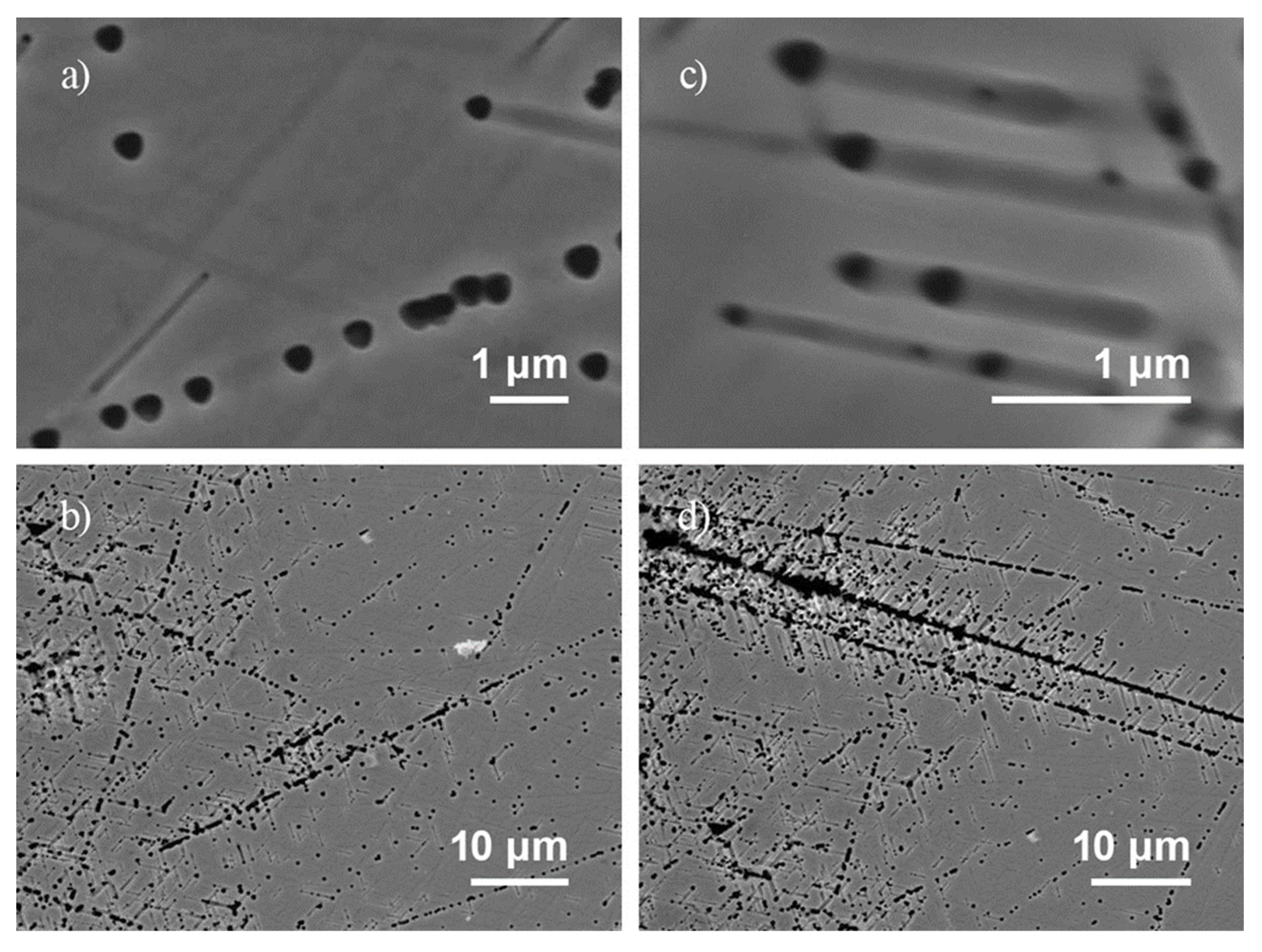
Figure 6.
SEM image of a porous surface of n-InP (111), showing the intersection of dissolution channels and tracks at an angle of 135°С.
Figure 6.
SEM image of a porous surface of n-InP (111), showing the intersection of dissolution channels and tracks at an angle of 135°С.
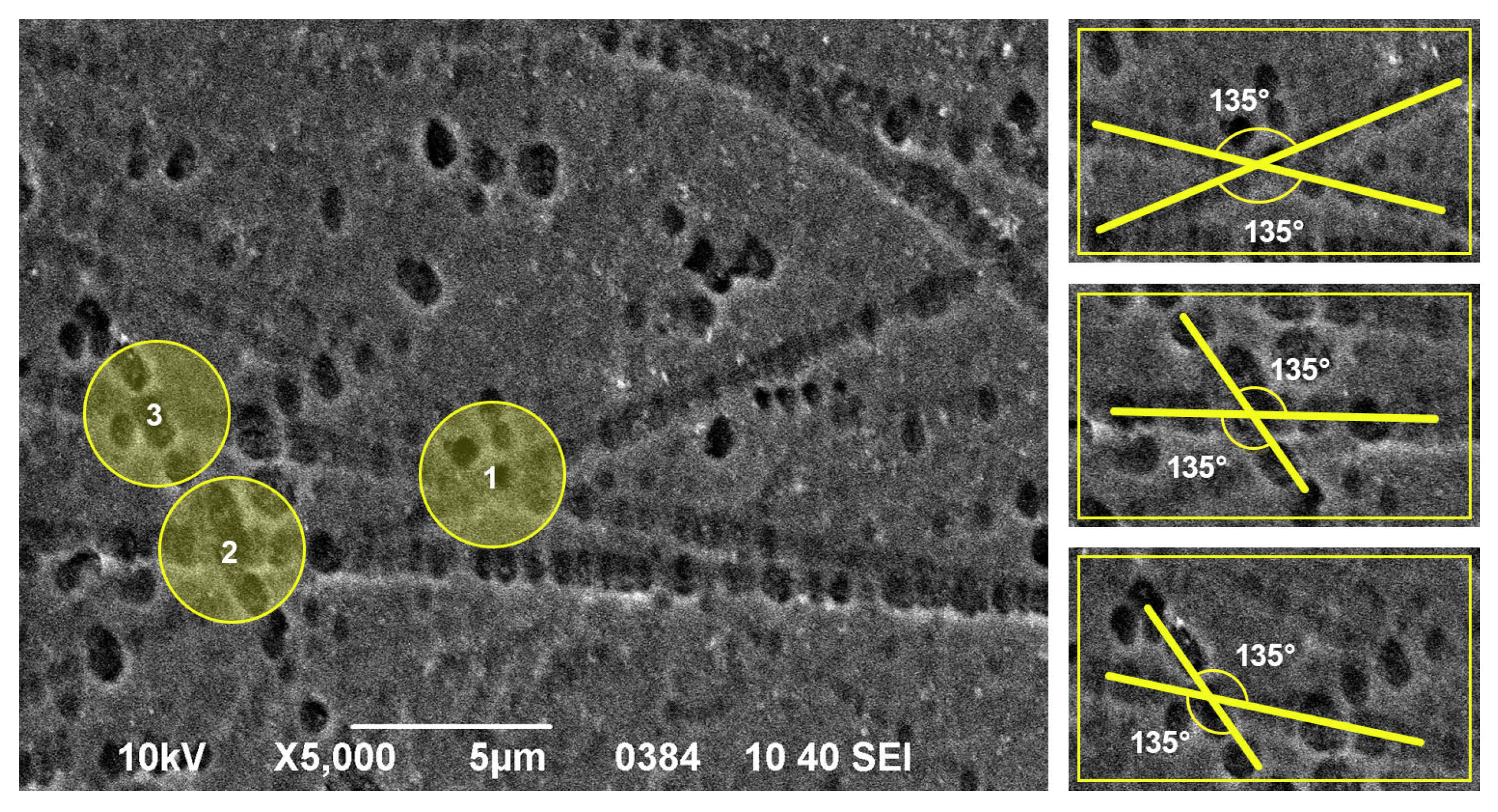
Figure 7.
SEM image of oxide crystallites of the parquet type on the surface of n-InP (111), formed during electrochemical etching.
Figure 7.
SEM image of oxide crystallites of the parquet type on the surface of n-InP (111), formed during electrochemical etching.
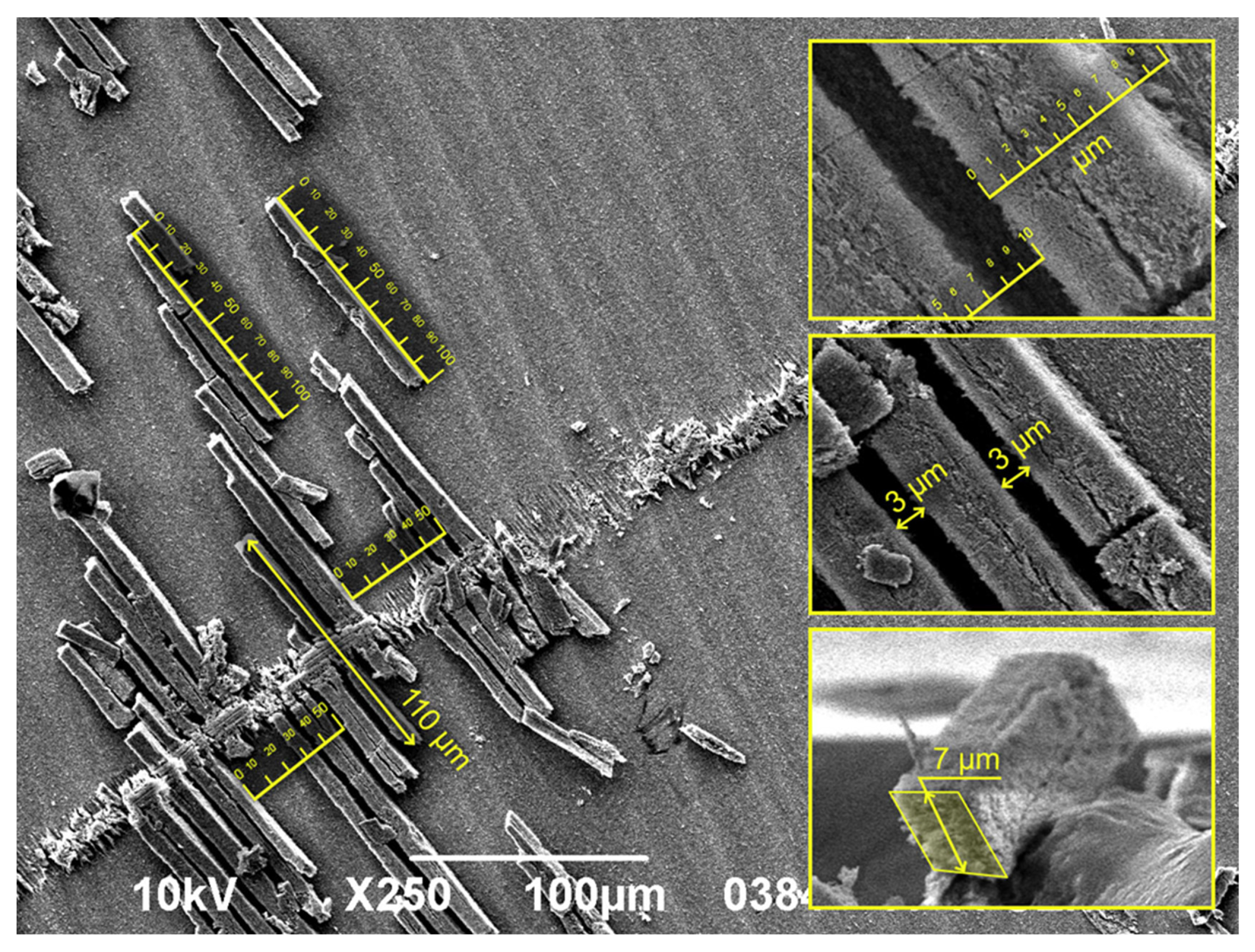
Figure 8.
Flower-like crystallites on the surface of indium phosphide, formed in areas of excessive impurity concentration (a, b, c) and schematic representation of a crystallite (d) on flat (e) and porous (f) surfaces at the semiconductor/electrolyte boundary SEM image of oxide crystallites of the parquet type on the surface of n-InP (111), formed during electrochemical etching.
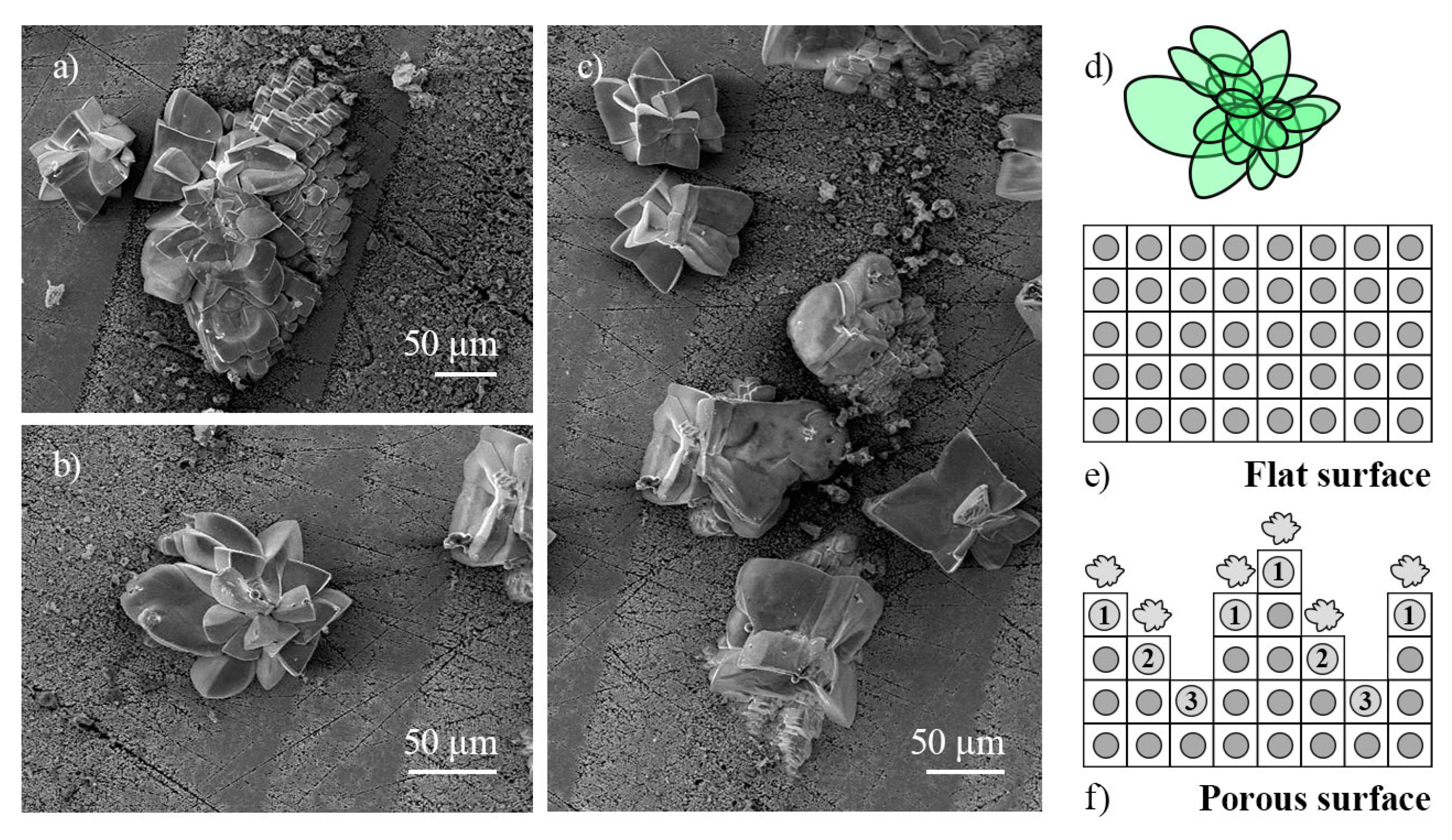

Table 1.
Samples for Experiment.
| Item | Specifications | |
|---|---|---|
| Conductivity type | n-type | p-type |
| Dopant | S | Zn |
| Carrier concentration | 2,3х1018 см-3 | |
| Orientation | (111), (100), (001) | |
| Crystal lattice | face-centered cubic (“zinc blende”) | |
| Mobility | (1.5-3.5)x103cm2/V.s | (50-70)×103cm2/V.s |
Disclaimer/Publisher’s Note: The statements, opinions and data contained in all publications are solely those of the individual author(s) and contributor(s) and not of MDPI and/or the editor(s). MDPI and/or the editor(s) disclaim responsibility for any injury to people or property resulting from any ideas, methods, instructions or products referred to in the content. |
© 2025 by the authors. Licensee MDPI, Basel, Switzerland. This article is an open access article distributed under the terms and conditions of the Creative Commons Attribution (CC BY) license (http://creativecommons.org/licenses/by/4.0/).
Copyright: This open access article is published under a Creative Commons CC BY 4.0 license, which permit the free download, distribution, and reuse, provided that the author and preprint are cited in any reuse.


