
Submitted:
28 July 2025
Posted:
29 July 2025
You are already at the latest version
Abstract
This article presents a compact model for the radiation sensitive field-effect transistor (RADFET). The model represents the basic IV-curve of the MOSFET device. Threshold voltage shift dependency on absorbed dose and gate bias, gate tunneling current, gate radiation current, dose accumulation and fading. The model represents the high-field effects in the gate dielectric of RADFET device. The Fowler-Nordheim gate tunneling current and radiation induced gate current are taken into account in the model. The model allows to determine the radiation induced charge during the RADFET operation under high-field injection mode. This improves the precision of the accumulated dose readout. The proposed model is ready for integration in any SPICE compatible circuit simulators. The presented compact model is able to represent any RADFET device including devices with high-k gate dielectrics. The model was designed exclusively using open-source circuit simulation tools.
Keywords:
MOSFET
; RADFET
; compact modeling
; circuit simulation
1. Introduction
Radiation sensitive field-effect transistors (RADFETs) are widely used for ionizing radiation control in areas such as aerospace equipment, nuclear setups, dosimetry equipment, radiation therapy, and environmental monitoring [1,2,3]. Usually, p-channel metal-oxide-semiconductor field effect transistors (PMOSFET) are used as the RADFET device. The radiation induced charge in the gate dielectric of the MOSFET device generates the threshold voltage shift [4,5,6]. It is possible to calibrate the shift dependency on the accumulated dose and determine the accumulated dose from the value readout [1,6,7]. RADFET sensors have many advantages such as small sensor area, low cost, and simple readout circuitry. It is possible to embed the RADFET sensor in the integration circuits (ICs) to set the device operating point and readout processing [8].
The improvement of the dose sensitivity and usage of the standard CMOS technology nodes such as CD4000 are the most important development directions for the RADFET sensors [9,10,11]. Usually such RADFET sensors operate at positive gate bias. This operation mode speeds up the separation of electron-hole pairs, which are generated under the device irradiation, and increases the radiation induced charge accumulated in the gate dielectric [12,13,14]. The dose sensitivity of the RADFET device and the charge work function increase with the electric field strength in the in the gate dielectric. The operation of MOS sensors under high fields in the gate dielectric and under the Fowler-Nordheim tunneling is especially interesting [15,16,17]. The usage of the high-field electrons tunneling allows to conduct the injection annealing after the irradiation [15,17,18]. Our research team proposed the model describing the charge processes in the MOS sensors under different gate bias up to high-field injection region [19,20]. The integration of the proposed mathematical model in the SPICE compatible circuit simulation software would improve its availability. The RADFET SPICE models would be especially useful for the specialized ICs design. The SPICE RADFET model could be also used for the design of radiation hardened ICs. It allows to take into account the shift of the MOSFET parameters under the influence of the irradiation.
SPICE-based circuit simulation tools [21] are the industrial standard for electronic circuits modelling. The most of proprietary (HSPICE, LTspice) and open source (Ngspice, Xyce) circuit simulation tools are based on original SPICE code developed by L.Nagel. The SPICE simulation kernel supports a set of basic passive and active primitive devices, including resistors, inductors, sources, and transistors. The electronic components not presented in a basic set of SPICE devices should be represented using macromodels or compact models [22]. The macro models represents a complex device as an equivalent circuit. The compact models differs from the macro model by the usage only of simple devices like controlled sources and RCL components in the equivalent circuit. The electronic components are represented by a set of equations describing the voltages and current at its terminals.
The RADFET device is not presented among the standard SPICE devices. There exists a need to develop a custom model for this device. This will allow to simulate the analog part of the dosimeter readout circuitry using SPICE compatible circuit simulation tools. The paper [23] presents a modification of the standard SPICE MOSFET model. The radiation input is represented as the subcircuit parameter. This approach has some limitations and uses only a simplified dependency of the MOSFET threshold voltage shift on the absorbed dose. The purpose of this research is to extend the model presented in [23] and to add supplementary effects like gate tunneling current, threshold voltage shift under irradiation, and fading. It is important for the simulation of analog circuits containing RADFET devices. The research [24] presents a limited compact model of the RADFET device, but provides no details on its implementation.
The rest of the paper is organized as the following. The Section 2 provides an overview of the RADFET device, software used for the model generation, and model equations. The Section 3 presents the structure of the generated SPICE model and compares the data from simulation and measurement. The Section 4 gives a model usage example for readout circuit design. The Section 5 gives an outcome of the paper and the summary of the achieved results.
2. Materials and Methods
2.1. Used RADFET Device
The RADFET devices [19] were fabricated using the 6 um CMOS technology compatible with CD4000 logic IC series. The topology of the RADFET is shown in the Figure 1. It is PMOS device with channel length um and channel width um. The n-type silicon wafer doped by phosphorus was used as the substrate. The substrate has 4.5 Ohms per square resistance and <100> orientation. The gate dielectric is silicon dioxide with 100 nm thickness. The total device area is 1600000 um². The layout view of the RADFET device is shown in the Figure 2.
2.2. Circuit Simulation Software
The Qucs-S (developed by Kuznetsov et al. [25]) open source circuit simulator was used for design of the presented compact model. This tool has the following advantages. It is free and open-source and has advanced features for debugging of the compact models. Qucs-S uses free Ngspice [26] simulation kernel that is fully compatible with proprietary SPICE tools. Internal Verilog-A synthesizer of Qucs-S allows to export the designed compact model to Verilog-A module. Interactive tuning and optimization tools implemented in Qucs-S GUI level allow to perform models parameters extraction. The key feature of Qucs-S is the quick switching between the simulation backends while the program operation. Qucs-S uses external simulation kernel Ngspice [27] and Verilog-A [28] modules compiler OpenVAF. The data flow diagram is shown in the Figure 3. It illustrates the interaction between the parts of the simulation software package.
2.3. Basic RADFET Model Equations
The most of RADFET deices are fabricated using the micron technology. And the drain current could be described by MOSFET level 1 equations. The higher levels MOSFET models and BSIM models [29] are applicable for submicron devices and have no benefit for RADFET. The drain current depends on the voltages between the MOSFET pins: gate to source and and drain to source .
The drain current in the linear IV-curve region ():
where the is a threshold voltage (V), – channel modulation (1/V); – transconductance ();
The drain current in the saturation region if :
The source of the RADFET device is internally connected to bulk. The source-bulk voltage . Therefore the threshold voltage dependency on bulk potential may not be taken into account.
The threshold voltage and device transconductance have dependency on the device absolute temperature T (K) that must be taken into account in the module. The threshold voltage dependency may be approximated by linear function:
where the is the temperature where the initial device parameters could be measured and is a temperature coefficient (V/K). The transconductance temperature dependency may be approximated by the power function:
where is a coefficient varying in range from 1.3 to 1.5.
2.4. Radiation Dependency of the Threshold Voltage
The threshold voltage of the MOSFET is linear dependent on the absorbed dose D. The basic model may assume a simple linear dependency of the threshold voltage shift on absorbed dose (expressed in rads or Gy). We will use the rads as the dose units further in paper.
The S is a sensitivity coefficient expressed in . The saturation of the threshold voltage shift at the higher dose may be expressed with a hyperbolic tangent. The more precise approximation proposed in [4,30] may cause convergence issues with SPICE simulator.
where is a dose at which saturation is reached. Usually rad.
The sensitivity has a dependency on gate bias during irradiation [31]:
where the and are the fitting coefficient. If the only the linear dependency on dose is taken into account.
2.5. Gate Current Model
The both MOSFET level 1-9 and BSIM model do not take into account gate current and radiation effects on gate current. The gate current could be normalized to gate current density and gate area:
The gate current density of the RADFET device consists of three components: capacitive current , high-field tunnel injection current , and radiation current .
capacitive component could be expressed using the known unity gate capacitance which may be expressed from gate dielectric parameters and gate oxide thickness :
where is a gate dielectric (for example SiO2) permittivity and is a dielectric constant.
The injection current could be expressed using the Fowler-Nordheim equations:
where is a barrier potential (V); and are Fowler-Nordheim tunneling constants.
The radiation current is expressed by the following equation [19]:
where q is the charge of electron, is a value of electron-hole pair per dose unit and SiO2 volume (). The is the charge yield under irradiation. It depends on the field E in the gate dielectric. It could be determined from the data provided by Schwank et al. [13]. We use the following approximation in the compact model:
where the and are the fitting constants depending on radiation type (gamma-ray, protons, etc.). The plots of the approximation function are shown in the Figure 4. It shows good match with experimental plots from [13]
3. Results
3.1. The Equivalent Circuit of the RADFET Device
The compact model represented by the following equivalent designed in Qucs-S is shown in the Figure 5.
The equivalent circuit consists of a number of behavioral current and voltage sources and equation defined passive devices. The model has three terminals for MOSFET electrodes: gate (G), source (S), drain (D), and the fourth terminal (RAD) serving as the virtual radiation input. The voltage source representing the absorbed dose in rads should be connected to this terminal. The B1 source represents the drain current level 1 MOSFET model with equations (1) and (2). The B2 source is responsible for transconductance temperature dependency (4). The B3 and B4 current sources represent the gate injection (12) and radiation (13) currents respectively. The capacitor C1 is the gate capacitance (11). The L1 inductor and B5 source are a differentiation stage and serve to obtain the radiation intensity using the fundamental properties of inductor current. The B6 controlled source represents a threshold voltage shift dependency on the absorbed dose taking into account gate bias. It relates to equation (7).
The model parameters are summarized in the Table 1. This table provides parameter default value, desciption, and unit.
Qucs-S allows to export the schematic representation of the compact model to a SPICE netlist. The SPICE code synthesized from the model is shown in the Listing 1.
| Listing 1. SPICE code of the RADFET model |
|
.SUBCKT RADFET_PMOS S D G RAD Vt0=-2.0 Kp=1e-4 + L=1u W=1u lambda=1e-5 S1=1.5e-3 + Tox=100e-9 Tnom=26.85 TCVTH=2e-3 Mu=1.5 + Dsat=1e6 S2=0.0 VG=0.0 .PARAM eps0=8.854e-12 .PARAM eps=3.9 .PARAM Area=L*W .PARAM phiB=3.1 .PARAM A=1.54e-6*(1/phiB) .PARAM B=6.83e7*(phiB**1.5)*(0.5**0.5) .PARAM q=1.6e-19 .PARAM Ye=0.8 .PARAM Kg=8e12 .PARAM ToxCM=Tox*100 .PARAM AreaCM2=Area*1e4 .PARAM Esat=1e6 .PARAM Yem=1.0 R1 0 RAD 1E12 tc1=0.0 tc2=0.0 C1 S G {EPS*EPS0*L*W/TOX} B1 S D I = (V(G,S)>(V(Vt0)))? + 0:((V(D,S)>(V(G,S)-(V(Vt0))))?(W/L)*V(Kp)* + (1-lambda*V(D,S))*(V(G,S)-V(D,S)/2-(V(Vt0)))*V(D,S): + (W/(2*L))*V(Kp)*(V(G,S)-(V(Vt0))) + *(V(G,S)-(V(Vt0)))*(1-lambda*V(D,S))) B2 kp 0 V = Kp*((Tnom+273)/(TEMPER+273))**Mu L1 0 DradDt 1 B5 0 DradDt I = V(rad) B3 G S I = A*((V(G,S)/ToxCM)**2)* + exp(-B/(abs(V(G,S))/ToxCM))*AreaCM2*sgn(V(G,S)) B6 Vt0 0 V = Vt0-(S1-S2*exp(-abs(V(g,s))/3.1))* + Dsat*tanh(v(rad)/Dsat)+TCVTH*(TEMPER-Tnom) B4 G S I = q*Kg*ToxCM*(V(DradDt))*AreaCM2* + Yem*tanh(abs(V(G,S)/ToxCM/Esat)) .ENDS |
3.2. Equivalent Circuit Representing Dose Accumulation and Fading
The fading [30] shows the decay of the threshold voltage shift after the irradiation:
where is the threshold voltage after the irradiation, is the threshold voltage after time T, and is the threshold voltage without irradiation.
3.3. IV-Curves Simulation
The , , and are the MOSFET level 1 model parameters. Its extraction procedure is well described in the literature and not considered here. The pair of and curves are required. The used RADFET device is compatible with the CD4000 technology and these parameters could be taken from the basic technology.
The temperature dependency parameters and are extracted from fitting of the zero temperature coefficient point at the – curves family at different temperatures within the device operation range. The modeled ZTC point should match the measured ZTC point.
An example of the temperature parameters extraction is shown in the Figure 7. The ZTC point for the used device achieved at the drain current .
3.4. Sensitivity Simulation
The sensitivity extraction requires I-V curves measurement under different irradiation level. We have measured the curves for three irradiation doses: 7 krad, 10 krad and 15 krad with no bias applied at gate. This data was used for sensitivity extraction. The testbench schematic in Qucs-S is shown in the Figure 8. The V3 voltage source represents the absorbed dose input. The voltage at this terminal is equal to the dose in rads.
The simulated and measured I-V curves are shown in the Figure 9. The measurements were taken without radiation and under radiation levels 7 krad, 10 krad, and 15 krad. The gamma-ray 60Co source was used.
3.5. Gate Bias Dependency of Sensitivity
The sensitivity could be extracted from SPICE simulation as the derivative of the threshold voltage:
The threshold voltage could be measured if the MOSFET drain and gate are connected to current source and the source is connected to ground. If the source current is in microampere range, the voltage at the drain node will be nearly equal to threshold voltage. The testbench schematic and sensitivity extraction script are shown in the Figure 10
The simulation results are shown in the Figure 11. The data for IRF9520 power MOSFET provided in the paper [4] was used, because the dependency on the gate bias for the device described in the Section 2.1 was not measured. The , , and parameters for this MOSFET were taken from the SPICE VDMOS model. The simulation shows a good match with the measurement data. The extracted parameters are the following: mV/rad, mV, V.
3.6. Gate Current Simulation
The testbench schematic for the gate current simulation is shown in the Figure 12. The DC injection current source I1 is connected to the MOSFET gate. All other electrodes are grounded. The V1 pulsed source represents a virtual radiation beam. The gate voltage drop is controlled at the transient simulation.
The Figure 13 shows the simulation result for the testcase described in the paper [20]. The MOS sensor (RADFET) was injected by current density A/cm². Then it was irradiated by gamma-rays to achieve the radiation current density higher than injection current density. The voltage drop on the MOS structure (RADFET) depends on the ratio of the radiation current and total current. The simulation shows a good match with the data provided in [20].
4. Discussion
The designed compact model allows to simulate the input stage of the dosimeter [32] and its analog harness. The dosimeter input schematic is shown in the Figure 14. The LM334 current source IC REF1 provides the constant current at the drain. The S1 and S2 switches serve to simulate the irradiation phase and measurement phase. The V1 pulsed source is the virtual radiation input. At the starting time the S1 is closed and S2 is open. All electrodes of the RADFET are connected to ground and the sensor is under the irradiation. When the radiation phase ends, the S1 opens and S2 closes and MOSFET is switched to the measurement circuit. The drain voltage is nearly equal to the threshold voltage.
The simulated output voltage and input radiation dose are shown in the Figure 15. The voltage at the drain is nearly , because the dose does not approach the saturation dose and no gate bias is applied at the irradiation phase.
5. Conclusions
The compact model of the RADFET device was presented in this paper. The developed model extends the SPICE MOSFET models and allows to simulate the following effects:
- basic MOSFET IV-curve dependency;
- threshold voltage shift dependency on the adsorbed does and gate bias at the irradiation phase;
- tunneling gate current and irradiation gate current;
- threshold voltage fading after the irradiation.
The model parameters could be extracted from IV-curve measurements and threshold voltage shift measurements at the irradiation. The developed compact model is compatible with open-source and proprietary SPICE circuit simulation kernels.
Author Contributions
Conceptualization, V.A. and A.I.P.; Funding acquisition, V.A.; Investigation, V.K. and D.A., Software, V.K.; Methodology, V.K. and D.A.; Supervision, V.A. and A.I.P.; Visualization, S.P.; Writing – Original Draft preparation, V.K., D.A., and S.P., Writing – Review and editing, V.K. and D.A. All authors have read and agreed to the published version of the manuscript.
Funding
The research was financially supported by the Ministry of Science and Higher Education of the Russian Federation as a part of the project FSFN-2024-0086
Data Availability Statement
We encourage all authors of articles
Conflicts of Interest
The authors declare no conflicts of interest.
References
- Holmes-Siedle, A.; Adams, L. RADFET: A review of the use of metal-oxide-silicon devices as integrating dosimeters. International Journal of Radiation Applications and Instrumentation. Part C. Radiation Physics and Chemistry 1986, 28, 235–244. [CrossRef]
- Kulhar, M.; Dhoot, K.; Pandya, A. Gamma Dose Rate Measurement Using RadFET. IEEE Transactions on Nuclear Science 2019, 66, 2220–2228. [CrossRef]
- Camanzi, B.; Holmes-Siedle, A.G. The race for new radiation monitors. Nature Materials 2008, 7, 343–345. [CrossRef]
- Ristić, G.S.; Ilić, S.D.; Veljković, S.; Jevtić, A.S.; Dimitrijević, S.; Palma, A.J.; Stanković, S.; Andjelković, M.S. Commercial P-Channel Power VDMOSFET as X-ray Dosimeter. Electronics 2022, 11. [CrossRef]
- Assaf, J. Characterization of Commercial P-MOSFETs for Using as a Gamma-Rays Dosimeter. Silicon 2022, 14, 1767–1774. [CrossRef]
- Pejovic, M.M. Application of p-Channel Power VDMOSFET as a High Radiation Doses Sensor. IEEE Transactions on Nuclear Science 2015, 62, 1905–1910. [CrossRef]
- Andjelković, M.S.; Ristić, G.S.; Jakšić, A.B. Using RADFET for the real-time measurement of gamma radiation dose rate. Measurement Science and Technology 2015, 26, 025004. [CrossRef]
- Ravotti, F. Dosimetry Techniques and Radiation Test Facilities for Total Ionizing Dose Testing. IEEE Transactions on Nuclear Science 2018, 65, 1440–1464. [CrossRef]
- Siebel, O.; Pereira, J.; Souza, R.; Ramirez-Fernandez, F.; Schneider, M.; Galup-Montoro, C. A very-low-cost dosimeter based on the off-the-shelf CD4007 MOSFET array for in vivo radiotherapy applications. Radiation Measurements 2015, 75, 53–63. [CrossRef]
- Ristić, G.S.; Vasović, N.D.; Kovačević, M.; Jakšić, A.B. The sensitivity of 100nm RADFETs with zero gate bias up to dose of 230Gy(Si). Nuclear Instruments and Methods in Physics Research Section B: Beam Interactions with Materials and Atoms 2011, 269, 2703–2708. [CrossRef]
- Pejović, M.M.; Pejović, S.M. VDMOSFET as a prospective dosimeter for radiotherapy. Applied Radiation and Isotopes 2018, 132, 1–5. [CrossRef]
- Ristic, G.S.; Ilic, S.D.; Andjelkovic, M.S.; Duane, R.; Palma, A.J.; Lalena, A.M.; Krstic, M.D.; Jaksic, A.B. Sensitivity and fading of irradiated RADFETs with different gate voltages. Nuclear Instruments and Methods in Physics Research Section A: Accelerators, Spectrometers, Detectors and Associated Equipment 2022, 1029, 166473. [CrossRef]
- Schwank, J.R.; Shaneyfelt, M.R.; Fleetwood, D.M.; Felix, J.A.; Dodd, P.E.; Paillet, P.; Ferlet-Cavrois, V. Radiation Effects in MOS Oxides. IEEE Transactions on Nuclear Science 2008, 55, 1833–1853. [CrossRef]
- Oldham, T.; McLean, F. Total ionizing dose effects in MOS oxides and devices. IEEE Transactions on Nuclear Science 2003, 50, 483–499. [CrossRef]
- Lipovetzky, J.; Holmes Siedle, A.; Garcia Inza, M.; Carbonetto, S.; Redin, E.; Faigon, A. New Fowler-Nordheim Injection, Charge Neutralization, and Gamma Tests on the REM RFT300 RADFET Dosimeter. IEEE Transactions on Nuclear Science 2012, 59, 3133–3140. [CrossRef]
- Andreev, D.V.; Andreev, V.V.; Konuhova, M.; Popov, A.I. Technique of High-Field Electron Injection for Wafer-Level Testing of Gate Dielectrics of MIS Devices. Technologies 2024, 12. [CrossRef]
- Peng, L.; Hu, D.; Jia, Y.; Wu, Y.; An, P.; Jia, G. Analysis on the Rapid Recovery of Irradiated VDMOSFETs by the Positive High Electric Field Stress. IEEE Transactions on Nuclear Science 2017, 64, 2633–2638. [CrossRef]
- Andreev, D.V.; Bondarenko, G.G.; Andreev, V.V. Change in the Charge State of MOS Structures with a Radiation-Induced Charge under High-Field Injection of Electrons. Journal of Surface Investigation: X-ray, Synchrotron and Neutron Techniques 2023, 17, 48–53. [CrossRef]
- Andreev, D.V.; Bondarenko, G.G.; Andreev, V.V.; Stolyarov, A.A. Use of High-Field Electron Injection into Dielectrics to Enhance Functional Capabilities of Radiation MOS Sensors. Sensors 2020, 20. [CrossRef]
- Andreev, V.V.; Bondarenko, G.G.; Andreev, D.V.; Stolyarov, A.A. Use of MIS Sensors of Radiation in High-Field Electron Injection Modes. Journal of Contemporary Physics (Armenian Academy of Sciences) 2020, 55, 144–150. [CrossRef]
- Vladirmirescu, A. Shaping the History of SPICE. IEEE Solid-State Circuits Magazine 2011, 3, 36–39. [CrossRef]
- De Graaff, H.C.; Kloosterman, W.J.; Versleyen, M. Compact Modelling for Analoge Circuit Design. In Proceedings of the ESPRIT ’90, Dordrecht, 1990; pp. 65–76.
- Marjanović, M.; Ilić, S.D.; Veljković, S.; Mitrović, N.; Gurer, U.; Yilmaz, O.; Kahraman, A.; Aktag, A.; Karacali, H.; Budak, E.; et al. The SPICE Modeling of a Radiation Sensor Based on a MOSFET with a Dielectric HfO2/SiO2 Double-Layer. Sensors 2025, 25. [CrossRef]
- Mrozovskaya, E.; Zimin, P.; Chubunov, P.; Zebrev, G. Compact modeling of electrical characteristics of p-MNOS based RADFETs. In Proceedings of the International Conference on Micro- and Nano-Electronics 2018; Lukichev, V.F.; Rudenko, K.V., Eds. International Society for Optics and Photonics, SPIE, 2019, Vol. 11022, p. 110220I. [CrossRef]
- Brinson, M.; Kuznetsov, V. Qucs-0.0.19S: A new open-source circuit simulator and its application for hardware design. In Proceedings of the 2016 International Siberian Conference on Control and Communications (SIBCON), 2016, pp. 1–5. [CrossRef]
- Grabinski, W.; Scholz, R.; Verley, J.; Keiter, E.R.; Vogt, H.; Warning, D.; Nenzi, P.; Lannutti, F.; Salfelder, F.; Davis, A.; et al. FOSS CAD for the Compact Verilog-A Model Standardization in Open Access PDKs. In Proceedings of the 2024 8th IEEE Electron Devices Technology & Manufacturing Conference (EDTM), 2024, pp. 1–3. [CrossRef]
- Lannutti, F.; Nenzi, P.; Olivieri, M. KLU sparse direct linear solver implementation into NGSPICE. In Proceedings of the Proceedings of the 19th International Conference Mixed Design of Integrated Circuits and Systems - MIXDES 2012, 2012, pp. 69–73.
- Kuthe, P.; Müller, M.; Schröter, M. VerilogAE: An Open Source Verilog-A Compiler for Compact Model Parameter Extraction. IEEE Journal of the Electron Devices Society 2020, 8, 1416–1423. [CrossRef]
- Chauhan, Y.S.; Venugopalan, S.; Paydavosi, N.; Kushwaha, P.; Jandhyala, S.; Duarte, J.P.; Agnihotri, S.; Yadav, C.; Agarwal, H.; Niknejad, A.; et al. BSIM compact MOSFET models for SPICE simulation. In Proceedings of the Proceedings of the 20th International Conference Mixed Design of Integrated Circuits and Systems - MIXDES 2013, 2013, pp. 23–28.
- Ristic, G.S.; Ilic, S.D.; Duane, R.; Andjelkovic, M.S.; Palma, A.J.; Lallena, A.M.; Krstic, M.D.; Stankovic, S.J.; Jaksic, A.B. Radiation sensitive MOSFETs irradiated with various positive gate biases. Journal of Radiation Research and Applied Sciences 2021, 14, 353–357. [CrossRef]
- Pejović, M.M. Dose response, radiation sensitivity and signal fading of p-channel MOSFETs (RADFETs) irradiated up to 50Gy with 60Co. Applied Radiation and Isotopes 2015, 104, 100–105. [CrossRef]
- Vasović, N.D.; Ristić, G.S. A new microcontroller-based RADFET dosimeter reader. Radiation Measurements 2012, 47, 272–276. [CrossRef]
Figure 1.
Radiation sensor containing two PMOS RADFET devices
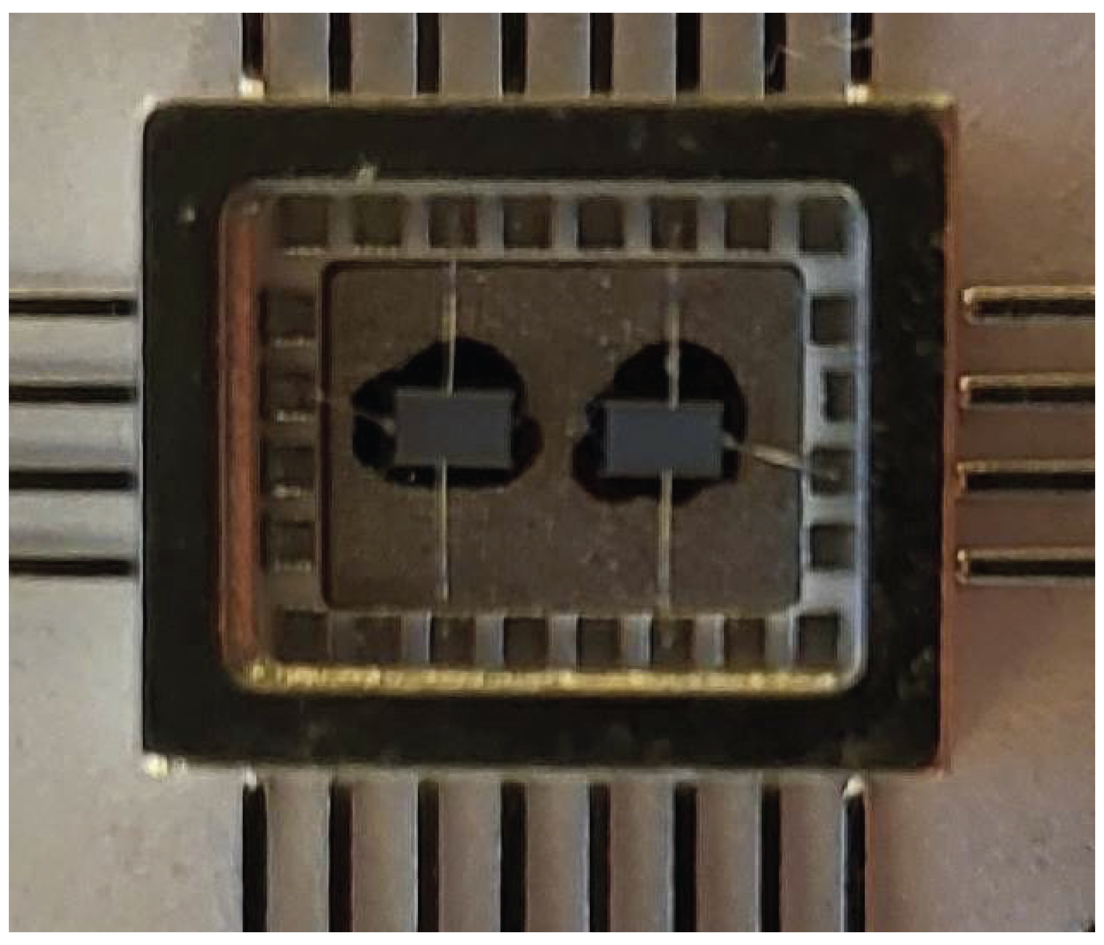
Figure 2.
RADFET device layout view
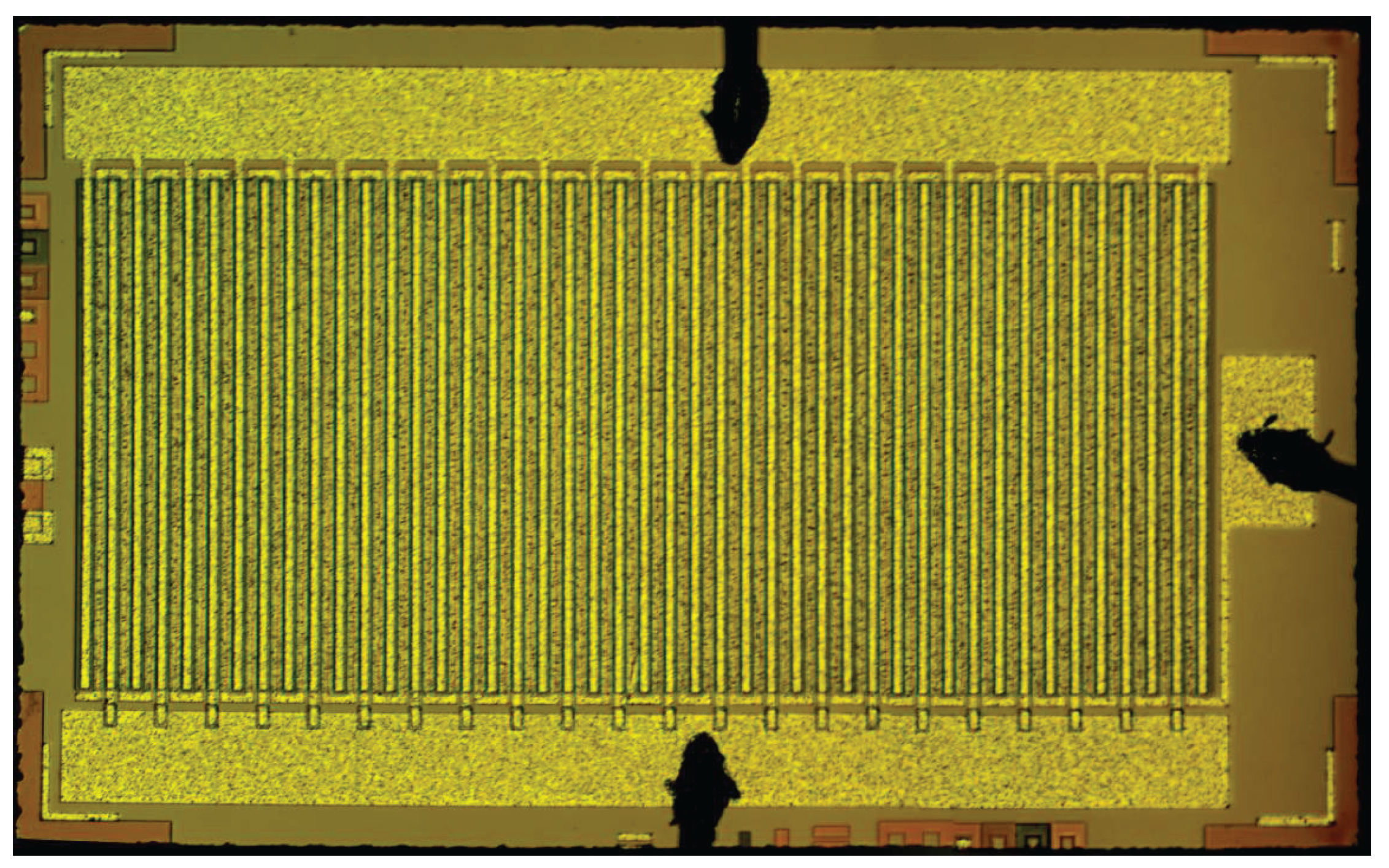
Figure 3.
Qucs-S dataflow diagram
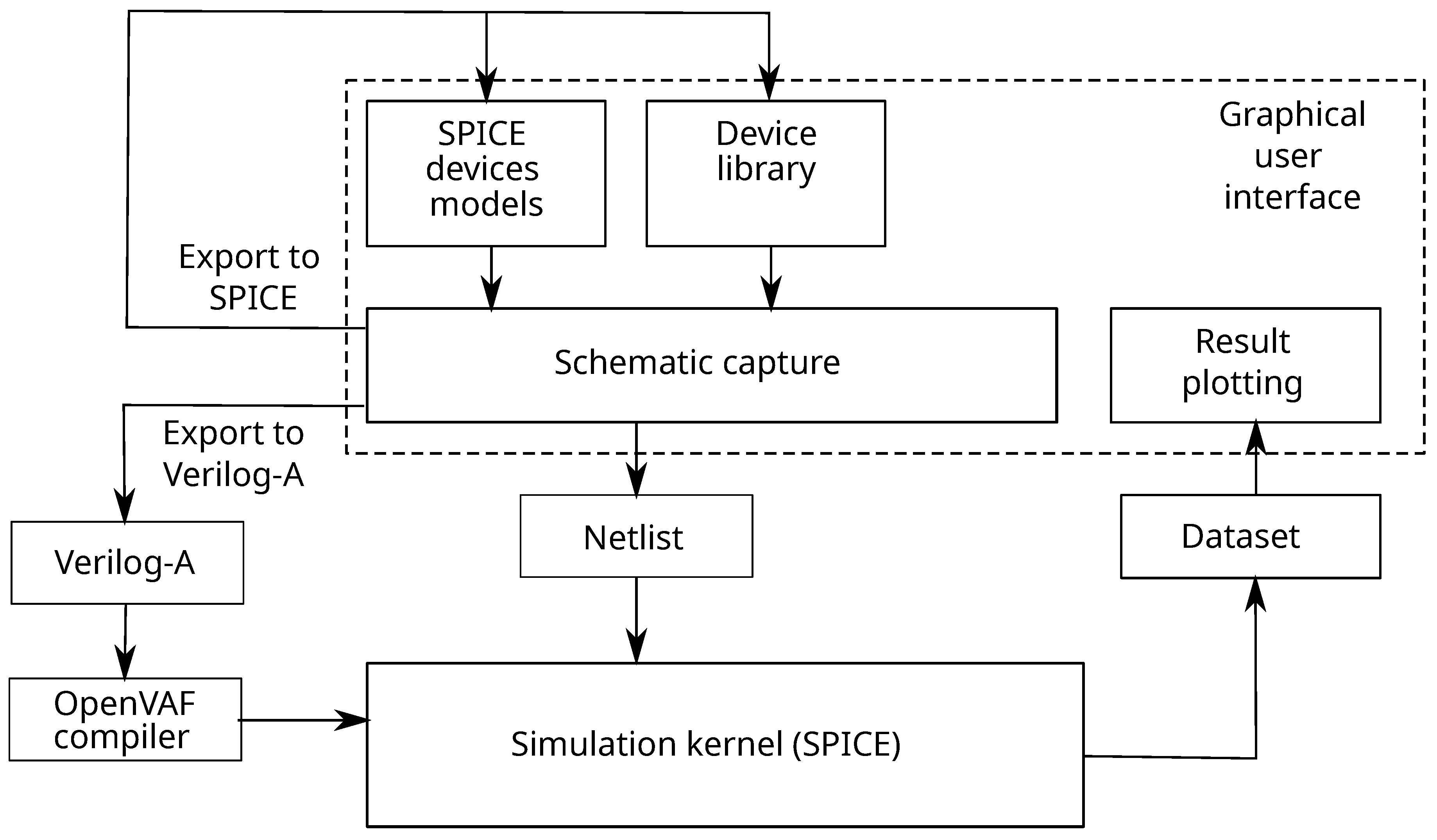
Figure 4.
Charge yield approximation
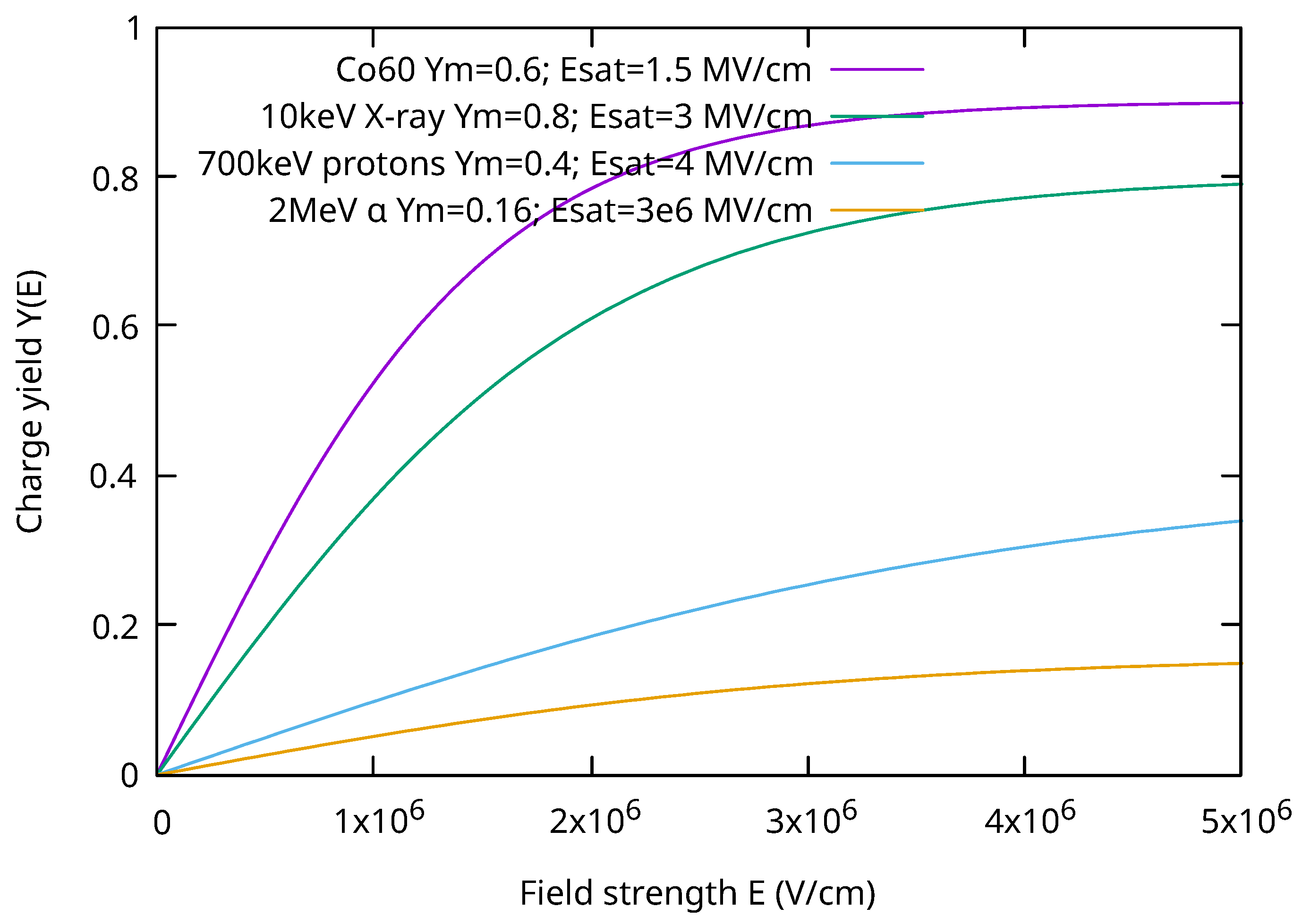
Figure 5.
The equivalent circuit representing the RADFET compact model

Figure 6.
The RC stage representing fading and charge accumulation
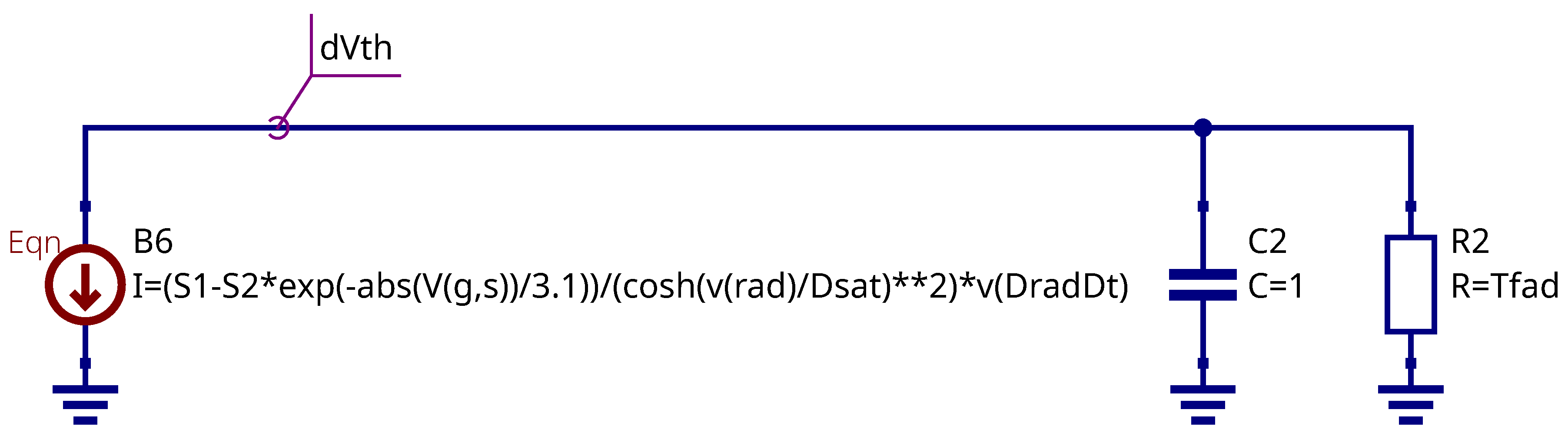
Figure 7.
Temperature dependency extraction of RADFET device
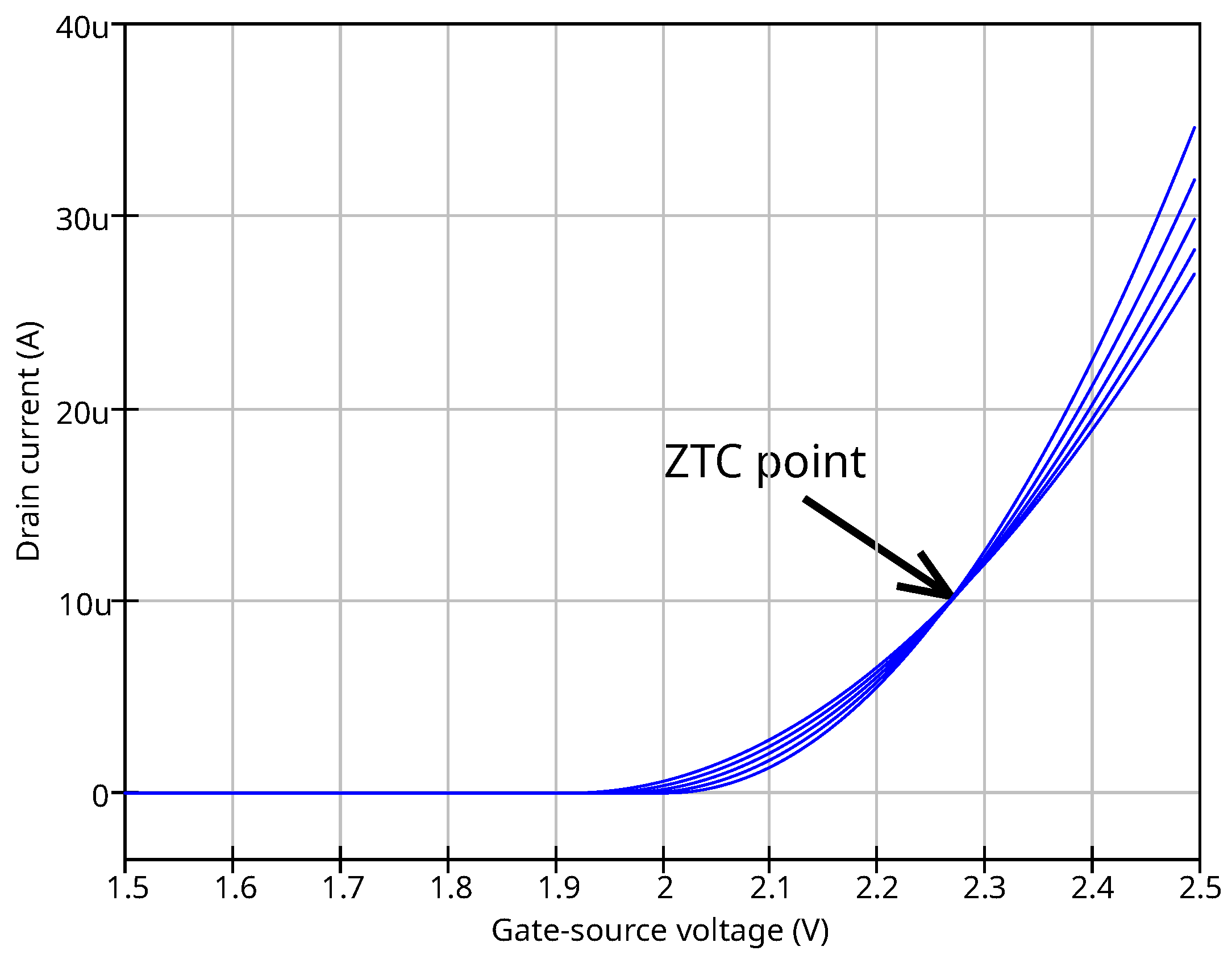
Figure 8.
Testbench schematic for I-V curves measurement
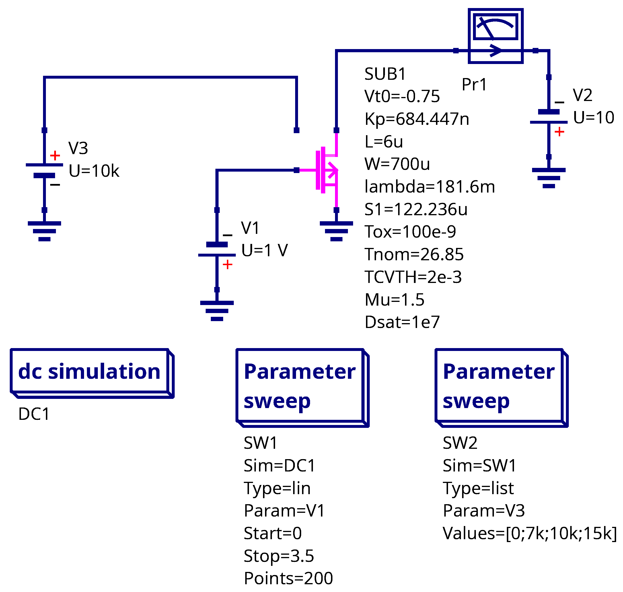
Figure 9.
Simulated (solid line) and measured (stars) I-V curves for the RADFET device
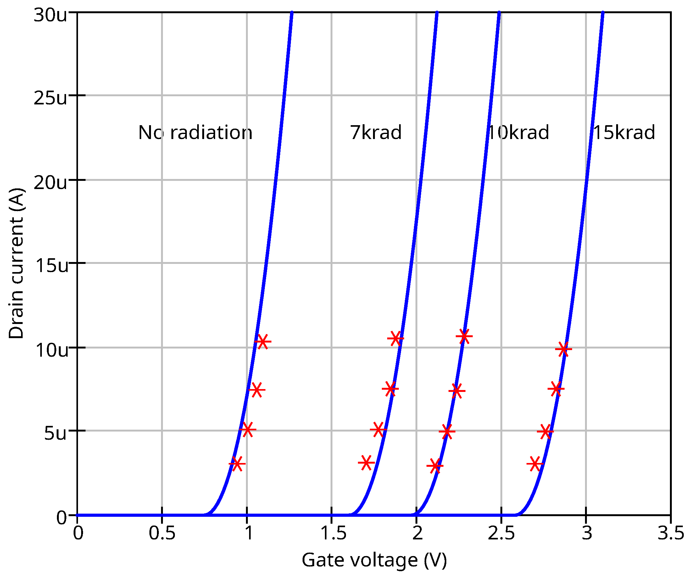
Figure 10.
Testbench schematic for sensitivity extraction
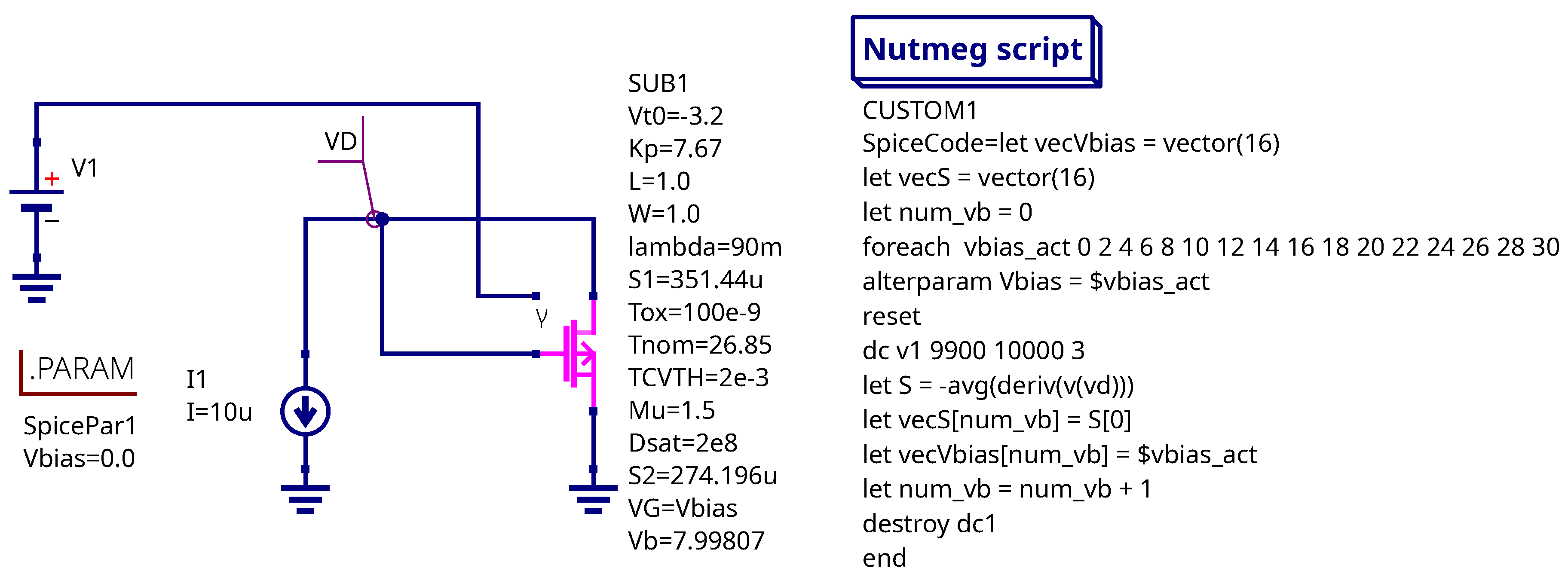
Figure 11.
Simulated (solid line) and measured (stars) sensitivity dependency on the gate bias
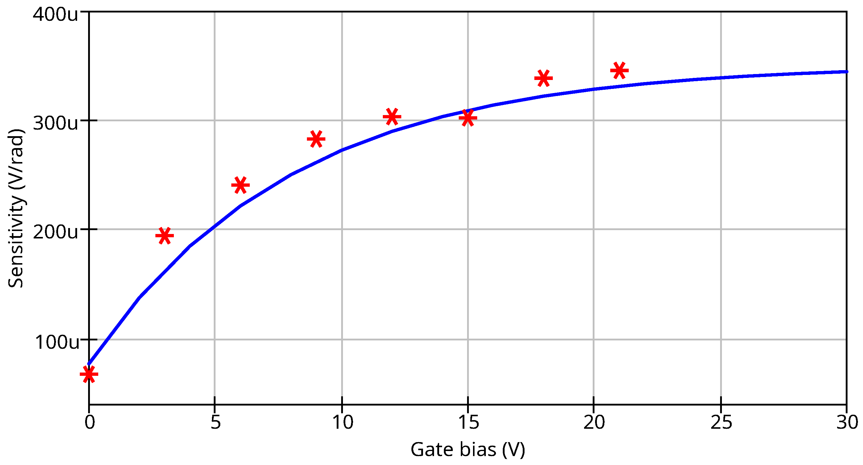
Figure 12.
Testbench schematic for the gate current simulation
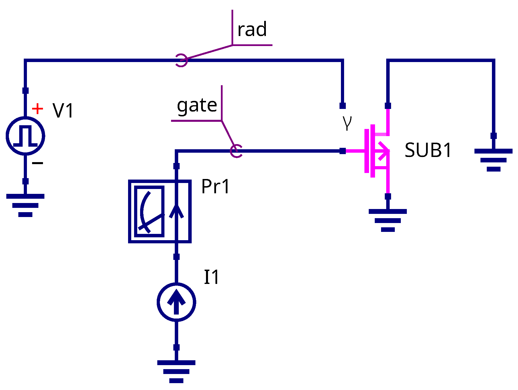
Figure 13.
Waveform of the voltage at RADFET gate under injection and irradiation. 1 – ; 2 – ; 3 – ; 4 – ;
Figure 13.
Waveform of the voltage at RADFET gate under injection and irradiation. 1 – ; 2 – ; 3 – ; 4 – ;
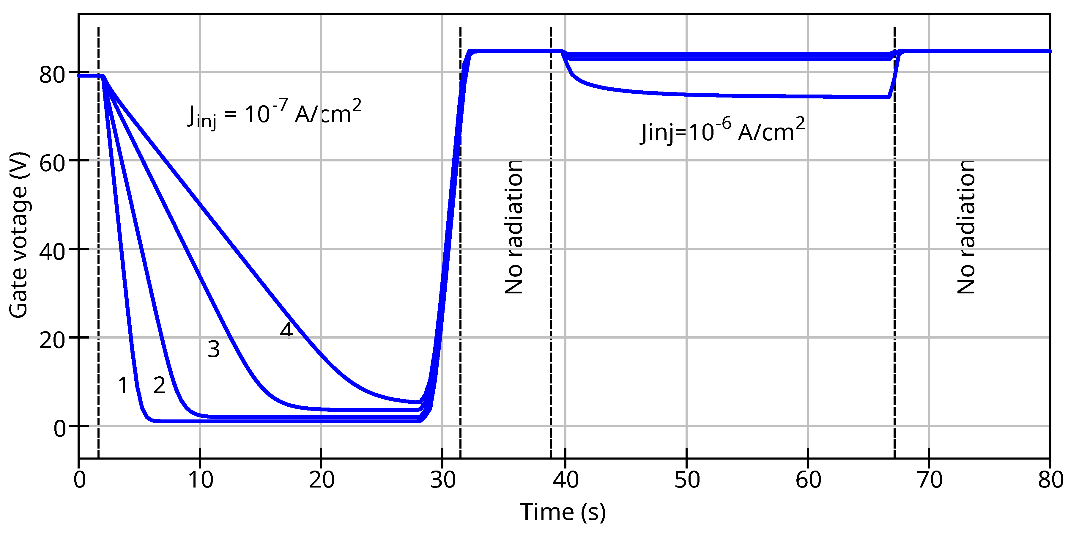
Figure 14.
The shematic of the dosimeter input designed in Qucs-S
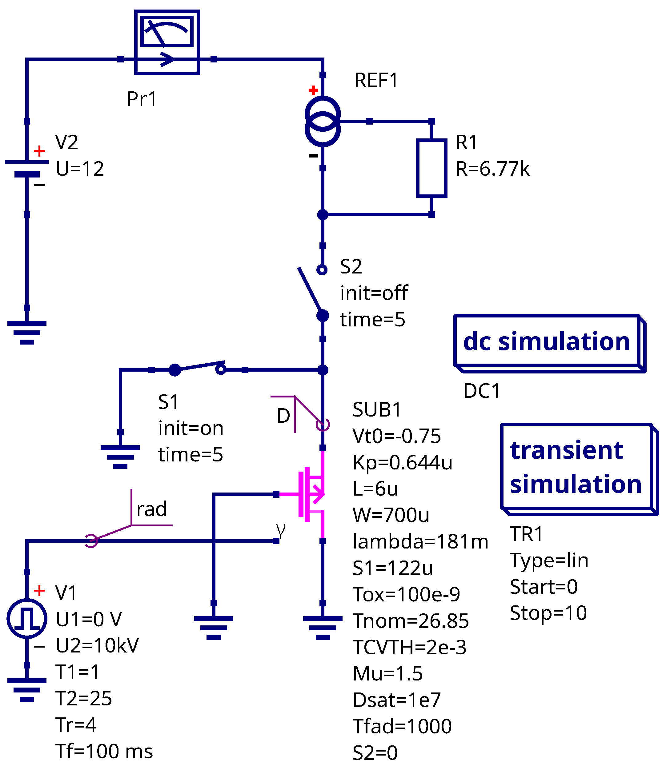
Figure 15.
The simulated output voltage of the dosimeter (dashed curve. left Y-axis) and accumulated dose (solid curve, right Y-axis))
Figure 15.
The simulated output voltage of the dosimeter (dashed curve. left Y-axis) and accumulated dose (solid curve, right Y-axis))
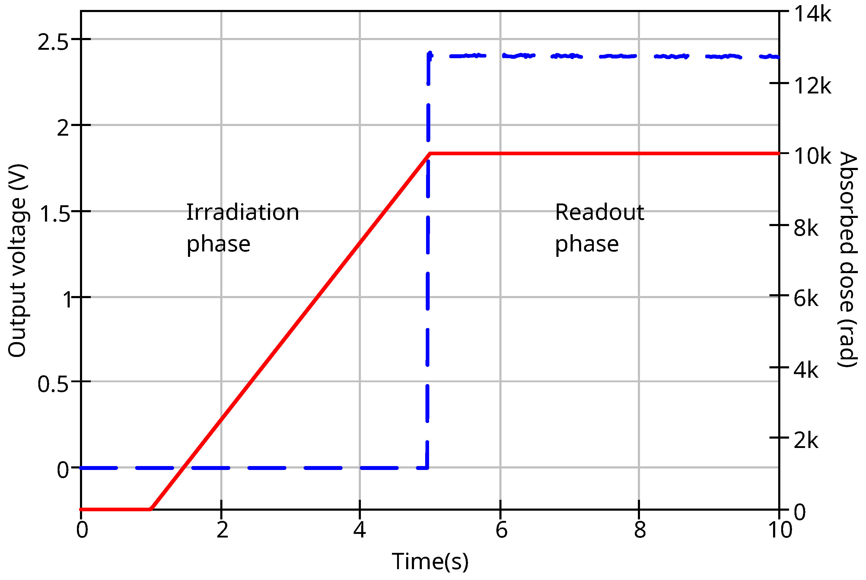

Table 1.
RADFET model parameters
| Model parameter | Default value | Unit | Description |
|---|---|---|---|
| -1.0 | V | Threshold voltage at no radiation | |
| A/V² | Transconductance | ||
| 1/V | Channel modulation | ||
| L | 1.0 | m | Device length |
| W | 1.0 | m | Device width |
| m | Gate dielectric thickness | ||
| 3.9 | Gate dielectric relative permittivity | ||
| 1e-3 | V/K | Threshold voltage temperature coefficient | |
| 1.5 | Transconductance temperature coefficient | ||
| 0.0015 | V/rad | Linear sensitivity component | |
| 0.0 | V | Exponential sensitivity | |
| 3.0 | V | Exponential sensitivity fitting coefficient | |
| 0.0 | V | Gate bias at the irradiation time | |
| rad | Saturation dose | ||
| 26.85 | °C | temperature at which device parameters were measured |
Disclaimer/Publisher’s Note: The statements, opinions and data contained in all publications are solely those of the individual author(s) and contributor(s) and not of MDPI and/or the editor(s). MDPI and/or the editor(s) disclaim responsibility for any injury to people or property resulting from any ideas, methods, instructions or products referred to in the content. |
© 2025 by the authors. Licensee MDPI, Basel, Switzerland. This article is an open access article distributed under the terms and conditions of the Creative Commons Attribution (CC BY) license (http://creativecommons.org/licenses/by/4.0/).
Copyright: This open access article is published under a Creative Commons CC BY 4.0 license, which permit the free download, distribution, and reuse, provided that the author and preprint are cited in any reuse.


