Submitted:
24 July 2025
Posted:
25 July 2025
You are already at the latest version
Abstract
In the present work we investigate by first-principles calculations structural, electronic, and optical properties of alkyl, 1-alkenyl and 1-alkynyl C8 moieties chemisorbed on hydrogen-terminated silicon nanowire oriented along the ⟨112⟩ direction. Our results disclose how the nature of the carbon-carbon bond contiguous to the Si surface influences the behaviour of the system. While 1-alkynyl groups exhibit the strongest Si–C bonding, it is the 1-alkenyl functionalization that induces the most significant enhancement in optical absorption within the visible range due to charge transfer. The charge transferred from the nanowire to the moiety confirms the electronic coupling of the two systems. We found that the highest occupied molecular orbital of the 1-alkenyl moiety lies only 0.28 eV below the valence band edge of the hydrogen-terminated silicon nanowire, enabling new low-energy optical transitions which are absent in both the unmodified silicon nanowire and the isolated molecule. These findings demonstrate a synergistic effect of functionalization. Our study provides valuable insights into the design of functionalized silicon nanostructures with tailored optical properties, with potential implications for applications in sensing, photonics, and energy conversion.
Keywords:
silicon nanowires
; surface functionalization
; optoelectronic properties
; density functional theory
1. Introduction
The continuous drive toward miniaturization and enhanced performance in modern technologies has brought low-dimensional systems to the forefront of materials research. Among these, silicon nanowires (SiNWs) have emerged as particularly promising nanostructures due to their unique physical and chemical properties, which differ significantly from their bulk counterparts. These one-dimensional systems are being intensively investigated for their potential in a broad spectrum of applications, including nanoelectronics [1,2,3], energy [4,5,6,7,8,9], and chemical and biochemical sensing [10,11,12].
A defining characteristic of SiNWs is their high surface-to-volume ratio, a consequence of their sub-100 nm diameters. This high surface sensitivity makes SiNWs exceptionally responsive to chemical surface processes, through which their surface potential and charge distribution can be effectively modulated [13,14,15,16].
Moreover, SiNWs have also been proposed as model systems for porous silicon, as suggested in early studies exploring carrier localization and photoluminescence phenomena [17].
In many device architectures, native oxide layer on SiNW surfaces, formed almost instantaneously upon exposure to air, introduces interface states within the silicon band gap, which can significantly lower device performance [18,19]. To mitigate this issue, it is essential to protect SiNW surfaces from oxidation. One common approach involves hydrogen termination, where surface-bound hydrogen atoms (Si–H) passivate dangling bonds, resulting in an oxide-free shell. However, these H-terminated surfaces are highly reactive and prone to rapid oxidation upon exposure to ambient conditions, leading to increased surface recombination velocities and reduced carrier lifetimes [20,21].
To ensure long-term stability and preserve low surface recombination rates, more robust surface passivation strategies are required. Covalent attachment of organic molecules to the silicon surface via Si–C bonds has been shown to offer superior resistance to oxidation and lower electron-hole recombination rates compared to H-terminated surfaces [22,23].
In a different context, a key objective in the design of silicon nanowires (SiNWs)-based devices is the precise control of interface energetics through surface functionalization, achieved by immobilizing organic molecules on SiNWs [22,24,25,26,27]. This strategy is particularly relevant for applications in electronics, photovoltaics, and biosensing. Organic monolayers can introduce a net electrical dipole-oriented perpendicular to the surface/interface [23,28,29], thereby modifying the work function and electron affinity. As a result, the band offset and band bending at the interface can be tuned, enabling control over charge transfer processes. Such band alignment engineering is crucial for optimizing charge transfer in energy-related devices, including batteries and energy storage systems [30,31]. Furthermore, understanding the impact of molecular functionalization on the optoelectronic properties of SiNWs is particularly relevant when considering their application in photovoltaic devices.
In our previous work, we investigated dipole formation on hydrogen-terminated silicon surfaces functionalized with aliphatic molecules, and its impact on Schottky and tunnelling barriers [32]. Prior to that, we studied the adsorption of octane moieties on the (111) and (110) facets of fully H-passivated SiNWs (SiNW:H) [33]. However, the latter study was limited by a narrow exploration of initial adsorption configurations and by the exclusive focus on alkyl chains, where only C–C single bonds were present near the surface.
To advance this understanding, it is essential to explore the effects of chemisorption of 1-alkenyl and 1-alkynyl moieties on SiNW, which introduce C=C double and C≡C triple bonds, respectively, in proximity to the surface. These unsaturated bonds are expected to significantly influence the electronic and optical properties of SiNWs. Therefore, in the present study, we employ ab initio calculations to compare the adsorption energetics of alkyl, 1-alkenyl, and 1-alkynyl C8 moieties on SiNW:H oriented along the ⟨112⟩ direction, and then we explore how the optical properties are modified by SiNW functionalization. Our goal is to identify the most suitable functionalization strategy depending on the desired electronic and optical properties.
2. Methods
In order to study the structural, electronic and optical properties of the aliphatic C8 moieties on SiNW:H, a first-principles approach based on the periodic density functional theory (DFT) [34,35] was adopted. All the total energy calculations were performed using the PWSCF (plane-wave self-consistent field) code of the Quantum ESPRESSO [36,37] that performs different kinds of self-consistent calculations of electronic-structure properties. Quantum ESPRESSO is an integrated suite of computer codes for electronic-structure calculations and materials modeling at the nanoscale. The Perdew-Burke-Ernzerhof (PBE) functional [38] in the generalized gradient approximation (GGA) was used to treat the exchange-correlation energies while the ultrasoft pseudopotentials in Vanderbilt implementation [39] were adopted to model the electron-ion interactions. Preliminary self-consistent calculations on the total energy (ET) were performed on the pseudopotential to set the cut-offs and the k-points grid. The kinetic energy cut-off was set to 30 Ry to expand on a plane-wave basis set the electronic wave functions, while the charge density cut-off was set ten times greater (300 Ry). A k-point mesh of 4 × 1 × 1 Monhorst-Pack [40] was used to sample the Brillouin zone. Moreover, to account for van der Waals interactions, the DFT-D3 parametrization of density functional dispersion [41] was employed. The geometric structures were fully relaxed and optimized by setting the conditions that the energy change between two consecutive self-consistent field steps was less than 10-4 Ry, and the minimal force acting on an atom became less than 10-3 Ry/Bohr.
Löwdin analysis was used to quantitatively estimate the charge transfer between the SiNW:H and the chemisorbed alkyl, 1-alkenyl and 1-alkynyl C8 moieties. The non-self-consistent calculation of the electronic states is performed on a 48 × 1 × 1 k-points grid, which was found to yield an accurate representation of the density of states.
Optical properties have been calculated within the single particle approach using the Fermi golden rule that involves the computation of the transition matrix elements of the momentum operator. The longitudinal optical conductivity sx has been derived from the imaginary part of the dielectric function ex component along longitudinal direction of the SiNW using the same methodology illustrated in [42] as follows:
where S is the cross-section of the supercell and ħw is the photon energy. In the calculations sx has been renormalized to the quantum conductivity .
The mesh of k-points 96 × 1 × 1 has been chosen to guarantee well converged optical spectra. We remind that the real part of the optical conductivity provides direct insight into the optical absorption characteristics of the system. It quantifies the material’s ability to absorb electromagnetic radiation at different photon energies. Peaks in the real part of the optical conductivity spectrum correspond to allowed electronic transitions between occupied and unoccupied states, and their intensity reflects the strength of these transitions. Therefore, analyzing this quantity allows us to identify the energy ranges where the system is optically active and to assess how different surface functionalization modifies the absorption profile of the SiNW.
Based on our previous investigations [33], we adopt the model for the SiNW:H oriented along the ⟨112⟩ direction with diameter of 1.7 nm, consisting of 192 atoms of Si, and 79 atoms of H. The cross-section of the SiNW:H is shown in Figure 1, along with side views of the Si(111) and Si(110) exposed facets. The supercell used for the adsorption cases is built by replicating twice along the longitudinal direction the cell of the SiNW. A vacuum gap of at least 20 Å in the cross-section plane has been introduced to exclude interaction among supercell replicas.
3. Results
In the following we investigate the geometrical structure as well as the electronic and optical properties of alkyl, 1-alkenyl, and 1-alkynyl C8 moieties chemisorbed on SiNW oriented along the ⟨112⟩ direction.
3.1. Structural Properties of Aliphatic Moieties Chemisorbed on SiNW:H
We screened a wide range of possible adhesion configurations of molecules with single, double, and triple carbon-carbon bonds attached to the H−Si(111) and H−Si(110) surface and performed the structural optimization of each of them [43]. In the present work, we focused on C8 moieties and used as starting configuration the adsorption geometry corresponding to the minimal energy of adhesion on the corresponding planar surface, then we relaxed the geometry. This second optimization of the functionalized NWs introduced only minor changes with respect to the initial molecular orientation.
The six systems, consisting of alkyl, 1-alkenyl, and 1-alkynyl C8 moieties chemisorbed on (111) and (110) SiNW facets, are shown in Figure 2 (a–c) and (e–g), respectively. For each of them, we estimated the molecular tilt angle ϴ(C1C8) by evaluating the angle between the surface normal and the vector connecting atoms C1 and C8. Similarly, we calculated the orientation of the C1–C2 bond with respect to the surface normal, θ(C1C2). Both ϴ(C1C8) and θ(C1C2) are schematically illustrated in Figure 2(d). The corresponding values are listed in Table 1, along with the distance of the C1–C2 and Si–C1 bonds, evaluated for each system. The azimuthal rotation of the moieties has a minor influence on the results and is therefore omitted here for the sake of simplicity. For the alkyl moiety, the most stable configurations correspond to a tilt angle ϴ(C1C8) of 36° on the (111) surface and 4° on the (110) surface, with θ(C1C2) measuring 61° and 33°, respectively. For the 1-alkenyl moiety, ϴ(C1C8) is approximately 35° on both surfaces, while θ(C1C2) is equal to 55° on the (111) surface and 48° on the (110) surface. The 1-alkynyl moiety exhibits a larger tilt angle in its stable configurations compared to the other two groups, with ϴ(C1C8) equal to 66° on the (111) surface and 56° on the (110) surface, and θ(C1C2) corresponding to 22° and 29°, respectively. The larger tilt angle of the 1-alkynyl group can be associated to the rigidity of the s bond and the two p bonds forming the triple bond. The tilting angle of the moiety impacts the surface dipole, that in this way depends on C bonds hybridization. The C1C2 bond length varies according to the C-C bond order in the molecule. For the single (alkyl), double (1-alkenyl) and triple (1-alkynyl) C-C bond, the distance d(C1C2) was found to be approximately 1.53 Å, 1.36 Å, and 1.23 Å, respectively. The Si-C1 bond length (the first carbon bonded to silicon) also decreases with increasing bord order, with values of 1.91 Å for C8 alkyl, 1.86 Å for C8 1-alkenyl, and 1.82 Å for C8 1-alkynyl.
The bond dissociation energy (BDE) of the modeled systems is calculated using the formula [44]:
where is the total energy of the full system and and are the total energies of the relaxed -SiWNs missing one atom in the binding site and the aliphatic moiety, respectively.
The BDE values reported in Table 1 reveal a clear trend in the stability of the surface functionalized SiNW:H. Among the three C8 moieties investigated, the 1-alkynyl group exhibits the highest BDE, followed by the 1-alkenyl group, while the 1-alkyl chain shows the lowest BDE. This trend is reproduced across both the (111) and (110) surface orientations. Notably, we found a systematic rise in binding strength of about 100 KJ/mol with increasing bond order of the carbon moiety near the surface, from single (alkyl) to double (1-alkenyl) to triple (1-alkynyl) bonds. Such a trend underlines the importance of p-bonding interactions in enhancing the stability of the Si–C interface.
3.2. Electronic Properties of Aliphatic Moieties Chemisorbed on SiNW:H
To investigate the electronic structure of SiNW:H functionalized with different C8 moieties, we analysed the Projected Density of States (PDOS) for each system (Figure 3). Our results indicate that the PDOS is only weakly dependent on the surface orientation; thus, for clarity, we present representative PDOS plots for each moiety chemisorbed on the (111) surface. In all plots, the valence band maximum (VBM) is aligned to 0 eV.
The SiNW:H exhibits a calculated band gap of approximately 1.3 eV, which remains largely unchanged upon chemisorption of any of the three C8 moieties. The energy gap of SiNW is enlarged with respect to the calculated PBE energy gap of bulk silicon (0.61 eV) due to quantum confinement effects. It is important to observe that none of the functional groups introduce mid-gap states, indicating that the SiNW remains passivated. The 1-alkyl moiety contributes occupied states located approximately 2 eV below the VBM, while the 1-alkynyl moiety exhibits a similar behavior, with occupied states beginning around 1 eV below the VBM.
The valence band is mainly composed of silicon p-orbitals (Si(p)), while the conduction band shows contributions from both silicon s- and p-orbitals, with Si(p) still being dominant. It is worth noting that the 1-alkenyl-functionalized system exhibits a distinct feature: its frontier molecular orbitals lie relatively close to the SiNW band edges. Specifically, the highest occupied molecular orbital (HOMO) is located just 0.28 eV below the VBM, and the lowest unoccupied molecular orbital (LUMO) lies 0.9 eV above the conduction band minimum (CBM), or equivalently, 2.2 eV above the VBM.
This contiguity of the frontier orbitals to the band edges has important implications. Indeed, the presence of HOMO levels near the valence band edge suggests that charge can be accumulated close to the surface. On the other side, it may enhance the optical activity of the functionalized SiNW due to charge transfer. Charge transfer and optical absorption will be explored in the subsequent sections.
3.3. Charge Transfer of Aliphatic Moieties Chemisorbed on SiNW:H
To improve the understanding of the interaction between the SiNW:H facets and the chemisorbed aliphatic moieties, we analysed both Löwdin charges and charge density difference isosurfaces. The calculated charge transfer from the substrate to the chemisorbed moiety reveals a clear trend: approximately 0.20 e for the alkyl group, 0.30 e for the 1-alkenyl group, and 0.35 e for the 1-alkynyl group. These values are consistent across both (111) and (110) SiNW facets, indicating that the nature of the chemisorbed moiety plays a more significant role than the surface orientation.
A general trend emerges: the amount of charge transferred increases with the bond order of the carbon-carbon bond closest to the surface. This is attributed to the increased electron localization associated with higher bond orders, as illustrated by the charge density difference plots in Figure 4. These plots show an accumulation of electronic charge along the Si–C bond and over the carbon atom directly bonded to silicon. Simultaneously, we observe charge depletion around the silicon atom and near the bond edge of the nearby carbon atom. Additional, though less pronounced, charge redistribution is also visible along the C–C bonds near the Si–C interface. In particular, the 1-alkynyl moiety exhibits a more substantial accumulation of negative charge around the triple bond closest to the surface.
3.4. Optical Properties of Aliphatic Moieties Chemisorbed on SiNW:H
To evaluate the impact of aliphatic functionalization on the optical activity of SiNW:H, we analysed the longitudinal optical conductivity sx in the low-energy regime. Figure 5 presents the sx spectra for SiNW:H functionalized with the three C8 moieties. Considering that the electronic structure is independent on the facet where moiety is chemisorbed, we present representative optical conductivity plots for each moiety chemisorbed on the (111) surface. The absorption onset, corresponding to the fundamental band gap transition of 1.3 eV of SiNW:H, is not visible in the Figure due to the scale adopted.
Among the three systems, the 1-alkenyl-functionalized SiNW:H exhibits the most pronounced optical response. The 1-alkenyl system shows a sharp increase in optical conductivity at 1.6 eV, followed by a wide peak in the 1.8–2.0 eV range, significantly stronger than that observed for the alkyl- and 1-alkynyl-functionalized SiNW:H. In contrast, both alkyl- and 1-alkynyl-functionalized SiNW:H display a sharp increase of optical response at around 1.8 eV, closely following the trend of the pristine SiNW:H. Even in the 2.0–2.3 eV range, where the 2.2 eV excitation corresponds to the HOMO–LUMO transition of the adsorbed moiety, the 1-alkenyl-functionalized system maintains higher optical conductivity. Beyond 2.4 eV, all three systems exhibit peaks of comparable intensity.
A particularly interesting feature of the 1-alkenyl-functionalized SiNW:H is the emergence of new optical transitions below the band gap of the isolated molecule calculated to be 2.4 eV. These transitions originate from the HOMO of the 1-alkenyl moiety to hybrid conduction states located below the LUMO, indicating a strong electronic coupling between the molecule and the substrate. This effect is absent in the alkyl and 1-alkynyl systems, whose HOMOs lie deeper within the valence band and are thus less optically active.
4. Discussion
Our investigation reveals that the enhanced low-energy optical absorption observed in SiNW:H upon functionalization with 1-alkenyl C8 moieties is directly linked to the electronic alignment of the HOMO of the chemisorbed group. Specifically, the HOMO of the 1-alkenyl moiety lies only 0.28 eV below the VBM of the functionalized SiNW, enabling optical transitions near the band edge. In contrast, the HOMOs of the alkyl and 1-alkynyl moieties are located deeper within the valence band, resulting in significantly weaker optical activity in the same energy range.
Our analysis focused on the visible spectral window, which is particularly relevant for optoelectronic applications. We found optical transitions peculiar of the 1-alkenyl moiety functionalization in the energy range 1.6–2.4 eV. It is important to note, however, that the use of the PBE exchange-correlation functional is known to underestimate excitation energies due to its inherent limitations in describing quasiparticle states. While our results capture qualitative trends reliably, more accurate predictions of absolute transition energies would require the use of more computational demanding methods.
We observe that the HOMO–VBM offset for the 1-alkenyl moiety is reduced from 0.4 eV on planar Si(111) surface (as found in [32]) to 0.28 eV on the SiNW. This shift can be attributed to quantum confinement effects arising from the SiNW small diameter (1.7 nm), which modifies the electronic structure and enhances orbital overlap at the interface.
Charge transfer analysis further supports the interaction at the Si–C interface. Löwdin charge calculations and charge density difference isosurfaces indicate a net transfer of electronic charge from the SiNW to the chemisorbed moiety. This charge redistribution is determined by the coupling between moiety and nanowire and facilitates the emergence of new optical transitions in the energy range between the intrinsic SiNW band gap and the HOMO–LUMO energy gap of the isolated 1-alkenyl moiety. These transitions are attributed to excitations from the HOMO into hybridized conduction states of the SiNW. This behavior exemplifies a synergistic effect of functionalization, where the resulting optoelectronic properties are not merely additive but arise from the formation of new transitions. The 1-alkenyl moiety chemisorption introduces enhanced optical features that are fundamentally different from those of the unmodified SiNW:H or the standalone molecule. While the effects of functionalization with carbon chain molecules on the stability of nanomaterials have been investigated in both experimental and theoretical studies [22,33,45,46,47], to the best of our knowledge, the impact of alkenyl moieties on optical absorption had not been reported prior to the present work.
These findings have broader implications for the design of functionalized silicon-based nanostructures. Pioneering studies [48] have long suggested a link between the optical properties of porous silicon and surface chemistry. Our results support and extend this view, indicating that targeted functionalization, especially with p-conjugated moieties like 1-alkenyl groups, can be a powerful strategy to engineer the optical response of nanostructured silicon. For example, high porosity silicon systems composed of nanometer scale columnar structures may benefit from such functionalization, enabling the emergence of novel optical functionalities relevant for sensing, photonics, and energy conversion applications.
5. Conclusions
In this work, we have systematically investigated the structural, electronic, and optical properties of SiNW:H functionalized with three types of aliphatic C8 moieties: alkyl, 1-alkenyl, and 1-alkynyl. Using first-principles calculations, we demonstrated that the nature of the carbon-carbon bond adjacent to the Si surface plays a critical role in determining the strength of chemisorption, charge transfer, and the resulting optoelectronic behavior.
Our analysis of BDE revealed a clear trend: binding strength increases with the bond order of the chemisorbed moiety, with 1-alkynyl groups forming the most stable Si–C bonds. However, it is the 1-alkenyl functionalization that introduces the most significant modifications to the optical properties of the SiNW:H. Indeed, the proximity of the 1-alkenyl HOMO to the valence band edge of the SiNW:H allows the emergence of optical transitions from the HOMO into hybridized conduction states of the SiNW. Charge density difference and Löwdin charge analyses confirmed the coupling at the Si–C interface which in the case of the 1-alkenyl moiety facilitates charge transfer and enhances optical absorption in the visible range. These findings underscore a synergistic effect of functionalization.
Our results not only strengthen the understanding of molecule–nanowire interactions but also suggest a promising strategy for tailoring the optical response of silicon-based nanostructures through selective surface chemistry. These insights may be extended to other silicon nanostructures, including porous silicon, where functionalization with p-conjugated moieties such as alkenyl groups could unlock new functionalities for applications in sensing, photonics, and energy conversion.
Author Contributions
Conceptualization, Francesco Buonocore, Barbara Ferrucci, Sumesh Sadhujan, Musa Abu-Hilu and Muhammad Bashouti; Data curation, Francesco Buonocore, Barbara Ferrucci and Sara Marchio; Formal analysis, Francesco Buonocore, Sara Marchio and Simone Giusepponi; Funding acquisition, Massimo Celino; Investigation, Francesco Buonocore and Barbara Ferrucci; Methodology, Francesco Buonocore, Barbara Ferrucci, Sara Marchio and Simone Giusepponi; Project administration, Massimo Celino; Resources, Francesco Buonocore; Software, Francesco Buonocore, Barbara Ferrucci and Simone Giusepponi; Supervision, Francesco Buonocore; Validation, Francesco Buonocore, Sara Marchio, Simone Giusepponi and Massimo Celino; Visualization, Francesco Buonocore, Barbara Ferrucci and Sara Marchio; Writing – original draft, Francesco Buonocore; Writing – review & editing, Francesco Buonocore, Barbara Ferrucci, Sara Marchio, Simone Giusepponi and Massimo Celino. All authors have read and agreed to the published version of the manuscript.
Funding
This work was supported by the European Union through the Next Generation EU funds through the Italian MUR National Recovery and Resilience Plan, Mission 4 Component 2 – Investment 1.4 – National Center for HPC, Big Data and Quantum Computing – CUP I33C22001270007.
Data Availability Statement
Data available on request from the authors.
Acknowledgments
The computing resources and the related technical support used for this work have been provided by CRESCO/ENEAGRID High Performance Computing infrastructure and its staff [49]. CRESCO/ENEAGRID High Performance Computing infrastructure is funded by ENEA, the Italian National Agency for New Technologies, Energy and Sustainable Economic Development and by Italian and European research projects, see http://www.cresco.enea.it/english for information. The authors acknowledge the extensive use of the ENEA FARO facility and the support of its management team [50]. M.B. thanks Sherina Harilal and Yihang Mao for useful discussions. F.B. thanks Prof. Olivia Pulci for useful discussions.
Conflicts of Interest
The authors declare no conflicts of interest.
Abbreviations
The following abbreviations are used in this manuscript:
| BDE | Bond Dissociation Energy |
| HOMO | Highest Occupied Molecular Orbital |
| LUMO | Lowest Unccupied Molecular Orbital |
| SiNW | Silicon nanowire |
| SiNW:H | H-terminated silicon nanowire |
| PBE | Perdew, Burke and Enzerholf exchange-correlation |
| VBM | Valence band maximum |
| CBM | Conduction band minimum |
References
- Long, Y.-Z.; Yu, M.; Sun, B.; Gu, C.-Z.; Fan, Z. Recent Advances in Large-Scale Assembly of Semiconducting Inorganic Nanowires and Nanofibers for Electronics, Sensors and Photovoltaics. Chem. Soc. Rev. 2012, 41, 4560. [Google Scholar] [CrossRef]
- Zhou, W.; Dai, X.; Fu, T.-M.; Xie, C.; Liu, J.; Lieber, C.M. Long Term Stability of Nanowire Nanoelectronics in Physiological Environments. Nano Lett. 2014, 14, 1614–1619. [Google Scholar] [CrossRef]
- Shalabny, A.; Buonocore, F.; Celino, M.; Shalev, G.; Zhang, L.; Wu, W.; Li, P.; Arbiol, J.; Bashouti, M.Y. Semiconductivity Transition in Silicon Nanowires by Hole Transport Layer. Nano Lett. 2020, 20, 8369–8374. [Google Scholar] [CrossRef]
- Puglisi, R.A.; Di Franco, S.; La Magna, A.; Buongiorno, C.; Garozzo, C.; Mannino Giovanni Molecular Doping Applied to Si Nanowires Array Based Solar Cells. Sol. Energy Mater. Sol. Cells 2014, 118-122. [CrossRef]
- Sahoo, M.K.; Kale, P. Integration of Silicon Nanowires in Solar Cell Structure for Efficiency Enhancement: A Review. J. Materiomics 2019, 5, 34–48. [Google Scholar] [CrossRef]
- Yang, Y.; Yuan, w; KANG, w; Ye, Y.; Pan, Q.; Zhang, X.; Ke, Y.; Wang, C.; Qui, Z.; Tang, Y. A Review on Silicon Nanowire Based Anodes for Next-Generation High-Performance Lithium-Ion Batteries from a Material-Based Perspective. Sustain. Energy Fuels 2020, 4. [CrossRef]
- Kato, S.; Kurokawa, Y.; Gotoh, K.; Soga, T. Silicon Nanowire Heterojunction Solar Cells with an Al2O3 Passivation Film Fabricated by Atomic Layer Deposition. Nanoscale Res. Lett. 2019, 14, 99. [Google Scholar] [CrossRef]
- Yang, C.; Chandran, K.S.R. A Critical Review of Silicon Nanowire Electrodes and Their Energy Storage Capacities in Li-Ion Cells. RSC Adv. 2023, 13, 3947–3957. [Google Scholar] [CrossRef]
- Farid, G.; Amade-Rovira, R.; Ma, Y.; Ospina, R.; Serafin, J.; Chaitoglou, S.; Majumdar, S.; Poveda, A.; Bertran-Serra, E. Improving Lithium-Ion Battery Performance through Patterned Growth of Carbon Nanotubes over Vertically Aligned Silicon Nanowires. J. Energy Storage 2024, 101, 113830. [Google Scholar] [CrossRef]
- Coffinier, Y.; Boukherroub, R. Chapter 3. Surface Modification of Silicon Nanowires for Biosensing. In Semiconducting Silicon Nanowires for Biomedical Applications; Elsevier, 2022; pp. 25–68, A volume in Woodhead Publishing Series in Biomaterials. [CrossRef]
- Izuan, J.; Rashid, A.; Abdullah, J.; Yusof, N.A.; Hajian, R. The Development of Silicon Nanowire as Sensing Material and Its Applications. 2013.
- Keribi, M.; Nafie, N.; Boujmil, M.F.; Bouaicha, M. Response Modulation of Silicon Nanowires-Based Sensor to Carbon Number in Petroleum Vapor Detection. Fuel 2021, 304. [Google Scholar] [CrossRef]
- Aradi, B.; Ramos, L.E.; Deák, P.; Köhler, Th.; Bechstedt, F.; Zhang, R.Q.; Frauenheim, Th. Theoretical Study of the Chemical Gap Tuning in Silicon Nanowires. Phys. Rev. B 2007, 76, 035305. [Google Scholar] [CrossRef]
- Schmidt, V.; Wittemann, J.V.; Senz, S.; Gösele, U. Silicon Nanowires: A Review on Aspects of Their Growth and Their Electrical Properties. Adv Mater 2009, 21, 2681–2702. [Google Scholar] [CrossRef]
- Laajimi, R.; Laajimi, K.; Rahmani, M. High-Precision Machine Learning Analysis of Photoluminescence and I-V Measurements in SiNWs-Based Schottky Diodes. J. Lumin. 2025, 286, 121379. [Google Scholar] [CrossRef]
- Priolo, F.; Gregorkiewicz, T.; Galli, M.; Krauss, T.F. Silicon Nanostructures for Photonics and Photovoltaics. Nat. Nanotechnol. 2014, 9, 19–32. [Google Scholar] [CrossRef]
- Ninno, D.; Iadonisi, G.; Buonocore, F. Carrier Localization and Photoluminescence in Porous Silicon. Solid State Commun. 1999, 112, 521–525. [Google Scholar] [CrossRef]
- Bashouti, M.Y.; Stelzner, T.; Berger, A.; Christiansen, S.; Haick, H. Chemical Passivation of Silicon Nanowires with C1 −C6 Alkyl Chains through Covalent Si−C Bonds. J. Phys. Chem. C 2008, 112, 19168–19172. [Google Scholar] [CrossRef]
- Banerjee, D.; Benavides, J.A.; Guo, X.; Cloutier, S.G. Tailored Interfaces of the Bulk Silicon Nanowire/TiO2 Heterojunction Promoting Enhanced Photovoltaic Performances. ACS Omega 2018, 3, 5064–5070. [Google Scholar] [CrossRef] [PubMed]
- Bashouti, M.Y.; Sardashti, K.; Schmitt, S.W.; Pietsch, M.; Ristein, J.; Haick, H.; Christiansen, S.H. Oxide-Free Hybrid Silicon Nanowires: From Fundamentals to Applied Nanotechnology. Prog. Surf. Sci. 2013, 88, 39–60. [Google Scholar] [CrossRef]
- Veerbeek, J.; Huskens, J. Applications of Monolayer-Functionalized H-Terminated Silicon Surfaces: A Review. Small Methods 2017, 1, 1700072. [Google Scholar] [CrossRef]
- Bashouti, M.Y.; Stelzner, T.; Christiansen, S.; Haick, H. Covalent Attachment of Alkyl Functionality to 50 Nm Silicon Nanowires through a Chlorination/Alkylation Process. J. Phys. Chem. C 2009, 113, 14823–14828. [Google Scholar] [CrossRef]
- Ahoulou, S.; Perret, E.; Nedelec, J.-M. Functionalization and Characterization of Silicon Nanowires for Sensing Applications: A Review. Nanomaterials 2021, 11, 999. [Google Scholar] [CrossRef]
- Abu Much, R.; Natarajan, P.; Shalabny, A.; Sadhujan, S.; Harilal, S.; Y. Bashouti, M. Heterojunction-Based Hybrid Silicon Nanowires Solar Cell. In Solar Cells; Nayeripour, M., Mansouri, M., Waffenschmidt, E., Eds.; IntechOpen, 2020 ISBN 978-1-78984-125-1.
- Akbari-Saatlu, M.; Procek, M.; Mattsson, C.; Thungström, G.; Nilsson, H.-E.; Xiong, W.; Xu, B.; Li, Y.; Radamson, H.H. Silicon Nanowires for Gas Sensing: A Review. Nanomaterials 2020, 10, 2215. [Google Scholar] [CrossRef] [PubMed]
- Ng, M.-F.; Sim, L.Y.; Da, H.; Jin, H.; Lim, K.H.; Yang, S.-W. Modulation of the Work Function of Silicon Nanowire by Chemical Surface Passivation: A DFT Study. Theor. Chem. Acc. 2010, 127, 689–695. [Google Scholar] [CrossRef]
- Ma, D.; Chen, J.; Li, J.; Ji, X.; Shi, J.-W. A Review on Passivation Engineering for Improving Photocatalytic Hydrogen Evolution Performance. J. Mater. Chem. A 2024, 12, 12293–12324. [Google Scholar] [CrossRef]
- Natan, A.; Kroni, L.; Haick, H.; Tung, R.T. Electrostatic Properties of Ideal and Non-Ideal Polar Organic Monolayers: Implications for Electronic Devices. Adv Mater 2007, 19, 4103–4117. [Google Scholar] [CrossRef]
- Bashouti, M.Y.; Tung, R.T.; Haick, H. Tuning the Electrical Properties of Si Nanowire Field-Effect Transistors by Molecular Engineering. Small 2009, 5, 2761–2769. [Google Scholar] [CrossRef]
- Yoshitake, M. Work Function and Band Alignment of Electrode Materials: The Art of Interface Potential for Electronic Devices, Solar 452 Cells, and Batteries (NIMS Monographs) (English Edition). Materials 2021, 1st ed., 97–112. [Google Scholar]
- Njema, G.G.; Kibet, J.K.; Ngari, S.M. A Review of Interface Engineering Characteristics for High Performance Perovskite Solar Cells. Meas. Energy 2024, 2, 100005. [Google Scholar] [CrossRef]
- Buonocore, F.; Marchio, S.; Giusepponi, S.; Celino, M. Computational Insights into the Energetics of Single C2–C10 Aliphatic Moieties Adsorbed on the Hydrogenated Silicon (111) Surface. Langmuir 2025, 41, 15, 9706-9715. [CrossRef]
- Ferrucci, B.; Buonocore, F.; Giusepponi, S.; Shalabny, A.; Bashouti, M.Y.; Celino, M. Ab Initio Study of Octane Moiety Adsorption on H- and Cl-Functionalized Silicon Nanowires. Nanomaterials 2022, 12, 1590. [Google Scholar] [CrossRef] [PubMed]
- Hohenberg, P.; Kohn, W. Inhomogeneous Electron Gas. Inhomogeneous Electron Gas 1964, 136. [Google Scholar] [CrossRef]
- Kohn, W.; Sham, L.J. Self-Consistent Equations Including Exchange and Correlation Effects. Phys. Rev. 1965, 140. [Google Scholar] [CrossRef]
- Giannozzi, P.; Baroni, S.; Bonini, N.; Calandra, M.; Car, R.; Cavazzoni, C.; Ceresoli, D.; Chiarotti, G.L.; Cococcioni, M.; Dabo, I.; et al. QUANTUM ESPRESSO: A Modular and Open-Source Software Project for Quantum Simulations of Materials. J. Phys. Condens. Matter 2009, 21, 395502. [Google Scholar] [CrossRef] [PubMed]
- Giannozzi, P.; Andreussi, O.; Brumme, T.; Bunau, O.; Buongiorno Nardelli, M.; Calandra, M.; Car, R.; Cavazzoni, C.; Ceresoli, D.; Cococcioni, M.; et al. Advanced Capabilities for Materials Modelling with Quantum ESPRESSO. J. Phys. Condens. Matter 2017, 29, 465901. [Google Scholar] [CrossRef] [PubMed]
- Perdew, J.P.; Burke, K.; Ernzerhof, M. Generalized Gradient Approximation Made Simple. Phys. Rev. Lett. 1996, 77, 3865–3868. [Google Scholar] [CrossRef] [PubMed]
- Vanderbilt, D. Soft Self-Consistent Pseudopotentials in a Generalized Eigenvalue Formalism. Phys. Rev. B Condens. Matter 1990, 41(11), 7892–7895. [Google Scholar] [CrossRef] [PubMed]
- Monkhorst, H.J.; Pack, J.D. Special Points for Brillouin-Zone Integrations. Phys. Rev. 1976, 13. [Google Scholar] [CrossRef]
- Grimme, S.; Antony, J.; Ehrlich, S.; Elge Krieg, H. A Consistent and Accurate Ab Initio Parametrization of Density Functional Dispersion Correction (DFT-D) for the 94 Elements H-Pu. Chem. Phys. 2010, 132. [Google Scholar] [CrossRef]
- Buonocore, F.; Lisi, N.; Pulci, O. Electronic and Optical Properties of Metal Decorated Nitrogen-Doped Vacancy Defects in Graphene. J. Phys. Condens. Matter 2019, 31, 235302. [Google Scholar] [CrossRef]
- Marchio, S.; Buonocore, F.; Giusepponi, S.; Celino, M. Density Functional Theory Study of Silicon Nanowires Functionalized by Grafting Organic Molecules. Mater. Cloud Arch. 2025, 101. [Google Scholar] [CrossRef]
- Haziri, V.; Phal, S.; Boily, J.-F.; Berisha, A.; Tesfalidet, S. Oxygen Interactions with Covalently Grafted 2D Nanometric Carboxyphenyl Thin Films—An Experimental and DFT Study. Coatings 2022, 12, 49. [Google Scholar] [CrossRef]
- Bashouti, M.Y.; Stelzner, T.; Berger, A.; Christiansen, S.; Haick, H. Chemical Passivation of Silicon Nanowires with C1 −C6 Alkyl Chains through Covalent Si−C Bonds. J. Phys. Chem. C 2008, 112, 19168–19172. [Google Scholar] [CrossRef]
- Bashouti, M.Y.; Garzuzi, C.A.; De La Mata, M.; Arbiol, J.; Ristein, J.; Haick, H.; Christiansen, S. Role of Silicon Nanowire Diameter for Alkyl (Chain Lengths C1 –C18 ) Passivation Efficiency through Si–C Bonds. Langmuir 2015, 31, 2430–2437. [Google Scholar] [CrossRef]
- Rogozhina, E.V.; Eckhoff, D.A.; Gratton, E.; Braun, P.V. Carboxyl Functionalization of Ultrasmall Luminescent Silicon Nanoparticles through Thermal Hydrosilylation. J. Mater. Chem. 2006, 16, 1421. [Google Scholar] [CrossRef]
- Cullis, A.G.; Canham, L.T.; Calcott, P.D.J. The Structural and Luminescence Properties of Porous Silicon. J. Appl. Phys. 1997, 82, 909–965. [Google Scholar] [CrossRef]
- Iannone, F.; Ambrosino, F.; Bracco, G.; De Rosa, M.; Funel, A.; Guarnieri, G.; Migliori, S.; Palombi, F.; Ponti, G.; Santomauro, G.; et al. CRESCO ENEA HPC Clusters: A Working Example of a Multifabric GPFS Spectrum Scale Layout. In Proceedings of the 2019 International Conference on High Performance Computing & Simulation (HPCS); IEEE: Dublin, Ireland, July 2019; pp. 1051–1052.
- Mariano, A.; D’Amato, G.; Ambrosino, F.; Aprea, G.; Buonocore, F.; Celino, M.; Colavincenzo, A.; Fina, M.; Funel, A.; Giusepponi, S.; et al. Fast Access to Remote Objects 2.0 a Renewed Gateway to ENEAGRID Distributed Computing Resources. Future Gener. Comput. Syst. 2019, 94, 920–928. [Google Scholar] [CrossRef]
Figure 1.
(a) Top view of SiNW cross-section. (b,c) Side view of the exposed (110) and (111) facets, respectively.
Figure 1.
(a) Top view of SiNW cross-section. (b,c) Side view of the exposed (110) and (111) facets, respectively.
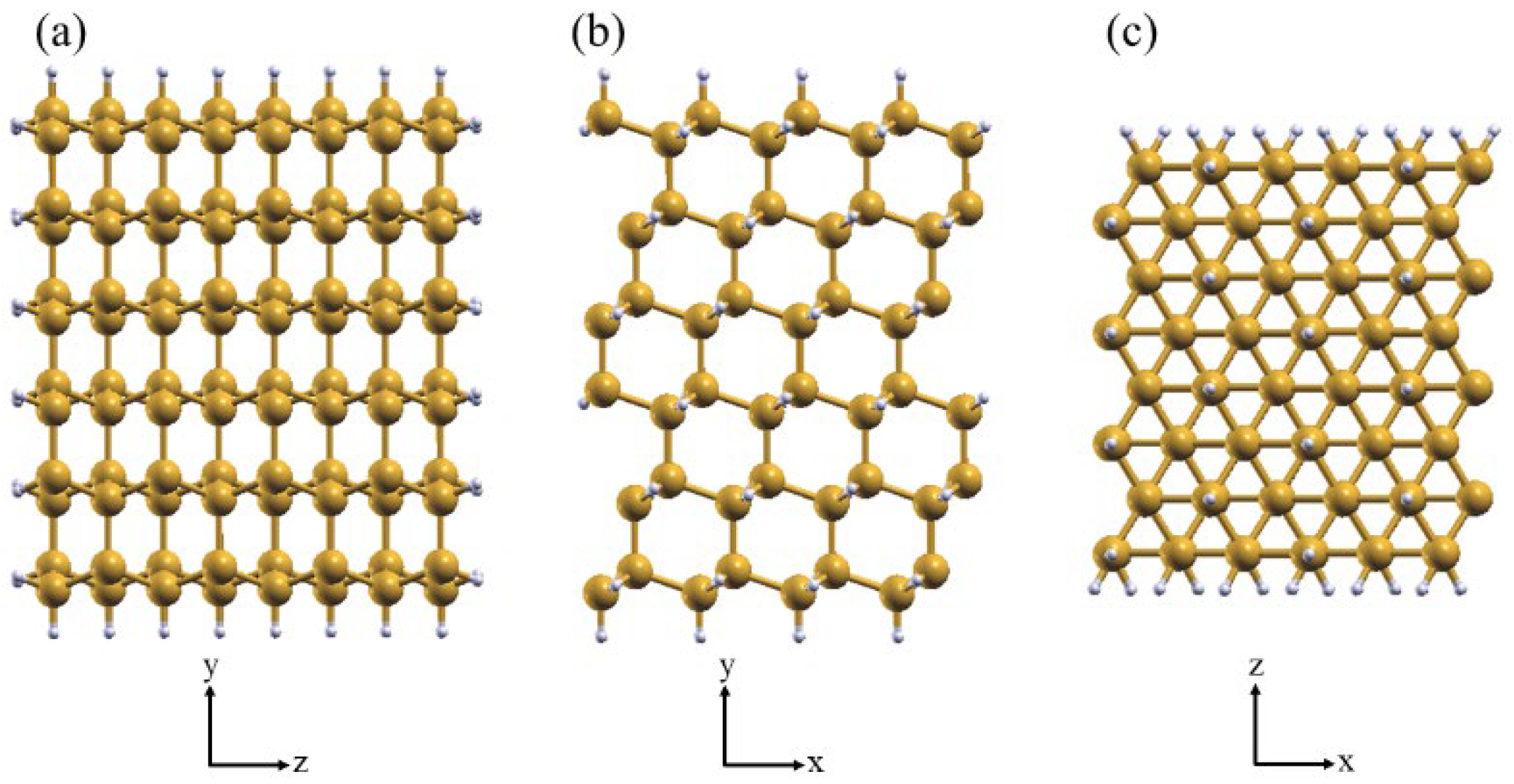
Figure 2.
Top view of the SiNW functionalized with alkyl (a,e), 1-alkenyl (b,f), and 1-alkynyl (c,g) C8 moieties grafted onto SiNW:H(111) (a-c) and SiNW:H(110) (e-f). (d) Schematic representation of the geometrical parameters used in the analysis.
Figure 2.
Top view of the SiNW functionalized with alkyl (a,e), 1-alkenyl (b,f), and 1-alkynyl (c,g) C8 moieties grafted onto SiNW:H(111) (a-c) and SiNW:H(110) (e-f). (d) Schematic representation of the geometrical parameters used in the analysis.
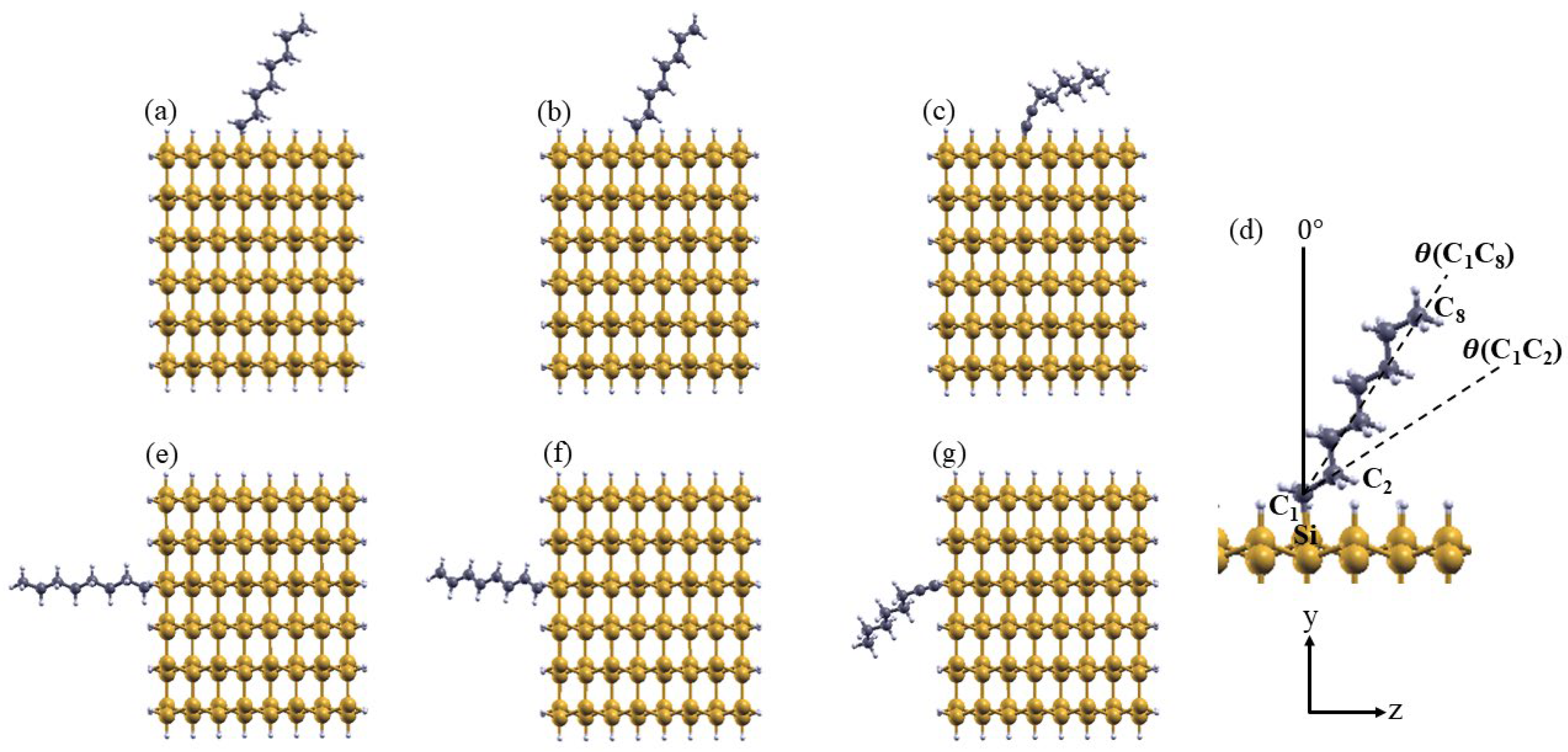
Figure 3.
Projected electron density of states (PDOS) of aliphatic C8 moieties: (a) alkyl-SiNW:H; (b) 1-alkenyl-SiNW:H; (c) 1-alkynyl-SiNW:H systems.
Figure 3.
Projected electron density of states (PDOS) of aliphatic C8 moieties: (a) alkyl-SiNW:H; (b) 1-alkenyl-SiNW:H; (c) 1-alkynyl-SiNW:H systems.
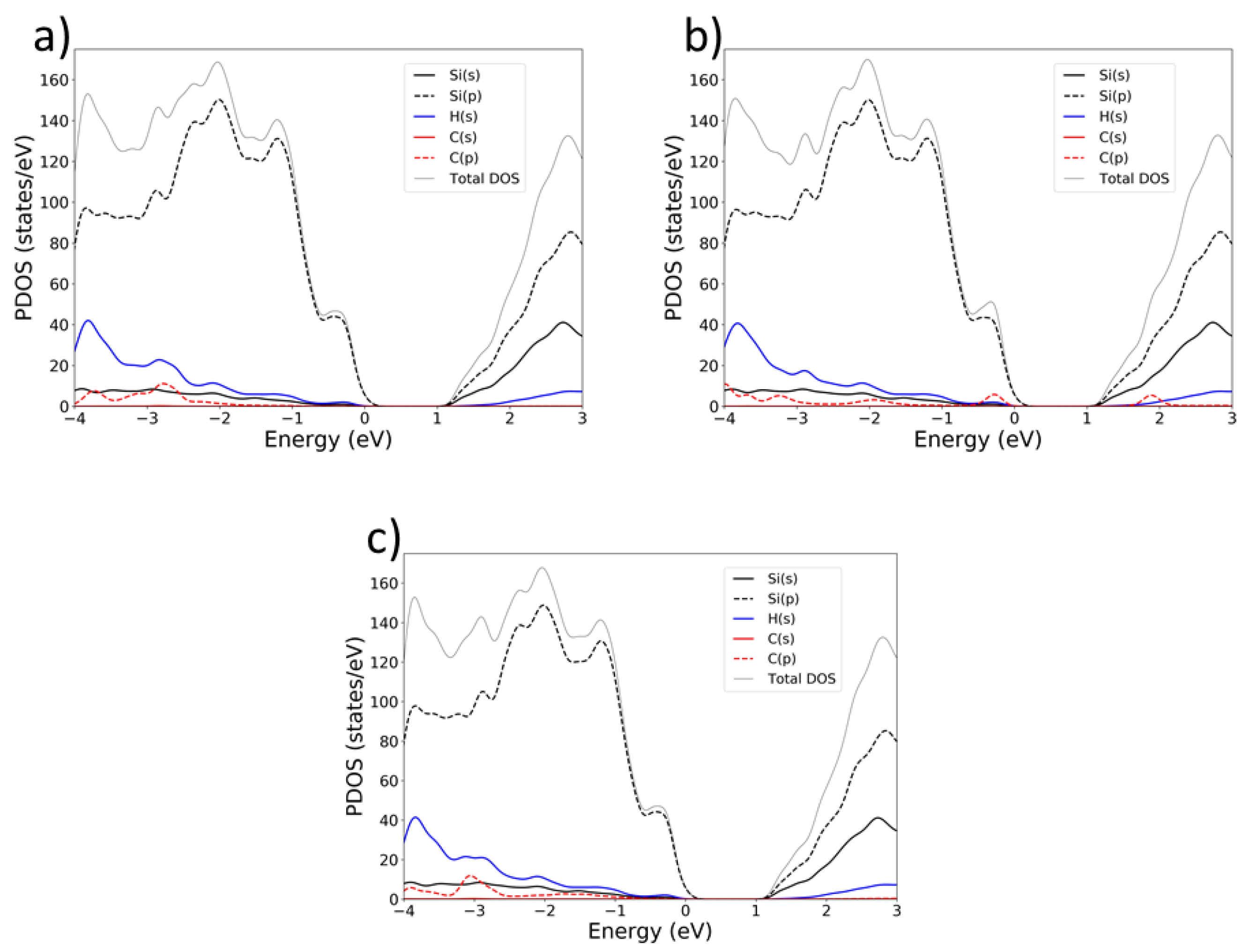
Figure 4.
Difference of the charge density of a, d) alkyl, b, e) 1-alkenyl and c, f) 1-alkynyl C8 moieties chemisorbed on SiNW:H (111) and (110) facet, respectively (yellow, white and grey spheres are Si, H and C atoms, respectively; red and blue are positive negative and negative isosurfaces, respectively; isosurface value is ±0.005 a.u.).
Figure 5.
Real part of longitudinal optical conductivity sx of alkyl-, 1-alkenyl- and 1-alkynyl-SiNW:H in the low energy range. The sx of SiNW:H is reported as reference.
Figure 5.
Real part of longitudinal optical conductivity sx of alkyl-, 1-alkenyl- and 1-alkynyl-SiNW:H in the low energy range. The sx of SiNW:H is reported as reference.
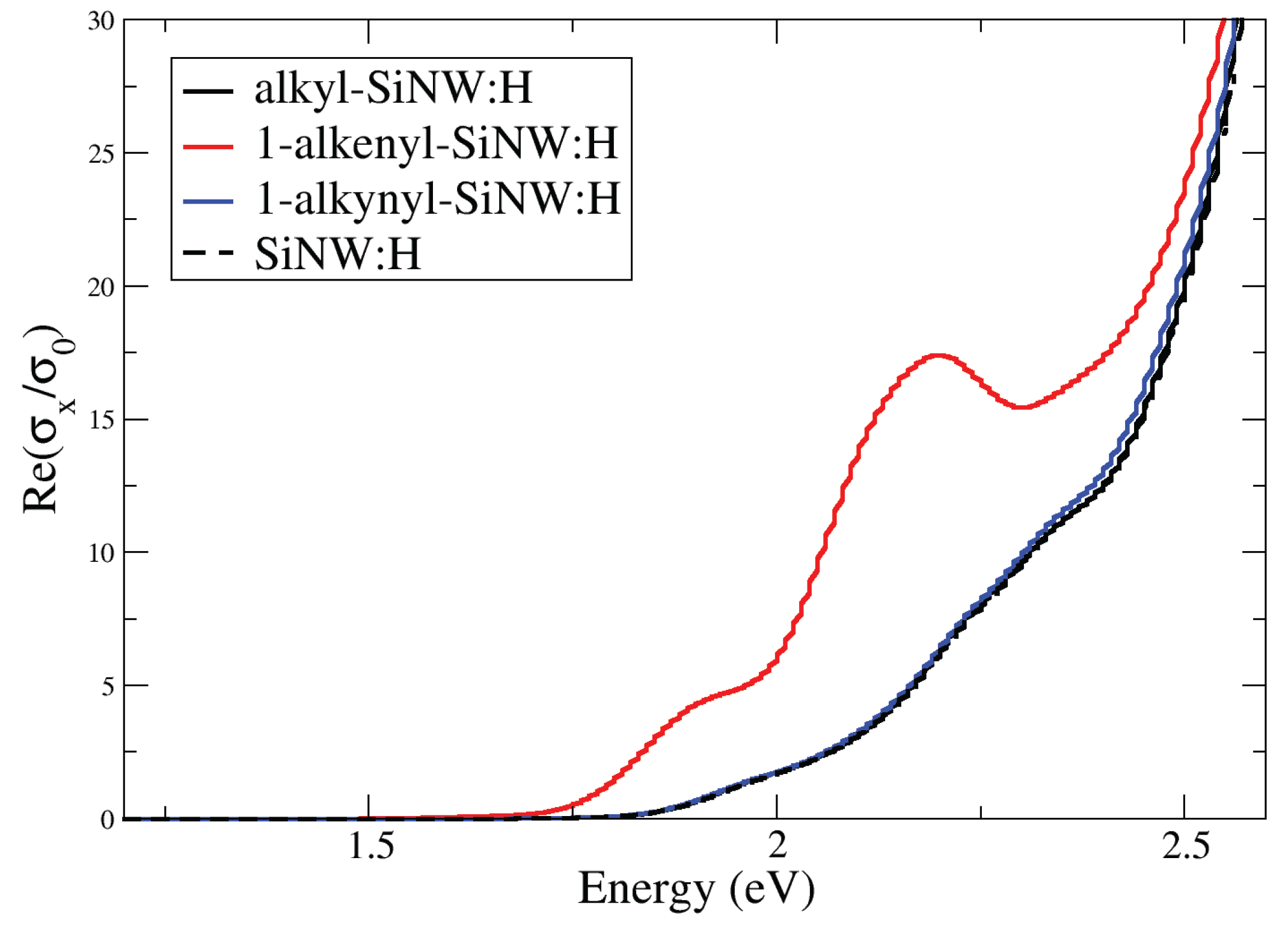

Table 1.
Geometric parameters and bond dissociation energy of the aliphatic C8 moieties chemisorbed on SiNW:H (111) and (110) facets. Refer to Figure 2 for the meaning of the listed parameters and atomic labels of the modelled systems. Bond lengths are in Ångstrom.
Table 1.
Geometric parameters and bond dissociation energy of the aliphatic C8 moieties chemisorbed on SiNW:H (111) and (110) facets. Refer to Figure 2 for the meaning of the listed parameters and atomic labels of the modelled systems. Bond lengths are in Ångstrom.
| NW Structure | θ(C1C8) | θ(C1C2) | d(C1C2) | d(C1Si) | BDE (kJ/Mol) |
| alkyl-SiNW:H (111) | 36.43 | 60.87 | 1.53 | 1.91 | 602.82 |
| 1-alkenyl-SiNW:H (111) | 35.19 | 55.13 | 1.36 | 1.87 | 712.99 |
| 1-alkynyl-SiNW:H (111) | 66.50 | 22.34 | 1.23 | 1.82 | 814.55 |
| alkyl-SiNW:H (110) | 3.54 | 32.77 | 1.53 | 1.91 | 600.08 |
| 1-alkenyl-SiNW:H (110) | 34.84 | 47.78 | 1.36 | 1.86 | 712.00 |
| 1-alkynyl-SiNW:H (110) | 56.12 | 28.55 | 1.23 | 1.82 | 820.83 |
Disclaimer/Publisher’s Note: The statements, opinions and data contained in all publications are solely those of the individual author(s) and contributor(s) and not of MDPI and/or the editor(s). MDPI and/or the editor(s) disclaim responsibility for any injury to people or property resulting from any ideas, methods, instructions or products referred to in the content. |
© 2025 by the authors. Licensee MDPI, Basel, Switzerland. This article is an open access article distributed under the terms and conditions of the Creative Commons Attribution (CC BY) license (http://creativecommons.org/licenses/by/4.0/).
Copyright: This open access article is published under a Creative Commons CC BY 4.0 license, which permit the free download, distribution, and reuse, provided that the author and preprint are cited in any reuse.


