Submitted:
28 June 2025
Posted:
01 July 2025
You are already at the latest version
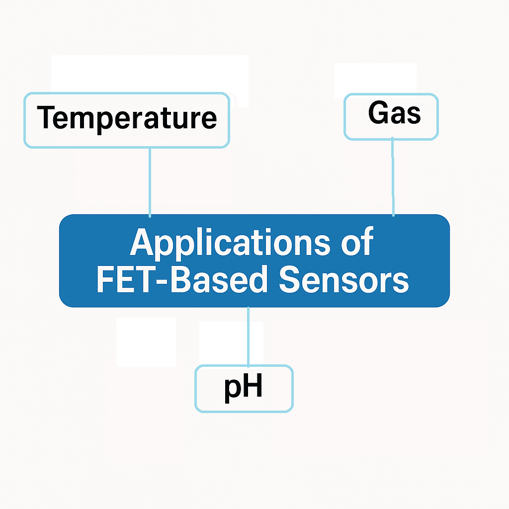
Abstract
A comprehensive update of the application of field effect transistor (FET)-based variety sensors for temperature, pH, and for gas detection is presented with a focus on the fabrication methodologies and novel materials. The introduction of modern temperature sensors based on CMOS has made a highly energy-efficient and compact design possible for integration into IoT and wearable systems. Silicon carbide (SiC) is a wide bandgap material with excellent thermal stability, suitable for high temperature and power electronics environments with compact device architectures. Due to their better chemical sensitivity on the one hand, and long-term stability and low drift on the other hand, extended gate and ion-sensitive FETs based on materials such as ZnO, RuOx, and Al₂O₃ are more suitable for biomedical and environmental monitoring in the pH sensing area. Decoupling of sensing from transistor has clear advantages of flexible design and simpler integration, as in EGFET. Sensors that made great use of the thin films of oxide metal, as well as the tunnelling-based FET structure, such as TFETs and VTFETs, have been devised to achieve high sensitivity and selectivity at ultralow voltages. In addition, the integration of simulation tools and modelling enables the conduct of more precise performance tuning and the prediction of sensor behaviour. Combined, these developments illustrate the power of FET-based sensors in formulating low-power and multipurpose sensing products for next-generation applications.
Keywords:
FETs
; Sensors
; CMOS
; SiC
; TFETs
Introduction
In the past few years semiconductor technology development and the need of smart and efficient sensing systems, have driven the evolution of the next generation sensor architectures. Of these, temperature sensors and FET based devices have become key components in several industrial sectors. They make it possible, in an accurate and real time manner, to monitor physical, chemical or biological parameters with a very high sensitivity and low power consumption. Since these are becoming more integrated into biomedical diagnostics, environmental monitoring, power electronics, and industrial systems, they are relevant in the era of miniaturized and intelligent devices.
In particular, temperature sensors have great importance for process safety and stability in high power, high performance electronic applications. An example of temperature sensors' importance is managing thermal stress in the power electronics. Temperature sensors are crucial for silicon carbide (SiC) metal oxide semiconductor field effect transistors (MOSFETs). At the same time, ultra-low power complementary metal-oxide semiconductor (CMOS) based sensors enable thermal monitoring in small and battery operated devices. However, these FET-based platforms have great potential beyond temperature sensing in biochemical and gas sensing applications. However, ion sensitive FET (ISFET), extended gate FET (EGFET) and tunnel FET (TFET) have brought new opportunities to pH detection, bio-sensing, and environmental gaseous analysis. In particular, these technologies are very useful in applications where conventional sensors cannot garner the necessary precision, scalability, or robustness [1-3].
Conventional sensor technologies, such as thermistors, resistance temperature detectors (RTD), and thermocouples, have historically been used for temperature measurements. While reliable, these sensors often present challenges in terms of integration with modern ICs, response speed, and long-term stability. CMOS based sensors addressed some of these limitations since they provided on chip integration and low power consumption[4, 5]. Further, there has been exploration of non CMOS materials such as zinc oxide (ZnO) and metal oxides (MOx) thereby leading to more sensitive sensors for gas and chemical detection. The materials innovations that support these hybrid sensing systems have allowed the realization of such systems capable of operation in harsh environments and the detection of a wide class of analytes[6, 7].
Emerging FET based sensor technologies have been introduced in order to meet the growing demands of accuracy, miniaturization and multifunctionality. One of them is advanced ISFETs with modified gate chemistries, EGFETs for modular sensing applications and TFETs for ultra sensitive detection with quantum tunnelling[8, 9]. Once developed in research laboratories, these sensors have been carrying out to practical and real-world applications which are made possible by repeated improvements in materials science, device architecture and fabrication methods. For example, ZnO and MOx EGFETs have good performance with respect to improving detection limits and selectivity for gas and biochemical species. New mixed FET designs and hybrid structures are created to locate particular sensing environments including hydrogen rich atmospheres and biologically active media[10].
FET based sensors utilize the fact that there are changes in channel conductivity realized by external stimuli like ion concentration, temperature, or presence of gases. Modifications of electric field at the gate terminal are made to control the current flow in the transistor. However, ISFETs replace the traditional gate with a membrane sensitive to the ions, and direct chemical interaction is possible[3]. On the other hand, EGFETs avoid the physical separation between the sensing element and the transistor, and the two elements can be easily maintained[8]. Low subthreshold swings very useful for low power, high sensitive applications are achieved using band to band tunneling in TFETs[1]. Despite these disadvantages, such as environmental drift, complex fabrication, low power, high response, and packaging in variable operating conditions, these technologies offer many attractive features, including low power, rapid response, and high integration potential.
The aim of this review is to give a comprehensive analysis of new and interesting temperature, gas, pH sensors, and FETs. A CMOS-compatible temperature sensor is included, and non-CMOS temperature sensors, EMI resistant and/or non-invasive, SiC-compatible sensors, and ultra-low power CMOS designs are also included in the scope. In addition, the review covers a broad range of FET-based chemical and biochemical sensors, including ISFETs, EGFETs, TFETs, and emerging hybrid architectures. It is focused on modelling strategies, simulation techniques, structural optimizations, and enhancement in material selectivity. Insights into current research trends and future directions that may help to overcome the current limitations for improving the device performance and reliability are provided.
Advanced Temperature Sensor Technologies
CMOS Technology-Based Sensors
The work presents a fully integrated, self-clocked temperature-to-digital converter-based smart temperature sensor designed for thermal monitoring of SoCs to address the self-heating problem. The design leverages the channel length modulation coefficient (λ) with MOSFET sensing, followed by a time-to-digital converter (TDC). By comparing the ratio of saturation currents of two nMOSFETs with different gate lengths but constant gate voltages, the approach enhances resolution and minimizes inaccuracies. The sensor is fabricated using a CMOS process with a compact area and employs a two-point calibration process to ensure accuracy over a broad temperature range [11]. However, MOSFET-based sensing can be limited by the effects of current gain, particularly in deep-submicron processes. To overcome these limitations, a BJT-based CMOS temperature sensor is proposed that incorporates feedback amplifier biasing of NPN transistors along with dynamic element matching (DEM). This structure effectively mitigates errors arising from the limited current gain of substrate PNP transistors. Additionally, switched capacitor (SC) integrators are implemented with single-stage cascode amplifiers for cyclic sampling and integration, simplifying the circuit design and reducing power requirements. This approach enhances current gain handling and accuracy with minimal area usage[12].
Further improvements focus on enhancing sensing accuracy and efficiency through novel architectures and compensation techniques. A temperature sensing core utilizing subthreshold current analysis is proposed, converting thermal information into frequency signals that are easily digitized. Dynamic offset compensation (DOC) is introduced to improve supply sensitivity, optimizing the sensing process while minimizing power consumption and area requirements. Systematic error removal (SER) is applied to further refine measurement accuracy, making the design suitable for on-chip dense thermal monitoring applications [13]. Additionally, a highly efficient BJT-based temperature sensor is developed using capacitively-biased PNPs driven by a regulated charge-pump. This design generates PTAT and CTAT voltages read out by an inverter-based ΣΔ ADC, achieving both energy efficiency and compactness. This approach demonstrates a significant advancement in achieving high accuracy and low power consumption, suitable for thermal management applications in sub-65nm CMOS technology [14]. In summary, continuous advancements in CMOS-based temperature sensors are effectively enhancing accuracy, energy efficiency, and compactness, making them increasingly suitable for high-performance thermal monitoring applications.
Non-CMOS Material-Based Sensors
IN a study, Er3+/Yb3+ co-doped tellurite glass (TZWLBN) was investigated for temperature sensing applications by varying the molar ratio of Yb3+ ions to determine the optimal ion concentration for the strongest luminescent emission. Using mold casting and fiber drawing techniques, a no-core tellurite fiber (NTF) was fabricated and integrated with two multimode fibers (MMFs) to form a temperature sensor. The sensor's temperature sensing characteristics were evaluated using the fluorescence intensity ratio (FIR) technique under a pumping power of 2.20 mW. Stability and repeatability were confirmed through multiple heating-cooling cycles and constant temperature tests, demonstrating practical applicability in thermal detection scenarios, particularly for monitoring the temperature of metal–oxide–semiconductor field-effect transistors (MOSFETs) [15]. To address the challenges of traditional electrical parameter-based monitoring, a non-electrical, electrically insulated temperature sensor was proposed for online condition monitoring of SiC MOSFETs in solid-state power controllers (dc-SSPC). Instead of relying on complex control systems, this method employs the case temperature as an easily measurable indicator of aging. Two characteristic parameters, meacosk and stdcosk, are introduced based on the improved cosine similarity of the case temperature waveform, effectively tracking overall aging trends and detecting severe aging in bonding wires and solder layers. The noninvasive and practical nature of this method supports fault diagnosis and predictive maintenance without disturbing the normal operation of dc-SSPCs [16].
Enhancements in temperature sensing continue to focus on improving accuracy, linearity, and energy efficiency. A low-power, high-accuracy, self-biased full CMOS temperature sensor was developed using sub-threshold currents at sub-thermal drain voltage, achieving enhanced sensitivity and linearity by generating sub-threshold current ratios with NMOS transistors of different sizes. This approach ensures stability under temperature fluctuations through a substrate diode structure, while a high-threshold comparator and timing logic control further improve accuracy and efficiency. The overall design is optimized for ultra-low power operation with high accuracy suitable for CMOS processes [17]. Additionally, a time-domain temperature sensor based on 180 nm CMOS technology introduces a diode stacking structure for improved accuracy and employs a dual-input capacitor multiplexing voltage-to-time converter (VTC) to enhance resolution. A low-temperature drift voltage-mode relaxation oscillator (ROSC) minimizes the impact of temperature-induced delay errors, ensuring high-resolution sensing. This combination of enhanced accuracy, low power consumption, and high resolution makes this design suitable for modern applications demanding precise temperature monitoring [18].In conclusion, the development of advanced temperature sensors utilizing innovative architectures and techniques such as FIR technique, non-electrical monitoring, sub-threshold current analysis, and time-domain sensing significantly improves accuracy, efficiency, and reliability, making them suitable for various high-performance thermal monitoring applications. Figure 1
Temperature Sensors for SiC MOSFETs
Characterization of a temperature sensor based on a diode connected 4H-Silicon Carbide (4H- SiC) p-type metal oxide semiconductor field-effect transistor (MOSFET) is performed over wide temperature range. The study shows that the sensor primarily depends on the characteristics of the threshold voltage but at temperatures below 76K, the arising device current begins to act nonlinearly as it shows an unusual decrease. As such, researcher define two distinct temperature ranges at which the sensor operates, one at 76K to 175K with high linearity and moderate sensitivity, and the other above 175K, where the sensitivity is higher at the cost of slightly reduced linearity. Additionally, the device is compatible with 4H-SiC CMOS technology and thus useful for inclusion into integrated circuits where it can be applied for high temperature applications [19]. Nevertheless, SiC MOSFETs suffer from the problem of gate oxide degradation, especially at high temperatures. This is addressed by proposing a method for the temperature independent monitoring of gate oxide degradation. The approach has the effect of reducing temperature sensitivity through the measurement of the minimum turn off circuit parasitic inductor voltage (vcir_min) under certain conditions. High temperature gate bias (HTGB) experiments and double pulse tests are used to validate this technique by proofing the robustness against temperature fluctuations as well as other variables such as bus voltage, load current and bond wire failure [20].
A novel online method of temperature measurement and monitoring is utilized that embeds the linear relation between drain–source current (Ids) and the power MOSFET temperature to achieve further improvement in temperature measurement and monitoring. A technique that can accurately detect temperature under real working conditions is realized by superimposing a pulse on the gate and measuring the resulting instantaneous current. The proposed design also includes the circuitry to counter the effect of electrical bias change and maintain stability and reliability during temperature measurement. The practicality of the approach is verified by means of infrared thermal imaging [21]. Moreover, a novel MOS gate power device junction temperature monitoring sensor is introduced by making use of a temperature sensitive resistor built from the polycide gate electrode layer. Here, researchers use this method, which requires no additional fabrication steps, to effectively isolate the resistor from current and voltage transients and therefore in-situ monitor the junction temperature during active circuit operation. For instance, its implementation in Silicon Carbide Junction Barrier Schottky Field Effect Transistors (SiC JBSFETs) proves it to be practical for real-time temperature monitoring in harsh environments [22].
General Temperature Sensors for Power Devices
Key to power MOSFET reliability and health management is accurate online junction temperature (Tj) extraction. But currently most temperature-sensitive electrical parameters (TSEPs) in SiC power MOSFETs have low temperature sensitivity that precludes high accuracy and requires high bandwidth measurement circuits. As a remedy for this, Linear-Mode Current Response (LMCR) method is proposed as a high sensitive Tj extraction method. A theoretical formula for drain current in linear mode is established and verified using simulations and experiments. Demonstrating high sensitivity (with minimal additional losses), independent of load current and bus voltage, the method uses a narrow current pulse for the linear mode response and finds Tj from the pulse response. The approach is experimentally validated on a SiC power boost converter [23]. An inverse heat conduction problem (IHCP) framework is developed to estimate heat sources and internal temperature distribution while addressing the external measurements' limitations in integrated module. The framework uses a sequential time domain method coupled with Tikhonov regularization to predict the heat sources from limited, noisy data at an enhanced computational efficiency through a finite element model reduction exploiting Krylov subspace. It has been shown to be practical, by achieving synchronization to various sensor systems that would provide critical information on otherwise unmeasured heat sources and temperature contours. To verify the efficiency and accuracy of the framework, it is experimentally validated with a BLDC motor drive module [24].
Moreover, measurements of mechanical stress wave of PSDs are made to study effect of temperature on ‘PSDs.’ The traditional approach to performing this purpose has been Acoustic Emission Testing (AET), yet its use is hindered by temperature effects. However, to overcome this limitation, non contact laser Doppler vibrometry (LDV) is introduced, which provides enhanced capability to detect temperature dependent turn off stress wave variations. By reflecting temperature dependent characteristics effectively, this technique broadens the scope of condition monitoring of PSDs particularly in SiC MOSFETs [25]. It is also important to improve thermal impedance measurement (Zth) and power cycle testing (PCT) of the semiconductor power packages for accurate junction temperature measurement. Existing static temperature calibration methods lead to significant errors when the virtual junction temperature (Tvj) in an advanced SiC MOSFET is evaluated. To account for the transient effects that arise when performing Zth and PCT analysis under switched gate bias conditions, a new dynamic calibration method was proposed to improve the accuracy of the measurements. A comprehensive comparison of SiC MOSFETs from many manufacturers is conducted to validate that this method is robust for accurate junction temperature measurement and lifetime characterization [26]. The proposed methods are proven to effectively improve the accuracy, efficiency, and reliability of temperature measurement for semiconductor applications of different kinds by employing novel sensing techniques and calibration methods.
EMI-Resistant and Non-invasive Temperature Measurement
Analog sensor inaccuracy due to external Electromagnetic Interference (EMI) signals can lead to a loss on security and reliability of a sensor system. In order to solve this problem, a self check method introduced to automatically detect and fix EMI disturbed measurements by a dummy sensing element that is only sensitive to EMI noise. It works by switching between the two modes using switching devices and therefore is able to characterize EMI signals in the normal mode using the computed response in the self check mode. EMI responses between both modes are made consistent by considering key factors that are the properties of the dummy sensing element, operational amplifier input voltage, and power supply rails. This is a completely cost effective approach to fault localization because it is using minimal additional components and computational resources [27]. Yet, improving the efficiency in thermal monitoring for power electronic systems as applied to electric vehicle (EV) traction inverters featuring silicon carbide (SiC) MOSFETs has been a challenge.
A high efficiency, sensorless estimation technique with dual gate bias (DGB) was introduced as a method to improve thermal monitoring in silicon carbide (SiC) MOSFETs, where third quadrant characteristics of the MOSFETs are utilized. It dynamically builds a temperature function through the combination of mosfet operating currents and bus voltage and current, decoupling the motor effect with two stage current pulse accurately estimating temperature. This method is unlike traditional methods because it does not need additional circuits, therefore it is highly cost effective and may be integrated into existing systems [28]. A thermal simulation model is developed using FLUENT software for the analysis of temperature rise characteristics of MOSFETs with varying void rates on printed circuit board for addressing overheating issues in automotive electronic water pumps. It has been concluded that thermal resistance increases with increasing void fraction and single voids present lower thermal resistance than multi voids if the void ratio is higher than 10%. Results from this model lead to insight regarding improvement in the dissipation of heat and reduction in MOSFET thermal failure in harsh automotive operating environments [29]. An on chip temperature sensor with dynamic slope compensation (DSC) is proposed as an accurate temperature sensor for high performance processing chips. To make use of the subthreshold current ratio of two subthreshold MOSFETs in a proportional conversion to duty cycle while able to preserve linearity in the face of process variations. This method is implemented with the low area and power consumption, greatly improving the supply sensitivity and measurement accuracy by eliminating the systematic errors and trimming one point, suitable for the dense thermal monitoring applications [30].They have improved the sensor accuracy, improved the thermal monitoring efficiency and avoided the EMI sources. Figure 2
Low-Power & Nano-Watt CMOS Temperature Sensors
In this work, we discuss different ways to improve the performance of temperature sensors in terms of power efficiency, compactness, and accuracy. A nano-watt digital output temperature sensor is introduced, which uses a supply insensitive self-biased current source to achieve a stable reference and a linear temperature sensitive voltage, where second order temperature dependencies of the MOS diode are effectively cancelled. Integrating a sensing unit, voltage controlled differential ring oscillators, and low power frequency to digital converter with a resistor less design, this architecture minimizes power and area. A delay element in the ring oscillator reduces stage count and improves noise performance and compactness. The sensor is fabricated in 65 nm CMOS, occupying 0.02 mm 2, and consumes 60 nW, making it a viable choice for low power applications [31]. A fully digital temperature sensor based on the temperature characteristics of MOSFET leakage current was proposed to further optimize energy efficiency and accuracy. Temperature to frequency conversion is achieved using a Leakage Dominated inverting Schmitt Trigger (LDST) and a ring oscillator. An Adaptive Resolution Frequency-to-Digital Converter (AR-FDC) is designed in this work to enable these features, faster measurement speed at high temperatures to prevent chip overheating, and high resolution at lower temperatures. The fabricated sensor, using a 55 nm CMOS process, consumes low power and offers higher resolution, which is suitable for on chip thermal management systems [32].Figure 3
Another proposed sensor circuit embeds a 12-bit SAR ADC with a 1 bit temperature-voltage (T V) comparator in an attempt to improve temperature voltage sensitivity and energy efficiency. The design improves temperature voltage sensitivity by implementing a novel load capacitor imbalance technique and enhances system energy efficiency without the use of off chip voltage references. Furthermore, an on chip PTAT voltage source provides additional sensitivity refinement to make the sensor highly efficient at low power operation. Compared to previous methods, this sensor shows over 50% improvement in temperature voltage sensitivity and can be applied to energy efficient systems [33]. In addition to these sensor design advances, thermal through silicon using (TTSV) technology is investigated to mitigate mismatch of the coefficient of thermal expansion of the Si substrate and filler metal, thereby alleviating thermal stress. Finite element analysis and temperature dependent simulations indicate that the TTSV diameter and its distance from the MOSFET can affect electron mobility, hole mobility, saturation current and threshold voltage. This study highlights the importance of optimizing TTSV dimensions and positioning for mitigating thermal stress effect, so as to improve device performance and reliability at ultra low temperature [34].In summary, these novel approaches can improve temperature sensor performance through power efficiency, accuracy improvement, and also the management of thermal stress effect, which are suitable for advanced thermal monitoring applications. Figure 4

Table 1.
Table 1.Comparison of Advanced Temperature Sensors.
| SENSOR TYPE | TEMPERATURE RANGE | LINEARITY | SENSITIVITY | ADDITIONAL FEATURES | REFERENCE |
|---|---|---|---|---|---|
| Diode-connected 4H-SiC p-type MOSFET | 14K - 482K | 0.991 (76K - 175K), 0.986 (>175K) | 6.24mK/K (3.34nA), 66.37mV/K (263nA) | 4H-SiC CMOS compatible, Unusual reduction in current below 76K | [19] |
| SiC MOSFETs in EVs | Not Specified | N/A | 7.2% estimation error | Sensorless thermal monitoring, No hardware changes required, Utilizes dual-gate bias (DGB) strategy | [28] |
| MOSFET in Automotive Water Pumps | Not Specified | N/A | Thermal resistance increases with void fraction | Single void more effective at >10% void ratio, FLUENT software simulation | [29] |
| Digital Temperature Sensor (55nm CMOS) | -10°C - 120°C | N/A | Resolution FoM: 208 pJ⋅K2, 112 mK resolution | Adaptive Resolution FDC, 7.2 μW power consumption, Ultra-small sensing front-end | [32] |
| Nano-watt Digital Output Temperature Sensor (65nm CMOS) | -20°C - 120°C | N/A | Resolution: 0.2°C (rms), Resolution FoM: 0.022 nJ·K−2 | 60 nW power consumption, 0.02 mm² area, Suitable for wireless sensing systems | [31] |
| LMCR-based Tj Extraction (SiC Power Boost Converter) | Not Specified | N/A | High Tj sensitivity, Low interference | Non-invasive, High measurement sensitivity, Effective at eliminating high-bandwidth circuit requirements | [23] |
| EMI-Resistant Sensor Measurement | Not Specified | N/A | Enhances measurement accuracy under EMI | Cost-effective, Low demand for additional components, Effective EMI correction | [27] |
| Low-power CMOS Temperature Sensor (28nm CMOS) | Not Specified | N/A | 0.98-mV/K T-V sensitivity, 0.15K resolution | 12.6 pJ per conversion, 0.29-pJ ⋅ K2 FoM, On-chip PTAT voltage source | [33] |
| IHCP Framework (Sensor Systems - Thermocouples) | N/A | Good linearity with computational efficiency | Effective estimation of heat sources and temperature contour | 200 W BLDC motor drive module for collaborative robots | [24] |
| SiC MOSFET Gate-Oxide Degradation Monitor | 25–150 °C | Temperature-independent | 6.55% and 0.103% changes in vcir_min | Effective in temperature fluctuation scenarios | [20] |
| TTSV (Thermal Stress Analysis) | 173–573 K | Dependent on TTSV diameter and distance | Impact on electron mobility, saturation current, and threshold voltage | Applicable to NMOS transistors with TTSV | [34] |
| SiC MOSFETs Online Temperature Measurement | N/A | Good linearity between Ids and temperature | Validated via infrared thermal imaging | Power MOSFETs under actual working conditions | [21] |
| Junction Temperature Monitoring Sensor | N/A | Linear relationship during operation | Enables in-situ monitoring | SiC JBSFETs with BiDFET | [22] |
| Noncontact LDV (Stress Wave Measurement) | N/A | Effective temperature-dependent stress wave measurement | Reflects temperature-dependent variations | Condition monitoring of PSDs | [25] |
| On-Chip Temperature Sensor | -20°C to 120°C | Proportional operation ensuring linearity | Inaccuracy of +1.2/-1.0°C (3σ) after calibration | High-performance processing chips | [30] |
| Dynamic Calibration for Zth and PCT | N/A | Transient response-based calibration | Improves Tvj measurement accuracy | Lifetime characterization of SiC MOSFETs |
[26] |
| Self-Clocked Temperature-to-Digital Converter | −40°C to 100°C | High | 0.036°C | Two-point calibration, Area: 0.047 mm² | [11] |
| BJT-based CMOS Temperature Sensor | −40°C to 120°C | High | ±0.97°C | Single-point calibration, Area: 0.075 mm² | [12] |
| Er3+/Yb3+ Co-doped Tellurite Glass Temperature Sensor | 253 K to 443 K | Moderate | 0.00264 K−1 | Repeatability & Stability Tested, Max Error: 0.88 K | [15] |
| Non-Electrical SiC MOSFET Temperature Sensor | N/A | N/A | N/A | Noninvasive Online Monitoring | [16] |
| Subthreshold Current-Based CMOS Temperature Sensor | −40°C to 120°C | High | 2.1 °C/V | Two-point calibration & SER, Area: 860 μm² | [13] |
| Sub-1V BJT-based Temperature Sensor | −40°C to 125°C | High | 0.41 pJ.K² | One-point trim, Area: 0.01 mm² | [14] |
| Self-Biased Full CMOS Temperature Sensor | −10°C to 100°C | High | 40 mK | Two-point calibration, Ultra-low power: 11 nW | [17] |
| Time-Domain Temperature Sensor | 0°C to 120°C | High | 0.0071°C | Low power: 1.48 μW, High resolution | [18] |
| High-Accuracy Temperature Sensor | -55 to 150 °C | ±0.4 °C (3σ) | Resolution: 0.0156 °C (14-bit ADC) | Asymmetric operational amplifier, Extended counting ADC, 0.18-μm CMOS process | [35] |
| 4H-SiC High Temperature CMOS Technology | Above 500 °C | Not specified | Blocking Voltage: Over 700 V | Lateral power transistors, UV photodiodes, High-temperature metallization layers | [5] |
| Energy-Efficient CMOS Temperature Sensor | -40°C to 125°C | +0.71/−0.73°C | Resolution: 0.17°C, Energy: 96.7 pJ | Low-power design, On-chip oscillator, Operating Voltage: 0.5 V, Area: 0.025 mm² | [4] |
FET-Based Sensors for pH Sensing Applications
High-Sensitivity TFET & Advanced ISFETs
In order to improve pH biosensor performance, we use this study to explore the improvement in sensitivity, accuracy and speed of the biosensor using advanced device architecture and materials. In particular, the biomolecule diffusion within the nanocavity (Tbio) region of a split gate, step channel electrolyte insulated semiconductor vertical TFET (SGSC-EIS-VTFET) pH biosensor was investigated first. Improved drain current (Ids), transconductance (gm), current sensitivity (SID) and voltage sensitivity (SV) (up to SV = 145 mV pH−1, exceeding the Nernstian limit (59.2 mV pH−1), and simultaneously tenfold increase in SID per pH variation were performed by physics modeling, however the sensing mechanism, as well as the analyte conjugation, mainly limited performance [1]. In order to avoid this problem, a Hetero JuncEtion Extended Source Electrode Vertical TFET (HJ ESVTFET) is proposed based on electrode and cavity length extension in a SiGe p+ pocket doped Si / Gi vertical TFET. To this end, band narrowing, sensitivity and sensing speed were improved by two orders of magnitude for neutral biomolecules and three orders of magnitude for charged biomolecules (k = 5) with a 6 times increase in sensitivity of band conduction over conventional V-TFETs and a 50% reduction in transit time, [2]. The limitations of silicon based technology were overcome by comparing the performances of Ion Sensitive Field Effect Transistors (ISFETs) with SiC (6H-SiC) technology and it was found that SiC (6H-SiC) technology had superior performance to the same technology in silicon. Key metrics, including threshold voltage (Vth), drain saturation current (IDsat), transconductance (gm), and ION/IOFF ratio, exhibited linear variation with pH, with SiC ISFETs demonstrating higher sensitivity: Vth (60 mV/pH), IDsat (8 μA/pH), gm (7 μS/pH), and ION/IOFF ratio (7.6 × 10⁶/pH), proving SiC technology to be highly promising for pH sensing applications [3].The study demonstrates that novel architectures like HJ-ESE-VTFET and advanced materials like SiC significantly enhance pH biosensor sensitivity, speed, and performance, making them promising for high-performance pH sensing applications.
Practical EGFET Sensors for Real-World Applications
A study examines a variety of material and configuration choices that can improve the performance, stability, and practicality of Extended-Gate Field-Effect Transistor (EGFET) sensors used to detect samples for any number of applications, such as environmental monitoring, agricultural sensing, and medical diagnostics. The performance and stability of EGFET pH sensors using conventional external Ag/AgCl, external Au and integrated Au reference electrodes was compared to determine optimal configuration. Compared to the individual electrodes, the integrated Au electrode provided superior stability and comparable sensitivity (96 mV/pH with 97% linearity from pH 4 to 10) along with the least drift and therefore is a promising alternative for realizing practical, portable EGFET pH sensor. Upon this, a precision agriculture EGFET soil pH sensor based on a low cost, all solid state EGFET utilizing a planar Ag/AgCl reference electrode (PARE) consisting of titanium nitride (TiN) was developed. I etched a TiN pH electrode, which had a high sensitivity of 57.25 mV/pH and improved hydrophilicity (water contact angle of 46.425º). The use of oxalic acid post-conditioning on the sensor proved to be both reliable for measuring soil pH with small error and reusable, making for good long term use in agricultural monitoring [8]. A potassium ion sensor of EGFET configuration using Ag/AgCl based pseudo reference electrodes (PRE) and gold solid contact electrodes (SCE) on a small PCB substrate provided further improved cost effectiveness, sensitivity and stability. Overall, this sensor displayed a level of stability (<1 mV/day drift), sensitivity (49 mV log[K+]), and rapid response (<10 secs) while it was showing good and reliable performance over the whole pH range (4 to 10). It exhibited good current sensitivity (1.43 (μA)1/2 /log [K+]) and is a practical solution for nutrient monitoring in precision agriculture [9]. Moreover, a DI-pretreated RuOx based EGFET sensor was additionally developed to overcome the sub Nernstian sensitivity limitation and achieved a super Nernstian pH response of 64.13mV/pH with 0.997 linearity by enhanced hydration which increases the reactive surface sites for proton adsorption and desorption. The DI pretreated RuOx sensor demonstrated low hysteresis (< 2 mV), little drift (0.25 mV/h), high repeatability (97.95% retention) and long term stability (120 days), which showed its potential to become a high performance pH sensor [10]. Together, these findings demonstrate the progress of EGFET sensors from new electrode configurations, materials selection and optimization techniques that address previous limitations and enable the sensor to function with further increased sensitivity and stability as well as better practical usability for many applications.
ZnO/MOx-Based EGFET Materials Study
It is a complete evaluation of different materials and structures in Extended Gate Field Effect Transistor (EGFET) based pH sensors for further improvement of sensitivity, stability, and functionality in practical applications. In a study, Liquid phase exfoliation of PP was performed for the creation of a phosphorene (PP) modified zinc oxide (ZnO) EGFET pH sensing system with spin coating of the PP onto FTO glass. It had the potential to sense the accuracy in biomedical pH monitoring with a sensitivity of 62.5 mV/ pH, linearity of 0.993, a hysteresis voltage of 10 mV, and drift rate of 0.714 mV/h [36]. To a broader comparative study, metal oxide (MOx) thin films of TiO₂, ZnO, CuO and NiO were used as EGFET pH sensing electrodes by using a sol-gel spin coating technique. With the aspect of sensitivity, the lowest hysteresis (1 mV) and best sensitivity of 53.4 mV/pH, showing better surface morphology by means of FESEM and AFM, (15) showed the best wear durability stability. Also, sensing films of ZnGa₂O₄ were prepared by RF magnetron sputtering and connected to commercial MOSFETs. Therefore, fabrication of oxygen sensors with sensitivities up to 23.14 mV/pH and current sensitivity of 33.49 μA/pH and with good linearity up to 96.15% are demonstrate strong functions of fabrication conditions [37]. Moreover, hydrothermal and sputtering based synthesis of TiO₂ and Pt/TiO₂ nanorods on FTO substrate was found to improve the performance. Bare TiO₂ was superior due to increase in its surface reactivity, conductivity, and surface roughness compared to Pt/TiO₂, which gave 50 mV/pH and 63.8 μA/pH voltage and current sensitivity, respectively, and is very suitable for biomedical applications [38]. A novel double gate ZnO thin film ISFET was first introduced, which omits the need of a reference electrode by using capacitive coupling of top and bottom gates. The performance of an EGFET based pH sensor exceeds the Nernst limit with high linearities (R2 values of 0.984 and 0.964) [39], and this device achieved exceptional voltage sensitivity of 205.57 mV/pH and current sensitivity of 10.82 mA/mm·pH, a drastic improvement over previous report [40].
ISFET Variants & Modelling Approaches
A comprehensive study to improve the sensitivity, stability and efficiency of Ion Sensitive Field Effect Transistors (ISFETs) for application in pH sensing with different materials, architectures, and operational approaches are presented in the study. Initially, the gate electrode work function of ISFETs was analyzed using the Cogenda Visual TCAD tool, revealing that molybdenum, with a work function of 4.75 eV, exhibited superior performance over aluminum, providing higher threshold voltage, switching ratio (10⁴), and lower leakage current (10⁻³) at 300 K. Experimental validation demonstrated instability in ISFETs manifested as drift in threshold voltage over time, particularly when tested at increasing pH levels of 4.67, 5.9, 7.5, 8.57, and 9.3 [41]. For more sensitivity, the 2D oxides in 2D channel material ISFETs were then theoretically studied, comparing 2D-3D oxide stacks versus purely 3D oxide based ISFETs. The 2D-3D oxide stack showed a higher current sensitivity (36.36 nA/pH) and better transconductance to drain current ratio sensitivity (0.338 V¹pH⁻¹), as compared to 3D oxide based ISFET and can be used as a next generation pH sensor [42]. Reduced Graphene Oxide (rGO) was also investigated as a possible substitute for the conventional Metal Oxide because of its higher sensitivity and lower threshold voltage. COMSOL Multiphysics software was used for multiphysics modeling to confirm that rGO performs better than the commercial products, and rGO has the potential to be employed in the development of more efficient and reliable pH sensing devices for various scientific and industrial applications [43]. Additionally, out-of equilibrium body potential (VB) in silicon-on-insulator (SOI) double gate ISFET like devices was used as a novel pH detection method. Super Nernstain sensitivity with lower power consumption was achieved by the sensor through the pH dependent modulation of the conductive channel at Si/BOX interface and using VB as a read method. The TCAD simulations also suggested that improved sensitivity could be achieved through alteration of the architecture, and thereby VB monitoring was identified as a very attractive approach in terms of low power and high performance for pH sensing [44].Overall this study shows that material, architecture and sensing method optimization can greatly enhance ISFET performance in making efficient, low power sensitive pH sensors.
Emerging FET Architectures & Hybrid Concepts
We investigate in this study novel ways of overcoming limitation in pH sensor performance using innovative designs, materials and architectures. To better understand the sensing mechanism of a pH sensor based on pEFT, an electrochemical equivalent circuit for an extended gate field effect transistor (EGFET) pH sensor was first designed and simulated using LTSpice XVII. Finally, the simulation proved that the capacitors attached to the MOSFET gate were most critical to the drain current (ID), while the resistors were not, as ionic exchange determines sensor behavior. But this approach only shows sensing mechanism simulated but it does not help with sensitivity and reliability [8]. To improve sensitivity to pH, a vertically grown GaSb/InGaAs hetero junction negative capacitance vertical tunnel FET (Hetero-NC-VeTFET) sensor with ferroelectric materials used for inducing negative capacitance effect were developed to address this. In this design, efficient tunneling at the source/channel junctions with GaSb and InGaAs gave rise to order of 10⁵ improvements in drain current voltage and transconductance sensitivity. Despite that, the fabrication limitations and the lack of structural alignment still had an impact on the performance [45]. In order to eliminate these fabrication challenges, a double gate Electrolyte Insulated Semiconductor (ES-VTFET) pH sensor was proposed, focusing on the negative impact of vertical gate misalignment in short channel structures. To make the device more suitable for real world applications, this device was modified to be a pH sensitive material by modeling the electrolyte region as an intrinsic semiconductor with well defined dielectric properties [46]. Such improvements, however, did not overcome the challenge of material selection for reaching high sensitivity and reliability. In order to further extend the dynamic range and improve performance, a copper gallium oxide (CGO)-based extended gate field effect transistor (EGFET) pH sensor was developed that uses amorphous CGO thin films deposited by co-sputtering of Cu and Ga₂O₃ targets. This sensor exhibited excellent linearity with a voltage sensitivity of 51 mV/pH, current sensitivity of 80 μA1/2/pH, and a net hysteresis value of approximately 0.003 V, demonstrating superior stability and reliability across a broad pH range of 2 to 10, making it a promising candidate for high-performance pH sensing [47].This study demonstrates that combining improved architectures, materials, and modeling techniques effectively enhances pH sensor sensitivity, reliability, and practical applicability.
Mixed-FET Designs with Specialized Targets
By using novel materials, architectures and readout schemes, the study makes a progressive improvement in the sensing of pH using the current configurations. First, a novel potentiometric readout circuit for pH sensing in oral healthcare devices based on Correlated Double Sampler topology developed along with a switched-capacitor based low pass filter (SC-LPF) to reduce power consumption, area and common CMOS amplifier limitations. An implementation of this integrated circuit with 0.18 µm CMOS process was implemented and showed excellent noise (0.683 µVrms) and power (124.1 µW) characteristics, suitable for in vivo use [48]. Despite this design, they did not alleviate the sensitivity limitations of conventional pH sensor. An ISFET model with a silicon base and Al₂O₃ oxide layer was developed to improve sensitivity and its sensitivity is found to be 58.97 mV/pH. This design also defined optimal criteria for oxide thickness and channel length, thus a reliable framework for ISFET model design for medical, food, and environmental monitoring [49]. However, conventional oxide materials still remain limited in their sensitivity. This problem was addressed through a vertical nanowire feedback field effect transistor (VNFISFBFET) with Al₂O₃-SiO₂ as a sensitive layer. This design achieved up to a 5.53 factor ION/IOFF ratio, with better current sensitivity (3927) and voltage sensitivity (2.73) and especially useful for work functions of >4.3 eV. It has sufficient sensitivity and operates under low power conditions such that it is a promising candidate to replace traditional oxide based sensors [50]. In addition, another study developed a dual source T channel TFET (DST-TFET)-based pH sensor that can achieve even higher sensitivity at ultra low power as its SV is about five fold above the Nernst limit of 59 mV/pH, and it reaches 297.66 mV/pH at 0.1 V operating voltage. However, in ultra low power environment the device showed good performance and enhanced IDS–VGS characteristics at lesser sensitivity, and sensitivity decreased with temperature [51]. Collectively, these advancements describe collectively a systematic evolution towards development of high performance and low power pH sensors for a wide range of biomedical, environmental and industrial applications.Figure 5.
Simulation, Mapping & Specialized Bio-Sensors
Gradually increasing the sensitivity, compatibility, and scalability of field effect transistor (FET) based pH sensors, a study addresses the limitations of sensitivity, compatibility, and scalability in terms of the novel materials, designs, and modelling. To begin with, it developed a surface-potential (SP) based compact model for 2D material based pH sensitive FETs using Poisson’s equation, site binding theory and Gouy–Chapman–Stern approach for handling electrostatics of the electrolyte side and 2D density states and Fermi–Dirac statistics for the electrostatics of the channel side. The performance of this model was validated using experimental data from ISFETs based on TMD materials and was high accuracy and compatible with SPICE circuit simulations making it a promising choice for practical pH sense [52]. Despite metallic properties and weak field effect, commonly used materials like Laser-Induced Graphene (LIG) make it difficult to reach high performance FET based sensors. In order to address that, LIG electrodes fabricated by laser scribing on polyimide (PI) were proposed as a cost effective, disposable, and high surface area sensing electrodes for FET based chemical sensors. Using this approach, the sensitivity reached 30.9 mV/pH for pH sensing or −46.9 mV/dec for sodium ion sensing, depending on the membranes used, while being compatible with all of those materials mentioned above including PI adhesive tape, PI insulated Ag wire, and PI based FPCBs [53]. Although LIG electrodes bring obvious advantages with high fidelity, real time and high resolution pH signals are difficult to achieve. In order to overcome this, FET based biosensors (bio-FETs) have been developed with high sensitivity, low temperature dependence and scalability for use in high spatial resolution pH sensing. Recently there has been the development of static arrays with directly wired sensor pixels and active matrix arrays requiring additional switching FETs thus allowing these arrays to be applied to biomedical fields such as health monitoring, DNA sequencing, and elongation [54]. These advancements together reflect fundamental progress in improving on pH sensor performance by harnessing accurate modeling, novel electrode materials, and manufacture of pH sensors array, which create the foundations for future systems capable of next generation, high resolution pH sensing. Table .2
Table 2.
Comparison of pH Sensor Technologies.
| Sensor Type | Description | Material/Technology | Sensitivity/Noise | Linearity | Additional Characteristics | Reference |
|---|---|---|---|---|---|---|
| Potentiometric Readout Circuit | pH-sensing system in oral healthcare device | 0.18 µm CMOS process | 0.683 µVrms | ±1.5 V | 5 pF load, 1 MHz input clock | [48] |
| Hetero-NC-VeTFET Sensor | Vertically grown GaSb/InGaAs hetero-junction NC sensor | GaSb and InGaAs | Not specified | Not specified | Sensitivity in the order of 105 | [45] |
| PP-Modified ZnO EGFET Sensor | EGFET pH sensor with PP-modified ZnO | FTO glass | Sensitivity: 62.5 mV/pH | 0.993 linearity | Hysteresis: 10 mV, Drift Rate: 0.714 mV/h | [36] |
| EGFET with Integrated Au Electrode | EGFET pH sensor with integrated Au electrode | Integrated Au Electrode | 96 mV/pH sensitivity | 97% linearity | pH range: 4 to 10, Improved stability | [55] |
| ISFET Sensor (Analog Study) | Theoretical and experimental study of ISFET for pH sensing | Molybdenum, Aluminum | Sensitivity: pH range: 4.67 - 9.3 | Not specified | Threshold voltage, Switching ratio (104), Leakage current (10⁻³) | [41] |
| ISFET with Si/Al2O3 Membrane | ISFET pH sensor using Si base and Al2O3 oxide layer | Si, Al2O3 | Sensitivity: 58.97 mV/pH | Not specified | Application: Medical, Food, Water Monitoring | [49] |
| 2D-3D Oxide ISFET | 2D oxide & 3D oxide-based ISFET for pH sensing | 2D oxide, 3D oxide | 36.36 nA/pH (Current Sensitivity) | Not specified | Transconductance ratio sensitivity: 0.338 V/pH⁻¹ | [42] |
| EGFET with Electrochemical Circuit | EGFET pH sensor simulated using electrochemical circuits | MOSFET, Resistors, Capacitors | Not specified | Not specified | LTSpice Simulation, Electrochemical Mechanism | [7] |
| ES-VTFET Sensor | Bio-TFET-based pH sensor using electrolyte dielectric | Electrolyte (dielectric constant: 78) | Not specified | Not specified | Drain current, Transconductance, Voltage sensitivity | [46] |
| ISFBFET | Ion sensor using Al2O3-SiO2 sensitive layer | Al2O3-SiO2 | ION/IOFF = 10¹⁰, Sensitivity: 3927 (Current), 2.73 (Voltage) | Not specified | Low power, High sensitivity, Steep response | [50] |
| DST-TFET | Dual-Source T-channel TFET-based pH sensor | SiO2, HfO2, Al2O3 | Sensitivity: 297.66 mV/pH | Not specified | Ultralow operating voltage (0.1 V) | [51] |
| TiN-PARE Soil pH Sensor | Low-cost EGFET soil pH sensor with TiN sensing film | TiN, Ag/AgCl | Sensitivity: 57.25 mV/pH | >0.99 linearity | Soil pH, Hydrophilicity, Reusability | [8] |
| SP-Based 2D Material FET | SP-based compact model for 2D-material ISFETs | TMD materials, Verilog-A | Not specified | Not specified | SPICE-Circuit Simulation, Heterostructure ISFETs | [52] |
| rGO ISFET Sensor | Comparison of rGO and Metal Oxide gate layers for pH sensing | rGO, Metal Oxides | Enhanced sensitivity, Lower threshold voltage | Not specified | Improved performance for pH monitoring | [43] |
| MOx EGFET Sensor | Comparative study of MOx materials (TiO2, ZnO, CuO, NiO) | MOx Thin Films |
Sensitivity: 53.4 mV/pH | R² = 0.992 | Hysteresis: 1 mV, Drift Rates (pH 10, 7, 4) | [56] |
| ZnGa2O4 EGFET Sensor | ZnGa2O4 sensing films for EGFET pH sensing | ZnGa2O4 | Sensitivity: 23.14 mV/pH, 33.49 μA/pH | 92.1% - 96.15% | Annealing process analysis, Oxygen flow rate adjustment | [37] |
| RuOx EGFET Sensor | DI-pretreated RuOx-based EGFET sensor | RuOx | Sensitivity: 64.13 mV/pH | 0.997 | Low hysteresis (~2 mV), Drift rate (0.25 mV/h), Long-term stability | [10] |
| SGSC-EIS-VTFET | Step-channel EIS-VTFET for biosensing | Vertical TFET, Si, Oxide | Sensitivity: 145 mH/pH | Not specified | Enhanced SID, Diffusion mechanism, Biomolecule detection | [1] |
| CGO EGFET Sensor | CGO-based EGFET for pH sensing | Cu-Ga2O3 | Sensitivity: 51 mV/pH | 99.59% | Current sensitivity: 80 μA¹/²/pH, Low hysteresis | [47] |
| HJ-ESE-VTFET | SiGe p+ Pocket doped Si/Ge vertical TFET | SiGe, Ge, Extended Source | 5.5x higher sensitivity | Not specified | Improved speed, Enhanced sensing capabilities | [2] |
| LIG-FET Sensor | LIG-based FET for pH and sodium sensing | LIG on PI, MOSFET | 30.9 mV/pH (pH), -46.9 mV/dec (Na+) | Not specified | Flexible, Disposable, Low-cost sensing electrodes | [53] |
| Bio-FET Arrays | pH mapping using bio-FET sensor arrays | Bio-FET arrays | High sensitivity | Not specified | Static & Active-matrix arrays for biomedical applications | [54] |
| SiC ISFET | SiC (6H-SiC) vs Si-based ISFETs for pH sensing | Si, 6H-SiC | 56 mV/pH (Si), 60 mV/pH (SiC) | Not specified | Better performance of SiC ISFET over Si ISFET | [3] |
| DG-ZnO ISFET | Double-gate ZnO thin-film ISFET for pH sensing | ZnO | 205.57 mV/pH (Voltage), 10.82 mA/mm.pH (Current) | 0.984 (Voltage), 0.964 (Current) | High-performance, Reference-free operation | [39] |
Advances in FET Gas Sensors
Evolving Sensing Materials & Selectivity
For growth of high sensitivity and low power gas sensor, we solely focused the exploration of advanced materials for growing layered zinc indium tin oxide (ZITO) films deposited by co-sputtering.In a study, Indium tin divinylsulfide films have been grown by researchers who controlled the material properties by changing the ratio of ZnO to ITO, they were able to obtain both strong sensing behaviors at higher temperatures for oxygen vacancy rich films, as well as lower temperatures for hydroxy rich films. These results indicate that one can tailor the material composition such that good gas response and good power per unit gas response can be achieved [6]. Although such sensors are promising in terms of gas responsivity, their thermal stability in addition to comprehensive performance optimization in many cases, is still lacking in many studies. To address this, structural integrity as well as noise were improved and the detection limit lowered (from 1.8 ppb to 0.29 ppb) and oxygen vacancies were reduced [57]. While these advances in sensitivity and stability still not good enough for conventional metal oxide sensors to detect in payload specification hazardous gases, such as nitrous oxide (NO₂) and sulfur oxide (SO₂). A novel TT-Pc electron rich structure was used in organic field effect transistor (OFET) sensors, over coming that, which have the capability of performing selective detection of NO₂ and SO₂ with a high sensitivity and environmental stability [58]. Although this is a sustainable and selective solution, it is challenging to adapt such organic devices to continue to scale in next generation semiconductor platforms. A conducting polymer (CP) gate all around junctionless transistor (GAA-JLT) gas sensor proposed and simulated was used to bridge this gap. In the environmental conditions different from CpHAC, performance can be optimized as work function of CpHAC depends on gas interactions and the quality of doping. A such hybrid scheme can offer high sensitivity, selectivity, and adaptive features to the next generation of semiconductor technologies and was proved to be a promising future for the next generation of reliable and efficient gas sensors [59].It shows advancements in gas sensor technology, with improved sensitivity and selectivity among different materials.
Enhancing Device Architecture for Hydrogen Sensing
A novel hydrogen (H₂) gas sensor is described using a vertically extended gate field effect transistor (VEG-FET) based on LUT modeling and simulation. Therefore, by increasing the area over which H₂ molecules are adsorbed onto a Pt Parylene-C channel that is vertically extended from a given area, more than ten times sensitivity is achieved by increasing drain current (IDS) from 150.7 mA to 310.3 mA at 0.5 torr [60]. It serves to integrate modeling and readout circuitry, but it does not completely solve the issue of comparing various catalytic materials to further increase sensitivity. To overcome this problem reserchers use a Junctionless Gas Tube FET (JL GT FET) model with Pt and Palladium (Pd) as catalytic gates, the metal work function modulation is an important mechanism for H2 detection. The JL-GT-FET have superior pressure sensing performance than Nanowire FETs by analytically modeling, simulating and 3D device simulator coherence [61]. However, the sensitivity is still not very high and complex doping processes have to be tolerated. To conquer this, another model is developed as p-type MoTe₂ MOSFET incorporating charge plasma electrodes and Pd hydrogen sensing region to sense without MoTe₂ doping. From Non- equilibrium Green’s Function (NEGF) simulations, predictions are made on carrier transport and sensing capabilities of p-type FET [62]. In turn, this means that there are still limits to the performance possible under variable conditions. Consequently, the resolution of this problem is using the architectures of catalytic metal gate (CMG)-based nanosheet FET (NSFET) and nanosheet tunnel FET (NSTFET) in ultra-scaled devices. Optimal gate stack and bandgap engineering was performed to withstand doping and bias variations giving a 650 % sensitivity improvement across the range of H₂ pressure. Thus, the optimization benchmarking shows that the CMG N.STFET is the most performing and reliable sensor under low pressure H₂ environment compared to other nanostructured CMG.FET and TFET based sensors [63]. It concludes with the agreement of the adsorption efficiency, metal work-function modulation and removal of the requirement for doping for hydrogen sensing as clear progression for hydrogen sensing technologies.
Structural and Thermal Optimization for Broader Reliability
The work introduces for the first time catalytic based metal gate charge plasma (CP) MOSFET for enhancing the sensitivity in gas detection. TCAD simulations verify construction of CP-MOSFETs having source and drain regions without traditional doping using metals having the appropriate work functions such as palladium (Pd) for hydrogen and silver (Ag) for oxygen, on a piece of intrinsic silicon [64]. The CP MOSFET structure is however effective for dealing with fabrication complexity, but it still inherits most of the traditional silicon which may restrict its electric performance. To tackle this issue, a FinFET with dual gate dielectric stack and a gallium arsenide (GaAs) channel is proposed for O₂ sensing. Analysis of the gate sensitivity to work function shift on O₂ exposure shows the same increase in sensitivity, and when compared with conventional silicon FinFETs this GaAs based FinFET outperforms them in ION, IOFF and subthreshold swing (SS). It goes on to perform parametric analysis of fin with width, gate length and dielectric material on its sensing behavior [65]. However, gas sensors are not reliable in thermal terms. To address this, a field effect polymer transistor type gas sensor platform is developed with embedded poly silicon micro heater that accounts for thermal efficiency as well as long term reliability. COMSOL simulations of the thermal response offer improved heat distribution, while mild power consumption increase of 1.22x is sufficient to improve lifetime by over 14 times with just an asymmetrical air gap design, and technologies on winding manufacture [66]. Nevertheless, the sensing performance becomes inconsistent in the presence of structural variability found in the next generation transistor architectures such as GAA FET's. This is overcome by an analytical model of a gate all around junctionless transistor (GAA-JLT) with elliptical cross section using nonuniform oxide thickness. Sensitivity metrics are evaluated under geometric variations, and results also show that the device geometry and the operating conditions can be tuned to increase hydrogen sensing accuracy and device robustness, something which confirms the robustness of the variability aware design [67].The technological evolution in materials, architectures and in the thermal design has resulted in truly robust gas sensors characterized by great sensitivities.
Advanced TFET Architectures and Multigas Capability
Ammonia gas sensors are important due to the danger of a toxic exposure to ammonia. To overcome the challenging requirement of having the efficient detection method with sensitivity up to 55% enhancement, a novel ammonia gas sensor based on the Multi Wall Carbon Nanofibers (MWCNFs) as the active sensing material on the field effect transistor (FET) platform are developed [68]. However, conventional FET sensors still usually do not meet the ideal low power performance and gas selectivity. To address this, a heterogeneous source lateral n-type tunnel FET (DSHS nTFET) based on stacked source is conceptually proposed to exploit the stacked source in both increasing electron tunneling efficiency and sensitivity. In the range of 200 K to 400 K, catalytic metals of Pt, Co, Pd, and Ag is used to sense NH₃, CO, H₂, and O₂ for work function modulation with high Ion/Ioff ratios, and near unchanged performance [69]. Although these advantages exist, there is still a need for the miniaturization and ability to detect multiple gases. To satisfy this, a phosphine (PH₃) sensitive Stack Engineered Junctionless Accumulation Nanowire FET (SE-JAM-NW FET) with low power consumption, nanoscale features and high sensitivity is introduced with the use of catalytic metals (Pt, Rh, Ir, Pd). Sensitivity is quantified in terms of variations of current and channel geometry, and there is a strong correlation between the analytical and simulation results [70]. On the other hand, SE-JAM-NW FET is a compact and tunable device, but further improves the sensitivity for ammonia detection in TFET designs. Hence, shape engineered and source engineered TFETs such as SiGe pocket based DG TFET, vertical TFET, Z shape and U shape configurations are manufactured. It is further found that the best performing U-shape TFET is the one obtained by optimal tuning of the molybdenum gate work function between 4.40–4.60 eV , which leads to Ion = 8.01 × 10⁻⁴ A/μm and high Ion/Ioff ratio of 1.25 × 10¹³[71]. As a result, the SiGe pocket U shape TFET moves the focus from sensitivity to current efficiency and represents the highest performing ammonia sensor and provides mitigations to the power and selectivity challenges of conventional FET ammonia sensors.
Conclusions
In summary, this review highlights growing importance of temperature and FET-based sensors technologies in biomedical diagnostics, environmental monitoring, power electronics and the quickly growing field. With state of the art CMOS and non CMOS temperature sensors, ISFETs, EGFETs, TFETs and the hybrid FET designs there has been very significant advantages over traditional sensing methods, i.e., higher sensitivity, lower power consumption and better integration potential. Continuous efforts to improve performance, energy efficiency and adaptability to harsh environments have been ongoing, which means that the developments reflect key improvements such as temperature sensors fine-tuned to use with SiC MOSFETs, EMI-resistant designs, or nano-watt CMOS implementations. Another point of the review is that ZnO/MOx materials provide superior selectivity, stability, and their role in modeling and simulation as a mean for optimising ISFET behavior. While all of these advances had been made, lasting reliability, calibration in the real world, and scalable fabrication technology remained empty. Much recent research is devoted to structural and thermal optimization, as well as to new FET architectures and hybrid materials for hydrogen sensing. Facing new concepts and new materials, integration of “traditional” technologies is already opening interesting vision of creating robust, multifunctional, and intelligent sensor platforms. Towards the end of the day though, it is challenging to elevate the field to a level of maturity where more general types of sensing will emerge, and the trajectory toward innovation ultimately suggests highly capable, miniaturized sensors that will define the future of sensing in many different domains.
Declarations
Acknowledgments
The authors would like to express sincere gratitude to the Shreenivas Deshpande Library at the Indian Institute of Technology (BHU) Varanasi for providing invaluable resources and support.
Author Contributions
DUR: Written original draft; conducted a survey of the literature; prepared the tables; collected the references; methodology; edited the final manuscript. All authors have approved the final version of the manuscript.
Funding
No funding was provided for the development of this manuscript.
Availability of data and material
All data relevant to this review are included in the text, references, tables, and figures.
Ethics approval and consent to participate
Not applicable.
Consent for publication
Not applicable.
Conflicts of Interest
The authors declare that they have no competing interests.
References
- Wadhwa, G., et al., Performance analysis based on biomolecule position and pH-sensing mechanism for vertical TFET. Physica Scripta, 2024. 100(1): p. 015029. [CrossRef]
- Singh, J. and S. Singh, Improvement in the sensing performance of SiGe pocket Si/Ge VTFET based biosensor using extended source electrode and nano-cavity length. Materials Science and Engineering: B, 2024. 310: p. 117688. [CrossRef]
- Hebali, M., et al., Enhancement of pH-Sensor Sensitivity Using Si and SiC ISFETs Transistors. Silicon, 2023. 15(12): p. 5245-5251. [CrossRef]
- Jayaram, C. and P. Sreehari, An Energy-Efficient Fully On-Chip CMOS Temperature Sensor for Portable Applications With an RFoM of 2.79 pJ. K2. International Journal of Circuit Theory and Applications, 2024.
- May, A., et al. A 4H-SiC CMOS technology enabling smart sensor integration and circuit operation above 500 C. in 2024 Smart Systems Integration Conference and Exhibition (SSI). 2024. IEEE.
- Shin, H., et al., Optimization of co-sputtered zinc indium tin oxide-based MOSFET-type sensor for effective NO2 gas detection. Sensors and Actuators B: Chemical, 2025. 428: p. 137262. [CrossRef]
- Hashim, S.B., et al. Understanding the Extended-gate FET pH Sensor Sensing Mechanism through Equivalent Circuit Simulation in LTSpice. in 2024 IEEE International Conference on Automatic Control and Intelligent Systems (I2CACIS). 2024. IEEE.
- Mamilla, S., et al., A Low-Cost, Reusable All-Solid-State TiN-Based EGFET Soil pH Sensor. IEEE Sensors Journal, 2024. [CrossRef]
- Abhinav, V. and T.R. Naik, Low-Cost, Point-of-Care Potassium Ion Sensing Electrode in EGFET Configuration for Ultra-High Sensitivity. IEEE Access, 2024.
- Singh, K., et al., Enhancing pH Sensing Capabilities through Hydroxylated Surface Groups on RuO x Flexible EGFET Sensor. IEEE Sensors Journal, 2024.
- Chakraborty, K. and A.J. Mondal, On-chip oscillator based temperature-to-digital converter exploiting channel length modulation coefficient λ. Integration, 2024. 96: p. 102168.
- Lai, X., et al., A 0.075 mm2 BJT-based temperature sensor with a one-point trimmed 3σ inaccuracy of±0.97° C from− 40° C to 120° C. Microelectronics Journal, 2024. 153: p. 106418.
- Zhang, T., et al., A Compact Temperature to Frequency Converter With 3σ Inaccuracy of+ 0.57° C/-0.65° C for On-Chip Thermal Monitoring. IEEE Sensors Journal, 2024. 24(7): p. 9427-9436.
- Tang, Z., et al. A 0.8 V Capacitively-Biased BJT-Based Temperature Sensor with an Inaccuracy of±0.4° C ($\mathbf {3}\mathbf {\sigma} $) from− 40° C to 125° C in 22nm CMOS. in 2024 IEEE Symposium on VLSI Technology and Circuits (VLSI Technology and Circuits). 2024. IEEE.
- Wu, Y., et al., A Low Pumping Power Excited Er 3+/Yb 3+ Co-Doped Tellurite Temperature Sensor for Thermal Monitoring of MOSFET in Complex Circuits. IEEE Sensors Journal, 2024. 24(7): p. 10098-10104.
- Yu, B., et al., Case Temperature Waveform Similarity-based Online Aging Monitoring for SiC MOSFETs of Accelerated Power Cycling Tests for DC-SSPCs. IEEE Journal of Emerging and Selected Topics in Power Electronics, 2024.
- Lei, B. and Y. Zeng, An 11 nW,+ 0.34° C/− 0.38° C inaccuracy self-biased CMOS temperature sensor at sub-thermal drain voltage. AEU-International Journal of Electronics and Communications, 2024. 187: p. 155554.
- Sun, Y., et al., A Sub-0.01° C Resolution All-CMOS Temperature Sensor with 0.43° C/− 0.38° C Inaccuracy and 1.9 pJ· K2 Resolution FoM for IoT Applications. Micromachines, 2024. 15(9): p. 1132.
- Rinaldi, N., et al., Analysis of a 4H-SiC lateral PMOSFET temperature sensor between 14K-482K. IEEE Sensors Letters, 2025.
- Zhou, X., et al., A Temperature-Independent Gate-Oxide Degradation Monitoring Method for Silicon Carbide Metal Oxide–Semiconductor Field-Effect Transistors Based on Turn-Off Ringing. Electronics, 2025. 14(4): p. 771.
- Meng, X., et al., Online temperature measurement method for SiC MOSFET device based on gate pulse. IEEE Transactions on Power Electronics, 2024. 39(4): p. 4714-4724. [CrossRef]
- Narwal, R., et al. FET junction temperature monitoring using novel on-chip solution. in 2024 IEEE Applied Power Electronics Conference and Exposition (APEC). 2024. IEEE.
- Yang, F., et al., A High-Sensitive Online T j Extracting Method Based on Electrothermal Interaction and Linear-Mode Current Response for Power MOSFET Devices. IEEE Transactions on Power Electronics, 2025.
- Lee, J.-w., et al., Heat source and internal temperature estimation of an integrated modular motor drive in robotic application using inverse heat conduction problem. Measurement, 2025. 243: p. 116297. [CrossRef]
- Ping, Y., et al., Analysis of the Influence of Temperature on Turn-off Stress Waves in SiC MOSFET Using Laser Doppler Vibrometry. IEEE Sensors Journal, 2024.
- Breuer, J., et al. Challenges of Junction Temperature Calibration of SiC MOSFETs for Power Cycling–a Dynamic Approach. in CIPS 2024; 13th International Conference on Integrated Power Electronics Systems. 2024. VDE.
- Jia, Z., et al., A Self-Check Method for Enhancing the Measurement Accuracy of Analog Sensors under Electromagnetic Interference. IEEE Transactions on Instrumentation and Measurement, 2025. [CrossRef]
- Lu, Y., et al., Sensorless Junction Temperature Estimation of Onboard SiC MOSFETs Using Dual-Gate-Bias-Triggered Third-Quadrant Characteristics. Sensors, 2025. 25(2): p. 571.
- Lyu, S., et al., Analysis on thermal simulation of MOSFET based on voids under working conditions. Microelectronics Reliability, 2025. 165: p. 115585.
- Zhang, T., et al., A 700nW Compact Temperature Sensor With a One-Point Trimmed Inaccuracy of+ 1.2/–1.0∘ C For On-Chip Thermal Monitoring. IEEE Transactions on Circuits and Systems II: Express Briefs, 2024.
- Naveed and J. Dix, An Ultra-Low-Power 0.8 V, 60 nW Temperature Sensor for Battery-Less Wireless Sensor Networks. Journal of Low Power Electronics and Applications, 2025. 15(1): p. 1.
- Yang, Z., H. Li, and P. Zhang, A fully digital temperature sensor with 187-μ m 2 front-end for on-chip thermal management in 55-nm CMOS. Analog Integrated Circuits and Signal Processing, 2025. 122(2): p. 21. [CrossRef]
- Tang, J. and X. Tang, A 12.6-pJ/Conversion Temperature Sensor With 0.98-mV/K Temperature-Voltage Sensitivity. IEEE Transactions on Circuits and Systems II: Express Briefs, 2025.
- Xie, W., et al., The Effect of Through-Silicon-Via Thermal Stress on Metal-Oxide-Semiconductor Field-Effect Transistor Properties Under Cooling to Ultra-Low Temperatures. Micromachines, 2025. 16(2): p. 221. [CrossRef]
- Wang, Y., et al., A fully integrated temperature sensor with an inaccuracy of±0.4° C (3σ) from− 55 to 150° C. Microelectronics Journal, 2024. 154: p. 106463.
- Lai, C.-H., et al., Phosphorene Modified Zinc Oxide for Extended-Gate Field-Effect Transistor pH Sensors. IEEE Sensors Journal, 2025.
- Chen, C.-H., S.-B. Liu, and S.-P. Chang, Performance improvement of a ZnGa2O4 extended-gate field-effect transistor pH sensor. ACS omega, 2024. 9(13): p. 15304-15310.
- Huang, C.-S., et al., Enhanced pH Sensing Capability by Platinum Adsorption onto Titanium Dioxide Nanorods. IEEE Sensors Journal, 2024. [CrossRef]
- Srikanya, D., A.M. Bhat, and C. Sahu, Design and analysis of high-performance double-gate ZnO nano-structured thin-film ISFET for pH sensing applications. Microelectronics Journal, 2023. 137: p. 105811.
- Kamarozaman, N.S., et al., Sensitivity Study of Spin-Coated Metal Oxides Thin Films for Extended Gate Field-Effect Transistor (EGFET) pH Sensor. Transactions on Electrical and Electronic Materials, 2024. 25(4): p. 411-421. [CrossRef]
- Pathak, Y., et al., Experimental circuit design and TCAD analysis of ion sensitive field effect transistor (ISFET) for pH sensing. Materials Science and Engineering: B, 2024. 299: p. 116951.
- Sarath, S., et al. Exploring pH Sensing in MoS 2-Based ISFETs with 2D-3D Gate Oxide Stacks. in 2024 IEEE SENSORS. 2024. IEEE.
- Estakhroyeh, H.R., M. Mehran, and E. Rashedi. Enhanced Sensitivity of ISFET pH-Sensor Utilizing Reduced Graphene Oxide. in 2024 6th Iranian International Conference on Microelectronics (IICM). 2024. IEEE.
- Alepidis, M., et al., Super-Nernstian pH detection using out-of-equilibrium body potential in silicon on insulator ISFET sensors: Proof-of-concept and optimization paths. Sensors and Actuators A: Physical, 2024. 373: p. 115439. [CrossRef]
- Bera, P.K., et al., Detection sensitivity analysis of a vertical TFET biosensor using a negative capacitance GaSb/InGaAs electrolyte pH sensing system. Ionics, 2025: p. 1-11.
- Khan, M.H., et al., Evaluation of sensitivity in a vertically misaligned double-gate electrolyte-insulator-semiconductor extended source tunnel FET as pH sensor. Micro and Nanostructures, 2024. 196: p. 208005. [CrossRef]
- Dai, Y.-E., et al., Amorphous Copper Gallium Oxide Extended Gate Field-Effect Transistor PH Sensor. IEEE Sensors Journal, 2024.
- Lakshminarayana, S., et al., A CMOS Switched Capacitor Filter Based Potentiometric Readout Circuit for pH Sensing System. Journal of Low Power Electronics and Applications, 2025. 15(1): p. 3.
- Jhankar, S.P., et al. Improvement of Voltage Sensitivity of pH Sensor Based on Ion Sensitive Field Effect Transistor. in 2024 IEEE International Conference on Power, Electrical, Electronics and Industrial Applications (PEEIACON). 2024. IEEE.
- Kumar, P., et al., Low-Voltage Feedback Field Effect Transistor based Ion-Sensing: A Novel and Detailed Investigation for energy-efficient pH Sensor. IEEE Sensors Letters, 2024.
- Yousf, N., et al., Ultralow-Power DST-TFET pH Sensor Exceeding the Nernst Limit with Influence of Temperature on Sensitivity. ACS Applied Bio Materials, 2024. 7(7): p. 4562-4572.
- Nazeer, T. and S. Aamir Ahsan, Analyzing Few-Layer and Heterostructure pH-Sensitive 2D-Material Field-Effect Transistors Using a Physics-Based SPICE Compact Model. ACS Applied Electronic Materials, 2024. 6(7): p. 5085-5093.
- Na, Y.J., et al., Laser-Induced Graphene as Versatile Sensing Electrodes for Extended-Gate Field-Effect Transistors. IEEE Sensors Journal, 2024. [CrossRef]
- Ren, H., et al., Field-effect transistor-based biosensor for pH sensing and mapping. Advanced Sensor Research, 2023. 2(8): p. 2200098.
- Yeh, J.-T., et al., Comparison between Different Configurations of Reference Electrodes for an Extended-Gate Field-Effect Transistor pH Sensor. ACS Omega, 2025.
- Zainal, N., et al. Electrochemical EGFET pH Sensing Performance using ZnO-based Composite Thin Films Sensing Electrode. in 2023 IEEE Regional Symposium on Micro and Nanoelectronics (RSM). 2023. IEEE.
- Shin, W., et al., Does a large response suffice?: Thermally stable and low noise Si-doped IZO thin-film transistor-type gas sensors. Sensors and Actuators B: Chemical, 2025. 422: p. 136498.
- Isci, R., et al., Highly sensitive OFET based room temperature operated gas sensors using a thieno [3, 2-b] thiophene extended phthalocyanine semiconductor. Journal of Materials Chemistry C, 2025. 13(1): p. 472-483.
- Sharma, P. and P. Kumar, Sensitivity analysis of methanol, chloroform, and dichloromethane using GAA-JLT-based gas sensor. Micro and Nanostructures, 2024. 195: p. 207947. [CrossRef]
- Martha, P., et al., Design and analysis of a vertically extended gate field effect transistor (VEG-FET)-based hydrogen gas sensor: a comprehensive modeling and simulation approach. Journal of Materials Chemistry C, 2025.
- Goel, A., S. Rewari, and R. Gupta, Performance investigation of neoteric Pt/Pd Junctionless gas tube FET (JL-GT-FET) as a Hydrogen (H2) gas sensor for industrial applications-analytical model. Micro and Nanostructures, 2025. 198: p. 208050.
- Kanrar, S.S. and S.K. Sarkar, Non-equilibrium Green's function analysis of charge plasma-based source-drain electrode P-type MoTe2 MOSFET for high sensitivity hydrogen sensing. Micro and Nanostructures, 2024. 189: p. 207823.
- Bansal, G., et al., Catalytic Metal-Gated Nano-Sheet Field Effect Transistor and Nano-Sheet Tunnel Field Effect Transistor Based Hydrogen Gas Sensor-A Design Perspective. Advanced Theory and Simulations, 2024. 7(3): p. 2301031.
- Dewangan, N., et al., A highly sensitive MOSFET gas sensor based on charge plasma and catalytic metal gate. International Journal of Numerical Modelling: Electronic Networks, Devices and Fields, 2024. 37(2): p. e3191.
- Kumari, A. and R. Das, Sensitivity analysis on stack gate-dielectric GaAs tri gate FinFET based oxygen gas sensor. Applied Physics A, 2024. 130(6): p. 422. [CrossRef]
- Park, J., et al., Reliability of FET-type gas sensor with asymmetric air-gap micro-heater structure considering thermoelectric effect. Sensors and Actuators B: Chemical, 2024. 405: p. 135349.
- Sharma, P., S. Kumar, and P. Kumar, Proposal for variability-induced effective radius of elliptical gate-all-around junctionless transistors and its applicability in hydrogen gas sensors. AEU-International Journal of Electronics and Communications, 2024. 180: p. 155337.
- Shooshtari, M., Ammonia gas sensors based on multi-wall carbon nanofiber field effect transistors by using gate modulation. Colloids and Surfaces A: Physicochemical and Engineering Aspects, 2025. 704: p. 135563.
- Mili, G., Z. Liana, and B. Bhowmick, Sensitivity Analysis of a Double Source Stack Lateral TFET-Based Gas Sensor. ECS Journal of Solid State Science and Technology, 2024. 13(2): p. 027001. [CrossRef]
- Sharma, S., et al., Modeling and Simulation Characteristics of a Highly-Sensitive Stack-Engineered Junctionless Accumulation Nanowire FET for PH3 Gas Detector. ECS Journal of Solid State Science and Technology, 2024. 13(2): p. 027007.
- Hirphaa, Y.G., et al., Impact of SiGe pocket on different shape TFET structures for gas sensing application. Micro and Nanostructures, 2024. 196: p. 207998. [CrossRef]
Figure 1.
CMOS temperature sensor architecture (A) Temperature sensing core with reference generation and CTAT/PTAT outputs. (B) Voltage-to-time conversion timing. (C) Temperature-to-digital conversion using relaxation oscillator and counter [18].
Figure 1.
CMOS temperature sensor architecture (A) Temperature sensing core with reference generation and CTAT/PTAT outputs. (B) Voltage-to-time conversion timing. (C) Temperature-to-digital conversion using relaxation oscillator and counter [18].
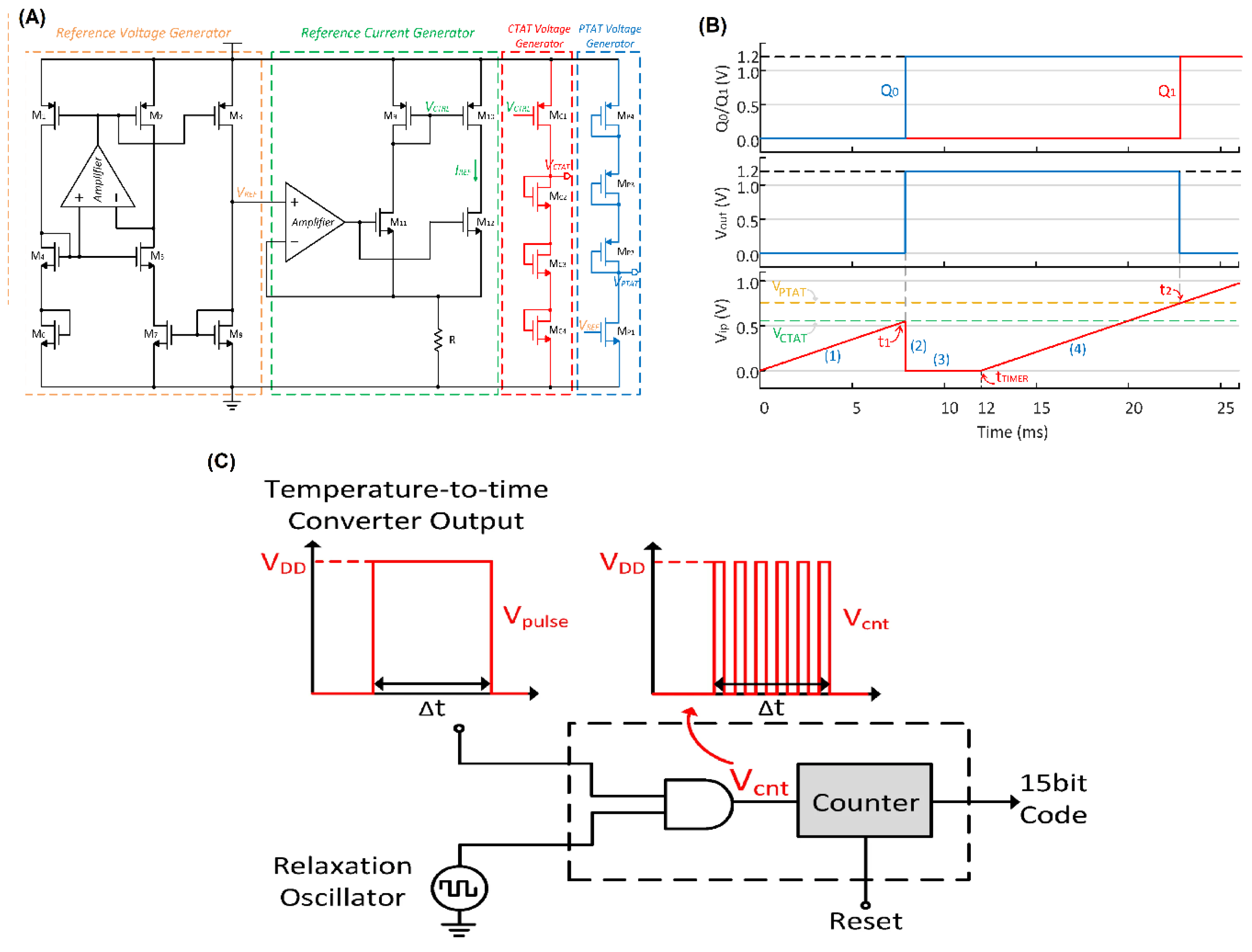
Figure 2.
Temperature-dependent electrical characteristics of power MOSFET devices.(A) Output characteristics of SiC MOSFET under different gate voltages and junction temperatures in the first quadrant.(B) Output and transfer characteristics in the third quadrant under various gate biases and temperatures.(C) Temperature dependence of equivalent resistance and combined resistance extracted under different conduction modes.(D) Equivalent structural models of SiC MOSFETs operating in the first and third quadrants, including internal resistance components.(E) Extraction of ON-state resistances Rds, Rsd, and body diode parameters Rbd, Vbd across temperatures using datasheet-based current–voltage characteristics [28].
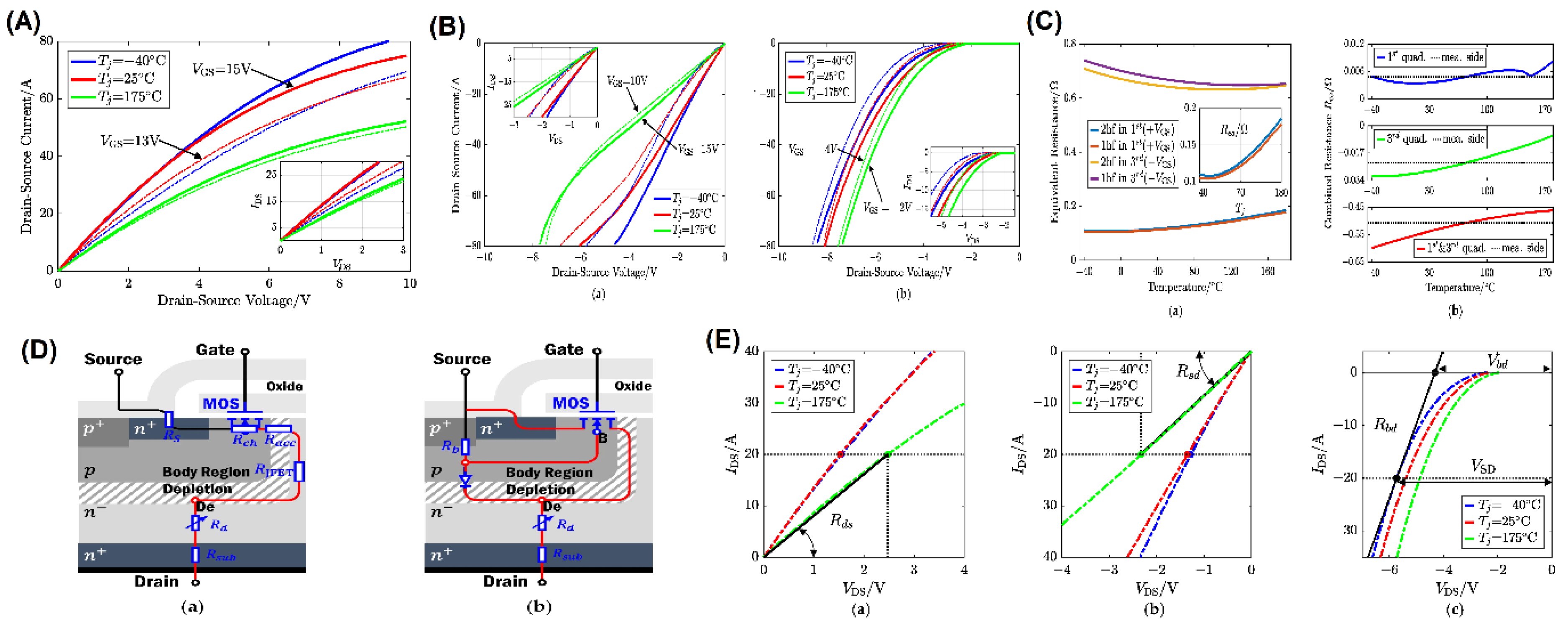
Figure 3.
Circuit-level implementation of a CMOS temperature sensor (A) Temperature sensor architecture comprising sensing, voltage-to-frequency, and frequency-to-digital conversion stages.(B) PTAT² current source and generation of PTAT and reference voltages with corresponding temperature characteristics.(C) Self-biased PTAT current source based on the Oguey topology with enhanced supply rejection.(D) Temperature sensing unit integrating start-up, PTAT current generation, and voltage generation blocks.(E) Differential delay cell used in the voltage-controlled oscillator [31].
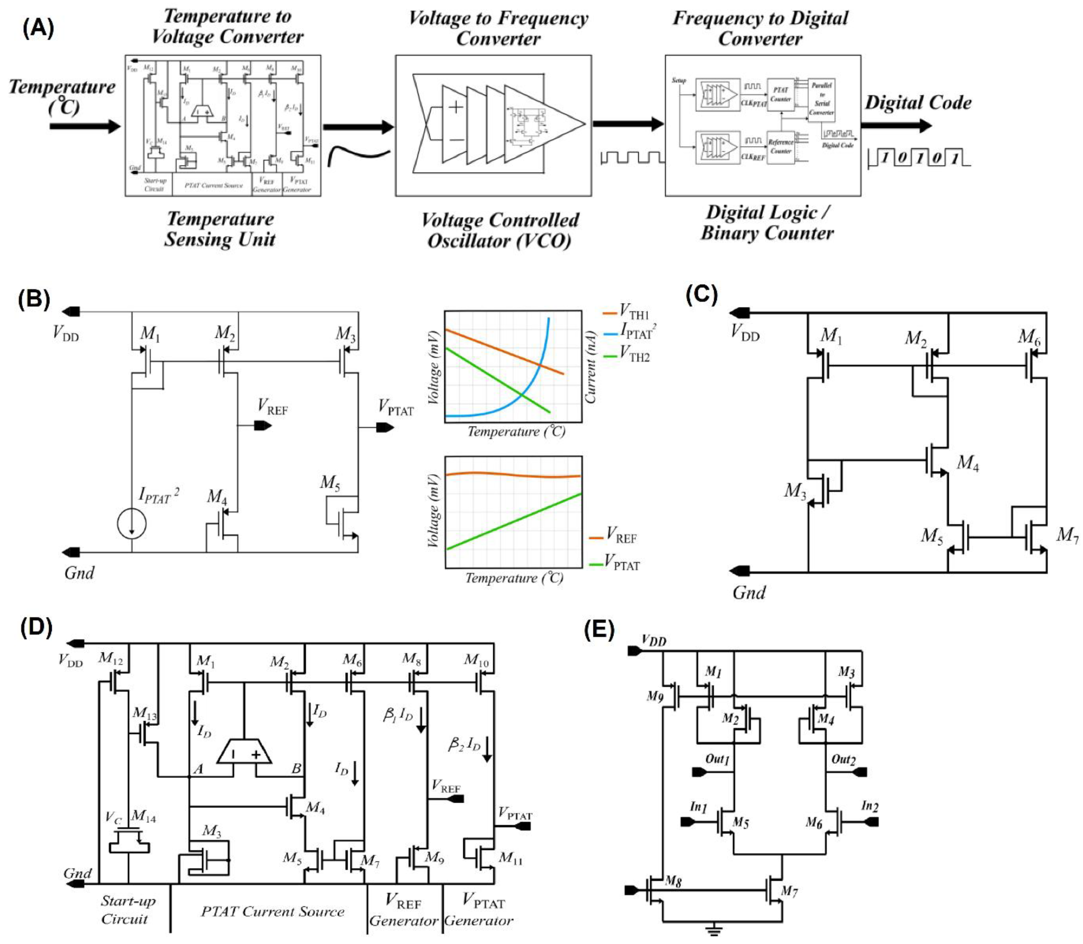
Figure 4.
Impact of TSV-induced thermal stress on stress distribution.(A) Geometric model of a single through-silicon via (TSV) used for thermal stress simulation under axisymmetric boundary conditions.(B) Distribution of thermal stress components in the TSV structure: (a) von Mises stress, (b) radial stress, (c) axial stress, and (d) shear stress.(C) Functional relationship between biaxial strain and threshold voltage shift based on deformation potential theory.(D) Contour plots of carrier mobility variations induced by thermal stress: (a,c) electron and (b,d) hole mobility in the and crystal orientations, respectively.(E) Output characteristics of NMOS and PMOS devices near TSV under different channel orientations and gate voltages: (a) NMOS , (b) NMOS , (c) PMOS, and (d) PMOS [34].
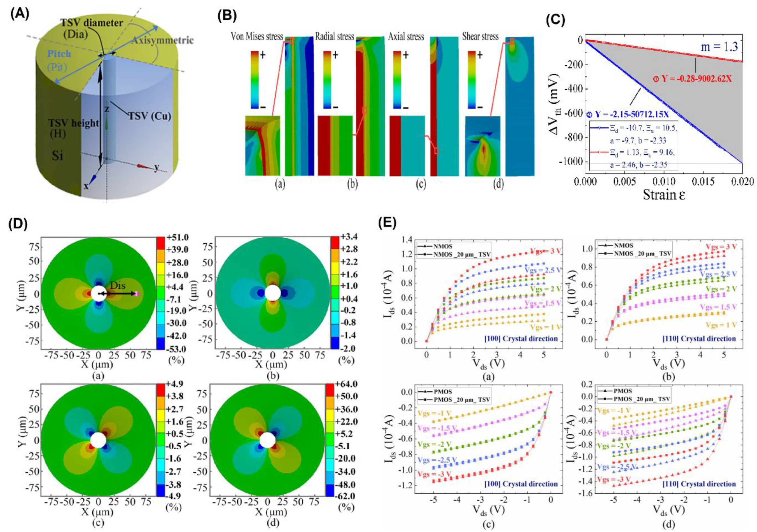
Figure 5.
CDS readout architecture with OPAMP performance and resistor emulation.(A) CDS-based potentiometric readout structure using resistor emulators for input and feedback paths.(B) Two-stage CMOS telescopic OPAMP with cascode configuration for low-noise amplification.(C) OPAMP performance plots: (a) AC gain versus frequency, (b) DC transfer characteristics, and (c) output noise spectrum.(D) Switched-capacitor resistor emulator implementation for (a) feedback path and (b) input path [48].
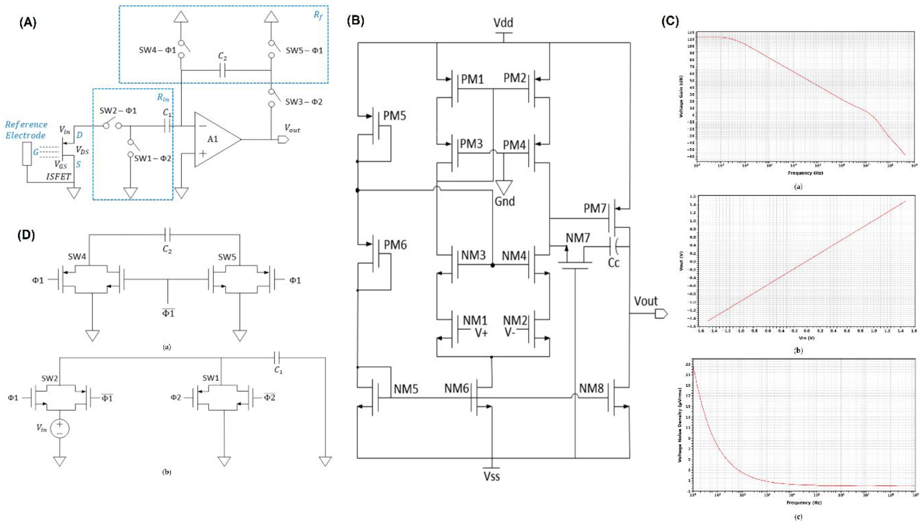
Disclaimer/Publisher’s Note: The statements, opinions and data contained in all publications are solely those of the individual author(s) and contributor(s) and not of MDPI and/or the editor(s). MDPI and/or the editor(s) disclaim responsibility for any injury to people or property resulting from any ideas, methods, instructions or products referred to in the content. |
© 2025 by the authors. Licensee MDPI, Basel, Switzerland. This article is an open access article distributed under the terms and conditions of the Creative Commons Attribution (CC BY) license (http://creativecommons.org/licenses/by/4.0/).
Copyright: This open access article is published under a Creative Commons CC BY 4.0 license, which permit the free download, distribution, and reuse, provided that the author and preprint are cited in any reuse.


