
Submitted:
23 December 2025
Posted:
25 December 2025
You are already at the latest version
Abstract
This work presents an ultra-compact three-way power splitter designed for photonic integrated circuits using topology optimization driven by a custom-developed genetic algorithm. The proposed approach enables global shape reconfiguration within a confined footprint of only 1.88 λ² (λ = 1550 nm), while maintaining high transmission uniformity and minimal mode mismatch. Nearly equal power splitting is achieved with output arms separated by approximately 90°. After gradient-based refinement, the splitter reaches a total transmission efficiency of 90.6%, with only 3.75% reflection and 5.65% radiation losses. This paper constitutes the first reported demonstration of sharp angle three-way power splitting within a sub-2 λ² footprint in a low index contrast (εᵣ ≈ 4.0) platform (such as Si₃N₄-on-SiO₂) through a single jointly optimized junction region. A minimum feature size of 125 nm ensures full compatibility with standard lithography and current fabrication techniques. This approach therefore offers a robust and fabrication-friendly solution for next generation high density power-divider systems.
Keywords:
artificial intelligence
; genetic algorithm
; photonic integrated circuits
; power splitter
1. Introduction
Studies performed over the recent years show a notable variation and creativeness in the designs of T-junctions and in general N-way power splitters for small optical devices. Particularly, ultra-compact Y- and T-junction dividers, optimized utilizing algorithms assisted by artificial intelligence on the LNOI (lithium niobate on insulator) platform, have attracted great interest (Xu et al. 2023). Another research group has reported a low-loss and small dual-mode splitter combining Y-junction, multimode interferometer, and routing coupler (Long et al. 2024). Similarly, a plasmonic power divider defined by a broadband and 3 dB output within a metal-dielectric-metal structure has been proposed (Wahsheh 2021). Concurrently, it has been demonstrated that high terahertz applications of T-, Y-, and E-junction designs made of 2D photonic crystals can attain great efficiency (Geerthana et al. 2023). In addition, an ultra-wideband and adjustable splitter incorporating a SB₂Se₃ doped Y-junction has been realized (Su et al. 2023), while reconfigurable three-way energy dividers have been implemented using topological structures (Makwana and Chaplain 2019). Overall, the geometric tailoring of the optical medium enables the adiabatic transformation of the three-way splitter into a wave steerer around sharp angle bends.
All of the above-mentioned researches provide major developments in the field of small optical power dividers, providing methods that optimize space use, lower losses, and improve manufacture within modern photonic systems. And, fundamental part of dividers requires beam steering which is a more specific topic in photonic applications. In this manner, multimode waveguide (MMW) bends allow flexible and tightly packed configurations within mode-division multiplexing (MDM) based photonic integrated circuits (PICs). Achieving ultra-compact designs without compromising performance remains a major challenge (Cheng et al. 2024; Liao et al. 2024; Liu et al. 2024; Lan et al. 2025; Zhou et al. 2025). High-order modes suffer increased radiation and scattering losses when the bending radius decreases, ascribed to reduced optical confinement and a stronger interaction with waveguide flaws (Bogaerts et al. 2012; Bogaerts and Chrostowski 2018; Sun et al. 2022). Sharp bends especially show the impacts since a significant mode mismatch between straight and curved sections causes increased insertion loss (IL) and inter-mode crosstalk (CT) (Liu et al. 2019; Li et al. 2020; Li et al. 2022). (MDM) has recently become a powerful method for significantly increasing the data transmission capacity of optical communication networks. Multiple orthogonal modes help to transport different data streams inside a single multimode waveguide, therefore improving bandwidth efficiency and integration density. Apart from MMWs, single mode waveguides (SMWs) suffer from radiation losses even more especially through sharp waveguide bends. This type of loss increases if the refractive index of the waveguide is relatively low.
Several approaches have been reported to address these issues on both MMWs and SMWs. A graded index distribution has been proposed as a key factor on beam bending (Oner et al. 2013). Notably, sub-wavelength grating (SWG) (Xu and Shi 2018; Wu et al. 2019) and transformation optics (TO) (Gabrielli et al. 2012; Li et al. 2020) methods possess the ability to improve mode matching, although they often require complex fabrication procedures. These techniques may show restrictions in their capacity to generate ultra-compact design, otherwise the optimization of trajectories using Bezier (Jiang et al. 2018) or Euler (Wu et al. 2018) curves, presents solutions more fit for production. Dual Bezier curve-based MWBs obtained using particle swarm optimization (PSO) maintains low IL and CT by allowing arbitrary-angle bends and numerous transverse electric (TE) modes while still accommodating. These techniques show the possibility for both compactness and great transmission quality; yet, face limitations in handling higher-order mode stability at ultra-small radii. While inverse design approaches using free-form curves (Sun et al. 2021; Chen et al. 2023) or topology optimization (Tsuji et al. 2006; Iguchi et al. 2018) show great compactness and performance gains, they may need computationally intensive processes and yield structures with insufficient fabrication tolerance.
Regarding all of the improvements on beam bending and power splitting methodology, the authors have found topological optimization by artificial intelligence-based algorithms as a preferable technique on ultra-compact optical device designs. More effectively than alternative optimization methods (Frandsen et al. 2014; Pita et al. 2018; Ji et al. 2023), topological optimization helps to reach outstanding performance within limited dimensions. This is mostly justified by its ability to offer, in compared to other approaches, an extraordinarily large range of design choices. Combining this approach with a genetic algorithm helps extremely large number of combinations converge towards a global optimum. Moreover, topological optimization goes beyond conventional (analog) design paradigms at a given resolution level to incorporate improved digital design prospects. This is aptly shown by the research reported in (Jensen and Sigmund 2011). As the study shows, the first (original) design only reflects one of numerous possible results in the field of topologically optimal pairings. By means of design variable change, a better result was obtained, displaying above conventional design performance.
Despite the significant progress reported in compact power splitters and waveguide bending strategies, achieving simultaneous equal power division and sharp-angle output routing within a deeply sub-wavelength footprint remains an unresolved challenge, particularly for low-index-contrast photonic platforms such as Si₃N₄-on-SiO₂. Existing approaches typically rely on extended adiabatic bends, auxiliary routing sections, or symmetry-breaking lattices, which inevitably increase the device footprint or compromise transmission uniformity. In contrast, this work introduces a topology-optimized three-way power splitter that integrates power splitting and beam steering into a single, jointly optimized junction region, enabling approximately 90-degree output separation within an ultra-compact footprint of only 1.88 λ². To the best of the authors’ knowledge, this represents the first demonstration of sharp-angle three-way power splitting realized in a low-index-contrast (ε ≈ 4) integrated photonic platform, while maintaining near-equal transmission and fabrication-feasible feature sizes. The proposed design therefore establishes a new design regime for dense photonic integration, where compactness, angular routing, and transmission efficiency are achieved concurrently rather than through trade-offs. The organization of this work is as follows: Section 2 clarifies the problem and suggested design approach. Section 3 covers the simulation setup, tackles performance evaluation and present the consequent comparison. Finally, Section 4 offers final remarks.
2. Materials and Methods
2.1. Three-Way Power Splitter
A standard N-way power splitter consists of an input waveguide and N-output waveguides which is an essential passive part of many optical communication systems, especially photonic integrated circuits (PICs). Its main job is to equally split an incoming optical signal into N-output pathways. In order to facilitate signal distribution, monitoring, and processing across many optical systems, this division is essential. The optical devices that splitters widely used are input power distributors, passive optical networks, optical switches / routers, optical coupling input and output interfaces and many other subsystems.
Just as electronic circuit sizes become smaller by time, optical circuits also experience the same trend. Therefore, a fundamental problem of current PIC technology lies beneath compactness limits. In this manner, three-way power splitters dramatically suffer from a trade-off between splitter performance and device size. Let us consider a standard device given by Figure 1. In such a design, the determining factor in terms of size is the radius of curvature of the output waveguides, namely . Even if this radius is chosen as ( is operating wavelength in vacuum), the ratio between H-field intensities of and is over 7.72. This significant difference in output power values directly reveals the need for a specific design in the joint area.
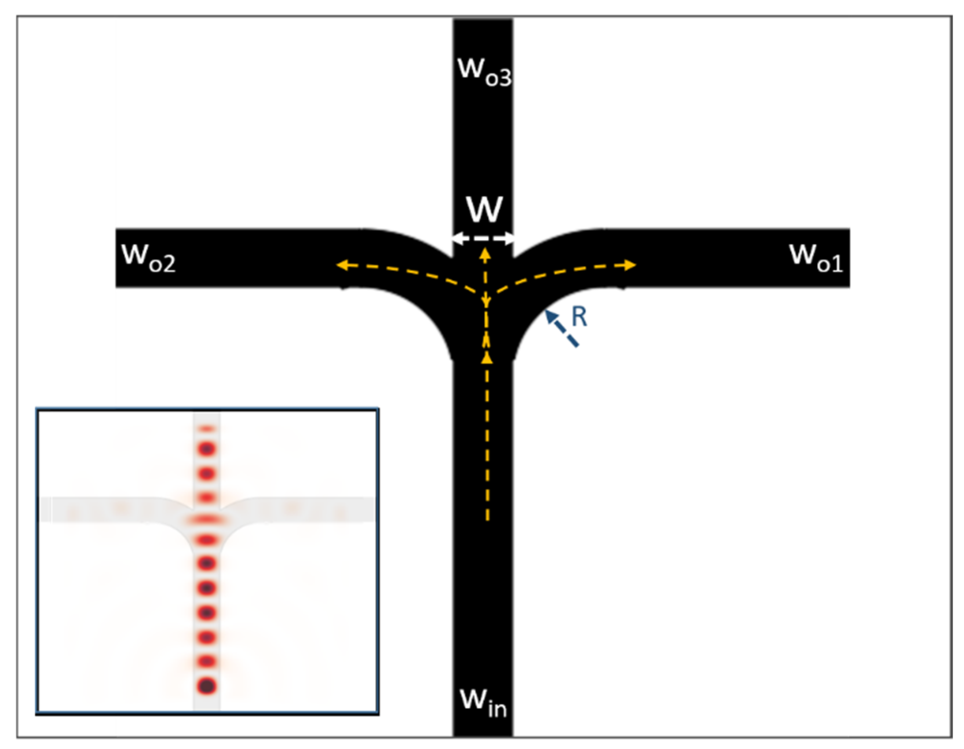
Figure 1.
A standard three-way beam splitter. Waveguide width values of the all input and output waveguides are kept same at with dielectric permittivity values of . Inset shows energy distribution when .
Figure 1.
A standard three-way beam splitter. Waveguide width values of the all input and output waveguides are kept same at with dielectric permittivity values of . Inset shows energy distribution when .
A conventional method utilized in the literature aims to optimize waveguide bends by continuous structures. However, as mentioned in the Introduction Section, these bends mostly can be written in terms of analytical functions. Nevertheless, random topologies generated by artificial intelligence-based designs cover the analytically described bends. In this optimization process, randomness may be introduced by reshaping the topology of the turning area. When only a single material is introduced into the design, and the junction area is fixed to and the resolution of topology to then different designs are possible to generate. Herein, and scale the device size along x and y directions, respectively while n does the same inversely for resolution. As a result, an optimization method is inevitable to achieve a satisfactory performance within a compact splitter.
As mentioned in the Introduction, topological optimizations among the optical device design approaches enable miniaturized subsystems compromising fabrication tolerances. This disadvantage can be overcome by putting constraints on the parameter n in terms of feasibility. In this study, we hold nm in order not to encounter this challenge. Topological reshapes usually generate designs such that multiple extremum points arise as performance which is directly related to the success criteria. In this manner, genetic algorithm (GA) provides remarkably adequate designs since one of its primary advantages is being able to find the global optimum. This superiority has led the optimization methods to be based mostly on GA. Main steps of the algorithm are briefly given in the next Section.
2.2. Genetic Algorithm
A special code for the genetic algorithm was developed (Matlab 2023) by the authors and this code was integrated with MEEP (Oskooi et al. 2010) which is based on finite-difference time-domain methodology. Below is an outline of the proposed algorithm:
i) An initial population is created totally randomly within the geometric constraints of the design. Both number of candidates and maximum number of generations are determined to be 100.
ii) When each cycle is completed, the performance values (output waveguide transmitted powers) of the parameters of the solution candidates are computed.
iii) The next step is aimed at determining the selection criteria and subsequent crossover process. One of the standard methods, the “random gene mixing” method, is used. In addition to this method, the probability of a successful design to transfer parameters to the next generation is increased proportionally with respect to its performance value. The next generation is created from these new and randomly selected parameters, preserving the population size. In each iteration, each parameter transfer is given a 2% chance of mutation. This eliminates the dependence of the output design on only the first-generation parameters.
iv) The algorithm automatically terminates itself when it reaches the target number of generations or the target success.
3. Results and Discussion
The data obtained by implementing the methodology given in Subsection 3.2 is represented and discussed below. Figure 2 shows the results of the algorithm. Figure 2(a) displays the results of each individual under the optimization performed. The initial population of 100 individuals was run until it reached 100 generations, again with 100 individuals in each generation. The success of the process can be seen in Figure 2(b). Here, each point gives the arithmetic mean performance values of its own generation. An average success ratio of 10% is obtained by random initial parameters and the plot tends to saturate below 60% at first within 20 generations if mutation probability doesn’t exist. However, it finally increases up to 80% by introducing mutation.
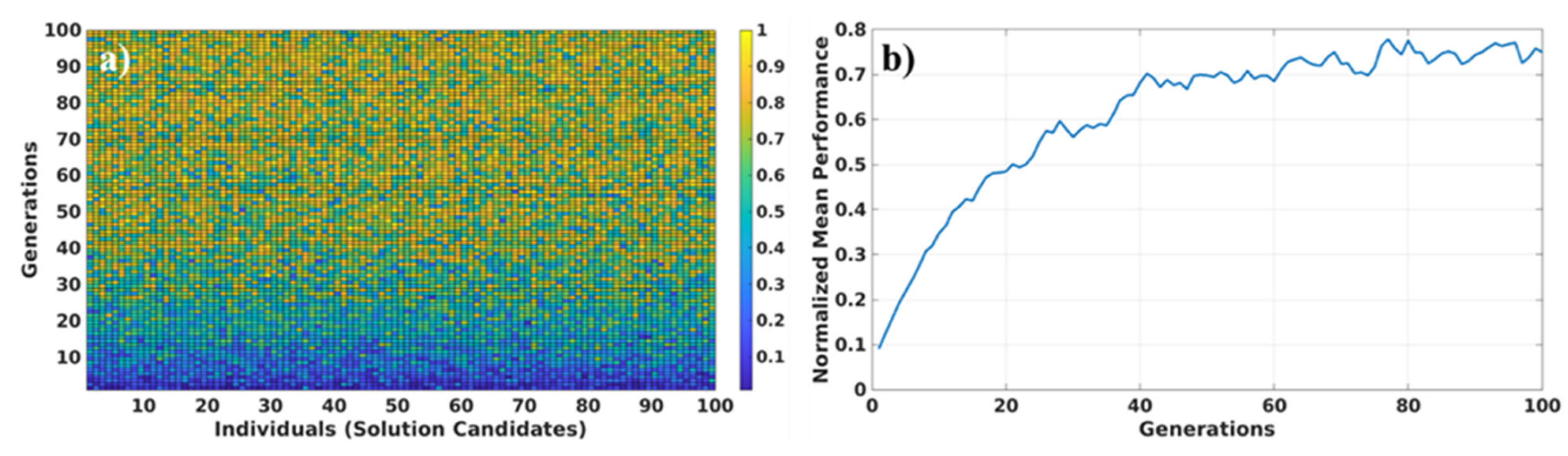
Figure 2.
(a) The performance of each solution candidate across 100 generations is exhibited in a normalized format. (b) The average performance of each generation is plotted in a normalized fashion. Both normalizations are taken relative to the best-performing solution candidate of all.
Figure 2.
(a) The performance of each solution candidate across 100 generations is exhibited in a normalized format. (b) The average performance of each generation is plotted in a normalized fashion. Both normalizations are taken relative to the best-performing solution candidate of all.
Parameters corresponding to the best result of the GA is considered for time-domain simulations. Dielectric permittivity is which is compatible with Si3N4 low-loss waveguides (Bauters et al. 2011). The resolution of topology is and scaling factors are and . Hence, total junction area is ~ . If the operating vacuum wavelength is chosen as nm, then the width of all waveguides becomes ~ nm.
Figure 3(a) shows the finalized junction geometry of three-way power splitter which is symmetrical with respect to x-axis. The waveguides and are tilted 2° after the GA optimization to perfectly eliminate mode-misalignment. When the field energy values transmitted to the waveguides at the points taken on the and cross-sections are compared, their similarity is at a rate of ~93%. This value is below 7% when standard approach as given in the inset of Figure 1 with and total junction size of .
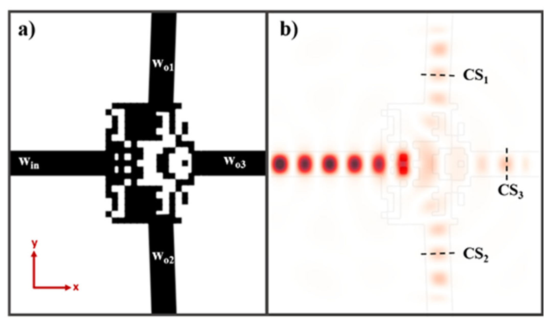
Figure 3.
(a) The resulting geometry of the best solution is shown. (b) The time-averaged field energy density () under steady-state condition.
Figure 3.
(a) The resulting geometry of the best solution is shown. (b) The time-averaged field energy density () under steady-state condition.
When evaluated in respect to their main functionality and design approach, this work shows the best degree of resemblance to the cited study (Xu et al. 2023). Particularly, the Y- and T-type splitters included in that work show . (2.60 μm × 2.60 μm) and (2.85 μm × 4.94 μm), respectively. Still, should a 90-degree T-type three-way splitter be required, such splitters call for an additional layer in the design. Usually matching the number of outputs, the demand increases in line with N for N-way splitters. Conversely, the present research reveals that one can construct a geometry very well-suited for N-way splitting configurations by generalizing the suggested design process.
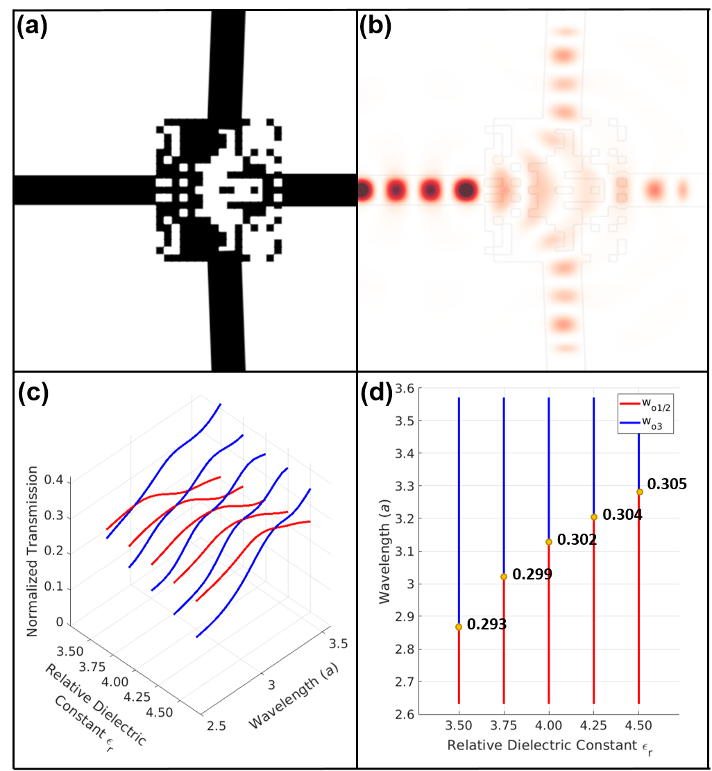
A power loss of approximately 30% due to reflection and radiation has been computed through MEEP program. This indicates the necessity of an additional optimization step in the design. In this context, the cross-sectional size of the structure was increased to 1.88 times the square of the wavelength () by expanding the dimensions in the x-direction by and in the y-direction by . A gradient-based topology optimization was then applied. As part of this iterative process, the performance impact of placing a single dielectric block (represented by a black square) with a dielectric constant of 4 at different x-y positions outside the structure was evaluated. The best result obtained from this configuration was then adopted as the new design, and the iteration was repeated. A similar process was also applied to the vacuum regions (represented by white squares) within the geometry. The updated structural schematic and corresponding energy density are shown in Figure 4(a) and 4(b). In the new splitter structure, the output field distributions maintain similarities, with transmission efficiencies for and being 30.2%. Only, 3.75% of the input power is reflected from the win-junction interface and 5.65% is radiated. Thus, the three-way splitter successfully distributes 90.6% of the input power equally among three arms while preserving the amplitude distributions at the waveguide inputs.
Finally, effects of different refractive index contrasts and wavelength were analyzed to show robustness of the design (please see Figs. 4(c) and 4(d)). Change of the refractive index leads a shift on operating wavelength however wavelength units are given by “” which can be scaled to match 1550 nm optical communication wavelength and this scaling should be reflected on the blocks that have sizes of .
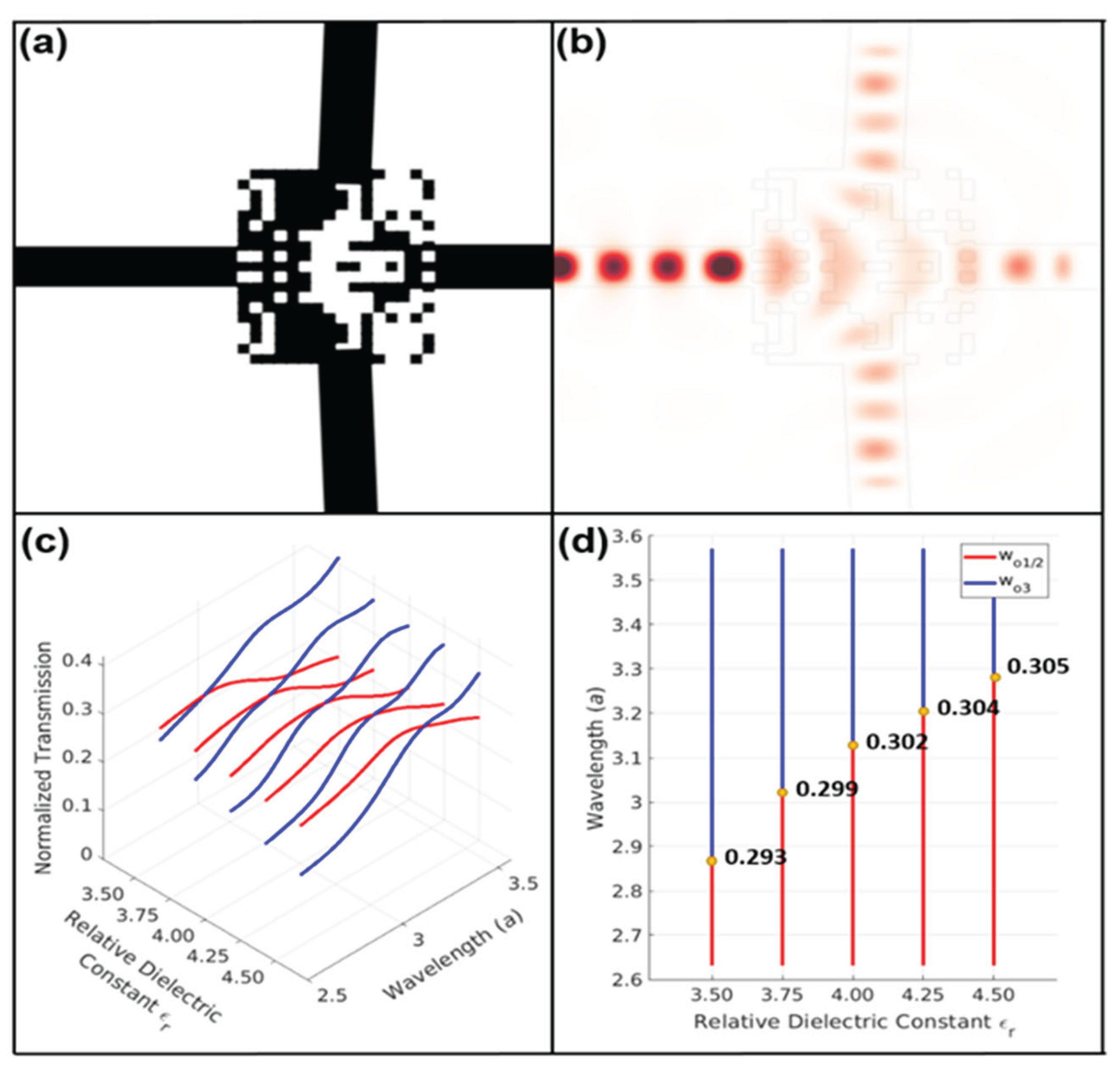
Figure 4.
(a) The resulting geometry of the final structure after gradient-based topology optimization is shown. (b) The time-averaged field energy density () under steady-state condition. (c) and transmission efficiencies with respect to wavelength for different dielectric constants are given and in (d) normalized efficiency values that matches equally for all waveguides are plotted.
In this work, we present a 1×3 power splitter in which the three output waveguides are separated by almost 90 degrees with a major challenge addressed of wave-bending within a minimal footprint. Indeed, a survey of the literature shows that direct 90-degree branching in 1×N power splitters is rarely observed; alternatively, realizing 90-degree output bending typically requires device dimensions several times larger than the operating wavelength. In other words, the optimization conducted here simultaneously ensures both efficient power splitting and sharp wave bending within a compact area. Nevertheless, a comparison with existing 1×N power splitters in the literature can still be made. For example, a 1×2 power splitter has been reported that achieves a 50:50 power division with a coupling length greater than 10 µm and operates over the 1480–1585 nm range (Ozcan et al. 2023). In another paper, researchers have proposed a novel 1×3 power-splitter concept based on the plane-wave expansion method (Makwana and Chaplain 2019). Their central idea is to modify the band diagrams by breaking the full symmetry of a square lattice. Considering the dimensionless parameters presented in the study, the total device footprint corresponds to approximately 3.65 λ². Although the authors state that the device operates over a broadband range, a specific bandwidth interval is not explicitly provided. A remarkable result has been published regarding a 1×2 power splitter with a footprint of 1.50 λ², operating between 1500 nm and 1600 nm, where the output power division remains between 30% and 50% (Piggott et al. 2020). The same reference also reports a 1×3 wavelength demultiplexer with a footprint of 10.3 λ², whose insertion losses for the three output channels are 3.0 dB at 1500 nm, 3.1 dB at 1540 nm, and 1.2 dB at 1580 nm. Finally, existing 1×3 power-splitter designs with a footprint of around 3.96 λ² operate in the 1450–1600 nm range. When equal power division is considered as the performance criterion, the best transmission, approximately 30%, is achieved near 1540 nm, whereas the difference between transmission values at lower and higher wavelengths can reach up to 7%.
Topologically optimized photonic designs often involve small, challenging to fabricate elements. As a result, most past experimental demonstrations have relied on high-resolution techniques such as electron-beam lithography or focused ion beam machining, which are accurate (Piggott et al. 2020). Electron beam lithography and ion-beam milling have typical resolutions of about 10 and 30 nm, respectively. On the other hand, photolithography techniques have usually offer worse resolution ranging from 500 to 65 nm which can be improved up to 20 nm by EUV lithography. In our design we especially kept our resolution at which is compatible with all fabrication methods.
From the perspective of physical dimensions, our solution stands out mostly for its ability to achieve efficient beam steering around steep bends, even in low refractive index contrast. Although a strong transmission across two different frequency bands through an analytically well-defined graded refractive index function, it has been showed that the structure lacks sufficient compactness (Oner et al. 2019). In a similar line, a recent work has achieved high-efficiency bending across several optical modes by means of analytically determined Bezier-shaped curves (Zhou et al. 2025). Still, the construction's dimensions remain larger than that of desired by PIC designs. Finally, when considering all the performance parameters required for a junction region, the geometry proposed in this paper demonstrates superiority.
Additionally, from a practical standpoint, sharp 90° waveguide bends are often regarded as challenging due to potential scattering losses and lithographic limitations. In a previous study, small 90° waveguide bends have been experimentally created using geometries that are optimized for CMOS fabrication with current lithography and etching techniques (Song et al. 2020). This indicates that advanced bend shaping can attain low-loss performance while maintaining compatibility with conventional PIC processes (Chen et al. 2025).
4. Conclusions
This research addresses reducing the size of the junction area of power splitters in photonic integrated circuits. A novel N-way splitter design technique based on topology optimization via a custom-developed genetic algorithm is proposed. Our method efficiently preserves strong optical confinement within an ultra-compact junction area, even though light confinement and beam steering are particularly challenging in relatively low refractive index platforms. The optimized geometry reduces both radiation and scattering losses by combining smooth field evolution with global shape modification.
An input power carried by the transverse electric fundamental mode is divided into approximately 90-degree-separated, nearly equal three output channels through an ultra-compact structure with an extremely small footprint of only 1.88 λ². The similarity of output waves is enhanced by more than 13 times compared to a standard divider with an even larger geometry. To the best of the authors’ knowledge, no previously reported 1×3 splitter simultaneously demonstrates (i) direct ~90° branching, (ii) a sub-2 λ² footprint, (iii) compatibility with low-index material platforms, and (iv) fabrication-feasible feature sizes, even in purely numerical form. These results can be directly implemented in practical applications such as optical chip input power dividers based on Si₃N₄ waveguides on SiO₂ substrates. The minimum feature size of 125 nm ensures full compatibility with standard photolithography as well as advanced fabrication techniques. In addition, the scalability of Maxwell’s equations enables the structure to operate in the microwave regime, where experimental studies can be carried out using low-loss and readily available commercial-off-the-shelf materials (e.g., TPU and θ-phase alumina) with similar permittivity values (). This approach therefore provides a strong, fabrication-friendly solution for next-generation high-density power-divider systems.
Author Contributions
The following statements should be used “Conceptualization, ALP and ONER.; methodology, ALP and ONER.; software, ONER; validation, ALP and ONER; formal analysis, ALP and ONER; investigation, ALP; resources, ALP and ONER; writing—original draft preparation, ALP and ONER.; writing—review and editing, ALP and ONER; visualization, ALP and ONER. All authors have read and agreed to the published version of the manuscript.”
Funding
The authors have not disclosed any funding
Data availability
The datasets analyzed during the current study available from the corresponding author on reasonable request.
Conflicts of Interest
The authors declare no conflicts of interest.
References
- Bauters, J., Heck, M., John, D., Dai, D., Tien, M., Barton, J., Leinse, A., Heideman, R., Blumenthal, D., Bowers, J.: Ultra-low-loss high-aspect-ratio Si₃N₄ waveguides. Opt. Express 19, 3163–3174 (2011). [CrossRef]
- Bogaerts, W., Chrostowski, L.: Silicon photonics circuit design: methods, tools and challenges. Laser Photonics Rev. 12, 1700237 (2018). [CrossRef]
- Bogaerts, W., De Heyn, P., Van Vaerenbergh, T., De Vos, K., Selvaraja, S.K., Claes, T., Baets, R.: Silicon microring resonators. Laser Photonics Rev. 6, 47–73 (2012). [CrossRef]
- Boyd, R., Prato, D.: Nonlinear Optics. Academic Press, Burlington (2008).
- Butt, M.A., Juchniewicz, M., Słowikowski, M., Kozłowski, Ł., Piramidowicz, R.: Mid-infrared photonic sensors: Exploring fundamentals, advanced materials, and cutting-edge applications. Sensors 25, 1102 (2025). [CrossRef]
- Castellan, C., Trenti, A., Vecchi, C., Marchesini, A., Mancinelli, M., Ghulinyan, M., Pucker, G., Pavesi, L.: On the origin of second harmonic generation in silicon waveguides with silicon nitride cladding. Sci. Rep. 9, 1088 (2019). [CrossRef]
- Chen, J., Zheng, Z., Zhang, C.: Low-loss waveguide bend for compact and broadband photonic integrated circuits. Opt. Lett. 50, 7360–7363 (2025). [CrossRef]
- Chen, Y., Qiu, J., Dong, Z., Wang, L., Liu, Y., Guo, H., Wu, J.: Inverse design of free-form devices with fabrication-friendly topologies based on structure transformation. J. Lightwave Technol. 41, 4762–4776 (2023). [CrossRef]
- Cheng, C., Yang, S., Liu, W., Liu, S., Huo, Y., Fu, X., Yang, L.: Ultra-compact inverse designed multimode waveguide bend based on levelset method. IEEE Photonics Technol. Lett. 36, 571–574 (2024). [CrossRef]
- Frandsen, L.H., Elesin, Y., Frellsen, L.F., Mitrovic, M., Ding, Y., Sigmund, O., Yvind, K.: Topology optimized mode conversion in a photonic crystal waveguide fabricated in silicon-on-insulator material. Opt. Express 22, 8525–8532 (2014). [CrossRef]
- Gabrielli, L.H., Liu, D., Johnson, S.G., Lipson, M.: On-chip transformation optics for multimode waveguide bends. Nat. Commun. 3, 1217 (2012). [CrossRef]
- Geerthana, S., Sridarshini, T., Balaji, V.R., Sitharthan, R., Madurakavi, K., Thirumurugan, A., Dhanabalan, S.S.: Ultra compact 2D-PhC based sharp bend splitters for terahertz applications. Opt. Quantum Electron. 55, 778 (2023). [CrossRef]
- Iguchi, A., Tsuji, Y., Yasui, T., Hirayama, K.: Topology optimal design for optical waveguides using time domain beam propagation method. IEICE Electron. Express 15, 20180417 (2018). [CrossRef]
- Jensen, J.S., Sigmund, O.: Topology optimization for nano-photonics. Laser Photonics Rev. 5, 308–321 (2011). [CrossRef]
- Ji, W., Chang, J., Xu, H.X., Gao, J.R., Gröblacher, S., Urbach, H.P., Adam, A.J.L.: Recent advances in metasurface design and quantum optics applications with machine learning, physics-informed neural networks, and topology optimization methods. Light Sci. Appl. 12, 169 (2023). [CrossRef]
- Lan, Y., Liu, S., Cheng, C., Chen, X., Fu, X., Yang, L.: Ultra-compact multimode waveguide bends with arbitrary bending angles. Opt. Express 33, 13133–13144 (2025). [CrossRef]
- Li, F., Ding, F., Wu, R., Liu, Y., Xu, K.: Compact four-mode silicon multimode bends with a 500 nm bandwidth. In: Proc. OECC 2023, Shanghai, China, pp. 1–3 (2023). [CrossRef]
- Li, S., Cai, L., Gao, D., Dong, J., Hou, J., Yang, C., Chen, S., Zhang, X.: Compact and broadband multimode waveguide bend by shape-optimizing with transformation optics. Photonics Res. 8, 1843–1849 (2020). [CrossRef]
- Liao, J., Tian, Y., Yang, Z., Xu, H., Dai, T., Zhang, X., Kang, Z.: Broadband and compact silicon multimode waveguide bends based on hybrid shape optimization. J. Lightwave Technol. 42, 4882–4891 (2024). [CrossRef]
- Liu, S., Niu, J., Huo, Y., Cheng, C., Fu, X., Yang, L.: Ultra-compact and fabrication-tolerant multimode photonic jumpers based on dual Bezier curves. Opt. Lett. 49, 3352–3355 (2024). [CrossRef]
- Liu, Y., Xu, K., Wang, S., et al.: Arbitrarily routed mode-division multiplexed photonic circuits for dense integration. Nat. Commun. 10, 3263 (2019). [CrossRef]
- Makwana, M.P., Chaplain, G.: Tunable three-way topological energy-splitter. Sci. Rep. 9, 18939 (2019). [CrossRef]
- Oner, B.B., Turduev, M., Kurt, H.: High-efficiency beam bending using graded photonic crystals. Opt. Lett. 38, 1688–1690 (2013). [CrossRef]
- Oskooi, A.F., Roundy, D., Ibanescu, M., Bermel, P., Joannopoulos, J.D., Johnson, S.G.: MEEP: A flexible free-software package for electromagnetic simulations by the FDTD method. Comput. Phys. Commun. 181, 687–702 (2010). [CrossRef]
- Ozcan, C., Aitchison, J.S., Mojahedi, M.: Foundry-processed compact and broadband adiabatic optical power splitters with strong fabrication tolerance. Photonics 10, 1310 (2023). [CrossRef]
- Piggott, A.Y., Ma, E.Y., Su, L., Ahn, G.H., Sapra, N.V., Vercruysse, D., Vučković, J.: Inverse-designed photonics for semiconductor foundries. ACS Photonics 7, 569–575 (2020). [CrossRef]
- Song, J.H., Kongnyuy, T.D., De Heyn, P., Lardenois, S., Jansen, R., Rottenberg, X.: Low-loss waveguide bends by advanced shape for photonic integrated circuits. J. Lightwave Technol. 38, 3273–3279 (2020). [CrossRef]
- Su, Y., Zhang, Y., Zhou, X., Liu, D., Zhang, M.: Ultra broadband tunable power splitter based on Sb₂Se₃-assisted Y-junction. J. Lightwave Technol. 42, 2817–2822 (2023). [CrossRef]
- Sun, S., Dong, P., Zhang, F., Wang, J., Zhu, N., Shi, Y.: Inverse design of ultra-compact multimode waveguide bends based on free-form curves. Laser Photonics Rev. 15, 2100162 (2021). [CrossRef]
- Sun, S., Yang, Z., Wang, J., Zhang, R., Zhang, F., Zhu, N., Li, Z.: Ultra-sharp silicon multimode waveguide bends based on double free-form curves. Photonics Res. 10, 1484–1490 (2022). [CrossRef]
- The MathWorks, Inc.: MATLAB R2023b. Natick, MA, USA (2023).
- Tsuji, Y., et al.: Design of optical circuit devices based on topology optimization. IEEE Photonics Technol. Lett. 18, 850–852 (2006). [CrossRef]
- Wahsheh, R.A.: Ultra-compact broadband 3-dB metal–dielectric–metal plasmonic power splitter. J. Mod. Opt. 68, 153–160 (2021). [CrossRef]
- Wu, H., Li, C., Song, L., Tsang, H.K., Bowers, J.E., Dai, D.: Ultra-sharp multimode waveguide bends with subwavelength gratings. Laser Photonics Rev. 13, 1800119 (2019). [CrossRef]
- Wu, X., Zhou, W., Huang, D., Zhang, Z., Wang, Y., Bowers, J., Tsang, H.K.: Low crosstalk bent multimode waveguide for on-chip mode-division multiplexing interconnects. In: Proc. Conference on Lasers and Electro-Optics (CLEO), Optica Publishing Group, Paper JW2A.66 (2018). [CrossRef]
- Xu, H., Shi, Y.: Ultra-sharp multi-mode waveguide bending assisted with metamaterial-based mode converters. Laser Photonics Rev. 12, 1700240 (2018). [CrossRef]
- Xu, Q., Liu, J.M., Zhang, D.L., Hua, P.R.: Ultra-compact lithium niobate power splitters designed by an intelligent algorithm. Opt. Laser Technol. 160, 109057 (2023). [CrossRef]
- Zhou, S., Yu, X., Yuan, Q., Sui, X.: Ultra-compact multimode waveguide bend based on a central width controllable dual Bezier structure. Opt. Lett. 50, 1985–1988 (2025). [CrossRef]
Disclaimer/Publisher’s Note: The statements, opinions and data contained in all publications are solely those of the individual author(s) and contributor(s) and not of MDPI and/or the editor(s). MDPI and/or the editor(s) disclaim responsibility for any injury to people or property resulting from any ideas, methods, instructions or products referred to in the content. |
© 2025 by the authors. Licensee MDPI, Basel, Switzerland. This article is an open access article distributed under the terms and conditions of the Creative Commons Attribution (CC BY) license (http://creativecommons.org/licenses/by/4.0/).
Copyright: This open access article is published under a Creative Commons CC BY 4.0 license, which permit the free download, distribution, and reuse, provided that the author and preprint are cited in any reuse.


