Submitted:
29 May 2025
Posted:
30 May 2025
You are already at the latest version
Abstract
Polarization control is of fundamental importance for modern optical systems, and optical polarizers serve as critical components for enabling this functionality. Here, we experimentally demonstrate optical polarizers by integrating 2D molybdenum disulfide (MoS2) films onto silicon photonic waveguides. High-quality monolayer MoS2 films with highly anisotropic light absorption are synthesized via a low-pressure chemical vapor deposition (LPCVD) method and subsequently transferred onto silicon-on-insulator (SOI) nanowire waveguides to fabricate integrated optical polarizers. Detailed measurements are carried out for the fabricated devices with various MoS2 film coating lengths and silicon waveguide geometry. The results show that a maximum polarization-dependent loss of ~21 dB is achieved, together with a high figure of merit of ~4.2. In addition, the hybrid waveguide polarizers exhibit broad operation bandwidth exceeding ~100 nm and excellent power durability. These results highlight the strong potential for on-chip integration of 2D MoS2 films to implement high-performance polarization selective devices.
Keywords:
integrated photonics
; 2D materials
; transition metal dichalcogenides
; optical polarizers
1. Introduction
The control of light polarization plays a crucial role in modern optical systems and underpins a wide range of advanced optical technologies [1,2]. Optical polarizers, which allow transmission of light in a specific polarization while suppressing the orthogonal polarization component, serve as key elements for polarization control in optical systems [3]. To date, a variety of optical polarizers have been developed based on refractive prisms [4,5], birefringent crystals [6,7], fiber components [8,9], and integrated photonic devices [10,11]. However, these polarizers based on bulk materials often struggle to achieve efficient polarization selection over wide wavelength ranges. This limitation is especially significant given the increasing demand for broadband optical polarizers driven by rapid progress in photonic technologies and systems [12,13].
Recently, due to strong anisotropy in light absorption and broadband response, two-dimensional (2D) materials with atomic-scale film thicknesses have been incorporated onto bulk optical waveguides to realize high-performance optical polarizers [14], as demonstrated by those incorporating 2D materials such as graphene [14,15,16], graphene oxide (GO) [17,18,19], and transition metal dichalcogenides (TMDCs) [20,21,22]. As a significant subgroup in the 2D material family, TMDCs exhibit a direct bandgap in their monolayer form that transitions to an indirect bandgap in few-layer or bulk forms [23,24]. This distinctive property facilitates their widespread applications for next-generation atomically thin devices such as transistors [25,26], photodetectors [27,28], and electrocatalysts [29,30]. More recently, the strong anisotropic light absorption of 2D TMDC films across broad wavelength ranges has also been explored, and their integration onto polymer and Neodymium-doped Yttrium Aluminum Garnet (Nd:YAG) waveguides for realizing optical polarizers has been successfully demonstrated [21,22].
In this work, we demonstrate the integration of 2D molybdenum disulfide (MoS2) ‒ a representative TMDC material ‒ onto the widely used silicon photonic platform to realize high-performance optical polarizers. High-quality monolayer MoS2 films with strong anisotropy in light absorption are synthesized via a low-pressure chemical vapor deposition (LPCVD) method, and subsequently transferred onto silicon-on-insulator (SOI) nanowire waveguides using polymer-assisted transfer process. We perform detailed measurements for the fabricated devices with different MoS2 film coating lengths and silicon waveguide geometry, achieving a maximum polarization-dependent loss of ~21 dB and a high figure of merit of ~4.2. In addition, the hybrid waveguide polarizers exhibit broad operation bandwidth over ~100 nm and excellent power durability. Finally, we compare the performance of our device with state-of-the-art waveguide polarizers incorporating different 2D materials and find that it achieves the highest figure of merit (FOM) among all those based on the silicon photonic platform. These results reveal the strong potential of 2D TMDC films for implementing high-performance integrated polarization selective devices.
2. Device Design
As an important member of the TMDCs family that has been widely studied, MoS2 features a hexagonal sheet of molybdenum (Mo) atoms sandwiched between two hexagonal sheets of sulfur (S) atoms [31,32]. Figure 1(a) illustrates the atomic structure of monolayer MoS2, where Mo and S atoms are connected by strong covalent bonds. Multi-layered MoS₂ consists of vertically stacked layers that are weakly bonded through van der Waals interactions [26]. Monolayer MoS2 has shown great potential as a semiconducting material with a direct bandgap of ~1.8 – 1.9 eV [33]. This is larger than the energy of two photons at 1550 nm (i.e., ~1.6 eV), which allows for relatively low linear light absorption as well as two-photon absorption at near infrared wavelengths. The quality of 2D MoS2 crystals plays a crucial role in determining the material properties such as refractive index, light absorption, and optical bandgap, which correlates to the intrinsic structural defects induced by sulfur vacancies [34,35]. In this work, we choose MoS2 to implement optical polarizers due to several compelling advantages. First, it exhibits strong anisotropic light absorption over a very broad spectral bandwidth [36,37]. Second, it possesses relatively low linear absorption in the infrared regime, with an extinction coefficient nearly 1 order of magnitude lower than that of graphene [38,39], making it particularly suitable for infrared photonic applications. Finally, we develop a simple and one-step chemical vapor deposition (CVD) method to fabricate MoS2 films with precise control over structural defects [34], which allows us to tailor the intrinsic optical properties of MoS2 for specific optical applications.
Figure 1(b) shows the schematic of an integrated waveguide polarizer consisting of a silicon nanowire waveguide coated with a monolayer MoS2 film. Similar to other 2D materials such as graphene and graphene oxide (GO) [14,15,17,19], 2D MoS2 films exhibit strong anisotropic optical absorption [40,41], with significantly higher absorption for light propagating in the in-plane direction compared to the out-of-plane direction. For the hybrid waveguide in Figure 1(b), these directions correspond to TE- and TM-polarized incident light, respectively. As a result, the hybrid waveguide can effectively operate as a TM-pass waveguide polarizer. It is worth noting that 2D MoS₂ exhibits a broad spectral range of material anisotropy spanning from visible to infrared wavelengths [36]. This wide bandwidth offers a significant advantage for MoS₂-coated integrated waveguide polarizers, which is difficult to achieve for conventional bulk silicon photonic polarizers [1,14,42].
Figure 1(c) shows a schematic of the cross section of the hybrid waveguide in Figure 1(b). The corresponding transverse electric (TE) and transverse magnetic (TM) mode profiles at 1550 nm are provided in Figure 1(d), which were simulated using commercial mode-solving software (COMSOL Multiphysics). In our simulation, the thickness of the monolayer MoS2 film was ~0.7 nm. The refractive index (n) and extinction coefficient (k) of MoS2 for TE polarization were nTE = ~3.8 and kTE = ~0.107, respectively. For TM polarization, the corresponding values were nTM = ~3.2 and kTM = ~0.027. These values were obtained from our measurements in the following sections. The simulated TE- and TM polarized effective indices for the hybrid waveguide were ~2.081 + 3.313 × 10⁻⁴i and ~1.551 + 7.132 × 10⁻⁵i, respectively. The large difference in the imaginary part highlights the polarization selectivity for the hybrid waveguide, which originates from the significant disparity between kTE and kTM of the 2D MoS2 film. It should be noted that, due to the polymer-assisted transfer method used in our fabrication process (which will be discussed in Section 3), the monolayer MoS₂ film does not conformally coat on the sidewalls of the silicon nanowire waveguide, resulting in air gaps between the waveguide sidewalls and the MoS₂ film. Nevertheless, this has minimal impact on the polarization selectivity of the hybrid waveguides, as it mainly depends on the interaction between the evanescent field and the MoS₂ film on the waveguide top surface.
3. Device Fabrication and Material Characterization
Based on the device design in Section 2, we fabricated silicon photonic waveguide polarizers coated with monolayer MoS₂ films in this section. In addition, we employed a range of material characterization methods to assess the quality of the MoS₂ films on the photonic integrated chips.
We first fabricated uncoated silicon nanowire waveguides using CMOS-compatible fabrication technologies. The nanowire waveguides were fabricated on silicon-on-insulator (SOI) wafer with a 220-nm-thick top silicon layer and a 2-μm-thick silica layer. The waveguide patterns were defined using 248-nm deep ultraviolet photolithography, followed by waveguide formation through an inductively coupled plasma etching process. After this, a 1.5-μm-thick silica layer serving as an upper cladding layer was deposited on the SOI chip via plasma enhanced chemical vapor deposition (PECVD). Finally, windows of different lengths were opened on the silica upper cladding through the processes of photolithography and reactive ion etching (RIE) to enable the coating of MoS2 films onto the silicon waveguides. All the nanowire waveguides we fabricated had the same length of ~3.0 mm, and the lengths of the opened windows (i.e., the MoS2 film coating lengths) ranged between ~0.1 mm and ~2.2 mm.
After fabricating the uncoated silicon waveguides, we used an LPCVD method that we developed in Ref. [34] to synthesize high-quality MoS2 films. Our method allows for precise control of the intrinsic atomic defects induced by sulfur vacancies, and supports the direct growth of high-quality and large-area 2D MoS₂ films with precise thickness control. Figure 2(a) shows a schematic of our CVD process flow using a two-temperature-zone tube furnace to synthesize MoS2 monolayers. First, the Mo precursor was drop-casted onto an ultrasonically cleaned substrate in Zone 2 of the furnace, which was maintained at 750 °C during the CVD process. After this, S powder was vaporized at 180 °C in Zone 1, and the S vapors were carried downstream by a 70 sccm flow of argon as carrier gas into Zone 2. Finally, a surface reaction between the Mo and S species occurred, resulting in the synthesis of MoS₂ single crystals. During the growth, the process pressure was maintained at ~1 torr to maintain a low-pressure CVD conditions. Figure 2(b) shows a microscopic image of a monolayer MoS2 film grown on a sapphire substrate, which exhibits a high film uniformity. Figure 2(c) shows an atomic force microscopy (AFM) image of a representative MoS2 crystal synthesized by using our CVD method, which shows an average thickness of ~0.7 nm.
Following the CVD synthesis of a monolayer MoS₂ film, it was transferred onto the SOI chip with uncoated silicon waveguides using a polymer-assisted transfer process [43]. The as-grown MoS2 film was initially spin-coated with a polystyrene (PS) support layer. Subsequently, the PS/MoS2 stack was exfoliated from the growth substrate using a water-droplet-assisted delamination process, driven by surface energy differences between the interfaces [44]. Finally, the resulting stack was then stamped onto the SOI chip via van der Waals interactions, and the PS layer was removed by dissolving it in toluene. As shown in Figure 2(d), the transferred monolayer MoS2 film exhibits high optical transmittance and uniform coverage across the SOI chip surface, confirming the effectiveness and quality of the transfer process.
Figure 3(a-i) and (a-ii) show the Raman spectra of the same SOI chip before and after the transfer of monolayer MoS2 film, which were measured by using a ~514-nm excitation laser. After MoS2 integration, the Raman spectrum exhibits two prominent peaks emerging at ~384 cm-1 and ~404 cm-1, corresponding to the in-plane (E12g) TE and out-of-plane (A1g) TM vibrational modes of monolayer MoS2, respectively. Moreover, the observed frequency difference of ~20 cm-1 is characteristic of monolayer MoS2. An additional peak observed at ~517 cm-1 originates from the underlying silicon substrate. These spectral features are consistent with those reported previously for CVD-grown monolayer MoS2 [34,45,46], confirming successful and high-quality integration of 2D MoS2 onto the SOI chip.
Figure 3(b) shows the spectra for linear optical absorption and transmittance of the synthesized MoS2 film, which were characterized via ultraviolet–visible (UV–vis) spectrometry. It can be seen that the MoS2 exhibited strong light absorption in the visible and infrared wavelength regions. The linear absorption spectrum exhibited a sharp increase followed by a rapid decline within the range of ~400 – 600 nm. Two strong absorption peaks were observed at ~605 cm−1 and ~651 cm−1, and the peak associated with van Hove singularities [47] of monolayer MoS2 was also observed at ~430 cm−1. Before a gradual decrease at wavelengths >900 nm, the linear absorption spectrum exhibited a sudden jump at ~870 nm. The transmittance of the sample had a transmittance >60% at wavelengths between ~400 nm and ~1800 nm. These results show agreement with those reported in previous studies [48,49,50] and further validate the high quality of our synthesized 2D MoS2 films.
Figure 3(c) shows the X-ray diffraction (XRD) spectrum for the synthesized MoS2 film. The diffraction rings can be indexed to the (100), (103), (105), and (110) reflections of hexagonal MoS2 crystal structure, which shows an agreement with the measured XRD spectra of MoS2 in Refs. [51,52]. Figure 3(d) shows the X-ray photoelectron spectroscopy (XPS) analysis of the synthesized MoS2 film. In Figure 3(d-i), prominent peaks were observed at ~226.9 eV, ~229.6 eV, and ~232.7 eV, which correspond to S 2s, Mo 3d doublet of Mo4+ 3d5/2 and Mo4+ 3d3/2. In addition, weak peaks at ~232.3 eV and ~235.4 eV were attributed to the 3d5/2 and 3d3/2 components of Mo6+, indicating the presence of MoOx species, likely originating from partial surface oxidation or physiosorbed oxygen during ambient exposure [35]. Figure 3(d-ii) displays the S 2p region, where two peaks appeared at ~162.6 eV and ~163.8 eV and corresponded to the S 2p3/2 and S 2p1/2, respectively, further supporting the formation of MoS2 with the expected stoichiometry. These experimental results are consistent with previously reported XPS signatures of CVD-grown monolayer MoS2 in Refs. [46,53,54,55].
4. Polarization-Dependent Loss Measurements
In this section, we measured the polarization-dependent loss (PDL) of the fabricated MoS2-Si hybrid waveguides in Section 3 for input continuous-wave (CW) light with different polarization states. We performed measurements for devices with various silicon waveguide widths (W) and with monolayer MoS2 films of different coating lengths (Lc). In our measurements, lensed fibers were employed to butt couple a CW light at ~1550 nm into and out of the fabricated devices with inverse-taper couplers at both ends. The fiber-to-chip coupling loss was ~5 dB / facet.
Figure 4(a-i) plot the measured TE- and TM-polarized insertion loss (IL) versus MoS2 film coating length Lc for the hybrid waveguides with monolayer MoS2 films. For comparison, all the devices had the same W = ~400 nm. During our measurements in Figure 4, the input CW power and wavelength were kept the same as Pin = ~0 dBm and λ = ~1550 nm, respectively. Unless otherwise specified, the values of Pin and IL in our following discussions refer to those after excluding the fiber-to-chip coupling loss.
In Figure 4(a-i), the data points depict the average of measurements on three duplicate devices, and the error bars reflect the variations among different devices. As can be seen, the IL increases with Lc for both TE and TM polarizations, with the former exhibiting a faster rate of increase than the latter. This reflects a higher propagation loss for TE polarization, which is associated with a larger imaginary part of its effective index, as simulated in Figure 1(d).
In Figure 4(a-ii), we further calculated the PDL (dB) by subtracting the TM-polarized IL from the TE-polarized IL in Figure 4(a-i). For the device with Lc = 2.2 mm, a maximum PDL value of ~21 dB was achieved. In contrast, the uncoated Si waveguide did not show any significant polarization-dependent IL, with a PDL below 0.5 dB. The huge difference in the PDL values highlights the polarization selectivity introduced by integrating a 2D MoS₂ film onto the silicon photonic waveguide. In Figure 4(a-i), the PDL increases with Lc, this further confirms that the exceptional polarization selectivity arises from the 2D MoS₂ film and suggests that improved PDL can be achieved by increasing the MoS2 film coating length.
Figure 4(b-i) shows the measured TE- and TM-polarized IL versus waveguide width W for the hybrid waveguides with the same Lc = ~2.2 mm. In Figure 4(b-i), the IL increases with W for TM polarization but decreases for TE polarization. This is mainly resulting from changes in the mode overlap of TE and TM modes induced by variations in the silicon waveguide width. Figure 4(b-ii) shows the corresponding PDL calculated from the measured IL in Figure 4(b-i). The device with W = ~400 nm achieved a maximum PDL of ~21 dB, and the PDL decreased as W increased, reaching ~15 dB at W = ~600 nm. Figure 4(c) shows the polar diagrams for the measured IL of devices with the same W = ~400 nm but different Lc = ~1.0 mm and ~2.2 mm. In the polar diagrams, the variations in the IL values across different polarization angles further confirm the polarization selectivity of the MoS2-Si hybrid waveguides.
In addition to measuring PDL at constant wavelength (λ = ~1550 nm) and power (Pin = ~0 dBm) for the input CW light in Figure 4, we also investigated the dependence of the PDL on input light wavelength and power. Figure 5(a) shows the measured PDL versus input CW wavelength λ for the hybrid waveguides with various Lc but the same W = 400 nm. During our measurements, the input CW power was maintained at Pin = ~0 dBm. For all the devices, there were no obvious changes in the PDL (< 2 dB) within the measured wavelength range of ~1500 – 1600 nm. We also notice that there was a minor increase in the PDL as λ increased, which can be attributed to a slight change in MoS2’s mode overlap induced by dispersion. Figure 5(b) shows the measured PDL versus λ for the hybrid waveguides with various W but the same Lc = ~2.2 mm. Similarly, there were no significant variations in the PDL, with only a slight increase in the PDL as λ increased.
The results in Figure 5(a) and (b) highlight the broadband operation of the MoS2-Si waveguide polarizers ‒ a feature that is often challenging to achieve for bulk silicon photonic polarizers [3,56]. In our measurements, the wavelength tuning range was limited by the tunable CW laser employed to scan the transmission spectra. In fact, MoS₂ films exhibit a broad bandwidth for anisotropic light absorption, which extends well beyond that demonstrated here and can span from the visible to the infrared wavelength regions [36,37].
Figure 5(c) and (d) show the measured TE- and TM-polarized IL and calculated PDL versus input CW power Pin for the hybrid waveguides with the same W = ~400 nm but different Lc = ~1.0 mm and ~2.2 mm, respectively. For comparison, the input CW wavelength was kept the same at λ = ~1550 nm. In both figures, there are no notable changes in the IL and PDL within the input power range of ~0 dBm ‒ ~28 dBm. This indicates excellent thermal stability of the 2D MoS2 films and remarkable power durability of the hybrid devices. In contrast, 2D GO films coated on silicon waveguides are susceptible to photothermal reduction at Pin > 10 dBm, as observed in our previous measurements [57]. We did not perform measurements for Pin > ~28 dBm, as Pin = ~28 dBm was the maximum available from our experimental setup. This value accounts for a 5-dB coupling loss subtracted from the 33-dBm maximum CW power, which was achieved after amplification by an erbium-doped fiber amplifier (EDFA).
5. Discussion
In this section, we further analyze the anisotropic absorption of 2D MoS₂ films by fitting the experimental results in Section 4 with theoretical simulations. We also compare the performance of our MoS2-Si waveguide polarizers with waveguide polarizers incorporating other 2D materials.
Figure 6(a) shows the waveguide propagation loss (PL) versus W for both TE and TM polarizations, which was extracted from the measured IL in Figure 4(b). As expected, the TE-polarized PL is much higher than the corresponding TM-polarized PL. An increase in W leads to a smaller difference between the two, mainly caused by altered mode overlap with the MoS₂ films. The excess propagation loss (EPL) induced by the MoS2 film was further calculated by excluding the PL for the uncoated silicon waveguide, which were ~3.4 dB/cm and ~3.0 dB/cm for TE and TM polarizations, respectively. At W = 400 nm, the TE-polarized EPL was ~117 dB/cm, significantly higher than the TM-polarized EPL of ~25 dB/cm, showing agreement with those reported in Ref. [58]. We also note that the value of ~117 dB/cm is more than an order of magnitude lower than the EPL induced by monolayer graphene coated on a silicon waveguide (i.e., ~2000 dB/cm [39,59]), yet ~5 times higher than that induced by monolayer GO (i.e., ~20 dB/cm [60]).
Figure 6(b) shows the extinction coefficient of MoS2 (kTE, kTM for TE and TM polarizations, respectively) obtained by fitting the results in Figure 6(a) with optical mode simulations of the hybrid waveguides (at 1550 nm). At W = ~400 nm, kTE is ~0.107, which is about ~4 times that of kTM. For all different W, the k values for TE polarization are significantly higher than those for TM polarization, highlighting the strong anisotropic light absorption of 2D MoS₂ films. For both polarizations, no significant variations in k were observed as W increased. This indicates that the changes in PL with W observed in Figure 6(a) are mainly caused by variations in mode overlap, rather than differences in the MoS2 film properties, highlighting the consistency of our measurements and uniformity of the coated MoS₂ film.
In Figure 6(c), we further plot the anisotropy ratios defined as the ratios of the corresponding k values for TE and TM polarizations (kTE / kTM) in Figure 6(b). As can be seen, the anisotropy ratio also remained relatively consistent without any significant variations. A maximum anisotropy ratio of ~4.0 is achieved for monolayer MoS₂ films, which is close to ~4.5 reported for monolayer GO films [18].
To evaluate the performance of 2D-material-based optical polarizers, the figure of merit (FOM), defined by the following equation, is commonly used [14,17],
where PDL (dB) is the ratio of the maximum to minimum IL’s as we discussed in Figure 4(a-ii) and (b-ii), and EIL (dB) is the minimum insertion loss induced by the MoS2 film over the uncoated waveguide. Note that the EIL accounts only for the IL induced by the MoS2 film. In our case, it represents the excess MoS2-induced IL for the TM polarization, as the TM mode exhibited a lower IL. Figure 6(d) shows the calculated FOM versus silicon waveguide width W. A higher FOM value is achieved for a lower W. A maximum FOM of ~4.2 was achieved at W = ~400 nm, which decreased to ~2.0 as W increased to ~600 nm.
In Table 1, we summarize state-of-the-art waveguide optical polarizers incorporating 2D materials and compare their performance. Here we only show the results for experimental works, and compare the key performance parameters including PDL, operation bandwidth (OBW), and FOM. Among the different polarizers, our work here marks the first demonstration of implementing optical polarizers by integrating 2D MoS2 films onto silicon photonic devices. Although other studies have reported higher FOM values using waveguides with larger cross-sections [61], thicker 2D materials [19], or enhanced mode overlap [14], it is important to highlight that our device achieves the highest FOM among all polarizers implemented based on the silicon photonic platform, which remains the most widely used and influential integrated photonics platform [63,64,65]. It is also worth noting that there remains substantial room to improve the FOM of MoS₂-Si hybrid waveguides by tailoring waveguide geometry to optimize mode overlap. Simulations show that a FOM value of ~19.2 can be achieved for a hybrid device with a cross-section of 400 nm × 160 nm for the bare silicon waveguide.
These results confirm the effectiveness of integrating 2D GO films onto silicon photonic platforms to implement high-performance thermo-optic devices and will have implications for a wide range of devices such as optical microcombs, [65,66,67,68,69,70,71,72,73,74,75,76,77,78,79,80,81,82,83,84,85,86,87,88,89,90,91,92,93,94,95,96,97,98,99,100,101,102,103,104,105,106,107,108,109,110,111,112,113,114,115,116,117,118,119,120,121,122,123,124,125,126,127,128,129,130,131,132,133,134,135,136,137,138,139,140,141,142,143,144,145] advanced circuits, [146,147,148,149,150,151,152,153] graphene oxide and other 2D material based devices, [154,155,156,157,158,159,160,161,162,163,164,165,166,167,168,169,170,171,172,173,174,175,176,177,178,179,180,181,182,183,184,185,186,187,188,189,190,191] and quantum optics. [192,193,194,195,196,197,198,199,200,201,202,203,204,205,206,207]
6. Concluson
In summary, we integrate 2D MoS2 films onto SOI nanowire waveguides to implement high-performance optical polarizers. High-quality monolayer MoS2 films exhibiting highly anisotropic light absorption are synthesized via a LPCVD method, and then transferred onto SOI nanowire waveguides using a polymer-assisted transfer process. Detailed measurements are performed for our fabricated devices with various MoS2 film coating lengths and silicon waveguide geometry. The results show that a maximum PDL of ~21 dB and a high FOM of ~4.2 are achieved. The hybrid waveguide polarizers also demonstrate a broad operation bandwidth of over ~100 nm and excellent power durability. These results verify the effectiveness of integrating 2D MoS2 films onto silicon photonic devices for implementing high-performance optical polarizers.
References
- Bao, Q.; Zhang, H.; Wang, B.; Ni, Z.; Lim, C.H.Y.X.; Wang, Y.; Tang, D.Y.; Loh, K.P. Broadband graphene polarizer. Nature Photonics 2011, 5, 411–415. [Google Scholar] [CrossRef]
- Yan, Y.; Xie, G.; Lavery, M.P.J.; Huang, H.; Ahmed, N.; Bao, C.; Ren, Y.; Cao, Y.; Li, L.; Zhao, Z.; Molisch, A.F.; Tur, M.; Padgett, M.J.; Willner, A.E. High-capacity millimetre-wave communications with orbital angular momentum multiplexing. Nature Communications 2014, 5, 4876. [Google Scholar] [CrossRef] [PubMed]
- Dai, D.; Liu, L.; Gao, S.; Xu, D.-X.; He, S. Polarization management for silicon photonic integrated circuits. Laser & Photonics Reviews 2013, 7, 303–328. [Google Scholar]
- Serkowski, K.; Mathewson, D.S.; Ford, V.L. Wavelength dependence of interstellar polarization and ratio of total to selective extinction. The Astrophysical Journal 1975, 196, 261–290. [Google Scholar] [CrossRef]
- Wang, T.J.; He, Q.Y.; Gao, J.Y.; Jiang, Y.; Kang, Z.H.; Sun, H.; Yu, L.S.; Yuan, X.F.; Wu, J. Efficient electrooptically Q-switched Er:Cr:YSGG laser oscillator-amplifier system with a Glan-Taylor prism polarizer. Laser Physics 2006, 16, 1605–1609. [Google Scholar] [CrossRef]
- Saitoh, E.; Kawaguchi, Y.; Saitoh, K.; Koshiba, M. TE/TM-Pass Polarizer Based on Lithium Niobate on Insulator Ridge Waveguide. IEEE Photonics Journal 2013, 5, 6600610–6600610. [Google Scholar] [CrossRef]
- Rahnama, A.; Dadalyan, T.; Aghdami, K.M.; Galstian, T.; Herman, P.R. In-Fiber Switchable Polarization Filter Based on Liquid Crystal Filled Hollow-Filament Bragg Gratings. Advanced Optical Materials 2021, 9, 2100054. [Google Scholar] [CrossRef]
- Wang, J.; Yang, J.-Y.; Fazal, I.M.; Ahmed, N.; Yan, Y.; Huang, H.; Ren, Y.; Yue, Y.; Dolinar, S.; Tur, M.; Willner, A.E. Terabit free-space data transmission employing orbital angular momentum multiplexing. Nature Photonics 2012, 6, 488–496. [Google Scholar] [CrossRef]
- Bozinovic, N.; Yue, Y.; Ren, Y.; Tur, M.; Kristensen, P.; Huang, H.; Willner, A.E.; Ramachandran, S. Terabit-Scale Orbital Angular Momentum Mode Division Multiplexing in Fibers. Science 2013, 340, 1545–1548. [Google Scholar] [CrossRef]
- Dai, D.; Wang, Z.; Julian, N.; Bowers, J.E. Compact broadband polarizer based on shallowly-etched silicon-on-insulator ridge optical waveguides. Optics Express 2010, 18, 27404–27415. [Google Scholar] [CrossRef]
- Huang, Y.; Zhu, S.; Zhang, H.; Liow, T.-Y.; Lo, G.-Q. CMOS compatible horizontal nanoplasmonic slot waveguides TE-pass polarizer on silicon-on-insulator platform. Optics Express 2013, 21, 12790–12796. [Google Scholar] [CrossRef]
- Guo, J.; Liu, Y.; Lin, L.; Li, S.; Cai, J.; Chen, J.; Huang, W.; Lin, Y.; Xu, J. Chromatic Plasmonic Polarizer-Based Synapse for All-Optical Convolutional Neural Network. Nano Letters 2023, 23, 9651–9656. [Google Scholar] [CrossRef]
- Wang, S.; Wen, S.; Deng, Z.-L.; Li, X.; Yang, Y. Metasurface-Based Solid Poincaré Sphere Polarizer. Physical Review Letters 2023, 130, 123801. [Google Scholar] [CrossRef] [PubMed]
- Lin, H.; Song, Y.; Huang, Y.; Kita, D.; Deckoff-Jones, S.; Wang, K.; Li, L.; Li, J.; Zheng, H.; Luo, Z.; Wang, H.; Novak, S.; Yadav, A.; Huang, C.-C.; Shiue, R.-J.; Englund, D.; Gu, T.; Hewak, D.; Richardson, K.; Kong, J.; Hu, J. Chalcogenide glass-on-graphene photonics. Nature Photonics 2017, 11, 798–805. [Google Scholar] [CrossRef]
- Kim, J.T.; Choi, H. Polarization Control in Graphene-Based Polymer Waveguide Polarizer. Laser & Photonics Reviews 2018, 12, 1800142. [Google Scholar]
- Kim, J.T.; Choi, C.-G. Graphene-based polymer waveguide polarizer. Optics Express 2012, 20, 3556–3562. [Google Scholar] [CrossRef]
- Wu, J.; Yang, Y.; Qu, Y.; Xu, X.; Liang, Y.; Chu, S.T.; Little, B.E.; Morandotti, R.; Jia, B.; Moss, D.J. Graphene Oxide Waveguide and Micro-Ring Resonator Polarizers. Laser & Photonics Reviews 2019, 13, 1900056. [Google Scholar]
- Jin, D.; Wu, J.; Hu, J.; Liu, W.; Zhang, Y.; Yang, Y.; Jia, L.; Huang, D.; Jia, B.; Moss, D.J. Silicon photonic waveguide and microring resonator polarizers incorporating 2D graphene oxide films. Applied Physics Letters 2024, 125. [Google Scholar] [CrossRef]
- Lim, W.H.; Yap, Y.K.; Chong, W.Y.; Pua, C.H.; Huang, N.M.; De La Rue, R.M.; Ahmad, H. Graphene oxide-based waveguide polariser: From thin film to quasi-bulk. Optics Express 2014, 22, 11090–11098. [Google Scholar] [CrossRef]
- Zhuo, L.; Li, D.; Chen, W.; Zhang, Y.; Zhang, W.; Lin, Z.; Zheng, H.; Zhu, W.; Zhong, Y.; Tang, J.; Lu, G.; Fang, W.; Yu, J.; Chen, Z. High performance multifunction-in-one optoelectronic device by integrating graphene/MoS2 heterostructures on side-polished fiber. Nanophotonics 2022, 11, 1137–1147. [Google Scholar] [CrossRef]
- Tan, Y.; He, R.; Cheng, C.; Wang, D.; Chen, Y.; Chen, F. Polarization-dependent optical absorption of MoS2 for refractive index sensing. Scientific Reports 2014, 4, 7523. [Google Scholar] [CrossRef] [PubMed]
- Sathiyan, S.; Ahmad, H.; Chong, W.Y.; Lee, S.H.; Sivabalan, S. Evolution of the Polarizing Effect of MoS2. IEEE Photonics Journal 2015, 7, 1–10. [Google Scholar] [CrossRef]
- Wang, Q.H.; Kalantar-Zadeh, K.; Kis, A.; Coleman, J.N.; Strano, M.S. Electronics and optoelectronics of two-dimensional transition metal dichalcogenides. Nature Nanotechnology 2012, 7, 699–712. [Google Scholar] [CrossRef] [PubMed]
- Xia, F.; Wang, H.; Xiao, D.; Dubey, M.; Ramasubramaniam, A. Two-dimensional material nanophotonics. Nature Photonics 2014, 8, 899–907. [Google Scholar] [CrossRef]
- Chee, S.-S.; Seo, D.; Kim, H.; Jang, H.; Lee, S.; Moon, S.P.; Lee, K.H.; Kim, S.W.; Choi, H.; Ham, M.-H. Lowering the Schottky Barrier Height by Graphene/Ag Electrodes for High-Mobility MoS2 Field-Effect Transistors. Advanced Materials 2019, 31, 1804422. [Google Scholar] [CrossRef]
- Radisavljevic, B.; Radenovic, A.; Brivio, J.; Giacometti, V.; Kis, A. Single-layer MoS2 transistors. Nature Nanotechnology 2011, 6, 147–150. [Google Scholar] [CrossRef]
- Jiang, J.; Ling, C.; Xu, T.; Wang, W.; Niu, X.; Zafar, A.; Yan, Z.; Wang, X.; You, Y.; Sun, L.; Lu, J.; Wang, J.; Ni, Z. Defect Engineering for Modulating the Trap States in 2D Photoconductors. Advanced Materials 2018, 30, 1804332. [Google Scholar] [CrossRef]
- Lopez-Sanchez, O.; Lembke, D.; Kayci, M.; Radenovic, A.; Kis, A. Ultrasensitive photodetectors based on monolayer MoS2. Nature Nanotechnology 2013, 8, 497–501. [Google Scholar] [CrossRef]
- Hasani, A.; Tekalgne, M.; Le, Q.V.; Jang, H.W.; Kim, S.Y. Two-dimensional materials as catalysts for solar fuels: hydrogen evolution reaction and CO2 reduction. Journal of Materials Chemistry A 2019, 7, 430–454. [Google Scholar] [CrossRef]
- Asadi, M.; Kim, K.; Liu, C.; Addepalli, A.V.; Abbasi, P.; Yasaei, P.; Phillips, P.; Behranginia, A.; Cerrato, J.M.; Haasch, R.; Zapol, P.; Kumar, B.; Klie, R.F.; Abiade, J.; Curtiss, L.A.; Salehi-Khojin, A. Nanostructured transition metal dichalcogenide electrocatalysts for CO<sub>2</sub> reduction in ionic liquid. Science 2016, 353, 467–470. [Google Scholar]
- Presolski, S.; Pumera, M. Covalent functionalization of MoS2. Materials Today 2016, 19, 140–145. [Google Scholar] [CrossRef]
- Tang, D.-M.; Kvashnin, D.G.; Najmaei, S.; Bando, Y.; Kimoto, K.; Koskinen, P.; Ajayan, P.M.; Yakobson, B.I.; Sorokin, P.B.; Lou, J.; Golberg, D. Nanomechanical cleavage of molybdenum disulphide atomic layers. Nature Communications 2014, 5, 3631. [Google Scholar] [CrossRef] [PubMed]
- Mak, K.F.; Lee, C.; Hone, J.; Shan, J.; Heinz, T.F. Atomically Thin MoS2: A New Direct-Gap Semiconductor. Physical Review Letters 2010, 105, 136805. [Google Scholar] [CrossRef] [PubMed]
- Abidi, I.H.; Giridhar, S.P.; Tollerud, J.O.; Limb, J.; Waqar, M.; Mazumder, A.; Mayes, E.L.; Murdoch, B.J.; Xu, C.; Bhoriya, A.; Ranjan, A.; Ahmed, T.; Li, Y.; Davis, J.A.; Bentley, C.L.; Russo, S.P.; Gaspera, E.D.; Walia, S. Oxygen Driven Defect Engineering of Monolayer MoS2 for Tunable Electronic, Optoelectronic, and Electrochemical Devices. Advanced Functional Materials 2024, 34, 2402402. [Google Scholar] [CrossRef]
- Abidi, I.H.; Bhoriya, A.; Vashishtha, P.; Giridhar, S.P.; Mayes, E.L.H.; Sehrawat, M.; Verma, A.K.; Aggarwal, V.; Gupta, T.; Singh, H.K.; Ahmed, T.; Sharma, N.D.; Walia, S. Oxidation-induced modulation of photoresponsivity in monolayer MoS2 with sulfur vacancies. Nanoscale 2024, 16, 19834–19843. [Google Scholar] [CrossRef]
- Islam, K.M.; Synowicki, R.; Ismael, T.; Oguntoye, I.; Grinalds, N.; Escarra, M.D. In-Plane and Out-of-Plane Optical Properties of Monolayer, Few-Layer, and Thin-Film MoS2 from 190 to 1700 nm and Their Application in Photonic Device Design. Advanced Photonics Research 2021, 2, 2000180. [Google Scholar] [CrossRef]
- Ermolaev, G.A.; Grudinin, D.V.; Stebunov, Y.V.; Voronin, K.V.; Kravets, V.G.; Duan, J.; Mazitov, A.B.; Tselikov, G.I.; Bylinkin, A.; Yakubovsky, D.I.; Novikov, S.M.; Baranov, D.G.; Nikitin, A.Y.; Kruglov, I.A.; Shegai, T.; Alonso-González, P.; Grigorenko, A.N.; Arsenin, A.V.; Novoselov, K.S.; Volkov, V.S. Giant optical anisotropy in transition metal dichalcogenides for next-generation photonics. Nature Communications 2021, 12, 854. [Google Scholar] [CrossRef]
- Feng, Q.; Cong, H.; Zhang, B.; Wei, W.; Liang, Y.; Fang, S.; Wang, T.; Zhang, J. Enhanced optical Kerr nonlinearity of graphene/Si hybrid waveguide. Applied Physics Letters 2019, 114. [Google Scholar] [CrossRef]
- Cai, H.; Cheng, Y.; Zhang, H.; Huang, Q.; Xia, J.; Barille, R.; Wang, Y. Enhanced linear absorption coefficient of in-plane monolayer graphene on a silicon microring resonator. Optics Express 2016, 24, 24105–24116. [Google Scholar] [CrossRef]
- Martella, C.; Mennucci, C.; Cinquanta, E.; Lamperti, A.; Cappelluti, E.; de Mongeot, F.B.; Molle, A. Anisotropic MoS2 Nanosheets Grown on Self-Organized Nanopatterned Substrates. Advanced Materials 2017, 29, 1605785. [Google Scholar] [CrossRef]
- Nam, G.-H.; He, Q.; Wang, X.; Yu, Y.; Chen, J.; Zhang, K.; Yang, Z.; Hu, D.; Lai, Z.; Li, B.; Xiong, Q.; Zhang, Q.; Gu, L.; Zhang, H. In-Plane Anisotropic Properties of 1T′-MoS2 Layers. Advanced Materials 2019, 31, 1807764. [Google Scholar] [CrossRef] [PubMed]
- Zhang, Y.; Wu, J.; Jia, L.; Jin, D.; Jia, B.; Hu, X.; Moss, D.; Gong, Q. Advanced optical polarizers based on 2D materials. npj Nanophotonics 2024, 1, 28. [Google Scholar] [CrossRef]
- Jia, L.; Wu, J.; Zhang, Y.; Qu, Y.; Jia, B.; Chen, Z.; Moss, D.J. Fabrication Technologies for the On-Chip Integration of 2D Materials. Small Methods 2022, 6, 2101435. [Google Scholar] [CrossRef] [PubMed]
- Gurarslan, A.; Yu, Y.; Su, L.; Yu, Y.; Suarez, F.; Yao, S.; Zhu, Y.; Ozturk, M.; Zhang, Y.; Cao, L. Surface-Energy-Assisted Perfect Transfer of Centimeter-Scale Monolayer and Few-Layer MoS2 Films onto Arbitrary Substrates. ACS Nano 2014, 8, 11522–11528. [Google Scholar] [CrossRef]
- Parkin, W.M.; Balan, A.; Liang, L.; Das, P.M.; Lamparski, M.; Naylor, C.H.; Rodríguez-Manzo, J.A.; Johnson, A.T.C.; Meunier, V.; Drndić, M. Raman Shifts in Electron-Irradiated Monolayer MoS2. ACS Nano 2016, 10, 4134–4142. [Google Scholar] [CrossRef]
- Zhang, J.; Yu, H.; Chen, W.; Tian, X.; Liu, D.; Cheng, M.; Xie, G.; Yang, W.; Yang, R.; Bai, X.; Shi, D.; Zhang, G. Scalable Growth of High-Quality Polycrystalline MoS2 Monolayers on SiO2 with Tunable Grain Sizes. ACS Nano 2014, 8, 6024–6030. [Google Scholar] [CrossRef]
- Britnell, L.; Ribeiro, R.M.; Eckmann, A.; Jalil, R.; Belle, B.D.; Mishchenko, A.; Kim, Y.-J.; Gorbachev, R.V.; Georgiou, T.; Morozov, S.V.; Grigorenko, A.N.; Geim, A.K.; Casiraghi, C.; Neto, A.H.C.; Novoselov, K.S. Strong Light-Matter Interactions in Heterostructures of Atomically Thin Films. Science 2013, 340, 1311–1314. [Google Scholar] [CrossRef]
- Dumcenco, D.; Ovchinnikov, D.; Marinov, K.; Lazić, P.; Gibertini, M.; Marzari, N.; Sanchez, O.L.; Kung, Y.-C.; Krasnozhon, D.; Chen, M.-W.; Bertolazzi, S.; Gillet, P.; Morral, A.F.I.; Radenovic, A.; Kis, A. Large-Area Epitaxial Monolayer MoS2. ACS Nano 2015, 9, 4611–4620. [Google Scholar] [CrossRef]
- Forsberg, V.; Zhang, R.; Bäckström, J.; Dahlström, C.; Andres, B.; Norgren, M.; Andersson, M.; Hummelgård, M.; Olin, H. Exfoliated MoS2 in Water without Additives. PLOS ONE 2016, 11, e0154522. [Google Scholar] [CrossRef]
- Liu, X.; Wang, T.; Hu, G.; Xu, C.; Xiong, Y.; Wang, Y. Controllable synthesis of self-assembled MoS2 hollow spheres for photocatalytic application. Journal of Materials Science: Materials in Electronics 2018, 29, 753–761. [Google Scholar] [CrossRef]
- Liu, H.; Su, D.; Zhou, R.; Sun, B.; Wang, G.; Qiao, S.Z. Highly Ordered Mesoporous MoS2 with Expanded Spacing of the (002) Crystal Plane for Ultrafast Lithium Ion Storage. Advanced Energy Materials 2012, 2, 970–975. [Google Scholar] [CrossRef]
- Veeramalai, C.P.; Li, F.; Liu, Y.; Xu, Z.; Guo, T.; Kim, T.W. Enhanced field emission properties of molybdenum disulphide few layer nanosheets synthesized by hydrothermal method. Applied Surface Science 2016, 389, 1017–1022. [Google Scholar] [CrossRef]
- Nan, H.; Wang, Z.; Wang, W.; Liang, Z.; Lu, Y.; Chen, Q.; He, D.; Tan, P.; Miao, F.; Wang, X.; Wang, J.; Ni, Z. Strong Photoluminescence Enhancement of MoS2 through Defect Engineering and Oxygen Bonding. ACS Nano 2014, 8, 5738–5745. [Google Scholar] [CrossRef] [PubMed]
- Chee, S.-S.; Lee, W.-J.; Jo, Y.-R.; Cho, M.K.; Chun, D.; Baik, H.; Kim, B.-J.; Yoon, M.-H.; Lee, K.; Ham, M.-H. Atomic Vacancy Control and Elemental Substitution in a Monolayer Molybdenum Disulfide for High Performance Optoelectronic Device Arrays. Advanced Functional Materials 2020, 30, 1908147. [Google Scholar] [CrossRef]
- Jiménez-Arévalo, N.; Al Shuhaib, J.H.; Pacheco, R.B.; Marchiani, D.; Abdelnabi, M.M.S.; Frisenda, R.; Sbroscia, M.; Betti, M.G.; Mariani, C.; Manzanares-Negro, Y.; Navarro, C.G.; Martínez-Galera, A.J.; Ares, J.R.; Ferrer, I.J.; Leardini, F. MoS2 Photoelectrodes for Hydrogen Production: Tuning the S-Vacancy Content in Highly Homogeneous Ultrathin Nanocrystals. ACS Applied Materials & Interfaces 2023, 15, 33514–33524. [Google Scholar]
- Dai, D.; Bauters, J.; Bowers, J.E. Passive technologies for future large-scale photonic integrated circuits on silicon: polarization handling, light non-reciprocity and loss reduction. Light: Science & Applications 2012, 1, e1. [Google Scholar]
- Wu, J.; Zhang, Y.; Hu, J.; Yang, Y.; Jin, D.; Liu, W.; Huang, D.; Jia, B.; Moss, D.J. 2D graphene oxide films expand functionality of photonic chips. Advanced Materials 2024, 2403659. [Google Scholar] [CrossRef]
- Zhang, Y.; Tao, L.; Yi, D.; Xu, J.-B.; Tsang, H.K. Enhanced thermo-optic nonlinearities in a MoS2-on-silicon microring resonator. Applied Physics Express 2020, 13, 022004. [Google Scholar] [CrossRef]
- Li, H.; Anugrah, Y.; Koester, S.J.; Li, M. Optical absorption in graphene integrated on silicon waveguides. Applied Physics Letters 2012, 101. [Google Scholar] [CrossRef]
- Zhang, Y.; Wu, J.; Yang, Y.; Qu, Y.; Jia, L.; Moein, T.; Jia, B.; Moss, D.J. Enhanced Kerr Nonlinearity and Nonlinear Figure of Merit in Silicon Nanowires Integrated with 2D Graphene Oxide Films. ACS Applied Materials & Interfaces 2020, 12, 33094–33103. [Google Scholar]
- Pei, C.; Yang, L.; Wang, G.; Wang, Y.; Jiang, X.; Hao, Y.; Li, Y.; Yang, J. Broadband Graphene/Glass Hybrid Waveguide Polarizer. IEEE Photonics Technology Letters 2015, 27, 927–930. [Google Scholar] [CrossRef]
- Hu, J.; Wu, J.; Jin, D.; Liu, W.; Zhang, Y.; Yang, Y.; Jia, L.; Wang, Y.; Huang, D.; Jia, B.; Moss, D.J. Integrated photonic polarizers with 2D reduced graphene oxide. Opto-Electronic Science 2025, 240032. [Google Scholar] [CrossRef]
- Rickman, A. The commercialization of silicon photonics. Nature Photonics 2014, 8, 579–582. [Google Scholar] [CrossRef]
- Leuthold, J.; Koos, C.; Freude, W. Nonlinear silicon photonics. Nature Photonics 2010, 4, 535–544. [Google Scholar] [CrossRef]
- Moss, D.J.; Morandotti, R.; Gaeta, A.L.; Lipson, M. New CMOS-compatible platforms based on silicon nitride and Hydex for nonlinear optics. Nature Photonics 2013, 7, 597–607. [Google Scholar] [CrossRef]
- Razzari, L.; et al. CMOS-compatible integrated optical hyper-parametric oscillator. Nature Photonics 2010, 4, 41–45. [Google Scholar] [CrossRef]
- Pasquazi, A.; et al. Sub-picosecond phase-sensitive optical pulse characterization on a chip. Nature Photonics 2011, 5, 618–623. [Google Scholar] [CrossRef]
- Ferrera, M.; et al. On-Chip ultra-fast 1st and 2nd order CMOS compatible all-optical integration. Optics Express 2011, 19, 23153–23161. [Google Scholar] [CrossRef] [PubMed]
- Bao, C.; et al. Direct soliton generation in microresonators. Opt. Lett 2017, 42, 2519. [Google Scholar] [CrossRef]
- Ferrera, M.; et al. CMOS compatible integrated all-optical RF spectrum analyzer. Optics Express 2014, 22, 21488–21498. [Google Scholar] [CrossRef]
- Kues, M.; et al. Passively modelocked laser with an ultra-narrow spectral width. Nature Photonics 2017, 11, 159. [Google Scholar] [CrossRef]
- Ferrera, M.; et al. Low-power continuous-wave nonlinear optics in doped silica glass integrated waveguide structures. Nature Photonics 2008, 2, 737–740. [Google Scholar] [CrossRef]
- Ferrera, M.; et al. On-Chip ultra-fast 1st and 2nd order CMOS compatible all-optical integration. Opt. Express 2011, 19, 23153–23161. [Google Scholar] [CrossRef]
- Duchesne, D.; Peccianti, M.; Lamont, M.R.E.; et al. Supercontinuum generation in a high index doped silica glass spiral waveguide. Optics Express 2010, 18, 923–930. [Google Scholar] [CrossRef]
- Bao, H.; Olivieri, L.; Rowley, M.; Chu, S.T.; Little, B.E.; Morandotti, R.; Moss, D.J.; et al. Turing patterns in a fiber laser with a nested microresonator: Robust and controllable microcomb generation. Physical Review Research 2020, 2, 023395. [Google Scholar] [CrossRef]
- Ferrera, M.; et al. On-chip CMOS-compatible all-optical integrator. Nature Communications 2010, 1, 29. [Google Scholar] [CrossRef] [PubMed]
- Pasquazi, A.; et al. All-optical wavelength conversion in an integrated ring resonator. Optics Express 2010, 18, 3858–3863. [Google Scholar] [CrossRef] [PubMed]
- Pasquazi; Park, Y. ; Azana, J.; et al. Efficient wavelength conversion and net parametric gain via Four Wave Mixing in a high index doped silica waveguide. Optics Express 2010, 18, 7634–7641. [Google Scholar] [CrossRef]
- Peccianti; Ferrera, M. ; Razzari, L.; et al. Subpicosecond optical pulse compression via an integrated nonlinear chirper. Optics Express 2010, 18, 7625–7633. [Google Scholar] [CrossRef]
- Ferrera, M.; Park, Y.; Razzari, L.; Little, B.E.; Chu, S.T.; Morandotti, R.; Moss, D.J.; et al. All-optical 1st and 2nd order integration on a chip. Optics Express 2011, 19, 23153–23161. [Google Scholar] [CrossRef]
- Ferrera, M.; et al. Low Power CW Parametric Mixing in a Low Dispersion High Index Doped Silica Glass Micro-Ring Resonator with Q-factor > 1 Million. Optics Express 2009, 17, 14098–14103. [Google Scholar] [CrossRef] [PubMed]
- Peccianti, M.; et al. Demonstration of an ultrafast nonlinear microcavity modelocked laser. Nature Communications 2012, 3, 765. [Google Scholar] [CrossRef] [PubMed]
- Pasquazi, A.; et al. Self-locked optical parametric oscillation in a CMOS compatible microring resonator: a route to robust optical frequency comb generation on a chip. Optics Express 2013, 21, 13333–13341. [Google Scholar] [CrossRef] [PubMed]
- Pasquazi, A.; et al. Stable, dual mode, high repetition rate mode-locked laser based on a microring resonator. Optics Express 2012, 20, 27355–27362. [Google Scholar] [CrossRef]
- Pasquazi, A.; et al. Micro-combs: a novel generation of optical sources. Physics Reports 2018, 729, 1–81. [Google Scholar] [CrossRef]
- Bao, H.; et al. Laser cavity-soliton microcombs. Nature Photonics 2019, 13, 384–389. [Google Scholar] [CrossRef]
- Cutrona, A.; Rowley, M.; Das, D.; Olivieri, L.; Peters, L.; Chu, S.T.; Little, B.L.; Morandotti, R.; Moss, D.J.; Gongora, J.S.T.; Peccianti, M.; Pasquazi, A. High Conversion Efficiency in Laser Cavity-Soliton Microcombs. Optics Express 2022, 30, 39816–39825. [Google Scholar] [CrossRef]
- Cutrona, A.; Rowley, M.; Bendahmane, A.; Cecconi, V.; Olivieri, L.; Little, B.E.; Chu, S.T.; Stivala, S.; Morandotti, R.; Moss, D.J.; Totero-Gongora, J.S.; Peccianti, M.; Pasquazi, A. Nonlocal bonding of a soliton and a blue-detuned state in a microcomb laser. Nature Communications Physics 2023, 6, 259. [Google Scholar] [CrossRef]
- Rahim, A.A.; Alamgir, I.; Di Lauro, L.; Fischer, B.; Perron, N.; Dmitriev, P.; Mazoukh, C.; Roztocki, P.; Rimoldi, C.; Chemnitz, M.; Eshaghi, A.; Viktorov, E.A.; Kovalev, A.V.; Little, B.E.; Chu, S.T.; Moss, D.J.; Morandotti, R. Mode-locked laser with multiple timescales in a microresonator-based nested cavity. APL Photonics 2024, 9, 031302. [Google Scholar] [CrossRef]
- Cooper, A.; Olivieri, L.; Cutrona, A.; Das, D.; Peters, L.; Chu, S.T.; Little, B.; Morandotti, R.; Moss, D.J.; Peccianti, M.; Pasquazi, A. Parametric interaction of laser cavity-solitons with an external CW pump. Optics Express 2024, 32, 21783–21794. [Google Scholar] [CrossRef]
- Cutrona, A.; Rowley, M.; Bendahmane, A.; Cecconi, V.; Olivieri, L.; Little, B.E.; Chu, S.T.; Stivala, S.; Morandotti, R.; Moss, D.J.; Totero-Gongora, J.S.; Peccianti, M.; Pasquazi, A. Stability Properties of Laser Cavity-Solitons for Metrological Applications. Applied Physics Letters 2023, 122, 121104. [Google Scholar] [CrossRef]
- Murray, C.E.; Tan, M.; Prayoonyong, C.; Chu, S.T.; Little, B.E.; Morandotti, R.; Mitchell, A.; Moss, D.J.; Corcoran, B. Investigating the thermal robustness of soliton crystal microcombs. Optics Express 2023, 31, 37749–37762. [Google Scholar] [CrossRef] [PubMed]
- Sun, Y.; Salamy, J.; Murry, C.E.; Little, B.E.; Chu, S.T.; Morandotti, R.; Mitchell, A.; Moss, D.J.; Corcoran, B. Enhancing laser temperature stability by passive self-injection locking to a micro-ring resonator. Optics Express 2024, 32, 23841–23855. [Google Scholar] [CrossRef]
- Sun, Y.; Salamy, J.; Murray, C.E.; Zhu, X.; Little, B.E.; Morandotti, R.; Mitchell, A.; Chu, S.T.; Moss, D.J.; Corcoran, B. Self-locking of free-running DFB lasers to a single microring resonator for dense WDM. Journal of Lightwave Technology 2025, 43, 1995–2002. [Google Scholar] [CrossRef]
- Xu, X.; Wu, J.; Shoeiby, M.; Nguyen, T.G.; Chu, S.T.; Little, B.E.; Morandotti, R.; Mitchell, A.; Moss, D.J. Reconfigurable broadband microwave photonic intensity differentiator based on an integrated optical frequency comb source. APL Photonics 2017, 2, 096104. [Google Scholar] [CrossRef]
- Xu, X.; et al. Photonic microwave true time delays for phased array antennas using a 49 GHz FSR integrated micro-comb source. Photonics Research 2018, 6, B30–B36. [Google Scholar] [CrossRef]
- Xu, X.; Tan, M.; Wu, J.; Morandotti, R.; Mitchell, A.; Moss, D.J. Microcomb-based photonic RF signal processing. IEEE Photonics Technology Letters 2019, 31, 1854–1857. [Google Scholar] [CrossRef]
- Xu, X.; et al. Advanced adaptive photonic RF filters with 80 taps based on an integrated optical micro-comb source. Journal of Lightwave Technology 2019, 37, 1288–1295. [Google Scholar] [CrossRef]
- Xu, X.; et al. Photonic RF and microwave integrator with soliton crystal microcombs. IEEE Transactions on Circuits and Systems II: Express Briefs 2020, 67, 3582–3586. [Google Scholar] [CrossRef]
- Xu, X.; et al. High performance RF filters via bandwidth scaling with Kerr micro-combs. APL Photonics 2019, 4, 026102. [Google Scholar] [CrossRef]
- Tan, M.; et al. Microwave and RF photonic fractional Hilbert transformer based on a 50 GHz Kerr micro-comb. Journal of Lightwave Technology 2019, 37, 6097–6104. [Google Scholar] [CrossRef]
- Tan, M.; et al. RF and microwave fractional differentiator based on photonics. IEEE Transactions on Circuits and Systems: Express Briefs 2020, 67, 2767–2771. [Google Scholar] [CrossRef]
- Tan, M.; et al. Photonic RF arbitrary waveform generator based on a soliton crystal micro-comb source. Journal of Lightwave Technology 2020, 38, 6221–6226. [Google Scholar] [CrossRef]
- Tan, M.; Xu, X.; Wu, J.; Morandotti, R.; Mitchell, A.; Moss, D.J. RF and microwave high bandwidth signal processing based on Kerr Micro-combs. Advances in Physics X 2021, 6, 1838946. [Google Scholar] [CrossRef]
- Xu, X.; et al. Advanced RF and microwave functions based on an integrated optical frequency comb source. Opt. Express 2018, 26, 2569. [Google Scholar] [CrossRef]
- Tan, M.; Xu, X.; Wu, J.; Corcoran, B.; Boes, A.; Nguyen, T.G.; Chu, S.T.; Little, B.E.; Morandotti, R.; Lowery, A.; Mitchell, A.; Moss, D.J. Highly Versatile Broadband RF Photonic Fractional Hilbert Transformer Based on a Kerr Soliton Crystal Microcomb. Journal of Lightwave Technology 2021, 39, 7581–7587. [Google Scholar] [CrossRef]
- et al. RF Photonics: An Optical Microcombs’ Perspective. IEEE Journal of Selected Topics in Quantum Electronics 2018, 24, 6101020. [Google Scholar]
- Nguyen, T.G.; et al. Integrated frequency comb source-based Hilbert transformer for wideband microwave photonic phase analysis. Opt. Express 2015, 23, 22087–22097. [Google Scholar] [CrossRef] [PubMed]
- Xu, X.; et al. Broadband RF channelizer based on an integrated optical frequency Kerr comb source. Journal of Lightwave Technology 2018, 36, 4519–4526. [Google Scholar] [CrossRef]
- Xu, X.; et al. Continuously tunable orthogonally polarized RF optical single sideband generator based on micro-ring resonators. Journal of Optics 2018, 20, 115701. [Google Scholar] [CrossRef]
- Xu, X.; et al. Orthogonally polarized RF optical single sideband generation and dual-channel equalization based on an integrated microring resonator. Journal of Lightwave Technology 2018, 36, 4808–4818. [Google Scholar] [CrossRef]
- Xu, X.; et al. Photonic RF phase-encoded signal generation with a microcomb source. J. Lightwave Technology 2020, 38, 1722–1727. [Google Scholar] [CrossRef]
- Xu, X.; et al. Broadband microwave frequency conversion based on an integrated optical micro-comb source. Journal of Lightwave Technology 2020, 38, 332–338. [Google Scholar] [CrossRef]
- Tan, M.; et al. Photonic RF and microwave filters based on 49GHz and 200GHz Kerr microcombs. Optics Comm. 2020, 465, 125563. [Google Scholar] [CrossRef]
- Xu, X.; et al. Broadband photonic RF channelizer with 90 channels based on a soliton crystal microcomb. Journal of Lightwave Technology 2020, 38, 5116–5121. [Google Scholar] [CrossRef]
- Tan, M.; et al. Orthogonally polarized Photonic Radio Frequency single sideband generation with integrated micro-ring resonators. IOP Journal of Semiconductors 2021, 42, 041305. [Google Scholar] [CrossRef]
- Tan, M.; Xu, X.; Wu, J.; Nguyen, T.G.; Chu, S.T.; Little, B.E.; Morandotti, R.; Mitchell, A.; Moss, D.J. Photonic Radio Frequency Channelizers based on Kerr Optical Micro-combs. IOP Journal of Semiconductors 2021, 42, 041302. [Google Scholar] [CrossRef]
- Corcoran, B.; et al. Ultra-dense optical data transmission over standard fiber with a single chip source. Nature Communications 2020, 11, 2568. [Google Scholar] [CrossRef]
- Xu, X.; et al. Photonic perceptron based on a Kerr microcomb for scalable high speed optical neural networks. Laser and Photonics Reviews 2020, 14, 2000070. [Google Scholar] [CrossRef]
- Xu, X.; et al. 11 TOPs photonic convolutional accelerator for optical neural networks. Nature 2021, 589, 44–51. [Google Scholar] [CrossRef]
- Xu, X.; Han, W.; Tan, M.; Sun, Y.; Li, Y.; Wu, J.; Morandotti, R.; Mitchell, A.; Xu, K.; Moss, D.J. Neuromorphic computing based on wavelength-division multiplexing. IEEE Journal of Selected Topics in Quantum Electronics 2023, 29, 7400112. [Google Scholar] [CrossRef]
- Bai, Y.; Xu, X.; Tan, M.; Sun, Y.; Li, Y.; Wu, J.; Morandotti, R.; Mitchell, A.; Xu, K.; Moss, D.J. Photonic multiplexing techniques for neuromorphic computing. Nanophotonics 2023, 12, 795–817. [Google Scholar] [CrossRef]
- Prayoonyong, C.; Boes, A.; Xu, X.; Tan, M.; Chu, S.T.; Little, B.E.; Morandotti, R.; Mitchell, A.; Moss, D.J.; Corcoran, B. Frequency comb distillation for optical superchannel transmission. Journal of Lightwave Technology 2021, 39, 7383–7392. [Google Scholar] [CrossRef]
- Tan, M.; Xu, X.; Wu, J.; Corcoran, B.; Boes, A.; Nguyen, T.G.; Chu, S.T.; Little, B.E.; Morandotti, R.; Mitchell, A.; Moss, D.J. Integral order photonic RF signal processors based on a soliton crystal micro-comb source. IOP Journal of Optics 2021, 23, 125701. [Google Scholar] [CrossRef]
- Sun, Y.; Wu, J.; Li, Y.; Xu, X.; Ren, G.; Tan, M.; Chu, S.T.; Little, B.E.; Morandotti, R.; Mitchell, A.; Moss, D.J. Optimizing the performance of microcomb based microwave photonic transversal signal processors. Journal of Lightwave Technology 2023, 41, 7223–7237. [Google Scholar] [CrossRef]
- Tan, M.; Xu, X.; Boes, A.; Corcoran, B.; Nguyen, T.G.; Chu, S.T.; Little, B.E.; Morandotti, R.; Wu, J.; Mitchell, A.; Moss, D.J. Photonic signal processor for real-time video image processing based on a Kerr microcomb. Nature Communications Engineering 2023, 2, 94. [Google Scholar] [CrossRef]
- Tan, M.; Xu, X.; Wu, J.; Morandotti, R.; Mitchell, A.; Moss, D.J. Photonic RF and microwave filters based on 49GHz and 200GHz Kerr microcombs. Optics Communications 2020, 465, 125563. [Google Scholar] [CrossRef]
- Sun, Y.; Wu, J.; Li, Y.; Tan, M.; Xu, X.; Chu, S.; Little, B.; Morandotti, R.; Mitchell, A.; Moss, D.J. Quantifying the Accuracy of Microcomb-based Photonic RF Transversal Signal Processors. IEEE Journal of Selected Topics in Quantum Electronics 2023, 29, 7500317. [Google Scholar] [CrossRef]
- Li, Y.; Sun, Y.; Wu, J.; Ren, G.; Corcoran, B.; Xu, X.; Chu, S.T.; Little, B.E.; Morandotti, R.; Mitchell, A.; Moss, D.J. Processing accuracy of microcomb-based microwave photonic signal processors for different input signal waveforms. MDPI Photonics 2023, 10, 10111283. [Google Scholar] [CrossRef]
- Sun, Y.; Wu, J.; Li, Y.; Moss, D.J. Comparison of microcomb-based RF photonic transversal signal processors implemented with discrete components versus integrated chips. MDPI Micromachines 2023, 14, 1794. [Google Scholar] [CrossRef]
- Tan, M.; Moss, D.J. The laser trick that could put an ultraprecise optical clock on a chip. Nature 2023, 624, 256–257. [Google Scholar] [CrossRef] [PubMed]
- Han, W.; Liu, Z.; Xu, Y.; Tan, M.; Huang, C.; Wu, J.; Xu, K.; Moss, D.J.; Xu, X. Photonic RF Channelization Based on Microcombs. IEEE Journal of Selected Topics in Quantum Electronics 2024, 30, 7600417. [Google Scholar] [CrossRef]
- Li, Y.; Sun, Y.; Wu, J.; Ren, G.; Xu, X.; Tan, M.; Chu, S.; Little, B.; Morandotti, R.; Mitchell, A.; Moss, D. Feedback control in micro-comb-based microwave photonic transversal filter systems. IEEE Journal of Selected Topics in Quantum Electronics 2024, 30, 2900117. [Google Scholar] [CrossRef]
- Han, W.; Liu, Z.; Xu, Y.; Tan, M.; Li, Y.; Zhu, X.; Ou, Y.; Yin, F.; Morandotti, R.; Little, B.E.; Chu, S.T.; Xu, X.; Moss, D.J.; Xu, K. Dual-polarization RF Channelizer Based on Microcombs. Optics Express 2024, 32, 11281–11295. [Google Scholar] [CrossRef]
- Liu, Z.; Zhang, H.; Song, Y.; Zhu, X.; Bai, Y.; Tan, M.; Corcoran, B.; Murphy, C.; Chu, S.T.; Moss, D.J.; Xu, X.; Xu, K. Advances in Soliton Crystals Microcombs. Photonics 2024, 11, 1164. [Google Scholar] [CrossRef]
- Mazoukh, C.; Di Lauro, L.; Alamgir, I.; Aadhi, A.; Eshaghi, A.; Little, B.E.; Chu, S.T.; Moss, D.J.; Morandotti, R. Genetic algorithm-enhanced microcomb state generation. Nature Communications Physics 2024, 7, 81. [Google Scholar] [CrossRef]
- Chen, S.; Zheng, Y.; Xu, Y.; Zhu, X.; Huang, S.; Wang, S.; Xu, X.; Xia, C.; Liu, Z.; Huang, C.; Morandotti, R.; Chu, S.T.; Little, B.E.; Corcoran, B.; Liu, Y.; Bai, Y.; Moss, D.J.; Xu, X.; Xu, K. High-bit-efficiency TOPS optical tensor convolutional accelerator using micro-combs. Laser & Photonics Reviews 2025, 19, 2401975. [Google Scholar] [CrossRef]
- Han, W.; Liu, Z.; Xu, Y.; Tan, M.; Li, Y.; Zhu, X.; Ou, Y.; Yin, F.; Morandotti, R.; Little, B.E.; Chu, S.T.; Moss, D.J.; Xu, X.; Xu, K. TOPS-speed complex-valued convolutional accelerator for feature extraction and inference. Nature Communications 2025, 16, 292. [Google Scholar] [CrossRef]
- Li, Y.; Sun, Y.; Wu, J.; Ren, G.; Morandotti, R.; Xu, X.; Tan, M.; Mitchell, A.; Moss, D.J. Performance analysis of microwave photonic spectral filters based on optical microcombs. Advanced Physics Research 2025, 4, 2400084. [Google Scholar] [CrossRef]
- di Lauro, L.; Sciara, S.; Fischer, B.; Dong, J.; Alamgir, I.; Wetzel, B.; Genty, G.; Nichols, M.; Eshaghi, A.; Moss, D.J.; Morandotti, R. Optimization Methods for Integrated and Programmable Photonics in Next-Generation Classical and Quantum Smart Communication and Signal Processing. Advances in Optics and Photonics 2025, 17. [Google Scholar] [CrossRef]
- Corcoran, B.; Mitchell, A.; Morandotti, R.; Oxenlowe, L.K.; Moss, D.J. Optical microcombs for ultrahigh-bandwidth communications. Nature Photonics 2025, 19, 451–462. [Google Scholar] [CrossRef]
- Ai, Q.; Tan, M.; Feng, H.; Yang, X.; Xu, X.; Morandotti, R.; Mitchell, A.; Su, D.; Moss, D.J. Photonic real-time signal processing. Nanophotonics 2025, 29. [Google Scholar]
- Xu, X.; Wang, J.; Zhu, X.; Xu, Y.; Chen, S.; Zhang, H.; Li, S.; Bai, Y.; Liu, Z.; Morandotti, R.; Little, B.E.; Lowery, A.J.; Moss, D.J.; Chu, S.T.; Xu, K. Microcomb-enabled parallel self- calibration optical convolution streaming processor. Light Science and Applications 2025. [Google Scholar]
- Chen, S.; Zheng, Y.; Xu, Y.; Zhu, X.; Huang, S.; Wang, S.; Xu, X.; Xia, C.; Liu, Z.; Huang, C.; Morandotti, R.; Chu, S.T.; Little, B.E.; Corcoran, B.; Liu, Y.; Bai, Y.; Moss, D.J.; Xu, X.; Xu, K. Integrated photonic neural networks. npj Nanophotonics 2025, 2, 28. [Google Scholar]
- M. Rowley, Pierre-Henry Hanzard, Antonio Cutrona, Hualong Bao, Sai T. Chu, Brent E. Little, Roberto Morandotti, David J. Moss, Gian-Luca Oppo, Juan Sebastian Totero Gongora, Marco Peccianti and Alessia Pasquazi, “Self-emergence of robust solitons in a micro-cavity”, Nature 608 (7922) 303 – 309 (2022).
- Arianfard, H.; Juodkazis, S.; Moss, D.J.; Wu, J. Sagnac interference in integrated photonics. Applied Physics Reviews 2023, 10, 011309. [Google Scholar] [CrossRef]
- Arianfard, H.; Wu, J.; Juodkazis, S.; Moss, D.J. Optical analogs of Rabi splitting in integrated waveguide-coupled resonators. Advanced Physics Research 2023, 2, 2200123. [Google Scholar] [CrossRef]
- Arianfard, H.; Wu, J.; Juodkazis, S.; Moss, D.J. Spectral shaping based on optical waveguides with advanced Sagnac loop reflectors. Paper No. PW22O-OE201-20, SPIE-Opto, Integrated Optics: Devices, Materials, and Technologies XXVI, SPIE Photonics West, San Francisco CA -27 (2022). 22 January. [CrossRef]
- Arianfard, H.; Wu, J.; Juodkazis, S.; Moss, D.J. Spectral Shaping Based on Integrated Coupled Sagnac Loop Reflectors Formed by a Self-Coupled Wire Waveguide. IEEE Photonics Technology Letters 2021, 33, 680–683. [Google Scholar] [CrossRef]
- Arianfard, H.; Wu, J.; Juodkazis, S.; Moss, D.J. Three Waveguide Coupled Sagnac Loop Reflectors for Advanced Spectral Engineering. Journal of Lightwave Technology 2021, 39, 3478–3487. [Google Scholar] [CrossRef]
- Arianfard, H.; Wu, J.; Juodkazis, S.; Moss, D.J. Advanced Multi-Functional Integrated Photonic Filters based on Coupled Sagnac Loop Reflectors. Journal of Lightwave Technology 2021, 39, 1400–1408. [Google Scholar] [CrossRef]
- Arianfard, H.; Wu, J.; Juodkazis, S.; Moss, D.J. Advanced multi-functional integrated photonic filters based on coupled Sagnac loop reflectors. Paper 11691-4, PW21O-OE203-44, Silicon Photonics XVI, SPIE Photonics West, San Francisco CA March 6-11 (2021). [CrossRef]
- Wu, J.; Moein, T.; Xu, X.; Moss, D.J. Advanced photonic filters via cascaded Sagnac loop reflector resonators in silicon-on-insulator integrated nanowires. Applied Physics Letters Photonics 2018, 3, 046102. [Google Scholar] [CrossRef]
- Wu, J.; Lin, H.; Moss, D.J.; Loh, K.P.; Jia, B. Graphene oxide for photonics, electronics and optoelectronics. Nature Reviews Chemistry 2023, 7, 162–183. [Google Scholar] [CrossRef] [PubMed]
- Zhang, Y.; Wu, J.; Jia, L.; Qu, Y.; Yang, Y.; Jia, B.; Moss, D.J. Graphene Oxide for Nonlinear Integrated Photonics. Laser & Photonics Reviews 2023, 17, 2200512. [Google Scholar]
- Hu, J.; Wu, J.; Liu, W.; Jin, D.; Dirani, H.E.; Kerdiles, S.; Sciancalepore, C.; Demongodin, P.; Grillet, C.; Monat, C.; Huang, D.; Jia, B.; Moss, D.J. 2D graphene oxide: a versatile thermo-optic material. Advanced Functional Materials 2024, 34, 2406799. [Google Scholar] [CrossRef]
- Wu, J.; Jia, L.; Zhang, Y.; Qu, Y.; Jia, B.; Moss, D.J. Graphene Oxide for Integrated Photonics and Flat Optics. Advanced Materials 2021, 33, 2006415. [Google Scholar] [CrossRef]
- Zhang, Y.; Wu, J.; Yang, Y.; Qu, Y.; Jia, L.; Moein, T.; Jia, B.; Moss, D.J. Enhanced Kerr Nonlinearity and Nonlinear Figure of Merit in Silicon Nanowires Integrated with 2D Graphene Oxide Films. ACS Applied Materials & Interfaces 2020, 12, 33094–33103. [Google Scholar]
- Hu, J.; Wu, J.; Jin, D.; Liu, W.; Zhang, Y.; Yang, Y.; Jia, L.; Huang, D.; Jia, B.; Moss, D.J. Integrated waveguide and microring polarizers incorporating 2D reduced graphene oxide. Opto-Electronic Science 2025, 4, 240032. [Google Scholar] [CrossRef]
- Jin, D.; Wu, J.; Hu, J.; Liu, W.; Zhang, Y.; Yang, Y.; Jia, L.; Huang, D.; Jia, B.; Moss, D.J. Silicon photonic waveguide and microring resonator polarizers incorporating 2D graphene oxide films. Applied Physics Letters 2024, 125. [Google Scholar] [CrossRef]
- Arianfard, H.; Juodkazis, S.; Moss, D.J.; Wu, J. Sagnac interference in integrated photonics. Applied Physics Reviews 2023, 10. [Google Scholar] [CrossRef]
- Jin, D.; Ren, S.; Hu, J.; Huang, D.; Moss, D.J.; Wu, J. Modeling of Complex Integrated Photonic Resonators Using the Scattering Matrix Method. Photonics 2024, 11, 1107. [Google Scholar] [CrossRef]
- Wu, J.; Yang, Y.; Qu, Y.; Xu, X.; Liang, Y.; Chu, S.T.; Little, B.E.; Morandotti, R.; Jia, B.; Moss, D.J. Graphene Oxide Waveguide and Micro-Ring Resonator Polarizers. Laser & Photonics Reviews 2019, 13, 1900056. [Google Scholar]
- Hu, J.; Wu, J.; Jin, D.; Chu, S.T.; Little, B.E.; Huang, D.; Morandotti, R.; Moss, D.J. Thermo-Optic Response and Optical Bistablility of Integrated High-Index Doped Silica Ring Resonators. Sensors 2023, 23, 9767. [Google Scholar] [CrossRef] [PubMed]
- Yang, Y.; Wu, J.; Xu, X.; Chu, S.T.; Little, B.E.; Morandotti, R.; Jia, B.; Moss, D.J. Enhanced four-wave mixing in graphene oxide coated waveguides. Applied Physics Letters Photonics 2018, 3, 120803. [Google Scholar] [CrossRef]
- Wu, J.; et al. Graphene oxide waveguide and micro-ring resonator polarizers. Laser and Photonics Reviews 2019, 13, 1900056. [Google Scholar] [CrossRef]
- Wu, J.; Yang, Y.; Qu, Y.; Xu, X.; Liang, Y.; Chu, S.T.; Little, B.E.; Morandotti, R.; Jia, B.; Moss, D.J. Graphene oxide waveguide polarizers and polarization selective micro-ring resonators. Laser and Photonics Reviews 2019, 13, 1900056. [Google Scholar] [CrossRef]
- Wu, J.; et al. 2D layered graphene oxide films integrated with micro-ring resonators for enhanced nonlinear optics. Small 2020, 16, 1906563. [Google Scholar] [CrossRef]
- Qu, Y.; Wu, J.; Yang, Y.; Zhang, Y.; Liang, Y.; El Dirani, H.; Crochemore, R.; Demongodin, P.; Sciancalepore, C.; Grillet, C.; Monat, C.; Jia, B.; Moss, D.J. Enhanced nonlinear four-wave mixing in silicon nitride waveguides integrated with 2D layered graphene oxide films. Advanced Optical Materials 2020, 8, 2001048. [Google Scholar] [CrossRef]
- Wu, J.; Yang, Y.; Qu, Y.; Zhang, Y.; Jia, L.; Xu, X.; Chu, S.T.; Little, B.E.; Morandotti, R.; Jia, B.; Moss, D.J. Enhanced nonlinear four-wave mixing in microring resonators integrated with layered graphene oxide films. Small 2020, 16, 1906563. [Google Scholar] [CrossRef]
- Wu, J.; Yang, Y.; Qu, Y.; Xu, X.; Liang, Y.; Chu, S.T.; Little, B.E.; Morandotti, R.; Jia, B.; Moss, D.J. Graphene oxide waveguide polarizers and polarization selective micro-ring resonators. Paper 11282-29, SPIE Photonics West, San Francisco, CA, 4-7 February (2020). [CrossRef]
- Zhang, Y.; Wu, J.; Qu, Y.; Jia, L.; Jia, B.; Moss, D.J. Design and optimization of four-wave mixing in microring resonators integrated with 2D graphene oxide films. Journal of Lightwave Technology 2021, 39, 6553–6562. [Google Scholar] [CrossRef]
- Qu, Y.; Wu, J.; Zhang, Y.; Liang, Y.; Jia, B.; Moss, D.J. Analysis of four-wave mixing in silicon nitride waveguides integrated with 2D layered graphene oxide films. Journal of Lightwave Technology 2021, 39, 2902–2910. [Google Scholar] [CrossRef]
- Qu, Y.; Wu, J.; Zhang, Y.; Jia, L.; Yang, Y.; Xu, X.; Chu, S.T.; Little, B.E.; Morandotti, R.; Jia, B.; Moss, D.J. Graphene oxide for enhanced optical nonlinear performance in CMOS compatible integrated devices. Paper No. 11688-30, PW21O-OE109-36, 2D Photonic Materials and Devices IV, SPIE Photonics West, San Francisco CA March 6-11 (2021). [CrossRef]
- Zhang, Y.; Wu, J.; Qu, Y.; Jia, L.; Jia, B.; Moss, D.J. Optimizing the Kerr nonlinear optical performance of silicon waveguides integrated with 2D graphene oxide films. Journal of Lightwave Technology 2021, 39, 4671–4683. [Google Scholar] [CrossRef]
- Qu, Y.; Wu, J.; Zhang, Y.; Yang, Y.; Jia, L.; Jia, B.; Moss, D.J. Photo thermal tuning in GO-coated integrated waveguides. Micromachines 2022, 13, 1194. [Google Scholar] [CrossRef] [PubMed]
- Zhang Y; Wu J; Qu Y; Jia L; Jia B; Moss, D. J. Graphene oxide-based waveguides for enhanced self-phase modulation. Annals of Mathematics and Physics 2022, 5, 103–106. [Google Scholar] [CrossRef]
- Zhang, Y.; Wu, J.; Yang, Y.; Qu, Y.; Jia, L.; Jia, B.; Moss, D.J. Enhanced spectral broadening of femtosecond optical pulses in silicon nanowires integrated with 2D graphene oxide films. Micromachines 2022, 13, 756. [Google Scholar] [CrossRef]
- Zhang, Y.; Wu, J.; Yang, Y.; Qu, Y.; Jia, L.; El Dirani, H.; Kerdiles, S.; Sciancalepore, C.; Demongodin, P.; Grillet, C.; Monat, C.; Jia, B.; Moss, D.J. Enhanced supercontinuum generated in SiN waveguides coated with GO films. Advanced Materials Technologies 2023, 8, 2201796. [Google Scholar] [CrossRef]
- Zhang, Y.; Wu, J.; Yang, Y.; Qu, Y.; El Dirani, H.; Crochemore, R.; Sciancalepore, C.; Demongodin, P.; Grillet, C.; Monat, C.; Jia, B.; Moss, D.J. Enhanced self-phase modulation in silicon nitride waveguides integrated with 2D graphene oxide films. IEEE Journal of Selected Topics in Quantum Electronics 2023, 29, 5100413. [Google Scholar] [CrossRef]
- Qu, Y.; Wu, J.; Zhang, Y.; Yang, Y.; Jia, L.; El Dirani, H.; Kerdiles, S.; Sciancalepore, C.; Demongodin, P.; Grillet, C.; Monat, C.; Jia, B.; Moss, D.J. Integrated optical parametric amplifiers in silicon nitride waveguides incorporated with 2D graphene oxide films. Light: Advanced Manufacturing 2023, 4, 39. [Google Scholar] [CrossRef]
- Wu, J.; Zhang, Y.; Hu, J.; Yang, Y.; Jin, D.; Liu, W.; Huang, D.; Jia, B.; Moss, D.J. Novel functionality with 2D graphene oxide films integrated on silicon photonic chips. Advanced Materials 2024, 36, 2403659. [Google Scholar] [CrossRef]
- Jin, D.; Wu, J.; Hu, J.; Liu, W.; Zhang, Y.; Yang, Y.; Jia, L.; Huang, D.; Jia, B.; Moss, D.J. Silicon photonic waveguide and microring resonator polarizers incorporating 2D graphene oxide films. Applied Physics Letters 2024, 125, 053101. [Google Scholar] [CrossRef]
- Zhang, Y.; Wu, J.; Jia, L.; Jin, D.; Jia, B.; Hu, X.; Moss, D.; Gong, Q. Advanced optical polarizers based on 2D materials. npj Nanophotonics 2024, 1, 28. [Google Scholar] [CrossRef]
- Zhang, Y.; Wu, J.; Yang, Y.; Jia, L.; Grillet, C.; Monat, C.; Jia, B.; Moss, D.J. Graphene oxide for enhanced nonlinear optics in integrated photonic chips. Paper 12888-16, Conference OE109, 2D Photonic Materials and Devices VII, Chair(s): Arka Majmdar; Carlos M. Torres Jr.; Hui Deng, SPIE Photonics West, San Francisco CA, January 27 – February 1 (2024). Proceedings Volume 12888, 2D Photonic Materials and Devices VII; 1288805 (2024). [CrossRef]
- Jin, D.; Liu, W.; Jia, L.; Hu, J.; Huang, D.; Wu, J.; Jia, B.; Moss, D.J. Thickness and Wavelength Dependent Nonlinear Optical Absorption in 2D Layered MXene Films. Small Science 2024, 4, 2400179. [Google Scholar] [CrossRef] [PubMed]
- Zhang, Y.; Wu, J.; Hu, J.; Jia, L.; Jin, D.; Jia, B.; Hu, X.; Moss, D.J.; Gong, Q. 2D material integrated photonics: towards industrial manufacturing and commercialization. Applied Physics Letters Photonics 2025, 10. [Google Scholar] [CrossRef]
- Jia, L.; Qu, Y.; Wu, J.; Zhang, Y.; Yang, Y.; Jia, B.; Moss, D.J. Third-order optical nonlinearities of 2D materials at telecommunications wavelengths. Micromachines 2023, 14, 307. [Google Scholar] [CrossRef]
- Jia, L.; Wu, J.; Zhang, Y.; Qu, Y.; Jia, B.; Chen, Z.; Moss, D.J. Fabrication Technologies for the On-Chip Integration of 2D Materials. Small: Methods 2022, 6, 2101435. [Google Scholar] [CrossRef]
- Jia, L.; Cui, D.; Wu, J.; Feng, H.; Yang, T.; Yang, Y.; Du, Y.; Hao, W.; Jia, B.; Moss, D.J. BiOBr nanoflakes with strong nonlinear optical properties towards hybrid integrated photonic devices. Applied Physics Letters Photonics 2019, 4, 090802. [Google Scholar] [CrossRef]
- Jia, L.; Wu, J.; Yang, Y.; Du, Y.; Jia, B.; Moss, D.J. Large Third-Order Optical Kerr Nonlinearity in Nanometer-Thick PdSe2 2D Dichalcogenide Films: Implications for Nonlinear Photonic Devices. ACS Applied Nano Materials 2020, 3, 6876–6883. [Google Scholar] [CrossRef]
- Kues, *!!! REPLACE !!!*; et al. Quantum optical microcombs. Nature Photonics 2019, 13, 170–179. [Google Scholar] [CrossRef]
- Reimer; Caspani, L. ; Clerici, M.; et al. Integrated frequency comb source of heralded single photons. Optics Express 2014, 22, 6535–6546. [Google Scholar] [CrossRef]
- Reimer, C.; et al. Cross-polarized photon-pair generation and bi-chromatically pumped optical parametric oscillation on a chip. Nature Communications 2015, 6, 8236. [Google Scholar] [CrossRef]
- Caspani, L.; Reimer, C.; Kues, M.; et al. Multifrequency sources of quantum correlated photon pairs on-chip: a path toward integrated Quantum Frequency Combs. Nanophotonics 2016, 5, 351–362. [Google Scholar] [CrossRef]
- Reimer, C.; et al. Generation of multiphoton entangled quantum states by means of integrated frequency combs. Science 2016, 351, 1176–1180. [Google Scholar] [CrossRef]
- Kues, M.; et al. On-chip generation of high-dimensional entangled quantum states and their coherent control. Nature 2017, 546, 622–626. [Google Scholar] [CrossRef] [PubMed]
- Roztocki, P.; et al. Practical system for the generation of pulsed quantum frequency combs. Optics Express 2017, 25, 18940–18949. [Google Scholar] [CrossRef]
- Zhang, Y.; et al. Induced photon correlations through superposition of two four-wave mixing processes in integrated cavities. Laser and Photonics Reviews 2020, 14, 2000128. [Google Scholar] [CrossRef]
- Reimer, C.; et al. High-dimensional one-way quantum processing implemented on d-level cluster states. Nature Physics 2019, 15, 148–153. [Google Scholar] [CrossRef]
- Roztocki, P.; et al. Complex quantum state generation and coherent control based on integrated frequency combs. Journal of Lightwave Technology 2019, 37, 338–347. [Google Scholar] [CrossRef]
- Sciara, S.; et al. Generation and Processing of Complex Photon States with Quantum Frequency Combs. IEEE Photonics Technology Letters 2019, 31, 1862–1865. [Google Scholar] [CrossRef]
- Montaut, N.; George, A.; Monika, M.; Nosrati, F.; Yu, H.; Sciara, S.; Crockett, B.; Peschel, U.; Wang, Z.; Franco, R.L.; Chemnitz, M.; Munro, W.J.; Moss, D.J.; Azaña, J.; Morandotti, R. Progress in integrated and fiber optics for time-bin based quantum information processing. Advanced Optical Technologies 2025, 14, 1560084. [Google Scholar] [CrossRef]
- Yu, H.; Crockett, B.; Montaut, N.; Sciara, S.; Chemnitz, M.; Chu, S.T.; Little, B.E.; Moss, D.J.; Wang, Z.; Azaña, J.; Morandotti, A.R. Exploiting nonlocal correlations for dispersion-resilient quantum communications. Physical Review Letters 2025, 134. [Google Scholar]
- Sciara, S.; Roztocki, P.; Fisher, B.; Reimer, C.; Cortez, L.R.; Munro, W.J.; Moss, D.J.; Cino, A.C.; Caspani, L.; Kues, M.; Azana, J.; Morandotti, R. Scalable and effective multilevel entangled photon states: A promising tool to boost quantum technologies. Nanophotonics 2021, 10, 4447–4465. [Google Scholar] [CrossRef]
- Caspani, L.; Reimer, C.; Kues, M.; et al. Multifrequency sources of quantum correlated photon pairs on-chip: a path toward integrated Quantum Frequency Combs. Nanophotonics 2016, 5, 351–362. [Google Scholar] [CrossRef]
- Yu, H.; Sciara, S.; Chemnitz, M.; Montaut, N.; Fischer, B.; Helsten, R.; Crockett, B.; Wetzel, B.; Göbel, T.A.; Krämer, R.; Little, B.E.; Chu, S.T.; Moss, D.J.; Nolte, S.; Munro, W.J.; Wang, Z.; Azaña, J.; Morandotti, R. Quantum key distribution implemented with d-level time-bin entangled photons. Nature Communications 2025, 16, 171. [Google Scholar] [CrossRef] [PubMed]
Figure 1.
(a) Schematic atomic structure of monolayer molybdenum disulfide (MoS2). (b) Schematic illustration of a silicon (Si) nanowire waveguide integrated with a monolayer MoS2 film as a waveguide polarizer. (c) Schematic illustrations of top view and cross section of the hybrid waveguide in (b). (d) TE and TM mode profiles for the hybrid waveguide in (c).
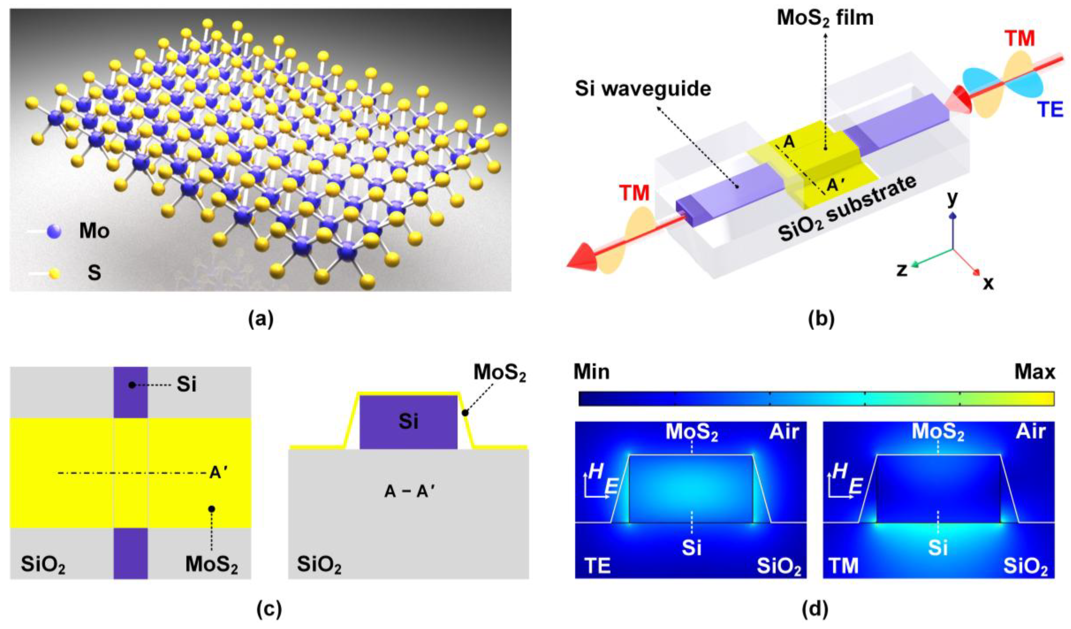
Figure 2.
(a) Schematic illustration showing the chemical vapor deposition (CVD) process flow we employed for synthesizing MoS2 monolayers. (b) Microscopic image of a monolayer MoS2 film coated on a sapphire substrate. (c) Atomic force microscopy (AFM) image of a MoS2 crystal synthesized by using the CVD method in (a). (d) Microscopic image of a MoS2-coated silicon-on-insulator (SOI) chip with opened windows.
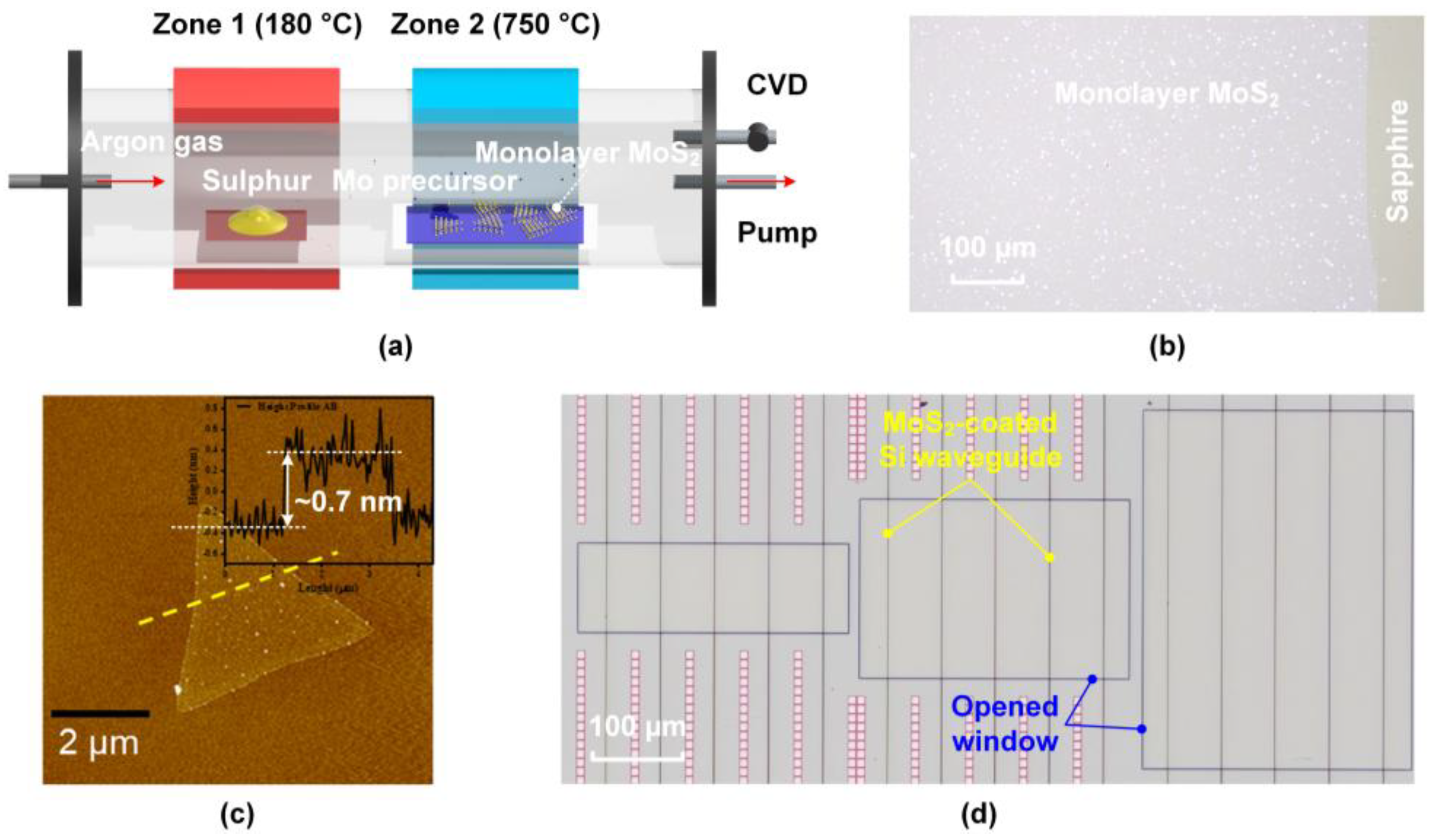
Figure 3.
Characterization of our synthesized monolayer MoS2 films. (a) Measured Raman spectra of an SOI chip (i) before and (ii) after coating a monolayer MoS2 film. (b) Ultraviolet–visible (UV–vis) absorption and transmittance spectra. (c) X-ray diffraction (XRD) spectrum. (d) X-ray photoelectron spectroscopy (XPS) spectra, where (i) and (ii) show characteristic peaks of Mo 3d and S 2p, respectively.
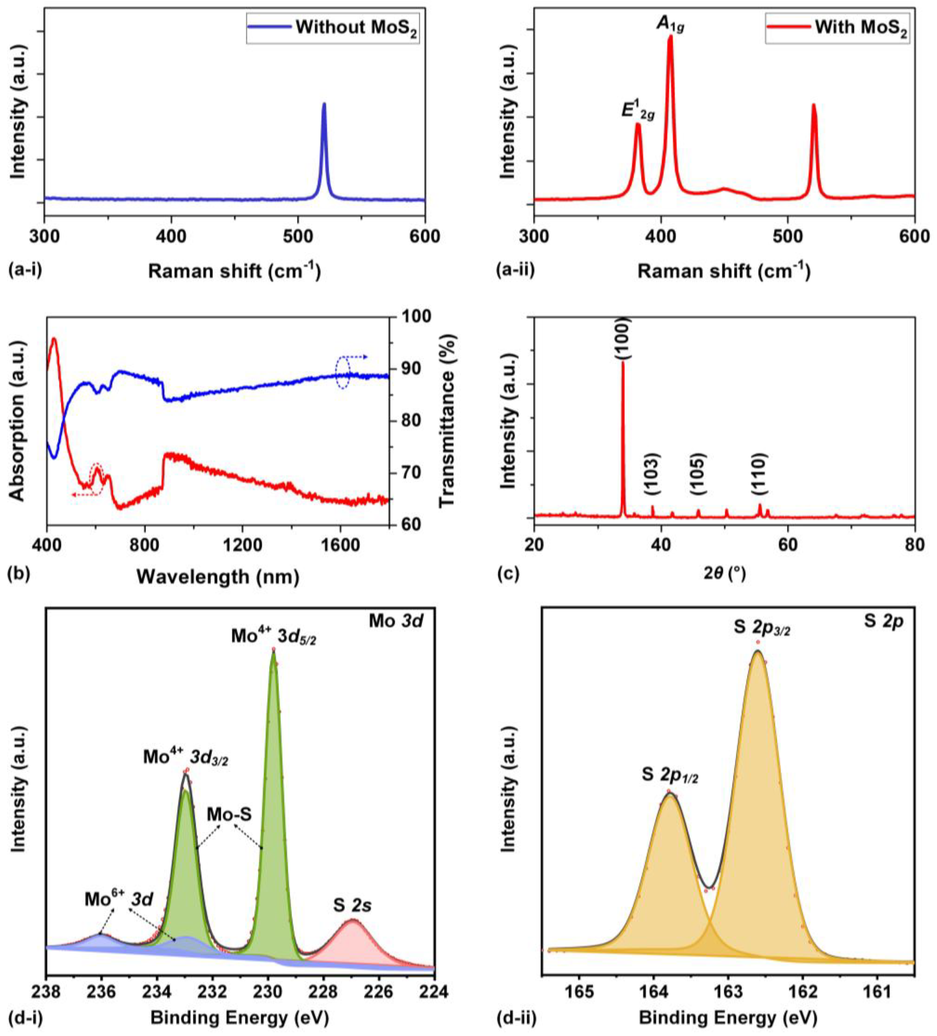
Figure 4.
(a) Measured IL versus MoS2 film coating length (Lc) for the MoS2-Si hybrid waveguides. (b) Measured insertion loss (IL) versus the waveguide width (W) for the MoS2-Si hybrid waveguides. In (a) and (b), (i) shows the measured results for TE & TM polarizations, and (ii) shows the polarization dependent loss (PDL) calculated from (i). (c) Polar diagrams for the measured IL of devices with (i) Lc = 1.0 mm and (ii) Lc = 2.2 mm. The polar angle represents the angle between the input polarization plane and the substrate. In (a-c), the input continuous-wave (CW) power and wavelength were Pin = ~0 dBm and λ = ~1550 nm, respectively. In (c), W = ~400 nm.
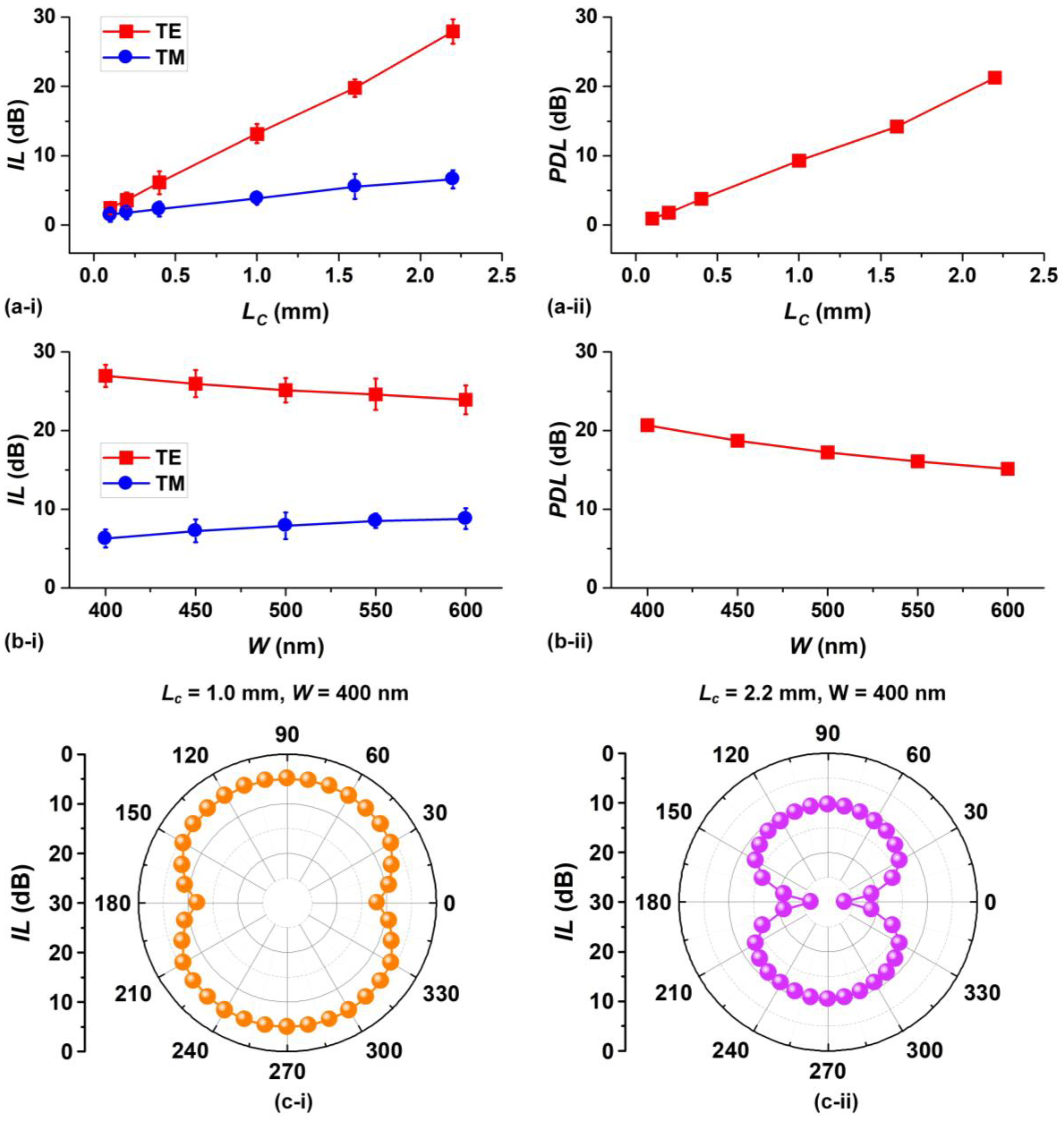
Figure 5.
(a) Measured PDL versus input CW wavelength λ for the MoS2-Si hybrid waveguides with different Lc but the same W of ~400 nm. (b) Measured PDL versus λ for the MoS2-Si hybrid waveguides with different W but the same Lc of ~2.2 mm. (c) ‒ (d) Measured TE- and TM-polarized IL and calculated PDL versus input power Pin for the MoS2-Si hybrid waveguides with Lc = ~1.0 mm and ~2.2 mm, respectively. In (a) and (b), Pin = ~0 dBm. In (c) and (d), the input CW wavelength and the waveguide width were λ = ~1550 nm and W = ~400 nm, respectively.
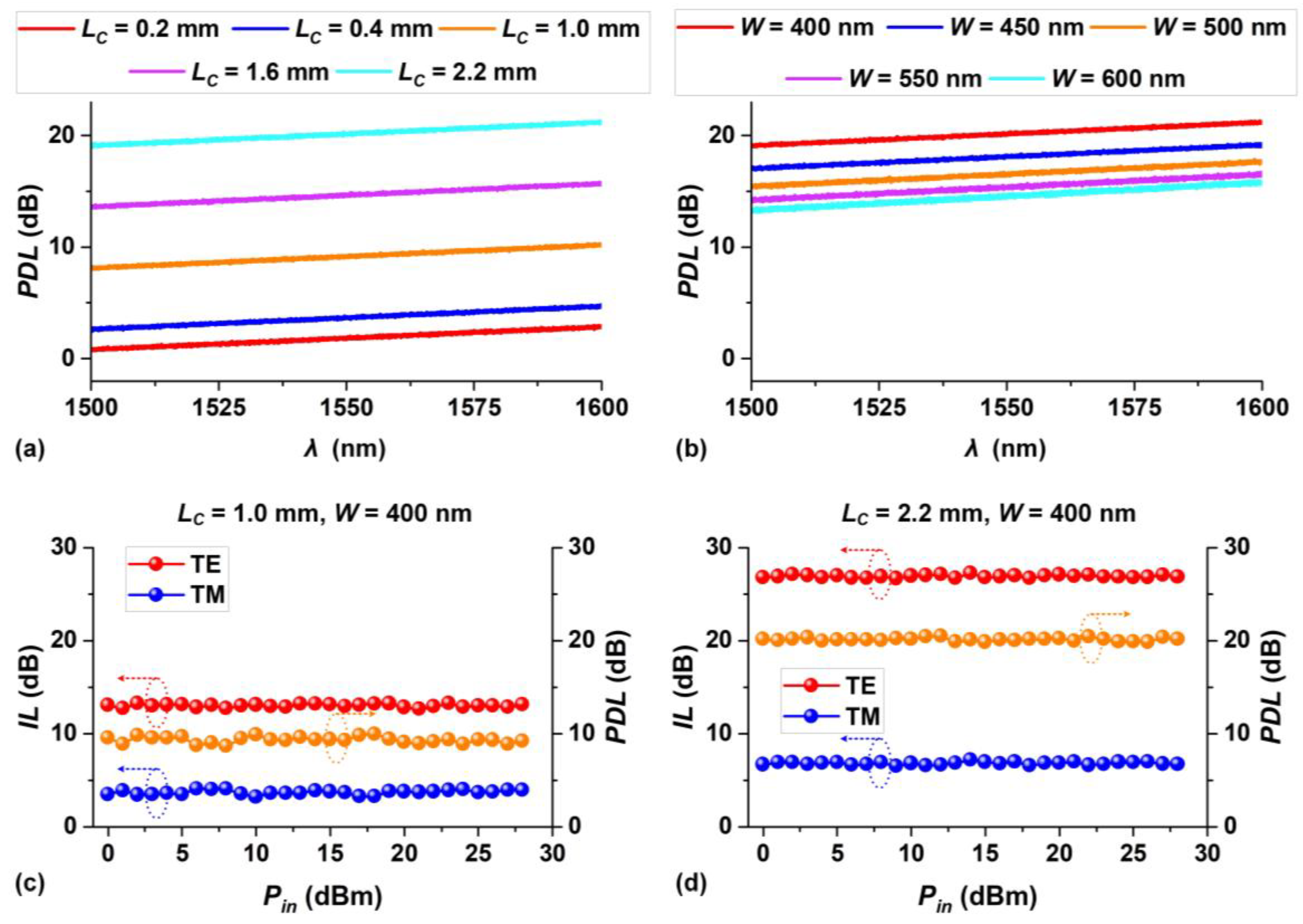
Figure 6.
(a) TE- and TM-polarized propagation loss (PL) versus silicon waveguide width W for the MoS2-Si hybrid waveguides. (b) TE- and TM-polarized extinction coefficients of MoS2 (kTE , kTM) versus W obtained by fitting the results in (a) with optical mode simulations. (c) Anisotropy ratio (kTE / kTM) calculated from (b). (d) Calculated figures of merit (FOM) versus W for the MoS2-Si hybrid waveguides.
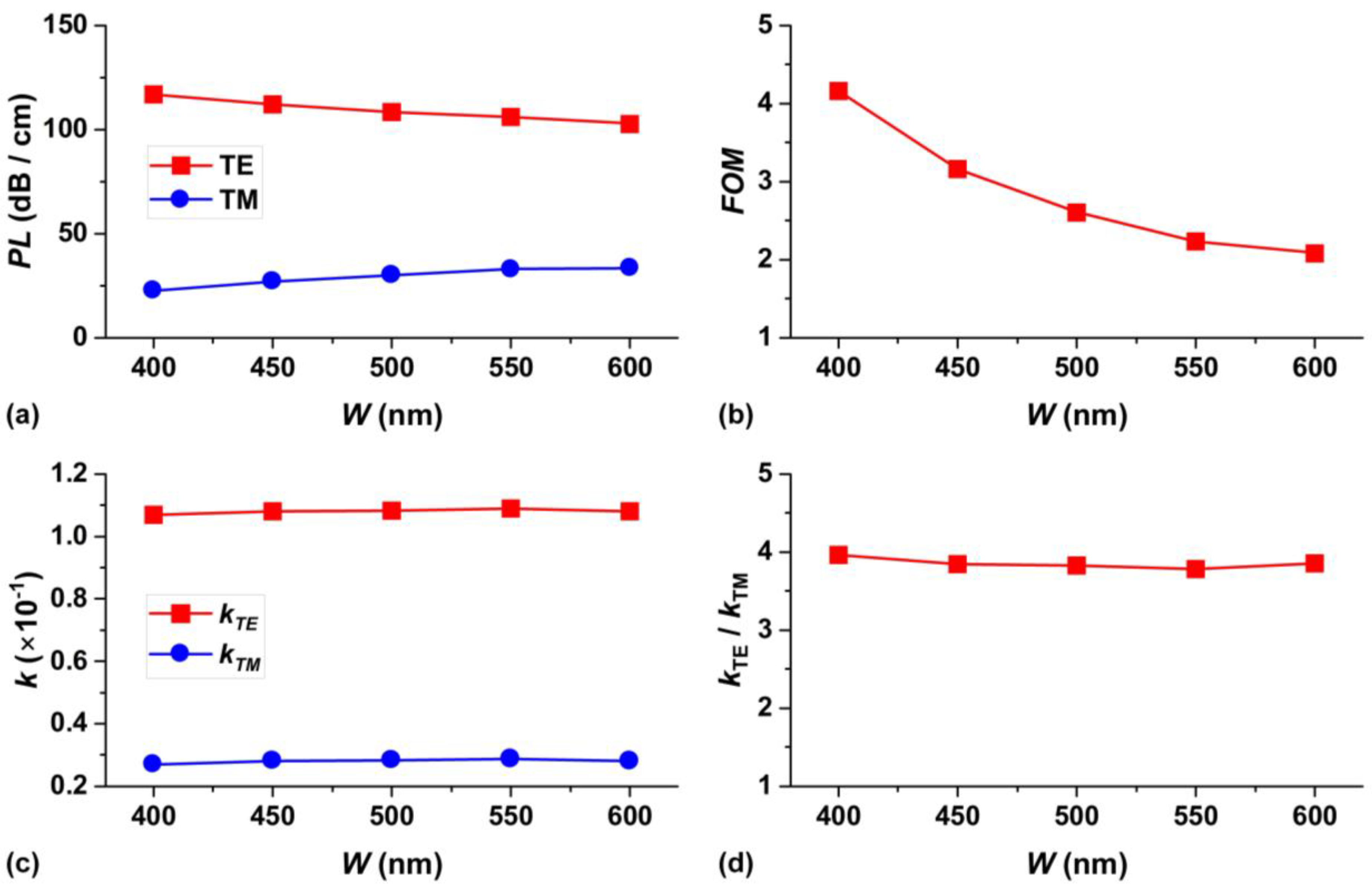

Table 1.
Comparison of waveguide optical polarizers incorporating 2D materials.
| 2D Material |
Waveguide Material | 2D Material Thickness | WD (µm) |
PDL (dB) |
OBW (µm) |
FOM | Ref. |
|---|---|---|---|---|---|---|---|
| Graphene | Polymer | ‒ a | 7.00 × 5.00 | ~19 | ‒ a | ~0.7 | [16] |
| Graphene | Glass | ‒ a | 11.50 × 2.60 | ~27 | ~1.23–1.61 | ~3.0 | [61] |
| Graphene | Chalcogenide | Monolayer | ‒ a | ~23 | ~0.94–1.60 | ~28.8 | [14] |
| Graphene | Polymer | > or < 10 nm b | 10.00 × 5.00 | ~6 | ‒ a | ~0.7 | [15] |
| MoS2 | Nd:YAG | ~6.5 nm | ‒ a | ~3 | ‒ a | ~7.5 | [21] |
| MoS2 | Polymer | ~2.5 nm | 8.00 × 8.00 | ~12.6 | ~0.65–0.98 | ‒ a | [22] |
| GO | Polymer | ~2000 nm | 10.00 × 5.00 | ~40 | ~1.53–1.63 | ~6.2 | [19] |
| GO | Doped silica | ~2–200 nm | 3.00 × 2.00 | ~54 | ~0.63–1.60 | ~7.2 | [17] |
| GO | Silicon | ~10 nm | 0.40 × 0.22 | ~17 | ~1.50–1.60 | ~1.7 | [18] |
| rGO | Silicon | Monolayer | 0.40 × 0.22 | ~47 | ~1.50–1.60 | ~3.0 | [62] |
| MoS2 | Silicon | Monolayer | 0.40 × 0.22 | ~21 | ~1.50–1.60 | ~4.2 | This work |
WD: waveguide dimension, PDL: polarization dependent loss, OBW: operational bandwidth, IL: insertion loss, FOM: figure of merit. aThere is no reported value for this parameter in the literature. bThe polymer waveguides with a few-layer graphene film (< 10 nm) and a thicker graphene film (> 10 nm) worked as TM- and TE-pass optical polarizers, respectively.
Disclaimer/Publisher’s Note: The statements, opinions and data contained in all publications are solely those of the individual author(s) and contributor(s) and not of MDPI and/or the editor(s). MDPI and/or the editor(s) disclaim responsibility for any injury to people or property resulting from any ideas, methods, instructions or products referred to in the content. |
© 2025 by the authors. Licensee MDPI, Basel, Switzerland. This article is an open access article distributed under the terms and conditions of the Creative Commons Attribution (CC BY) license (http://creativecommons.org/licenses/by/4.0/).
Copyright: This open access article is published under a Creative Commons CC BY 4.0 license, which permit the free download, distribution, and reuse, provided that the author and preprint are cited in any reuse.


