
Submitted:
20 May 2025
Posted:
22 May 2025
You are already at the latest version
Abstract
The topic of forces on a dielectric slab between the two conductors of a parallel-plate capacitor is a classic textbook example that has drawn repeated attention of physicists for pedagogical reasons and beyond. It is pointed out in this paper that the critical role of Newton’s third law was not fully exposited in the current literature. This omission led to the current view that the force on the slab is solely due to the fringing field near the edges of a capacitor and, yet we can correctly compute the force while neglecting the fringing field. Considering the third law explicitly, multiple views are shown to be equally valid about where the forces are distributed. In a straightforward view presented in this paper, the force on the slab by the capacitor is mostly distributed deep inside the capacitor, more than near the edges. The textbook formula for the force is the zeroth-order approximation in terms of the fringing field. The inclusion of the fringing field will add correctional terms to the formula.
Keywords:
electric field
; Newton's third law
I. Introduction
Computing the force on the dielectric slab in a parallel-plate capacitor (illustrated in Fig. 1) is a textbook problem loved by teachers and students of physics[1,2,3,4,5,6,7,8]. The most popular way of computing this force is to consider the energy of the system as a function of the dielectric’s position (), , where is the charge in the capacitor and is the capacitance. The force is given by , suggesting that the forces on the slab act on the top side of the slab (). It was put forward in Refs.[5,8], however, that the forces are all due to the fringing fields near the edge of the capacitor. The energy-variational method gives the correct result for the force even while totally ignoring the fringing fields that are solely responsible for the force[5,8]. The objectives of this paper are:
1. Pointing out that Newton’s 3rd law was implicitly used in the current literature, causing mix-ups in the force distribution; The forces on the dielectric computed as aforementioned are by the total electric field , mixing together the forces by the charges on the parallel plates and the internal forces among the induced charges. By Newton’s 3rd law, all the internal forces among the induced bound charges sum up to be zero. Consequently, the total force by the total electric field is equal to the total force by the external electric field . However, the distribution of the forces by the total electric field differs from the distribution of the external forces on the dielectric by the external electric field , excluding the internal electric field produced by the induced bound charges (polarization). It is fundamental and pedagogically beneficial to distinguish these two distributions. By a different energy-variational method and by a brute-force method, the forces by the external electric field can be shown to be distributed all over the slab rather than solely by the fringing fields.
2. Presenting a different energy-variational method (Section II);
3. Presenting a brute-force computation to illustrate the distribution of the external forces on the dielectric slab (Section III).
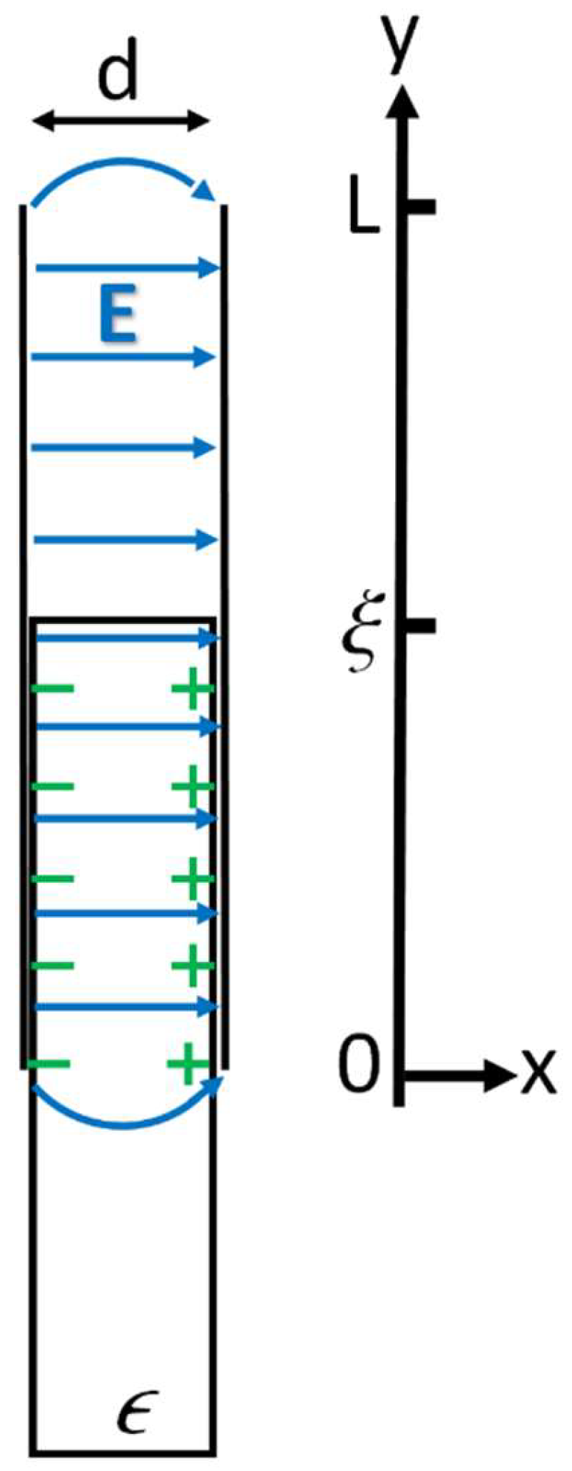
Figure 1.
A dielectric slab partly inside a parallel-plate capacitor. The coordinates are chosen as x-axis being perpendicular to the plates, y- (vertical) and z- (pointing out of the page) axes being parallel to the plates. The two plates are LL in dimensions, separated by a distance d. x indicates where the dielectric slab is inside the capacitor. . The total/net electric field E is illustrated as blue arrows, which is uniform inside the capacitor and nonuniform near the edges of the plates (fringing fields). The green colored + and – signs indicate the bound/induced charges on the surfaces of the dielectric slab. The free charges on the conductor surfaces are not shown here (they will be explicitly illustrated in Fig. 3).
II. A general energy-variational method
In fact, an exact energy method can be readily derived for the force on a dielectric piece by two charged conductors whether they are disconnected or remain connected to a battery (illustrated in Fig. 2). The energy cost to the system of the two conductors and the battery for bringing the presence of the dielectric is[4]
Here and are respectively the energy of the system in the presence and in the absence of the dielectric. The first term on right hand side of Eq. (1) represents the energy cost to the battery which is zero if the switch is open but nonzero if the switch is closed. is the electric field in the absence of the dielectric and , the corresponding displacement field. is the electric field all over the space in the presence of the dielectric while inside the dielectric and outside it. The volume integrations are all over the space outside the two conductors.
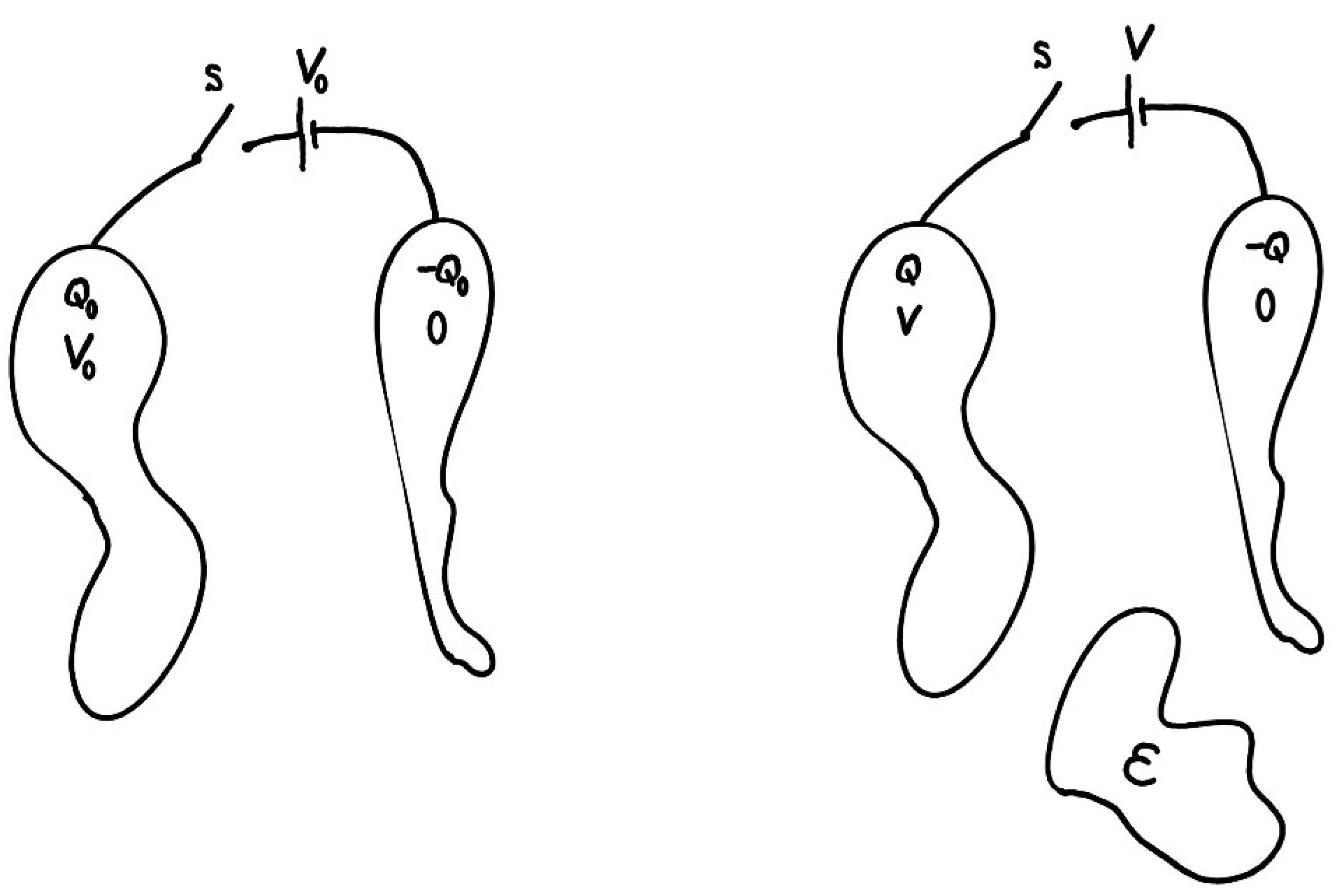
Figure 2.
In the left, two conductors fully charged by a battery of voltage . The conductor connected to the positive pole of battery rests at a potential and carries a total charge of while the conductor connected to the negative pole of battery remains at potential zero and carries a total charge of . In the right, a piece of dielectric material (marked ) is placed into the two-conductor system. The introduction of the dielectric piece causes changes to the charges or the potentials of the two conductors, depending on the switch S being closed ( and ) or open ( and ).
Rearrange the terms, the formula becomes the following[4]:
Note that the static electric fields are gradients of the scalar potential fields and . The first integral of Eq. (2) can be manipulated as follows:
where first volume integral becomes a surface integral on the surfaces of the two conductors while the second volume integral vanishes because there are no free charges in the space outside the conductors, . Consequently,
Here, is equal to the free charge density on the conductor surface in the presence of the dielectric while is equal to the surface charge density in the absence of the dielectric. The second integral of Eq. (2)
Put them altogether, one can obtain the following result:
when the first term becomes zero whether switch is closed () or open (). is the polarization of the dielectric. The integration is over the volume of the dielectric. It is worth noting that the integrand involves the dot product of the electric fields and . These two fields may not align exactly the same directions everywhere but their dot product is positive inside and outside the dielectric. Therefore, the interaction between the dielectric and the two-conductor system is attractive in nature. The total force is toward where the electric field is stronger. Considering an infinitesimal whole-body displacement of the dielectric, , the corresponding change in energy gives the following formula for the force on the dielectric:
Here the first integration is over the entire surface of the dielectric and the unit vector is the normal vector of the surface (pointing out of the dielectric volume) while the second integration is inside the volume of the dielectric object, of course. represents derivative of the electric field with respect to the infinitesimal displacement of the dielectric, which vanishes if the switch is closed. Applying this formula for the problem of a parallel-plate capacitor shown in Fig. 1, the integration can be expressed as the sum of four surface integrals on the top, the bottom, the left-side, and the right-side surfaces of the rectangular dielectric slab. On the left and the right surfaces, is symmetrical (deep inside the capacitor or near the edges) but the two sides have oppositely directed normal vectors. Therefore, the two integrals on the left and the right sides cancel out. On the bottom, the fields are negligible under the small-fringing field approximation when . Likewise, the front and the back sides are not even considered here. The integral on the top surface gives the total force pointing along the y-direction, which is identical to the current literature.
III. Brute-force method for force by the external field
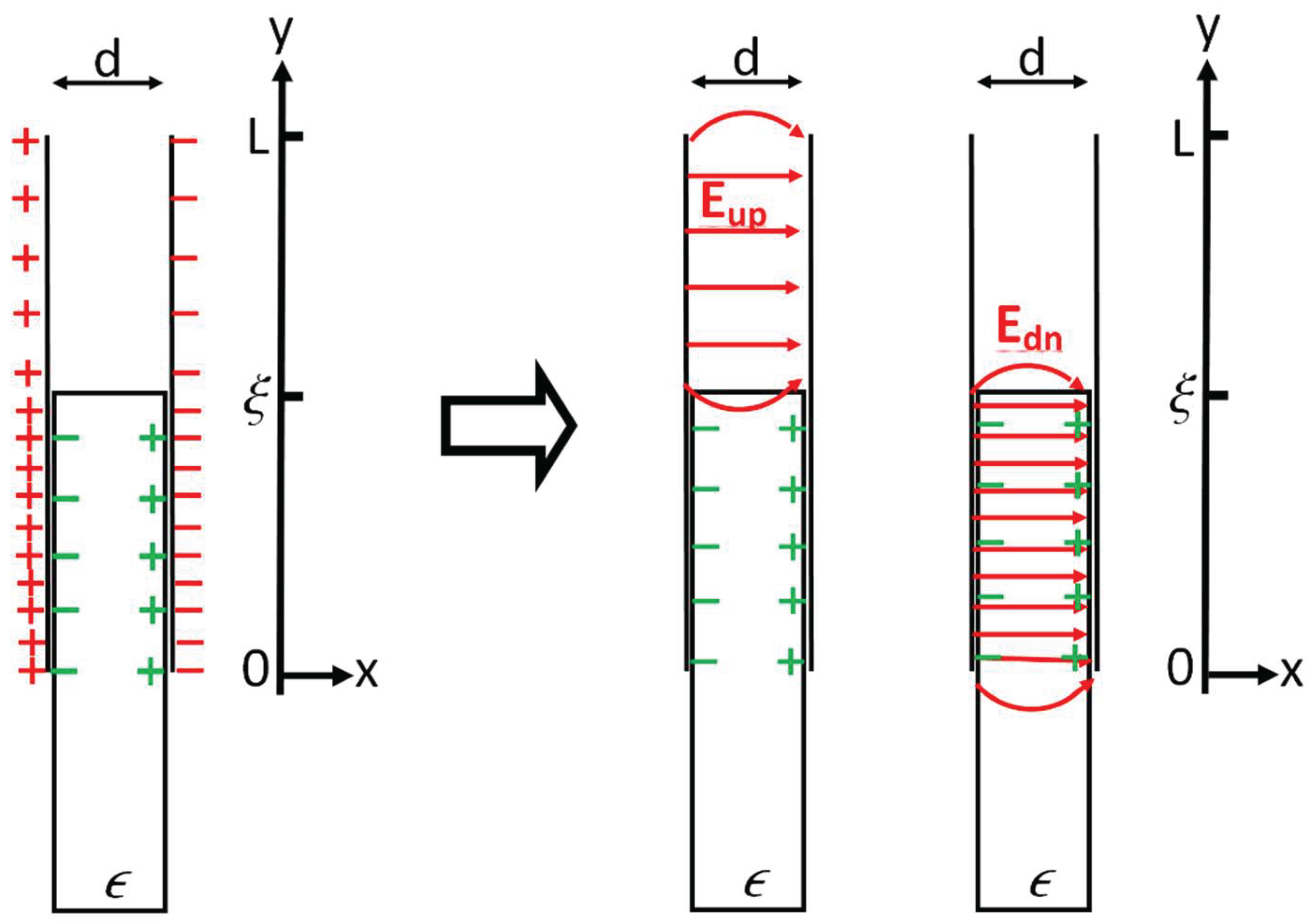
Now the straightforward consideration of the external forces on the dielectric by the charges on the plates without the complication of the internal interactions. This consideration is illustrated in Fig. 3. The charges on the upper parts of the plates ( produce the electric field and the charges on the lower parts of the plates produce the electric field . In the approximation for , in the zeroth order of , is approximately equal to that of a uniform surface charge on the semi-infinite plane ( located at and the same of on the semi-infinite plane located at :
where and are the unit vectors along the x- and y-directions respectively. is approximately equal to that of a uniform surface charge on the infinitely-long rectangular plane ( located at and the same of on the plane located at :
Naturally, is the external electric field produced by the charges on the capacitor plates, excluding the electric field given by the induced polarization . Clearly, is not uniform inside the capacitor even when the fringing fields are ignored. So is or . Noting that is stronger than by a factor of . The forces on the induced bound charges by the external field is distributed all over the dielectric (wherever is not uniform), including deep inside the capacitor and near the edges. Interestingly, the total force on the dielectric can be expressed as the 3D integral inside the entire volume of the dielectric that is exactly equal to the 2D integral over the surface of the slab (per Gaussian theorem):
Here is the 3D density of the induced bound charge inside the volume of the dielectric which is equal to zero because there is no free charge embedded inside the dielectric. is the 2D density of induced bound charge on the surface of the dielectric. On the right-side surface of the dielectric, and, on the left-side, while on all the other sides. It is emphasized that the external field is nonuniform deep inside the capacitor and near the fringes. Using the volume integral or using the surface integral, the forces by the external field on the dielectric are distributed both inside the capacitor and near the fringes. Using the surface integral of Eq. (10) with ,
Note that the lower field is mostly along the x-direction (Fig. 3), responsible for polarizing the dielectric. The forces by on the bound charges on the left-side and the right-side surfaces of the slab are symmetrical to cancel each other. In contrast, the forces by on the bound charges are mostly upward to sum up to the total force. Specifically, plugging Eqs. (8) and (9) into Eq. (11), the x-components cancel out while the y-components give rise to two exactly integrated integrals:
which is the well-known result from other methods. Here, the terms on the orders of or are neglected. They are the true fringing-field terms. In this brute force computation, the force on the dielectric is again shown to be not solely due to the fringing field near the edge of the capacitor. Its actions are mostly deep inside the capacitor instead. Furthermore, taking account of the fringing fields will alter the computed force with additional terms on the orders of or that are ignored in the current literature as well as in this paper.
IV. Conclusions
In conclusion, it is fundamentally and pedagogically interesting to pin down the distribution of the force on the dielectric slab by a parallel-plate capacitor. Getting to the bottom of this classic textbook example, students will better appreciate the beauty and power of physics in simplicity and complexity.
Acknowledgements and declarations
The author declares that no conflict of interest exists.
References
- S. Margulies, American Journal of Physics 52 (6), 515-518 (1984).
- C. A. Utreras-Díaz, American Journal of Physics 56 (8), 700-701 (1988).
- J. J. Meyer and A. F. Behof, American Journal of Physics 62 (10), 931-934 (1994).
- J. D. Jackson, Classical Electrodynamics, 3rd ed. . (John Wiley & Sons, Inc., Hoboken, N.J., 1998).
- E. R. Dietz, American Journal of Physics 72 (12), 1499-1500 (2004).
- T. T. Grove, M. F. Masters and R. E. Miers, American Journal of Physics 73 (1), 52-56 (2005).
- L. P. Staunton, American Journal of Physics 82 (9), 853-859 (2014).
- D. J. Griffiths, Introduction to Electrodynamics, 4th ed. . (Cambridge University Press, New York, N.Y., 2017).
Figure 3.
Explicit show of charge distributions and external electric field that is not uniform inside the capacitor. On the left, the red colored + and – signs indicate free/external charges on the plates while the green colored ones indicate the induced charges on the surface of the dielectric slab. On the right, the free charges are not shown. The external electric field is split into two parts: The field is produced by the free charges on the upper part of the plates where the dielectric slab is absent and the field is produced by the free charges on the lower part of the plates when the dielectric slab is present.
Disclaimer/Publisher’s Note: The statements, opinions and data contained in all publications are solely those of the individual author(s) and contributor(s) and not of MDPI and/or the editor(s). MDPI and/or the editor(s) disclaim responsibility for any injury to people or property resulting from any ideas, methods, instructions or products referred to in the content. |
© 2025 by the authors. Licensee MDPI, Basel, Switzerland. This article is an open access article distributed under the terms and conditions of the Creative Commons Attribution (CC BY) license (http://creativecommons.org/licenses/by/4.0/).
Copyright: This open access article is published under a Creative Commons CC BY 4.0 license, which permit the free download, distribution, and reuse, provided that the author and preprint are cited in any reuse.


