Submitted:
04 February 2026
Posted:
05 February 2026
You are already at the latest version
Abstract
In this work, we investigate n-channel Si MOSFETs commonly used in radia-tion-hardened electronics for space and nuclear applications. Radiation-induced defects degrade the transistor electrical characteristics, particularly the current–voltage behavior. Experimental results reveal a negative shift in the threshold voltage with increasing gamma-ray doses up to 348 krad, mainly attributed to the trapping of positive charges in the gate oxide. In the proposed model, these trapped charges are represented through an effective acceptor concentration NAeff, introduced as a phenomenological parameter to describe their electrostatic influence on the inversion layer, without implying any physical modification of the silicon doping. Static (DC) and small-signal (AC) current models are developed to describe the post-irradiation electrical behavior. Empirical relationships linking device parameters to the total ionizing dose are extracted from experimental I–V measurements. The proposed approach provides a compact framework suitable for low-frequency circuit-level simulations under radiation environments.
Keywords:
SOI n-MOSFET
; gamma radiations
; I-V characteristics
; total ionizing dose
; in-situ thermal annealing
; electron traps
I. Introduction and Related Works
During the last decades, significant progress has been achieved in epitaxial growth and technological design for both bipolar-junction and metal-oxide semiconductor FETs [1,2,3,4]. The challenge has been how to reduce the detrimentaleffects of imperfections. However, impurities and defects are always present in the host lattices, thus inducing localized extrinsic states in the active layers. Most process-induced traps behave as trapping centers, leading to deposited positive charges. The origin of these active traps, and especially their locations, has been characterized using various techniques, but explanations remain controversial. It is worth noting that defects may be intrinsic or arise from extrinsic origins.
For MOSFET transistors operating in hostile environments, exposure to gamma radiation can cause significant disturbances in their characteristics and functionality [5,6,7].The dose rate of gamma radiation is an important parameter influencing the degradation mechanisms in MOSFETs, as highlighted in previous studies [8,9,10]. In thiswork, as ample of 1µm SOI-PD nMOSFETs from xfab, were irradiated using a Co-60 gamma source with a controlled dose rate of 1.2 krad(Si)/h. The total ionizing dose (TID) applied was up to 348 Krad. The chip were packaged in a Dual-In-Line ceramic package and connected to a load board for bias application and I-V measurements during Irradiation.
The investigated devices are commercial n-channel silicon MOSFETs fabricated using a conventional CMOS process on p-type substrates. Gamma irradiation experiments were carried out at room temperature using a calibrated Co-60 source. The total ionizing dose (TID) was progressively increased up to 348 krad(SiO2) under unbiased conditions. After irradiation, the devices were subjected to a thermal annealing step performed in ambient atmosphere at 120°C for 30 minutes. Electrical I–V measurements were performed before irradiation, after irradiation, and after annealing. Measurements were conducted on multiple nominally identical devices for each dose level. The reported results correspond to average values, showing good reproducibility and limited dispersion. The TID induce permanent and cumulative degradation of the transistor's electrical properties during gamma radiation. These degradations are mainly attributed to an accumulation of trapped holes in the oxide layer and at the oxide–channel interface [11]. It is important to mention that the density of trapped charges strongly depends on device architecture and the technological process [12].As a first approach to mitigate trapped charge effects, irradiated transistors were subjected to annealing at relatively high temperatures over prolonged heating periods [13,14]. However, the major drawback of this procedure is the high thermal energy consumption. In recent works, advanced recovery methods have been developed using micro-integrated hot plates, which offer rapid response, low power consumption, and in-situ electro-thermal annealing [13,15].From a technological perspective, it has also been demonstrated that the immunity to transient gamma radiation effects can been hanced by including buried-oxide (BOX) epilayers [12], which separate the thin silicon active layer from the substrate. This novel technique has proven successful in partially or completely recovering degradation over a wide range of TIDs [16,17].
The understanding of radiation-induced defect dynamics has been expanded through recent studies, highlighting the role of interface states and oxide traps on device degradation mechanisms [18,19]. Moreover, the dose rate and energy spectrum of the gamma source critically influence the extent of degradation, as shown in various experimental investigations [20.21]. The aim of the present to investigate the effects of gamma radiation on electron transport in a Si-based n-MOSFET with a 1 µm channel length. I-V output measurements were performed before and after thermal annealing. From these I-V characteristics, we extracted threshold voltage, transconductance, and conductance parameters.
This work focuses on compact and phenomenological modeling for post-irradiation electrical characterization and circuit-level analysis. It does not aim to introduce new fundamental radiation damage mechanisms nor to propose RF-validated transistor models. The modeling framework is intentionally based on classical MOSFET analytical formulations, with radiation effects incorporated through effective electrostatic parameters. In particular, the effective acceptor concentration NAeff introduced in this study does not represent a physical modification of the silicon doping profile. It is defined as a phenomenological parameter that captures the electrostatic influence of radiation-induced oxide and interface trapped charges on the channel potential. This approach enables the integration of total ionizing dose effects into standard MOSFET models while preserving intrinsic material and technological parameters.
The paper is organized as follows: after this introduction, section II presents the DC and small-signal models, section III discusses the results, and section IV summarizes the conclusions.
II. DC and Small-Signal Models for an n-MOSFET
This section recalls only the minimum set of standard MOSFET expressions required to interpret the experimental results. Textbook-level derivations are omitted for brevity. Radiation effects are introduced through effective electrostatic parameters that capture the influence of oxide- and interface-trapped charges.
II.1.The Direct-Current Model
In the proposed modeling approach, radiation effects are incorporated through effective electrostatic parameters. In particular, the parameter NAeff is introduced to phenomenologically capture the electrostatic impact of oxide- and interface-trapped charges on the inversion layer. This parameter should not be interpreted as a real change in substrate doping.
Assuming a quasi-static transport regime and a constant carrier mobility along the channel, the local drain current density at a position y can be written as:
where QN(y) is the local inversion charge density per unit area.The drain–source current IDS is a global quantity and is obtained by integrating the local current density along the entire channel length:
By changing the integration variable from y to the channel potential V, the expression becomes:
Although the local current density is expressed as a function of the channel position y, the drain current IDS is obtained after integration along the full channel length and is therefore independent of y.
The inversion charge density is expressed as:
where, is the Fermi potential , and d is the gate oxide thickness. The effective acceptor concentration NAeff captures the effect of oxide-trapped charges.
From IDS, the key DC parameters are derived :
Transconductance:
Conductance
II.2. Drain Current in Linear and Saturation Regimes
II.2.1. Linear Regime
For and , the drain current reduces to:
with is the oxide capacitance per unit area
and is the threshold voltage
In this regime, the drain current varies linearly with VDS and VGS (for VGS>Vth). The transconductance and conductance are given by:
As can also be noticed from Eq. (4), bothand show a linear variation as a function of the VDS and VGS bias potentials.
II.2.2 Saturation regime-Effect of the channel modulation
When VDS exceeds the linear regime, the electron density QN(y) decreases near the drain, and the current tends toward saturation. Saturation occurs when the channel pinch reaches the drain:
and .
For a VDS supper than VDS,SATthe excess voltage - drops across a depleted region of width ΔL, and the channel conductance increases:
As revealed from Eq.6, the IDS−VDS characteristics of an n-MOSFET exhibit an increase with VDS, thus affecting the parameters gm and gd.
II.3. Small-Signal Model
II-3-1 Resistive Operating
In the linear regime, the n-MOSFET behaves as a resistance controlled by VGS
In technological applications, the n-MOSFET in linear regime can be used as an on-off switch.
II-3-2 Operation as an amplifier
In saturation, the n-MOSFET behaves as an ideal current sour
Channel modulation for VDS > VDS,SAT is described by Eq.6. The output resistance is:
The parallel combination of I0 and _Ro forms the low-frequency small-signal equivalent. At higher frequencies, capacitances must be included as in Figure 1.
The small-signal hybrid parameters are:
The small-signal hybrid parameters are:
For h22RL<<1, simplified formulas are:
The cut off frequency is:
III. Static and Dynamic Characteristics of an Irradiated n-MOSFET
III-1 Static Parameters
The n-MOSFET under investigation was fabricated using a 1 µm partially depleted SOI technology. The device is implemented within a 600 µm-diameter circular membrane located near an integrated micro-heater used for in-situ thermal annealing. Two auxiliary PIN diodes are placed on the membrane to monitor the temperature during operation. A detailed description of the fabrication process and the annealing procedure is available in Ref. [12]. Electrical characterization was carried out by measuring the drain current as a function of the gate-to-source voltageVGS in both linear and saturation regimes, with the drain-to-source voltage VDS fixed at 50 mV and 3 V, respectively. Measurements were performed before and after gamma irradiation. The gate dielectric of the investigated n-MOSFET consists of a 25 nm-thick thermally grown silicon dioxide (SiO2) layer formed by dry thermal oxidation. The quality of this gate oxide, including its defect density and interface trap concentration, plays a critical role in the device response to gamma radiation exposure. Radiation-induced degradation primarily results from charge trapping within the oxide and from interface state generation at the Si–SiO2 interface. Consequently, the parameters employed in the proposed modeling approach, such as the effective trapped charge density and equivalent doping variations, are directly related to these gate oxide properties and the fabrication technology.
Gamma irradiation experiments were performed at room temperature using a calibrated Co-60 source with a dose rate of 1.2 krad(Si)/h. The total ionizing dose was increased up to 348 krad(Si). Electrical measurements were conducted on several nominally identical devices in order to assess reproducibility. All devices exhibited consistent trends with limited sample-to-sample dispersion, and the results presented in this work correspond to averaged values representative of the technology. After irradiation, thermal annealing was performed at 120 °C for 30 minutes in ambient atmosphere using the integrated micro-heater.
The threshold voltage Vth was extracted using the conventional subthreshold extrapolation method. The drain current IDS was plotted on a logarithmic scale as a function of the gate voltage VGS , and a linear fit was performed in the subthreshold region, where the current exhibits an exponential dependence on VGS. The threshold voltage was determined from the intersection of the extrapolated linear fit with the reference threshold current. This extraction procedure, illustrated in Figure 2, follows the methodology reported in Applied Physics Letters 48, 133–135 (1986).
The same extracted Vth values are consistently used in the determination Qox-eff and NAeff in order to avoid any artificial trend inversion and to ensure physical consistency.
Figure 3.
a. The threshold-voltage as a function of Figure3 b. Cross-Sectional schematic of n-MOSFET.
Figure 3.
a. The threshold-voltage as a function of Figure3 b. Cross-Sectional schematic of n-MOSFET.
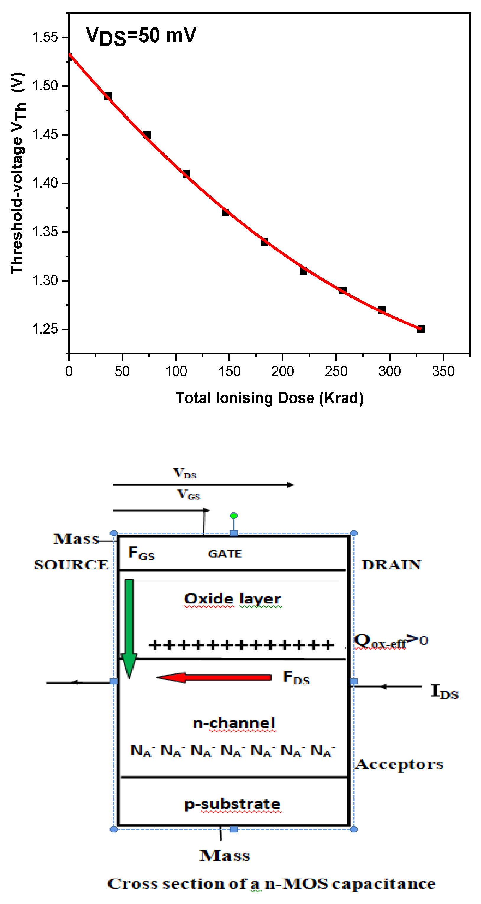
The total Ionizing Dose in the linear regime structure showing the oxide layer, trapped oxide charges, and the effective acceptor concentration in the channel region of a n-MOS capacitance
It clearly appears that the threshold-potentialshows a decreasing tendency as TID increases. Using a linear fit, the threshold potential Vth(TID) reads in the linear-regime as:
As reported in Ref.[12], the threshold voltage shift is expectedto result from a trapping of positive charges inside the oxide layer and at oxide n-channel. Let be the total density of oxide-and interface-trapped holes per unit area, is related to Qox-effusing the model (12):
Qox-eff represents a charge density per unit area and is therefore expressed in C/cm2
With From Vth=Vth(TID), we have deduced the interfacial gate-oxide density Qox-eFF versus TID. Obtained results are shown in Figure 4.
As it is found, Qox-eff shows an amount with increased gamma radiation dose. In terms of an analytical fitting, its expression is as follows:
As an illustrative picture, we report in theFigure 3.b the cross section of the MOS capacitance for a n-MOSFET under bias potentials VGS and VDS. The inset clearly shows the deposited interfacial holes under the effect of FGS electric field. On the other hand, radiation hardening technologies reveal that thin gate oxide designs have a large capacitance which leads to a reduced threshold voltage shift. In terms of quantum tunneling, thin gate-oxide transistors favour the recombination of trapped holes with electrons initially located in the channel [22,23]. This can efficiently help MOSFET devices with thin gate-oxide thicknesses to become more hardened against hostile radiating environments. From the inset of Figure 3, it is seen that the n-channel is located between ionized acceptors in Si-substrate and trapped holes. Physically, this implies that free electrons in the conductive channel are jointly subjected to a double electrostatic interaction. In terms of equilibrium charge balance, acceptors can be considered as partially compensated by equivalent donor centers. This leads to define an effective density of the doped acceptors as where represents the centesimal percent of compensation. According to this relation, the threshold voltage shift can be expressed as a function of NAeff. using the new model:
with
In establishing this relation, we have assumed that K does not vary significantly with TID. For the parameters NA, ni and Cox, we have taken the corresponding values 1.171017cm-3, 1,51010 cm-3and 1.3810-3 Fm-2 respectively. From the measurements of Vth versus TID in the linear regime, we have deduced NAeff. and results are summarized in Figure 5. As clearly shown, NAeff. (cm-3) exhibits a decreasing trend as the gamma radiation dose increases. Analytically, the effective doping concentration of acceptors is fitted by a quadratic law according to:
So that, the choice of NAeff seems to being physically meaningful as Qox-eff to analyze the electron transport in an irradiated n-MOSFET. From measurements in the linear regime, we have also extracted the transconductance. The relevant results are depicted in Figure 5.
Two peculiar features were revealed:(i) For a fixe VGS the transconductance decreases with increased TID, (ii) Under a gamma radiation dose, the transconductance decreases as the gate-to-source voltage increases. On the other hand, the transconductance can be fitted by the TID-dependent expression:
In the saturation regime, however, measurements of the drain current have been carried out as follows. Figure 6 depicts the relevant IDS versus TID for different applied VGS ranging from 1V to 3V.
The drain is subjected to a fixed bias voltage VDS=3V. The plots reveal that:(i) for a VGS lower than 1.5V which corresponds to the threshold potential, the drain current does not show a significant change as the TID varies, (ii) Beyond this value, I-V at output exhibits, in contrary, an increasing tendency as TID increases. As it is also noted, the increasing of IDS is more noticeable with increased VGS. Similarly to IDS in the linear regime, saturated I-V characteristics are found to be fitted as a function of TID by a polynomial law with VGS-dependent coefficients.
An attempt to explain the latter results will be subsequently proposed. The first feature is predictable since the conductive channel is not yet formed below the threshold potential. While the increase in IDS as observed for VGS greater than Vth is due presumably to the flow of an excess of free electrons originating from hole-electron pairs created at the vicinity of the channel in Si-substrate, In n-MOSFET transistors exposed to high TIDs, it is worth noting that this dysfunction can lead to a derivation of the operating point. From I-V measurements performed in the saturation regime, we have deduced as well the transconductance versus TID and VGS, see Figure 7.
As a main observation, the transconductance shows an increasing trend with increased TID. From a polynomial fitting, it was found that the transconductance can be written under the form:
The latter static parameter to being deduced is the conductance. As an experimental support, the drain current IDS has been measured versus VDS only for TID=0 Krad and TID=348 Krad. The gate voltage is fixed at VGS =3V. From the relevant I-V characteristics, we have determined the conductance versus VDS. . Results are shown in Figure 8.
It is thus found that the conductance shows a large amount with respect to that at TID=0 Krad for VGS inferior to 2 V, which corresponds to VDS,SAT. In the saturation regime, however, the conductance does not exhibit a significant change under the impact of gamma radiations. Note that, in the absence of experimental data for intermediate TIDs, it has not been possible to achieve a direct fitting. But the TID-dependence of this parameter can be derived from the transconductance by using the relationships
The threshold-potential VTh and the transconductance in both regimes gmLR and gmSR have been calculated as a function of TID above.
III-2 Hybrid and Dynamic Parameters
A deal of interest has also been paid to the dynamic characteristics under the impact of gamma radiations. In section II, the hybrid parameters of the non- irradiated n MOSFET are defined by Eq. (10). As it is seen, they are related to the transconductance gm, the total capacitance C and the resistance RO at output. Note that these static parameters are affected by the TID. From Eq. (10), we can deduce the modulasof the hybrid parameters as a function of TID.
The TID-dependence of the dynamic parameters can be established as well using the set of relations:
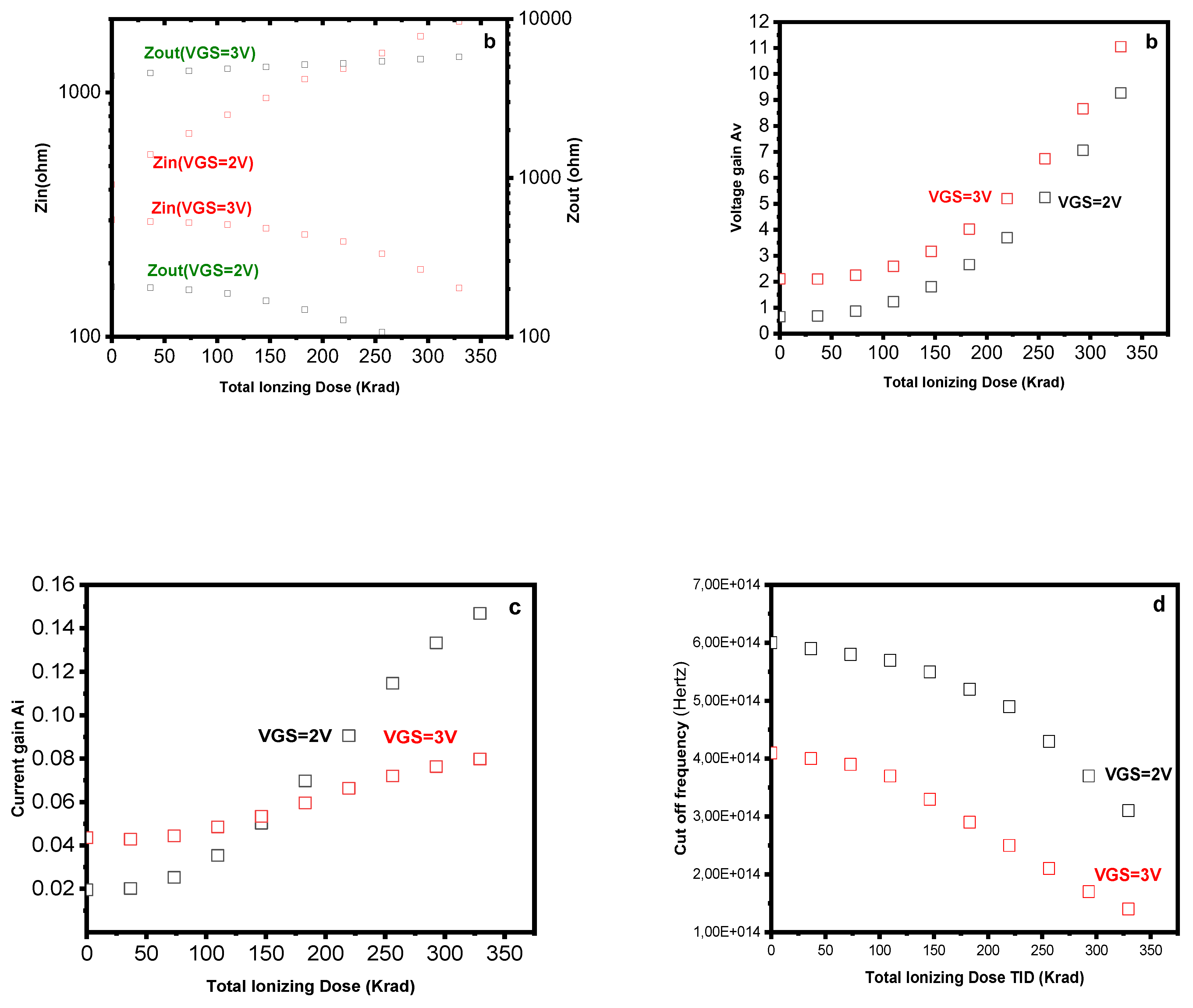
The small-signal model developed in this work is purely analytical and derived from the static I–V characteristics under quasi-static, low-frequency assumptions. Its purpose is to analyze qualitatively the evolution of AC parameters as a function of total ionizing dose. This model is not intended for RF or high-frequency operation, and all previous references to unrealistic frequencies have been removed. The gate-to-source voltage VGS is treated as an adjustable variable. Using Eqs (24) and (25), we have computed the hybrid parameters and their related dynamic characteristics for the n-MOSFET investigated versus TID and VGS. Figure 9 depicts the plots as obtained in the TID range 36.66 Krad-329.6Krad and for VGS fixed at 2V and3V respectively which correspond to the amplifier operating regime. As has been found: (i) For VGS =2V, both the hybrid and dynamic parameters show a significant change under the effect of gamma radiations particularly at high gamma-ray doses, (ii) They, however, seem to be less impacted under the same TIDs at VGS=3V.
III-3 Novel Insights Compared to Existing Literature
To highlight the originality and relevance of the present results, we compare our observations with key findings from previous studies on radiation-induced degradation in MOSFETs. The experimental results reveal a clear degradation of the electrical characteristics of the n-channel MOSFETs as a function of the total ionizing dose, consistent with charge trapping in the gate oxide and interface state generation. These observations align well with the mechanisms described in previous studies [21,23], where oxide trapped charges induce threshold voltage shifts and increased leakage currents in MOS devices. Furthermore, the combined effect of gamma irradiation and electrical stress on the current mirrors shows a complex interplay between static and dynamic device parameters. The small-signal modeling results indicate that radiation not only affects the DC operating point but also significantly alters the transistor transconductance and output conductance, which is in agreement with the physics-based approaches developed by Zebrev et al. [22].It is important to note that the dose rate and irradiation procedure also influence the device degradation, as discussed in [21,22,23]. Although our experiments were conducted under controlled dose rates, the observed trends suggest that recombination and annealing effects could modify the extent of radiation-induced damage. This underscores the necessity of considering both total dose and dose rate when interpreting the reliability of MOSFETs in radiation environments. Overall, our combined DC and AC analyses is provides new insights into the electron transport degradation mechanisms in irradiated MOSFET current mirrors, extending the existing knowledge base by integrating static and dynamic perspectives.
IV. Summary and Conclusions
This work investigated the effects of gamma-ray-induced total ionizing dose on the electrical behavior of n-channel silicon MOSFETs. Experimental results demonstrated a progressive negative shift of the threshold voltage and degradation of both static and small-signal parameters with increasing radiation dose. An analytical modeling approach was proposed in which radiation-induced oxide trapped charges are treated as effective acceptor-like charge centers modifying the electrostatic conditions of the channel. This formulation preserves the classical MOSFET analytical structure while enabling a direct relationship between total ionizing dose and device parameters. The developed DC and low-frequency AC models provide a compact and physically consistent framework suitable for radiation reliability analysis and circuit-level simulations. Although the radiation-induced threshold voltage shift is a well-known phenomenon, the proposed equivalent modeling approach offers a practical analytical tool for linking experimental data to compact device models.
References
- Barnaby, H.J.; Schrimpf, R.D.; Sternberg, A.L.; Berthe, V.; Cirba, C.R.; Sci, R.L. Proton radiation response mechanisms in bipolaranalog circuits. IEEE Trans. Nucl. Sci. 2001, vol. 48, pp. 2074. [Google Scholar] [CrossRef]
- Menichelli, M.; Alpata, B.; Batliston, R.; Bizzarri, M.; Blasko, S.; Massoa, L.; Fioria, E.M.; Papia, A.; Scalieri, G. Radiation damage of electronic components to beused in a space experiment. NuclearPhysics B 2002, vol. 113, pp. 310. [Google Scholar]
- Pushppa, N.; Praveen, K.C.; Prakash, A.P.G.; Rao, Y.P.P.; AmbujTripati; Siddaich, D.R. A comparison of 48 MeV Li³⁺ ion, 100 MeV F⁸⁺ ion and Co-60 gamma irradiation effect on N-channel MOSFET. Nucl. Instr. Meth. Res. A 2010, vol. 613, pp. 280. [Google Scholar] [CrossRef]
- Anjum, A.; Vinayakprasanna, N.H.; Pradeep, T.M.; Pushpa, N.; Krishna, J.B.M.; Prakash, A.P.G. A comparison of 4 MeV Proton and Co-60 gamma irradiation induced degradation in the electricalcharacteristics of N-channel MOSFETs. Nucl. Instr. Meth. Res. B 2016, vol. 379, pp. 265. [Google Scholar] [CrossRef]
- Freeman, R.; Holmes-Siedle, A. A simple model for predicting radiation effects in MOS devices. IEEE Trans. Nucl. Sci. 1978, vol. 25, pp. 1216. [Google Scholar] [CrossRef]
- Benedetto, J.M.; Boesch, H.E.; McLean, F.B. Dose and energy dependence of interface trap formation in cobalt-60 and X-ray environments. IEEE Trans. Nucl. Sci. 1988, vol. 35, pp. 1260. [Google Scholar] [CrossRef]
- Soubra, M.; Cygler, J.; Maskay, G. Evaluation of a dual bias dual metal oxide-siliconsemiconductorfieldeffect transistor detector as radiation dosimeter. Med. Phys. 1994, vol. 21, pp. 567. [Google Scholar] [CrossRef]
- Schwank, J.R. Radiation Effects in MOS Oxides. In IEEE Trans. Nucl. Sci.; 2008. [Google Scholar]
- Zebrev, G.I. Physics-based modeling of TID induced global staticleakage. Microelectron. Reliab. 2018. [Google Scholar] [CrossRef]
- Fleetwood, D.M. Evolution of Total Ionizing Dose Effects in MOS Devices. IEEE Trans. Nucl. Sci., 2018. [Google Scholar]
- Oldham, T.R.; McLean, F.B. Total ionizing dose effects in MOS oxides and devices. IEEE Trans. Nucl. Sci. 2003, vol. 50, pp. 483. [Google Scholar] [CrossRef]
- Alvarado, J.; Kilchtska, V.; Boufouss, E.; Soto-Guz; Flandre, D. A compact model for single eventeffects in PD SOI sub-micron MOSFETs. IEEE Trans. Nucl. Sci. 2012, vol. 59, pp. 943. [Google Scholar] [CrossRef]
- Gwyn, C. Model of radiation-induced charges trapping and annealing in the oxide layer of MOS devices. J. Appl. Phys. 1969, vol. 40, pp. 4886. [Google Scholar] [CrossRef]
- Pejovic, M.M.; Jaksic, A.B. Contribution of fixed oxide traps to sensitivity of pMOSdosimetersduring gamma ray irradiation and annealing at room and elevatedtemperature. SensorsActuators A: Phys. 2012, vol. 174, pp. 85. [Google Scholar]
- Amor, S.; André, N.; Kilchytska, V.; Tounsi, F.; Mezghani, B.; Gérard, P.; Ali, Z.; Udrea, F.; Flandre, D.; Francis, L.A. In situ-Thermal Annealing of On-Membrane SOI Semiconductor-BasedDevicesAfter High Gamma Dose Irradiation. Nanotechnology 2017, vol. 28, pp. 184. [Google Scholar] [CrossRef] [PubMed]
- Amor, S.; Kilchytska, V.; Flandre, D.; Galy, P. The recovery by in situ-annealing in fully-depleted MOSFET with active silicide resistor. IEEE Electron Device Letters 2021, vol. 42, pp. 1085. [Google Scholar] [CrossRef]
- Laurent, A.F.; Amor, S.; Nicolas, A.; Valeria, K.; Pierre, G.; Zeeshan, A.; Florin, U.; Denis, F. A Lower-Power and In Situ Annealing Technique for the Recovery of Active Device After Proton Irradiation. EPJ Web of Conferences 2018, vol. 170, pp. 01006. [Google Scholar]
- Schwank, J.R. Radiation Effects in MOS Oxides. IEEE Trans. Nucl. Sci. 2008, vol. 55(no. 4), 1833–1853. [Google Scholar] [CrossRef]
- Oldham, M.; McLean, F. Total Ionizing Dose Effects in MOS Oxides and Devices. IEEE Trans. Nucl. Sci. 2003, vol. 50(no. 3), 483–499. [Google Scholar] [CrossRef]
- Lee, L.P. Dose Rate Effects on Radiation-Induced Degradation of MOS Devices. IEEE Trans. Nucl. Sci. 1997, vol. 44(no. 6), 2315–2321. [Google Scholar]
- Fleetwood, D.M. The Role of Interface States in MOS Device Radiation Response. IEEE Trans. Nucl. Sci. 2013, vol. 60(no. 3), 1706–1720. [Google Scholar] [CrossRef]
- Saks, N.S.; Ancona, M.G.; Modolo, J.A. Generation of interface states by ionizing radiation in verythin MOS oxides. IEEE Trans. Nucl. Sci. 1986, vol. 33, pp. 1185. [Google Scholar] [CrossRef]
- Gromov, V.; Annema, A.J.; Kluit, R.; Visschers, J.L.; Timmer, P. A radiation hard bandgapreference circuit in a standard 0.13 µm CMOS technology. IEEE Trans. Nucl. Sci. 2007, vol. 54, pp. 2727. [Google Scholar] [CrossRef]
Figure 1.
Equivalent circuit at high frequencies of an n-MOSFET amplifier with: . and
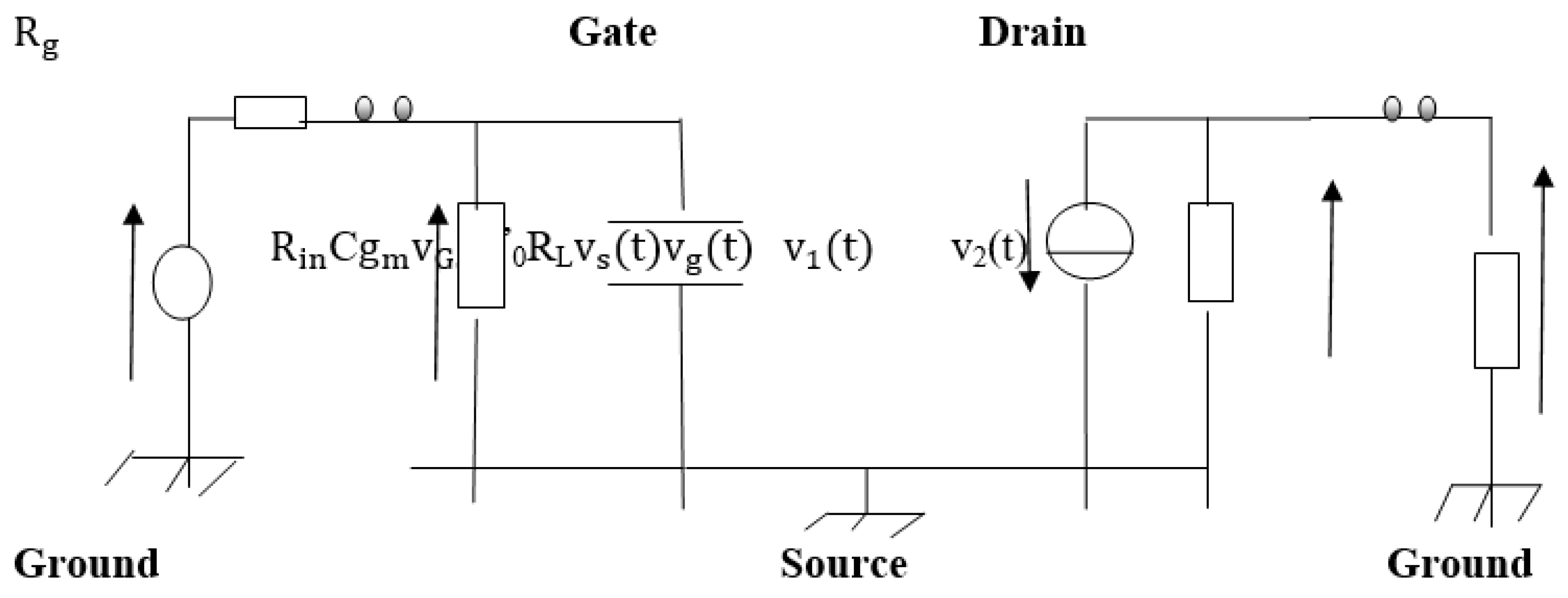
Figure 2.
Threshold voltage Vth extraction by linear extrapolation in the subthreshold region from the IDS–VGS characteristics plotted on a logarithmic scale.
Figure 2.
Threshold voltage Vth extraction by linear extrapolation in the subthreshold region from the IDS–VGS characteristics plotted on a logarithmic scale.
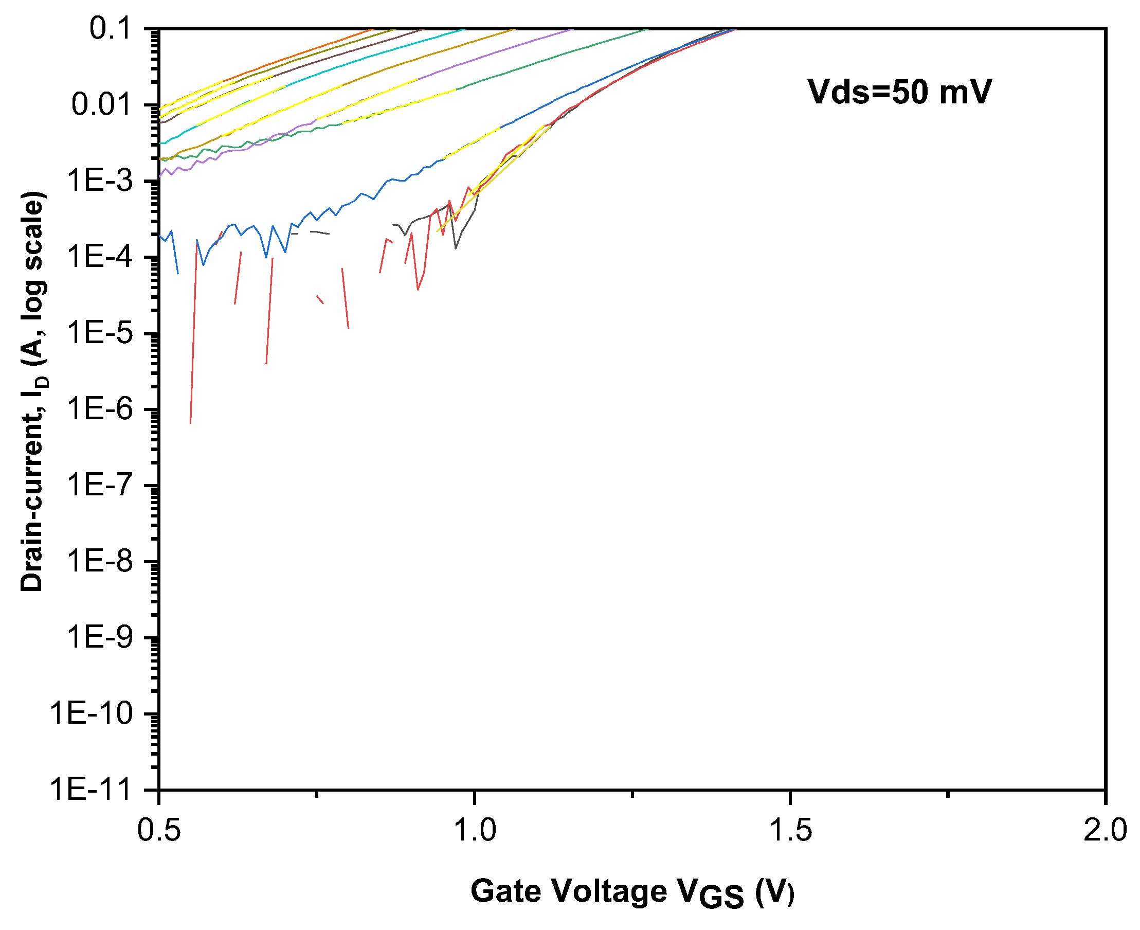
Figure 4.
Effective concentration of acceptors and interface gate-oxide density as a function of Total Ionizing Dose.
Figure 4.
Effective concentration of acceptors and interface gate-oxide density as a function of Total Ionizing Dose.
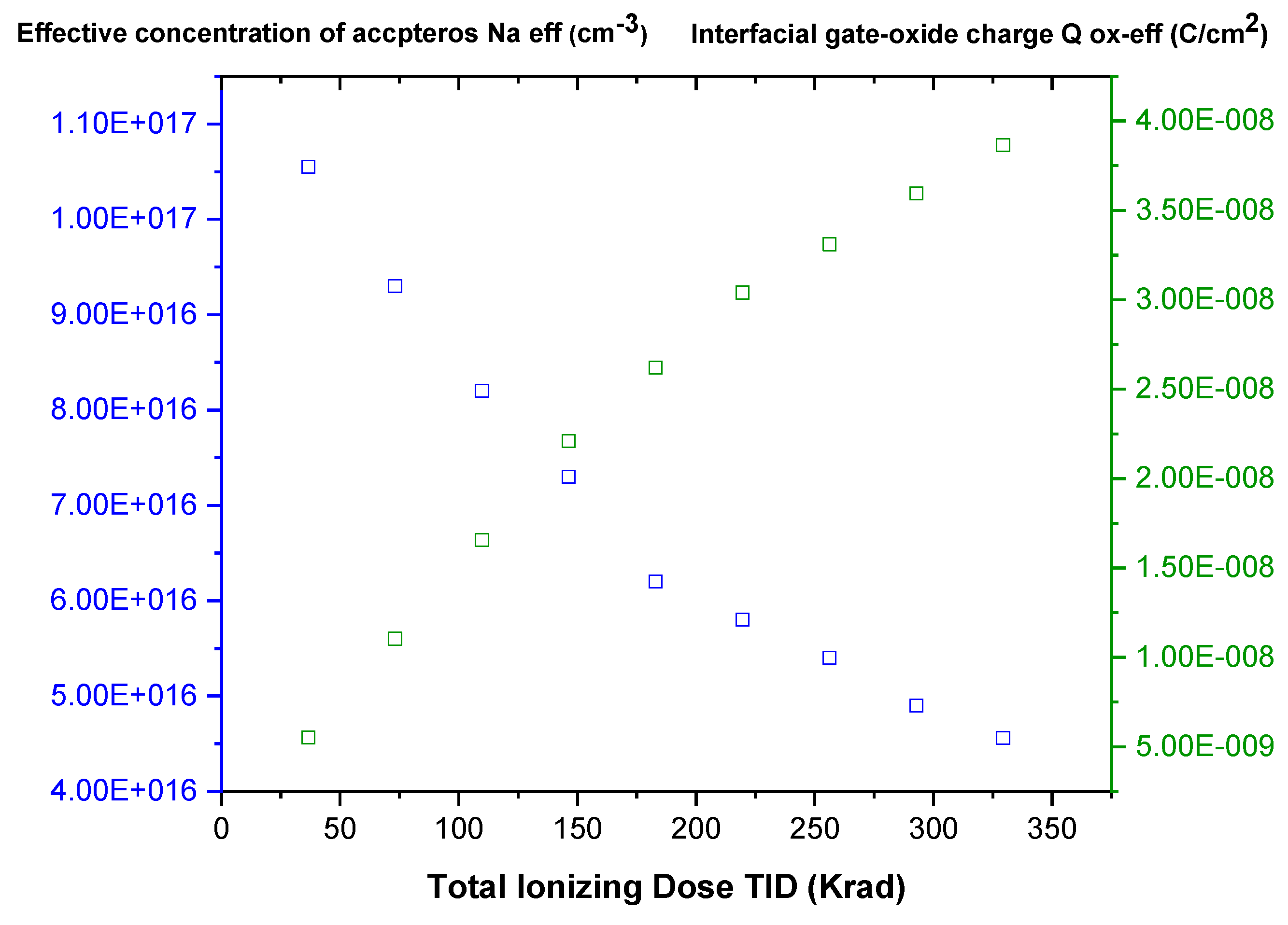
Figure 5.
The transconductance as measured versus Total Ionizing Dose in the linear regime.
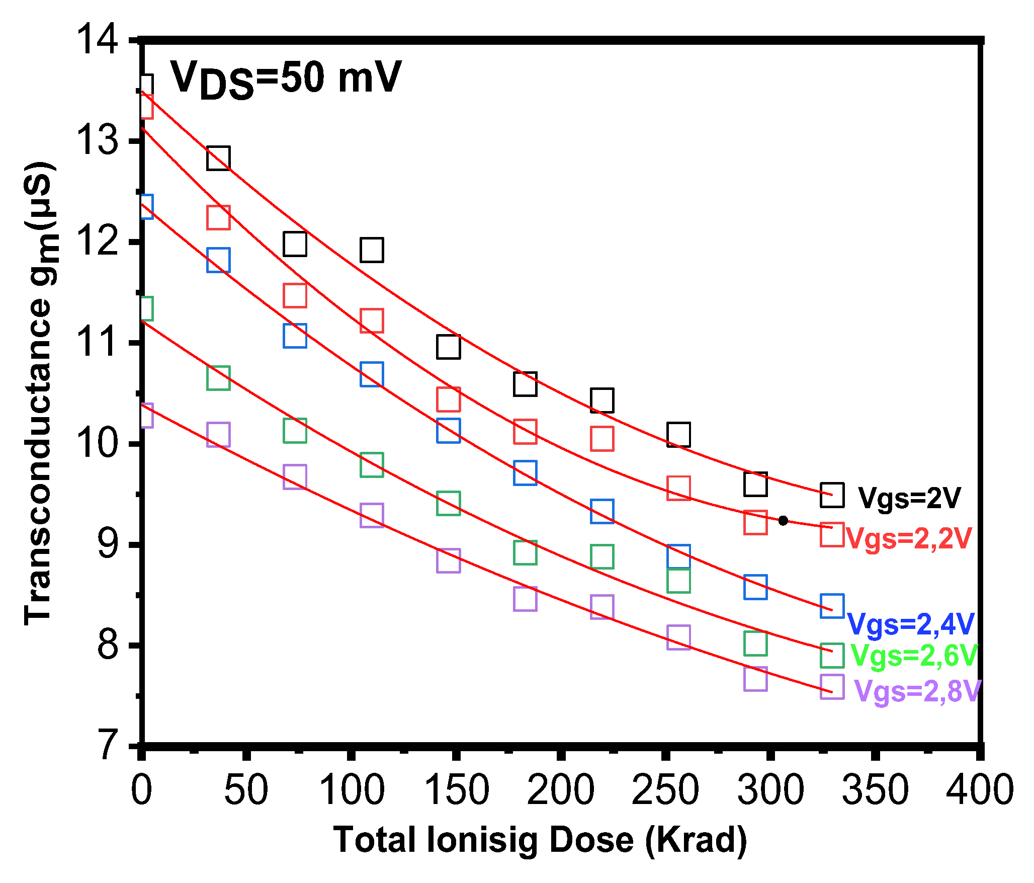
Figure 6.
The drain-current versus Total ionizing Dose in the saturation regime.
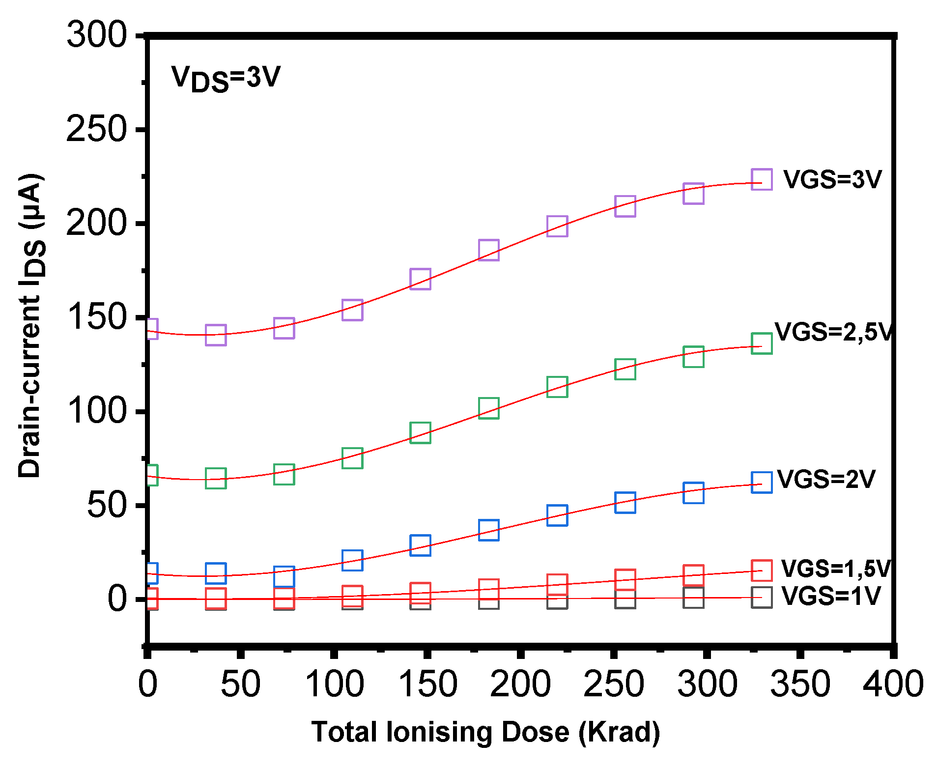
Figure 7.
The transconductance as measured versus TID in the saturation regime.
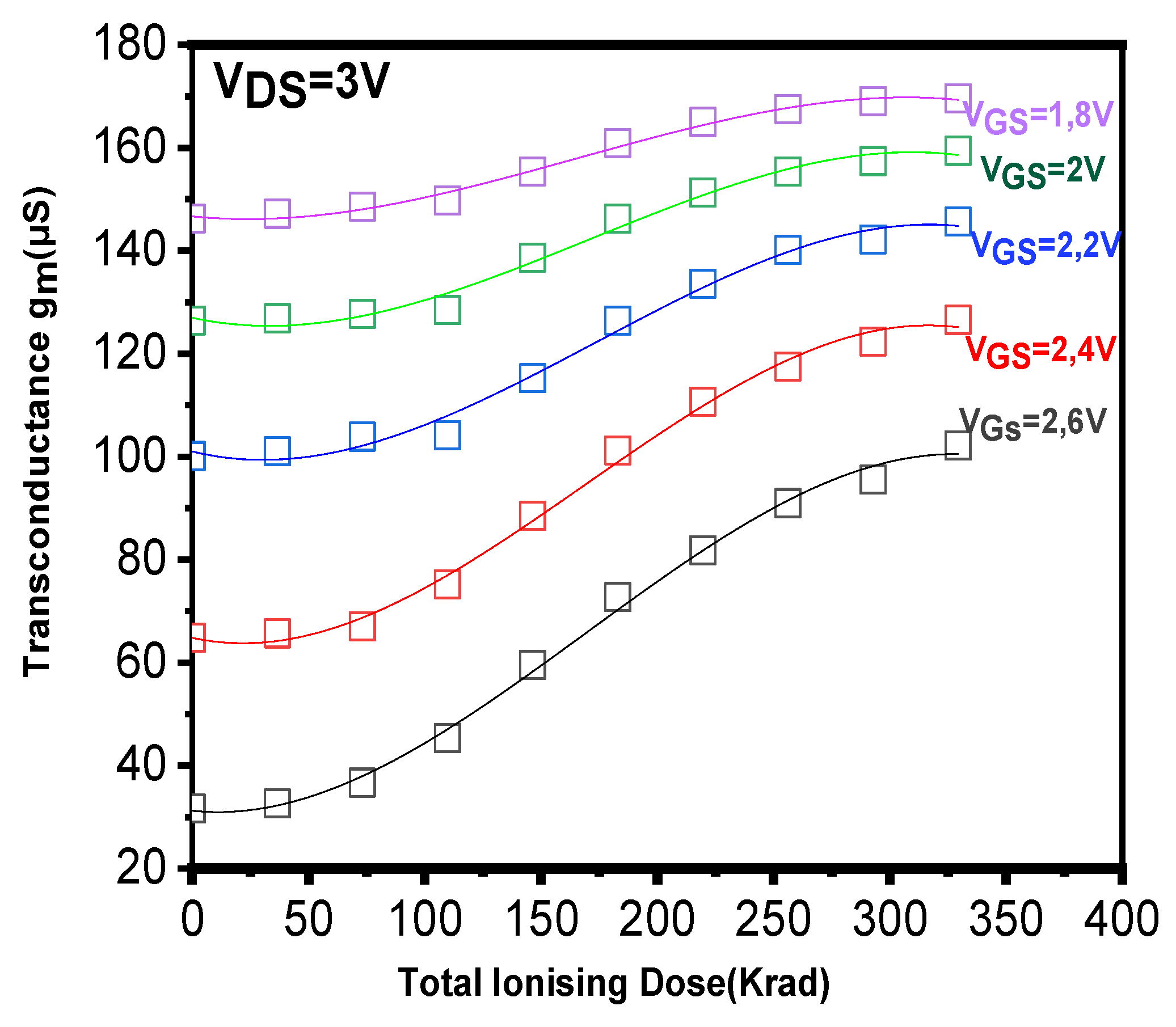
Figure 8.
The VDS-dependent conductance as obtained for TID=0 Krad and TID=348 Krad.
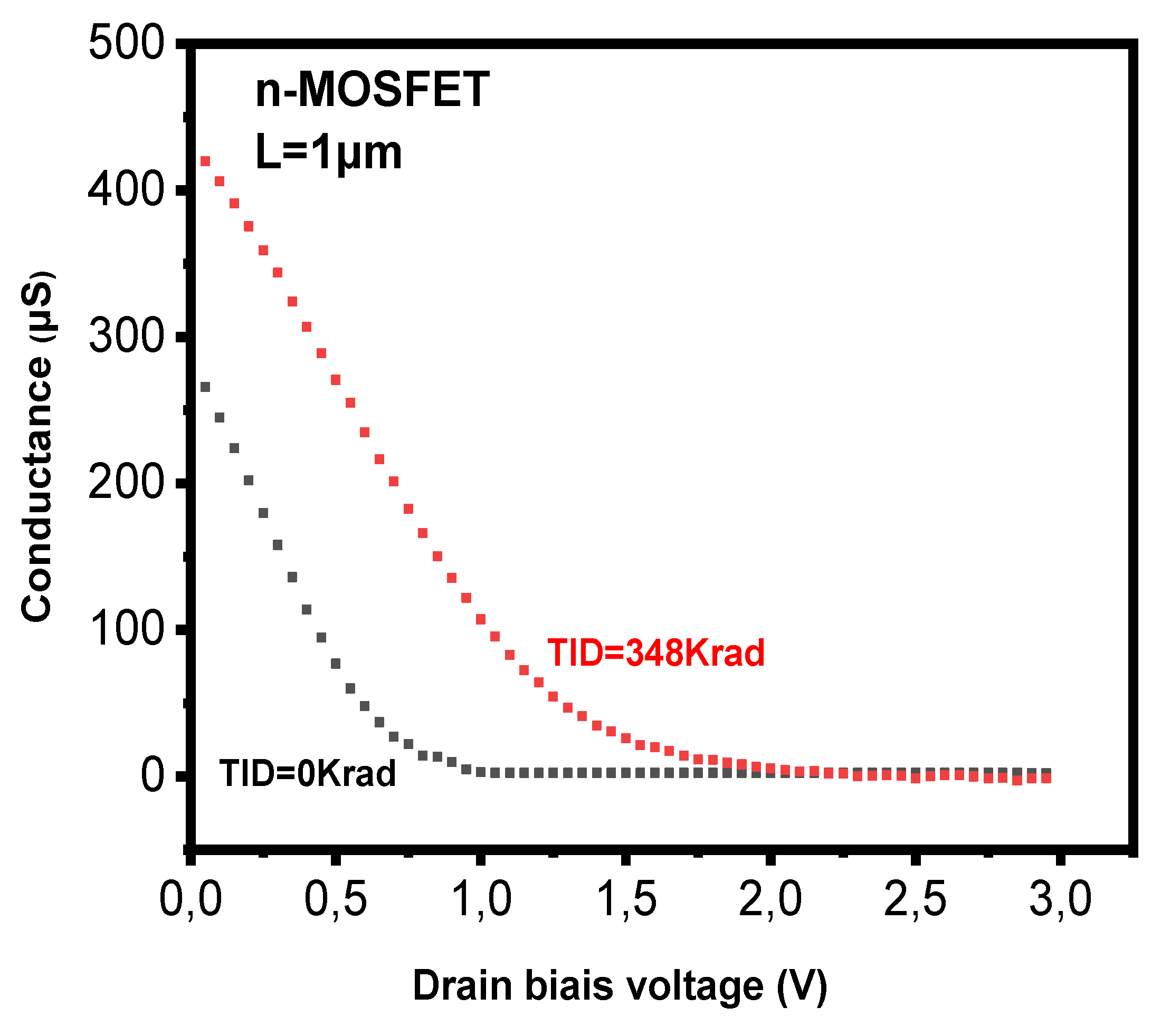
Figure 9.
input/output Impedances (a); Current/Voltage Gains (b-c) and Cutoff Frequency (d) versus TID for VGS=2V and 3V respectively.
Figure 9.
input/output Impedances (a); Current/Voltage Gains (b-c) and Cutoff Frequency (d) versus TID for VGS=2V and 3V respectively.
Disclaimer/Publisher’s Note: The statements, opinions and data contained in all publications are solely those of the individual author(s) and contributor(s) and not of MDPI and/or the editor(s). MDPI and/or the editor(s) disclaim responsibility for any injury to people or property resulting from any ideas, methods, instructions or products referred to in the content. |
© 2026 by the authors. Licensee MDPI, Basel, Switzerland. This article is an open access article distributed under the terms and conditions of the Creative Commons Attribution (CC BY) license (http://creativecommons.org/licenses/by/4.0/).
Copyright: This open access article is published under a Creative Commons CC BY 4.0 license, which permit the free download, distribution, and reuse, provided that the author and preprint are cited in any reuse.


