Submitted:
12 May 2025
Posted:
13 May 2025
You are already at the latest version
Abstract
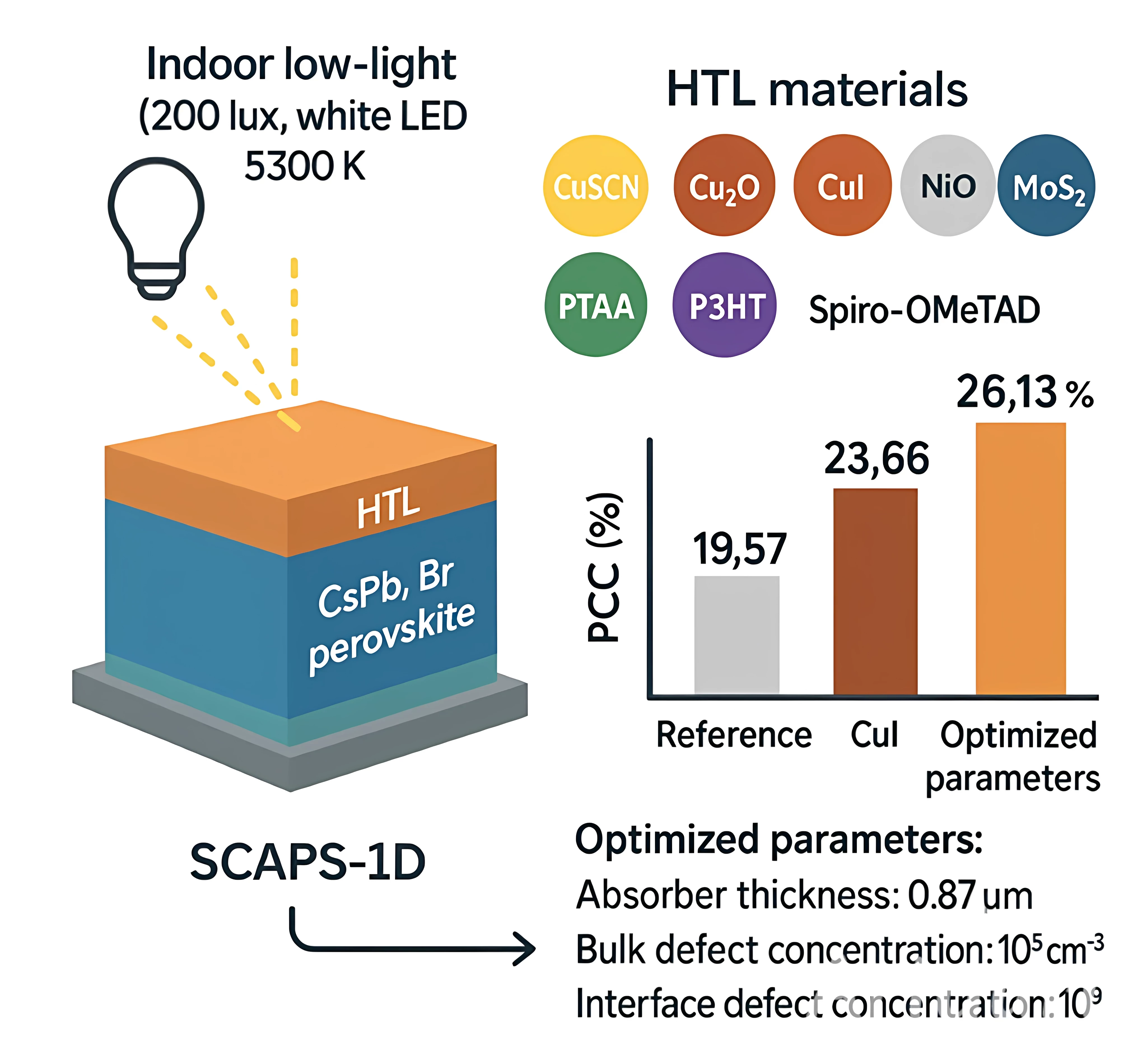
This study utilized SCAPS-1D solar simulation software to model how different hole transport layers (HTLs) affect the photoelectric conversion efficiency (PCE) of CsPbI₂Br perovskite solar cells under indoor low-light conditions. Simulation parameters include 300 K working temperature, white LED light source with 560 lux illuminance, 5700 K color temperature, equivalent to 0.661 mW/cm² power density. The investigation explores the influence of layer thickness and defect concentration on performance to identify optimal parameters. Simulation results revealed that among eight hole transport materials (CuSCN, Cu₂O, CuI, NiO, MoS₂, PTAA, P3HT, Spiro-OMeTAD), CuI achieved the best performance with open-circuit voltage (Voc) of 1.22 V, short-circuit current density (Jsc) of 0.153 mA/cm², fill factor (FF) of 83.84%, and PCE of 23.66%. Analysis of HTL and absorption layer thickness, bulk defect concentration, interface defect density, and HTL-free scenario showed that interface defect concentration and absorption layer parameters have greater influence than HTL thickness. Under optimized conditions of 0.87 μm absorption layer thickness, defect concentration of 10¹⁵ cm⁻³, and interface defect concentration of 10⁹ cm⁻³, PCE reached 26.13%, while the HTL-free structure achieved 19.57%. This study demonstrates that CuI as HTL provides excellent efficiency for CsPbI₂Br perovskite solar cells and highlights their potential in indoor low-light power generation applications.
Keywords:
CsPbI₂Br perovskite solar cells
; photoelectric conversion efficiency
; hole transport layer
; indoor low-light conditions
; defect concentration
1. Introduction
The increasing environmental awareness has elevated the importance of solar energy harvesting technologies. Among various solar cell technologies, perovskite solar cells (PSCs) have garnered significant attention due to their outstanding photoelectric conversion efficiency, low manufacturing cost, and excellent photoelectric properties [1,2]. However, conventional solar energy generation faces limitations, including inability to generate power after sunset and susceptibility to weather conditions. Indoor low-light energy harvesting presents a promising solution to overcome these limitations. Recent studies have shown that perovskite solar cells can achieve high power conversion efficiencies under indoor lighting conditions, making them promising candidates for powering Internet of Things (IoT) devices [3]. Yang et al. demonstrated that optimized perovskite compositions can maintain stable performance under various indoor lighting spectra including LED, fluorescent, and halogen sources [4]. For effective indoor light harvesting under common sources such as LEDs, solar cells require bandgaps of approximately 1.9 eV [2]. CsPbI₂Br, with a bandgap of 1.88 eV [5], emerges as an ideal absorption layer material for indoor low-light photovoltaic applications. The thermal and phase stability of CsPbI₂Br has been significantly improved through various strategies including compositional engineering and interface modification [6]. Comparative studies have shown that CsPbI₂Br maintains its black phase at room temperature longer than CsPbI₃, while still offering a suitable bandgap for both outdoor and indoor applications [7]. Recent experimental studies by Bahadur et al. [8] demonstrated that CsPbI₂Br-based devices achieved power conversion efficiencies exceeding 20% under 1000 lux fluorescent lighting, highlighting their practical potential for indoor applications. Liu et al. [9] further improved device stability through compositional engineering, addressing a critical challenge in perovskite technology.
Unlike its performance under standard AM 1.5G illumination where conversion efficiency typically ranges between 17-19%, CsPbI₂Br-based solar cells demonstrate superior performance under indoor lighting conditions, with potential photoelectric conversion efficiencies reaching up to 34.2% when paired with appropriate HTLs [10]. Experimental work by Wang et al. [11] confirmed this trend, showing that optimized CsPbI₂Br devices maintained over 90% of their initial efficiency after 1000 hours under continuous indoor illumination, outperforming their outdoor stability metrics. While the absorption layer plays a crucial role in determining efficiency, the electron transport layer (ETL) and HTL significantly impact overall device performance. Traditionally, TiO₂ has been widely employed as an ETL, but its instability and high-temperature processing requirements have led to the consideration of SnO₂ as a superior alternative due to its enhanced photoelectric stability and low-temperature processing compatibility. Zhang et al. [12] experimentally validated this transition, demonstrating that SnO₂-based devices exhibited 15% higher stability under operational conditions compared to TiO₂ counterparts. The fundamental functions of HTLs include hole extraction and transport, prevention of electron flow toward the anode, and protection of the perovskite layer from moisture and oxygen [13]. Recent research has focused on developing low-cost, dopant-free hole transport materials that can enhance both efficiency and stability of perovskite solar cells [14]. Additionally, inorganic hole transport layers have gained attention for their superior environmental stability compared to organic counterparts, potentially enabling longer device lifetimes under various operating conditions [15].
Device simulation software like SCAPS-1D (Solar Cell Capacitance Simulator) provides a cost-effective approach to optimize solar cell structures and identify promising material combinations before experimental validation. Beyond SCAPS-1D, researchers have employed various simulation tools to model perovskite solar cell performance, including finite element analysis and drift-diffusion modeling [16]. These complementary approaches have enabled comprehensive understanding of carrier dynamics and recombination mechanisms in perovskite devices [17]. Previous studies have demonstrated the efficacy of SCAPS-1D in modeling CsPbI₂Br-based solar cells with various ETL and HTL configurations. Pinzón et al. [5] optimized all-inorganic inverted CsPbI₂Br and CsPbI₃ perovskite solar cells, identifying optimal material thicknesses and defect densities that significantly enhanced conversion efficiencies. Similarly, Khatoon et al. [18] modeled single, dual, and triple-layer absorption structures incorporating CsPbI₂Br and achieved substantial efficiency improvements through parameter optimization. This study employs SCAPS-1D simulation to investigate the impact of various hole transport layers on CsPbI₂Br perovskite solar cell performance under indoor low-light conditions (white LED, 560 lux, 5700K color temperature, 0.661 mW/cm²). By examining both organic and inorganic HTL materials and optimizing critical parameters such as layer thickness and defect concentrations, this research aims to identify the most efficient device structure for indoor photovoltaic applications.
2. Device Structure and Simulation Parameters
2.1. Device Structure
The solar cell device architecture investigated in this study followed a standard n-i-p configuration consisting of FTO/SnO₂/CsPbI₂Br/Au (Figure 1a) and add HTL layer FTO/SnO₂/CsPbI₂Br/HTL/Au with HTL incorporation (Figure 1b). Fluorine-doped tin oxide (FTO) served as the transparent conductive substrate with a thickness of 0.2 μm. Tin oxide (SnO₂) was employed as the ETL with a thickness of 0.2 μm, selected for its favorable band alignment, superior stability, and compatibility with low-temperature processing compared to traditional TiO₂-based ETLs. The photoactive layer consisted of CsPbI₂Br perovskite with an initial thickness of 0.5 μm, chosen for its optimal bandgap of 1.88 eV which is particularly well-suited for indoor light harvesting. Eight different materials were systematically investigated as HTLs, including five inorganic candidates (CuSCN, Cu₂O, CuI, NiO, and MoS₂) and three organic alternatives (PTAA, P3HT, and Spiro-OMeTAD), each with a standardized thickness of 0.2 μm for initial comparative analysis. The inorganic HTLs were selected for their promising stability characteristics, while the organic HTLs were chosen based on their established performance in perovskite solar cells. Gold (Au) with a work function of 5.1 eV was used as the counter electrode to complete the device structure. For comprehensive analysis, a reference structure without any HTL (FTO/SnO₂/CsPbI₂Br/Au) was also simulated to evaluate the fundamental necessity and contribution of the hole transport layer to overall device performance under indoor low-light conditions.
2.2. Numerical Method
The SCAPS-1D simulation is based on solving three fundamental semiconductor equations: Poisson's equation, and continuity equations for both holes and electrons, as shown below [19]:
Where, ε is the dielectric constant, q is the electron charge, NA and ND are acceptor and donor type density respectively, φ is the electrostatic potential, p, n, ρp, ρn, Jp, Jn are hole concentration, electron concentration, hole distribution, electron distribution, current densities of hole and current densities of electron respectively. Gop is the optical generation rate, R is the net recombination rate from both direct and indirect recombination processes. All of these parameters are the function of the position coordinate x.
This study employed SCAPS-1D (version 3.3.11) to simulate CsPbI₂Br perovskite solar cells under indoor low-light conditions (300 K, white LED, 560 lux, 5700 K color temperature, 0.661 mW/cm²). The key material parameters for the primary structural layers are summarized in Table 1. The physical parameters for the investigated HTL materials are presented in Table 2, including both inorganic (CuSCN, Cu₂O, CuI, NiO, MoS₂) and organic (PTAA, P3HT, Spiro-OMeTAD) materials, each with a thickness of 0.2 μm. Interface properties between the absorber and adjacent transport layers were configured as shown in Table 3, with neutral defect types assigned and a total defect density of 1.0×10⁹ cm⁻³ at these critical interfaces.
3. Results and Discussion
3.1. CsPbI₂Br Perovskite Solar Cells Energy Band Diagram and Performance Comparison of Different HTLs
Figure 2 illustrates the energy band diagram of CsPbI₂Br perovskite solar cells, revealing the mechanism governing electron-hole transport. Efficient separation and transport of carriers are critical for enhancing photoelectric conversion efficiency [1,2]. Electrons migrate from the absorption layer (CsPbI₂Br) toward the electron transport layer (SnO₂), while holes move toward the HTL. For optimal carrier transport, the conduction band minimum (CBM) of the absorption layer must exceed that of the electron transport layer, and the valence band maximum (VBM) of the absorption layer must exceed that of the hole transport layer. This energy band alignment promotes effective carrier separation while reducing recombination losses, thereby enhancing overall solar cell performance.
The performance of eight different HTL materials in the FTO/SnO₂/CsPbI₂Br/HTL/Au structure under indoor low-light conditions (0.661 mW/cm²) is summarized in Table 4. CuI demonstrated superior performance, achieving an Voc of 1.22 V, FF of 83.84%, Jsc of 0.153 mA/cm², and PCE of 23.66%. Other materials exhibited PCE values between 21.34% and 22.21%. CuI's exceptional performance can be attributed to several factors: (1) its moderate bandgap (3.1 eV) and optimal energy band positions create favorable alignment with the absorption layer, facilitating efficient hole transport; (2) its high hole mobility (43.9 cm²/V·s) enables rapid carrier extraction. Although MoS₂ features higher hole mobility (150 cm²/V·s), its suboptimal band alignment with CsPbI₂Br results in lower PCE. Among organic materials, PTAA achieved the highest efficiency (22.05%) with comparable hole mobility (40 cm²/V·s) to CuI, but its energy band alignment and lower fill factor limited overall performance.
To investigate performance under varying illumination intensities, simulations were conducted at two additional white LED light sources: 200 lux (0.0661 mW/cm²) and 1000 lux (0.384 mW/cm²). Results are presented in Table 4 and Table 5. With decreasing light intensity, all efficiency parameters declined correspondingly, with Jsc showing the most significant reduction [3,4]. At 0.384 mW/cm², PCE values ranged between 21.14% and 22.57%, with CuI maintaining superior performance. At 0.0661 mW/cm², PCE decreased to 19.51%-20.33%, with P3HT performing marginally better than other materials. To determine the threshold light intensity affecting PCE, simulations were conducted across power densities from 0 to 1 mW/cm² (Figure 3). Even at extremely low intensities, PCE remained above 19%, with CuI consistently exhibiting optimal performance at medium to high power densities. Based on these findings, CuI was selected for further parameter optimization.
Figure 4 displays the external quantum efficiency (EQE) curve of CsPbI₂Br perovskite solar cells, revealing optimal photoelectric conversion in the 350-650 nm wavelength range. This spectral response aligns precisely with the primary emission spectrum of indoor LED light sources, explaining why CsPbI₂Br solar cells perform better under indoor illumination than standard AM 1.5G solar spectrum. Simulation using AM 1.5G spectrum showed a significant PCE decrease from 23.66% to 17.47%. These findings align with recent literature—Pinzón et al. [5] demonstrated that CuI forms optimal band alignment with CsPbI₂Br, while Guo et al. [10] confirmed that CsPbI₂Br solar cells achieve substantially higher efficiencies under indoor lighting (up to 34.2%) compared to standard sunlight conditions (17-19%).
3.2. Performance Parameter Optimization and Structure Analysis of CsPbI₂Br Solar Cells
After identifying CuI as the optimal HTL material, we systematically investigated key parameters affecting device performance. Figure 5 demonstrates the effect of HTL thickness on solar cell performance. Once the thickness exceeds 0.04 μm, PCE changes become minimal. This suggests that HTL thickness can be reduced to 0.04 μm without compromising performance, reducing material costs and simplifying fabrication. Figure 6 shows that as absorption layer thickness increases from 0.2 μm to approximately 1 μm, PCE gradually improves and stabilizes. Beyond 1.2 μm, PCE decreases due to increased carrier recombination and series resistance. Additionally, thicker absorption layers typically exhibit higher defect densities. Based on these findings, the optimal configuration includes HTL thickness of 0.04 μm and absorption layer thickness of 1 μm, enhancing PCE to 26.3%.
Figure 7 analyzes the influence of CuI's shallow acceptor density on device performance. When the concentration exceeds 10¹⁷ cm⁻³, PCE begins to decline, decreasing by approximately 3% at 10¹⁹ cm⁻³. Excessive doping can disrupt energy band alignment, increase recombination rates, or create rough interfaces that increase leakage current [13,14]. Therefore, the optimal doping concentration ranges between 10¹⁵ and 10¹⁷ cm⁻³. As shown in Figure 8, the absorption layer's defect concentration has a more pronounced effect on PCE. When defect concentration exceeds 10¹⁵ cm⁻³, PCE drops dramatically, with potential decreases of up to 8%. Additionally, the interface defect concentration between the absorption layer and HTL significantly impacts performance. Figure 9 demonstrates that once the interface defect concentration exceeds 10¹² cm⁻³, PCE noticeably decreases by up to 4%, highlighting the importance of interface engineering for high-efficiency devices [15].
Under optimized conditions -HTL thickness of 0.04 μm, absorption layer thickness of 0.87 μm, HTL doping concentration of 10¹⁷ cm⁻³, absorption layer defect concentration of 10¹⁵ cm⁻³, and interface defect concentration of 10⁹ cm⁻³—CsPbI₂Br solar cells under indoor low-light conditions achieved a PCE of 28.57%, with Voc of 1.2468 V, Jsc of 0.17043 mA/cm², and FF of 88.90%. To evaluate the necessity of HTL, we simulated an HTL-free structure (FTO/SnO₂/CsPbI₂Br/Au), which yielded a PCE of 17.6%, Voc of 0.8759 V, Jsc of 0.15306 mA/cm², and FF of 86.81%—6% less efficient than the CuI-HTL structure. Figure 10 compares the J-V curves of both structures, revealing that the open-circuit voltage of the HTL-free structure is approximately 28% lower than the CuI-HTL structure (0.8759 V vs. 1.22 V). This indicates that while certain HTL parameters have minimal impact on PCE, the HTL layer itself significantly contributes to overall device performance.
3.3. Literature Comparison
To verify the reliability of our simulation results, we compared our optimized CsPbI₂Br perovskite solar cell structure with recent experimental findings (Table 6 and Table 7). Under standard AM 1.5G solar spectrum, our optimized FTO/SnO₂/CsPbI₂Br/CuI/Au structure achieved a simulated PCE of 19.48%, Voc of 1.376 V, Jsc of 16.35 mA/cm², and FF of 86.57% -all exceeding parameters reported in literature for similar structures. Compared to the FTO/TiO₂/CsPbI₂Br/MoO₂-PTAA/Carbon structure reported by Lee et al. [24] (PCE of 14.67%), our simulated structure shows approximately 33% higher efficiency. Similarly, compared to the structure using Spiro-OMeTAD as HTL reported by Chen et al. [26] (PCE of 15.03%), our structure demonstrates approximately 30% higher efficiency. This performance difference can be attributed to several factors: (1) CuI forms more ideal energy band alignment with CsPbI₂Br, facilitating efficient charge separation; (2) our systematic optimization of interface defect concentration reduced recombination losses; and (3) optimized layer thickness configuration balances light absorption and charge transport requirements. The disparity between simulation and experimental results can be partially attributed to practical fabrication challenges such as film uniformity, interface roughness, and environmental factors that are not accounted for in simulations.
Notably, our optimized solar cells exhibit significantly higher PCE (28.57%) under indoor low-light conditions (0.661 mW/cm²) than under standard AM 1.5G solar spectrum (19.48%). While the short-circuit current density under indoor conditions (0.17043 mA/cm²) is far lower than under standard illumination (16.35 mA/cm²), this is explained by the PCE calculation formula:
PCE = (Voc × Jsc × FF)/Pin
Given that the indoor power density (0.661 mW/cm²) is only about 0.661% of standard AM 1.5G (100 mW/cm²), the ratio of short-circuit current densities (approximately 1:96) is consistent with the ratio of light source power densities (approximately 1:151). Under low-light conditions, despite significantly lower short-circuit current density, the relatively high open-circuit voltage and fill factor, combined with the substantially lower denominator in Equation 4, result in higher calculated PCE.
More significantly, the bandgap of CsPbI₂Br (1.88 eV) is particularly well-suited for indoor low-light spectral distribution [2,5]. As shown in Figure 4, this material exhibits optimal photoelectric conversion in the 350-650 nm range, corresponding closely to the emission spectrum of indoor LED light sources. In contrast, the standard AM 1.5G solar spectrum contains significant long-wavelength components that CsPbI₂Br cannot effectively absorb. Compared to literature reports, the indoor low-light PCE of our optimized structure (28.57%) exceeds the 23.51% reported by Kim et al. [28] and the 23.24% reported by Bahadur et al. [27], further confirming the theoretical advantages of CuI as an HTL material in CsPbI₂Br perovskite solar cells for indoor applications.
4. Conclusion
This research utilized SCAPS-1D simulation software to investigate the impact of various HTLs on the PCE of CsPbI₂Br perovskite solar cells under indoor low-light conditions (white LED, 560 lux, 0.661 mW/cm²). The study compared eight HTL materials (CuSCN, Cu₂O, CuI, NiO, MoS₂, PTAA, P3HT, and Spiro-OMeTAD) across varying light intensities (0-1 mW/cm²). Results demonstrated that CuI exhibited superior energy level compatibility with the absorption layer and the highest PCE of 23.66%, attributed to its optimal band alignment and high hole mobility. CuI also demonstrated better stability and higher PCE compared to other materials across most low-light intensity ranges. Parameter optimization revealed that HTL thickness has minimal impact on efficiency and can be reduced to 0.04 μm, while absorption layer thickness, defect concentration, and interface defect density significantly influenced performance. Under optimized conditions (absorption layer: 0.87 μm, defect concentration: 10¹⁵ cm⁻³, interface defect concentration: 10⁹ cm⁻³), the PCE increased to 28.57% with Voc of 1.2468 V, Jsc of 0.17043 mA/cm², and FF of 88.90%. The HTL-free structure showed reduced efficiency (19.57%) and open-circuit voltage (0.8759 V), confirming HTL's crucial role in device performance. This study confirms CuI as the optimal HTL for CsPbI₂Br perovskite solar cells in indoor applications and demonstrates that optimization of material quality and device structure can substantially improve conversion efficiency. The findings highlight CsPbI₂Br perovskite solar cells' potential for powering low-power electronics in indoor environments where conventional solar cells perform poorly. Future research should focus on experimental validation and development of scalable fabrication techniques.
Author Contributions
[Chih-Hsi Peng]: Methodology, Formal analysis, Writing - original draft; [Yi-Cheng Lin]: Conceptualization, Resources, Writing - review & editing.
Research Data Policy and Data Availability Statements
The computational data and simulation parameters used in this study are available from the corresponding author upon reasonable request. The SCAPS-1D software used for the simulations is freely available from the University of Gent. All other data generated or analyzed during this study are included in this published article.
Acknowledgments
The authors wish to thank the developers of SCAPS at the University of Gent for making their software package publicly available free of charge. The authors also like to acknowledge the financial support from National Science and Technology Council under grant number 113-2221-E-018 -001.
Compliance with Ethical Standards
The authors declare that this research was conducted in accordance with ethical standards. No human or animal subjects were involved in this study. All computational methods and data analysis procedures followed established scientific practices.
Competing Interests
The authors declare that they have no known competing financial interests or personal relationships that could have appeared to influence the work reported in this paper.
References
- Alanazi, T.i.; Shaker, A.; Zein, W. Design and Simulation of 2D Ruddlesden-Popper Perovskite Solar Cells under LED Illumination: Role of ETL and Front Contact Band Alignment, Sol. Energy Mater. Sol. Cells 2024, 274, 112992. [Google Scholar] [CrossRef]
- Wu, M.J.; Kuo, C.C.; Jhuang, L.S.; Chen, P.H.; Lai, Y.F.; Chen, F.C. Bandgap engineering enhances the performance of mixed-cation perovskite materials for indoor photovoltaic applications. Adv. Energy Mater. 2019, 9, 1901863. [Google Scholar] [CrossRef]
- Yang, M.; Kim, D.; Park, Y. High-efficiency perovskite solar cells for indoor photovoltaic applications: Recent progress and challenges. Energy Environ. Sci. 2021, 14, 643–654. [Google Scholar] [CrossRef]
- Zhang, L.; Wang, J.; Liu, T. Spectral response optimization of perovskite photovoltaics for indoor light harvesting. Adv. Energy Mater. 2021, 11, 2100332. [Google Scholar]
- Pinzón, C.; Martínez, N.; Casas, G.; Alvira, F.C.; Denon, N.; Brusasco, G.; Cappelletti, M.A. Optimization of inverted all-inorganic CsPbI3 and CsPbI2Br perovskite solar cells by SCAPS-1D simulation. Solar 2022, 2, 559–571. [Google Scholar] [CrossRef]
- Wang, R.; Xue, J.; Wang, K.L. Phase stability engineering of CsPbI₂Br perovskites for photovoltaic applications. J. Phys. Chem. Lett. 2021, 12, 1465–1472. [Google Scholar]
- Huang, S.; Zhang, B.; Wu, Y. Comparative study of all-inorganic cesium lead halide perovskites for indoor photovoltaic applications. ACS Appl. Mater. Interfaces 2021, 13, 43833–43841. [Google Scholar]
- Bahadur, J.; Cho, S.; Pandey, P.; Yoon, S.; Lee, D.G.; Ryu, J.; Kang, D.W. Fully hot Air-Processed All-Inorganic CsPbI2Br perovskite solar cells for outdoor and indoor applications. Appl. Surf. Sci. 2025, 684, 161909. [Google Scholar] [CrossRef]
- Liu, Y.; Lang, K.; Han, H.; Liu, H.; Fu, Y.; Zou, P.; Yao, J. Crystallization management of CsPbI2Br perovskites by PbAc2-incorporated twice spin-coating process for efficient and stable CsPbI2Br perovskite solar cells. J. Energy Chem. 2024, 97, 419–428. [Google Scholar] [CrossRef]
- Guo, Z.; Jena, A.K.; Takei, I.; Ikegami, M.; Ishii, A.; Numata, Y.; Miyasaka, T. Dopant-free polymer HTM-based CsPbI2Br solar cells with efficiency over 17% in sunlight and 34% in indoor light. Adv. Funct. Mater. 2021, 31, 2103614. [Google Scholar] [CrossRef]
- Wang, K.L.; Zhou, Y.H.; Lou, Y.H.; Wang, Z.K. Perovskite indoor photovoltaics: opportunity; challenges. Sci. C. 2021, 12, 11936–11954. [Google Scholar] [CrossRef] [PubMed]
- Huy, V.P.H.; Nguyen, T.M.H.; Bark, C.W. Recent Advances of Doped SnO2 as Electron Transport Layer for High-Performance Perovskite Solar Cells. Materials 2023, 16, 6170. [Google Scholar]
- Dong, Y.; Duan, J.; Luo, D.; Liu, J.; Wang, X.; Liu, X.; Gao, Y. Interface optimization of CsPbI2Br based perovskite solar cells by device simulation. Mater. Today Commun. 2024, 39, 108695. [Google Scholar] [CrossRef]
- Li, N.; Niu, X.; Ding, L. Emerging dopant-free hole transport materials for perovskite solar cells. Energy Environ. Sci. 2020, 13, 3608–3620. [Google Scholar]
- Kim, H.; Zhao, J.; Du, M. Long-term stable inorganic hole transport layers for efficient perovskite solar cells. Adv. Funct. Mater. 2020, 30, 2002674. [Google Scholar]
- Lopez-Varo, P.; Jiménez-Tejada, J.A.; García-Rosell, M. Device physics of perovskite solar cells: Theory and experiment. Adv. Energy Mater. 2020, 10, 1903555. [Google Scholar] [CrossRef]
- Xing, G.; Wu, Y.; Li, X. Multi-scale simulation approaches for perovskite photovoltaics: From material properties to device performance. J. Mater. Chem. A 2021, 9, 17545–17570. [Google Scholar]
- Khatoon, S.; Chakraborty, V.; Yadav, S.K.; Diwakar, S.; Singh, J.; Singh, R.B. Simulation study of CsPbIxBr1-x and MAPbI3 heterojunction solar cell using SCAPS-1D. Sol. Energy 2023, 254, 137–157. [Google Scholar]
- Basak, A.; Singh, U.P. Numerical modelling and analysis of earth abundant Sb₂S₃ and Sb₂Se₃ based solar cells using SCAPS-1D. Sol. Energy Mater. Sol. Cells 2021, 230, 111184. [Google Scholar] [CrossRef]
- Siddique, M.; Sultan, M.; Safeer, S.H. Device Optimization of CsPbI 2 Br-based Inorganic Perovskite Solar Cells using Different Hole and Electron Transport Layers via SCAPS-1D. 2024. [Google Scholar]
- Sharma, D.; Mehra, R.; Raj, B. Comparative study of hole transporting layers commonly used in high-efficiency perovskite solar cells. J. Mater. Sci. 2022, 57, 21172–21191. [Google Scholar] [CrossRef]
- Raoui, Y.; Ez-Zahraouy, H.; Ahmad, S.; Kazim, S. Unravelling the theoretical window to fabricate high performance inorganic perovskite solar cells, Sustain. Energy Fuels 2021, 5, 219–229. [Google Scholar]
- Chen, Y.; Liu, J.; Wu, Y.; Wang, Z.; Li, J.; Liu, X.; Wang, X. Performance enhancement of inverted CsPbI2Br perovskite solar cells via butylammonium cation additive modification. Mater. Lett. 2025, 379, 137643. [Google Scholar] [CrossRef]
- Lee, D.S.; Ki, M.J.; Lee, H.J.; Park, J.K.; Hong, S.Y.; Kim, B.W.; Im, S.H. Fully scalable and stable CsPbI2Br solar cells realized by an all-spray-coating process. ACS Appl. Mater. Interfaces 2022, 14, 7926–7935. [Google Scholar] [CrossRef] [PubMed]
- Dong, C.; Han, X.; Li, W.; Qiu, Q.; Wang, J. Anti-solvent assisted multi-step deposition for efficient and stable carbon-based CsPbI2Br all-inorganic perovskite solar cell. Nano Energy 2019, 59, 553–559. [Google Scholar] [CrossRef]
- Chen, H.; Ma, Y.; Wang, X.; Yao, G.; Du, Y.; Zhou, J.; Dai, S. Improving the stability and efficiency of inorganic CsPbI2Br perovskite via surface reconstruction strategy. Chem. Eng. J. 2022, 442, 136242. [Google Scholar] [CrossRef]
- Bahadur, J.; Cho, S.; Pandey, P.; Ryu, J.; Yoon, S.; Lee, D.G.; Kang, D.W. Surface defect passivation of All-Inorganic CsPbI2Br perovskites via fluorinated ionic liquid for efficient Outdoor/Indoor photovoltaics processed in ambient air. Appl. Surf. Sci. 2023, 637, 157901. [Google Scholar] [CrossRef]
- Kim, K.S.; Jin, I.S.; Park, S.H.; Lim, S.J.; Jung, J.W. Methylammonium iodide-mediated controlled crystal growth of CsPbI2Br films for efficient and stable all-inorganic perovskite solar cells. ACS Appl. Mater. Interfaces 2020, 12, 36228–36236. [Google Scholar] [CrossRef]
Figure 1.
Schematic diagram of the proposed perovskite solar cell structures: (a) without HTL configuration, (b) with HTL configuration.
Figure 1.
Schematic diagram of the proposed perovskite solar cell structures: (a) without HTL configuration, (b) with HTL configuration.
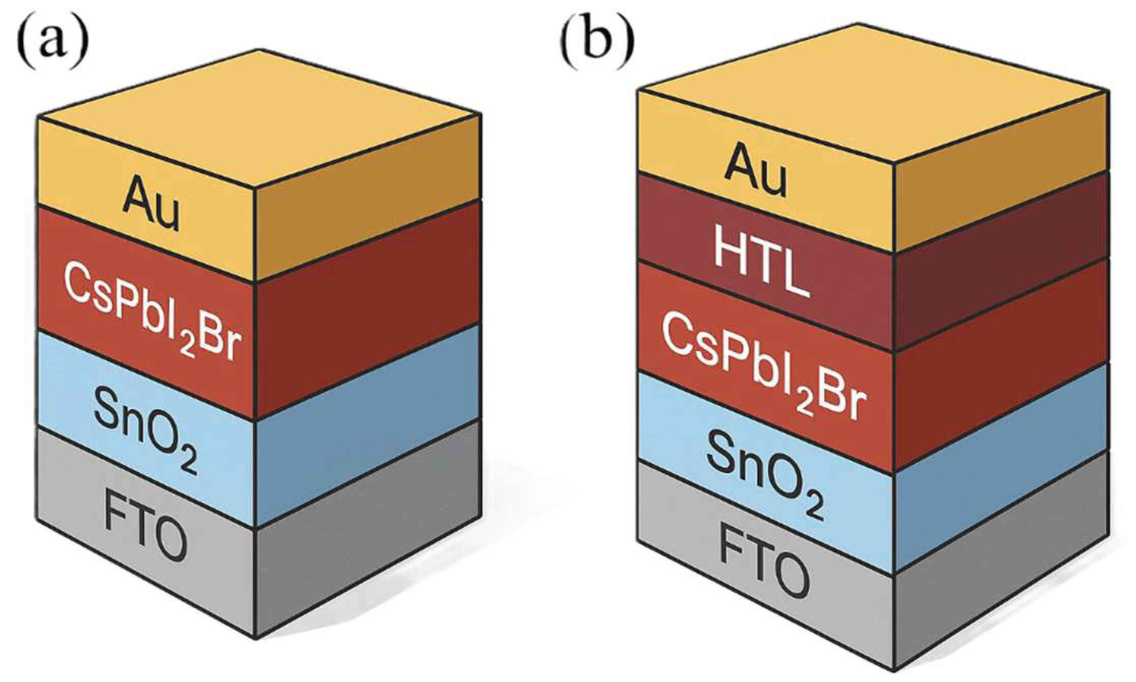
Figure 2.
Energy band diagram of CsPbI₂Br perovskite solar cells showing electron and hole transport mechanisms.
Figure 2.
Energy band diagram of CsPbI₂Br perovskite solar cells showing electron and hole transport mechanisms.
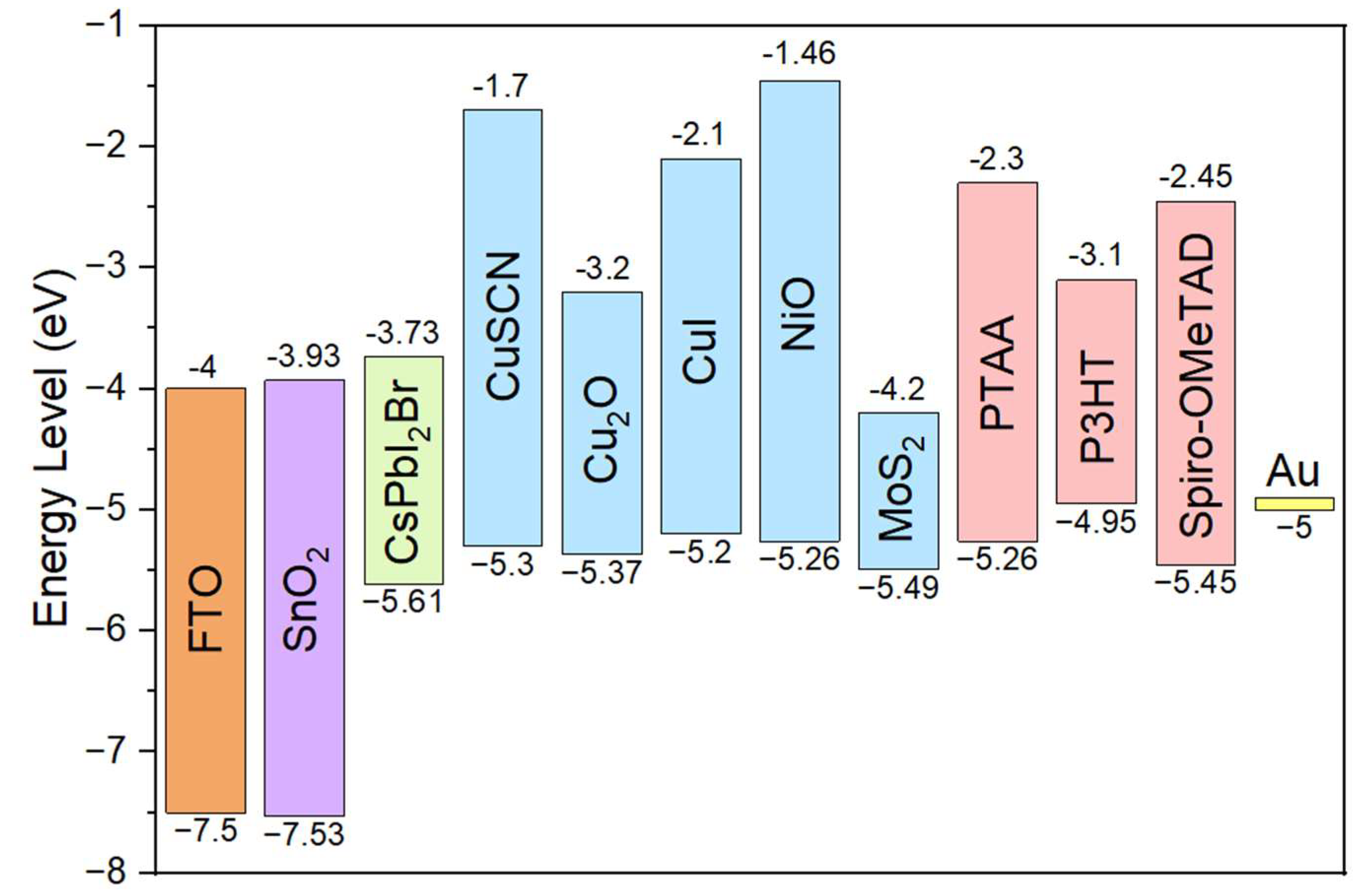
Figure 3.
Performance parameters of CsPbI₂Br perovskite solar cells with different HTLs as a function of light intensity: (a) PCE, (b) Voc, (c) Jsc, and (d) FF.
Figure 3.
Performance parameters of CsPbI₂Br perovskite solar cells with different HTLs as a function of light intensity: (a) PCE, (b) Voc, (c) Jsc, and (d) FF.
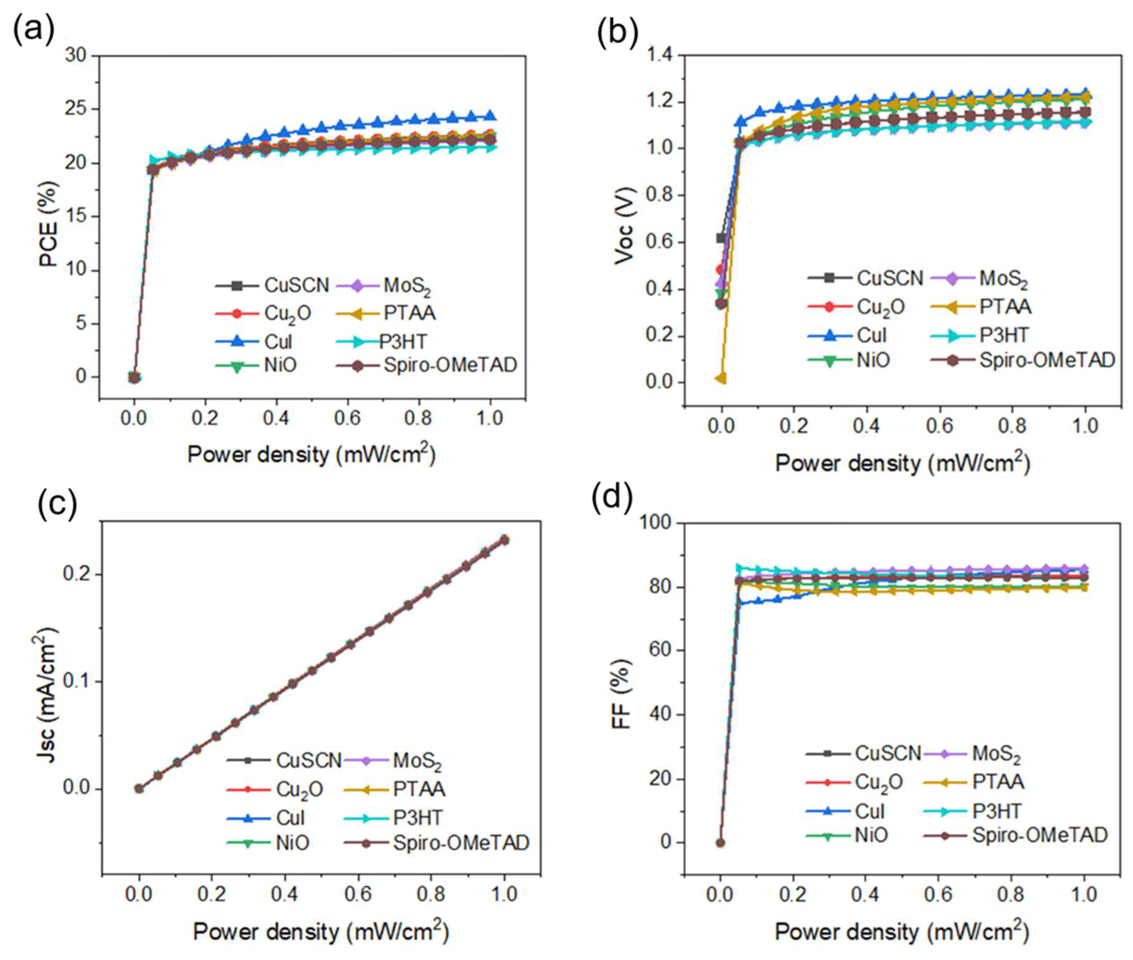
Figure 4.
EQE spectrum of CsPbI₂Br perovskite solar cells with CuI as HTL.
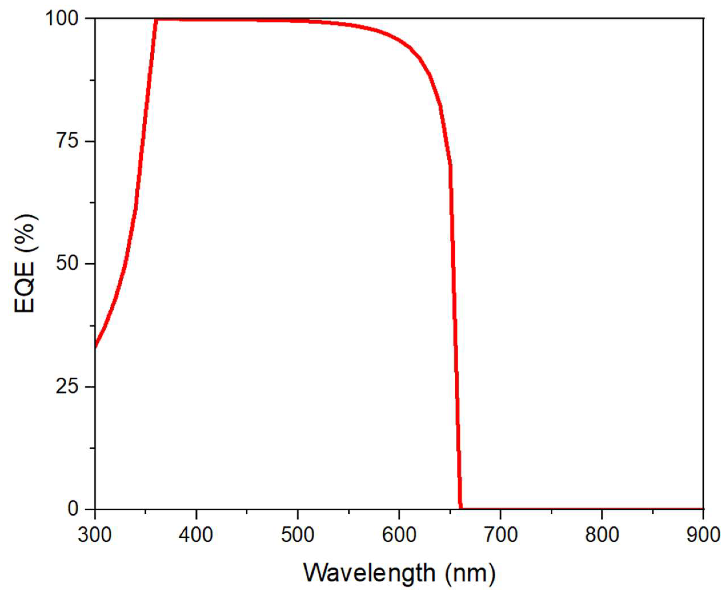
Figure 5.
Effect of HTL (CuI) thickness on solar cell performance parameters: (a) PCE, (b) Voc, (c) Jsc, and (d) FF.
Figure 5.
Effect of HTL (CuI) thickness on solar cell performance parameters: (a) PCE, (b) Voc, (c) Jsc, and (d) FF.
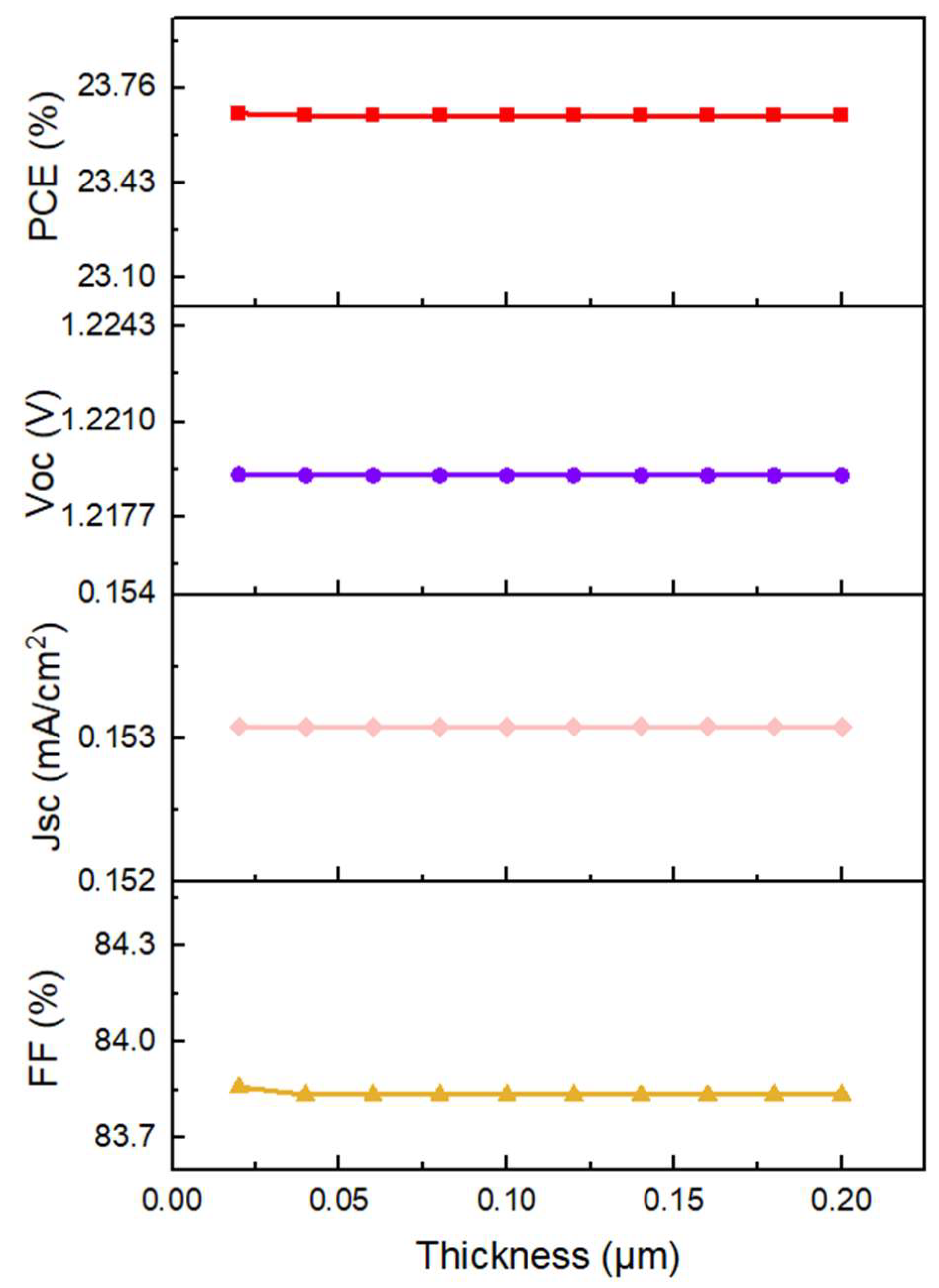
Figure 6.
Influence of absorption layer thickness on performance parameters: (a) PCE, (b) Voc, (c) Jsc, and (d) FF.
Figure 6.
Influence of absorption layer thickness on performance parameters: (a) PCE, (b) Voc, (c) Jsc, and (d) FF.
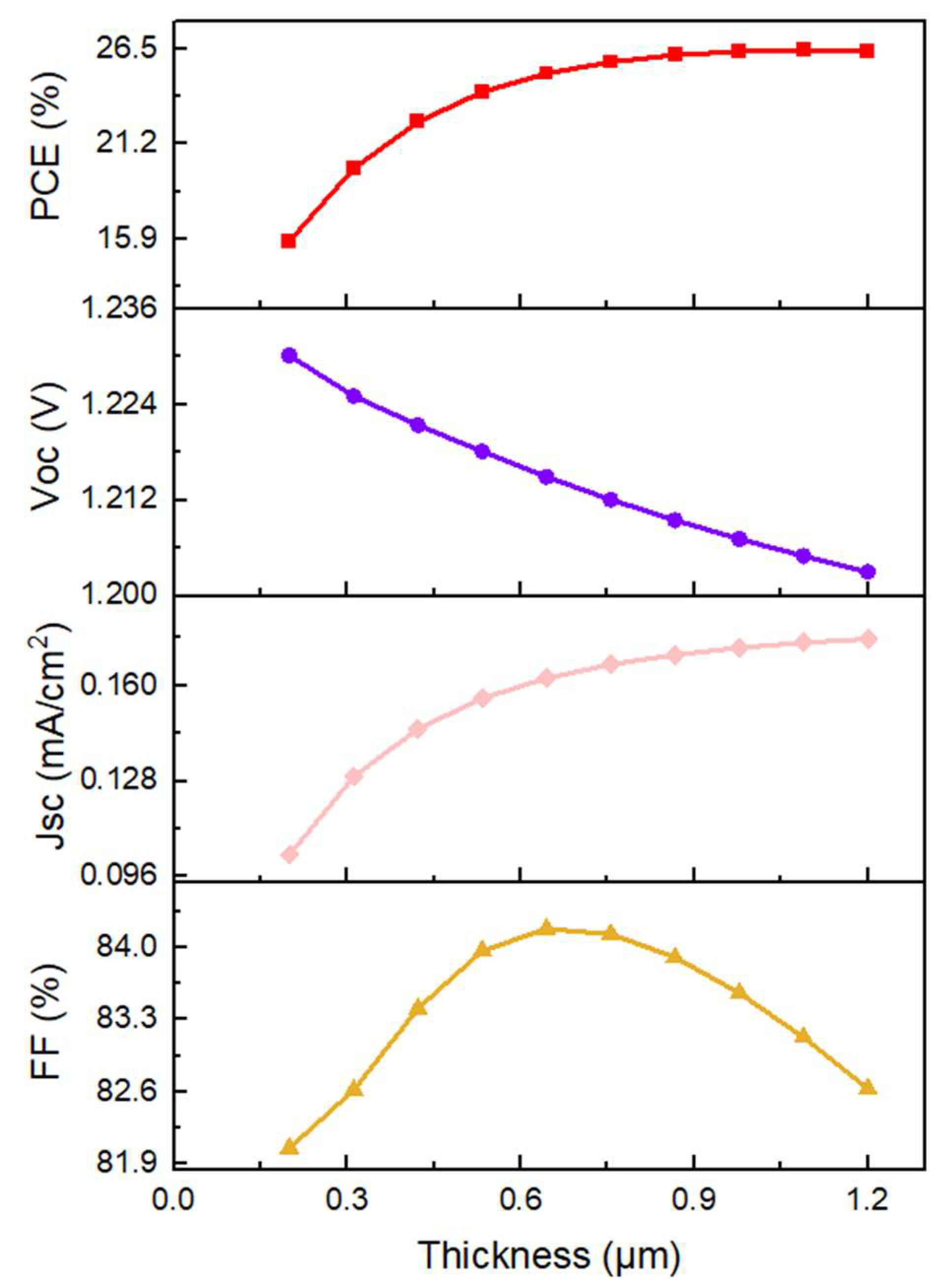
Figure 7.
Impact of CuI's shallow acceptor density on solar cell parameters: (a) PCE, (b) Voc, (c) Jsc, and (d) FF.
Figure 7.
Impact of CuI's shallow acceptor density on solar cell parameters: (a) PCE, (b) Voc, (c) Jsc, and (d) FF.
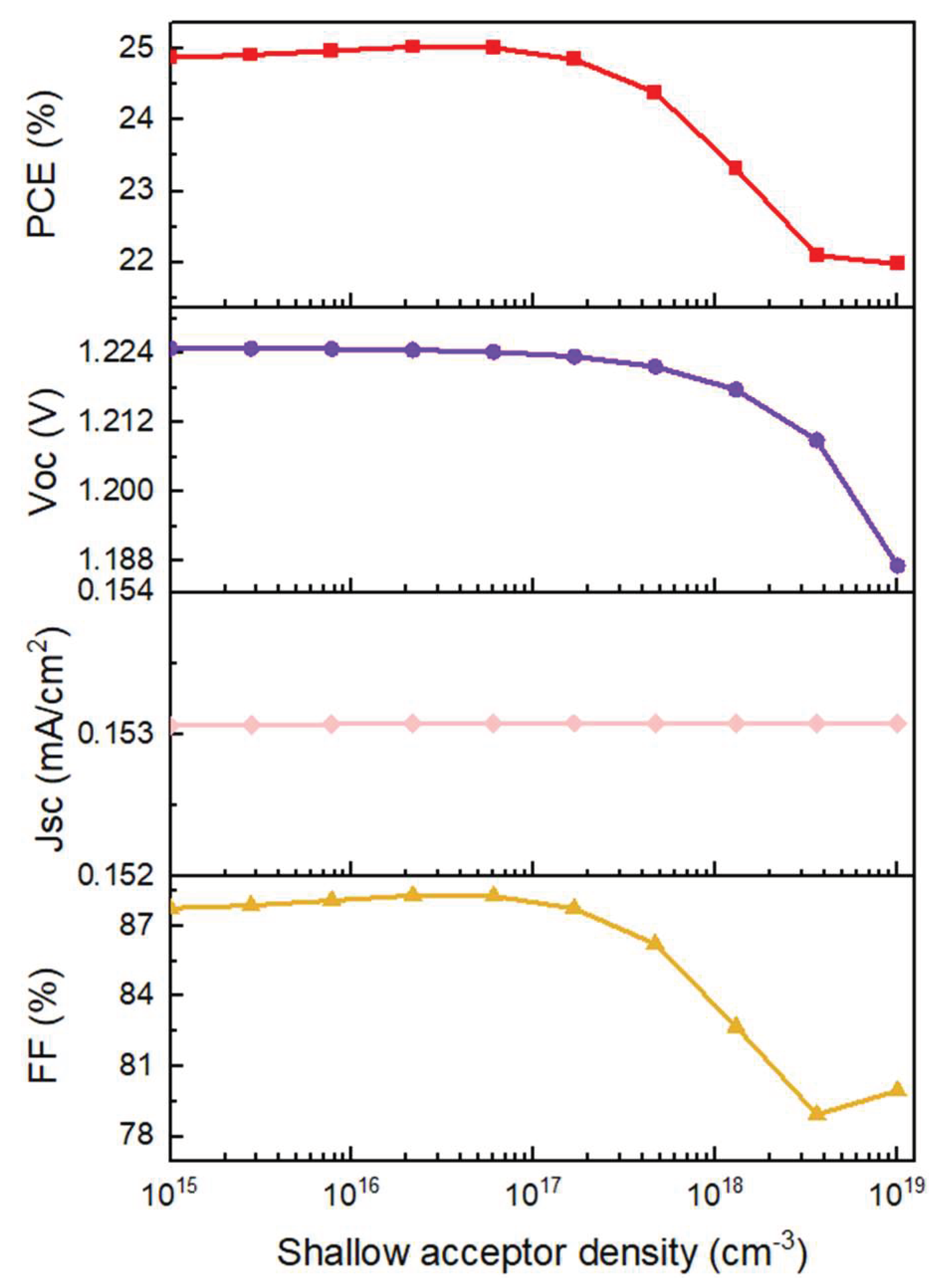
Figure 8.
Effect of absorption layer defect concentration on device performance: (a) PCE, (b) Voc, (c) Jsc, and (d) FF.
Figure 8.
Effect of absorption layer defect concentration on device performance: (a) PCE, (b) Voc, (c) Jsc, and (d) FF.
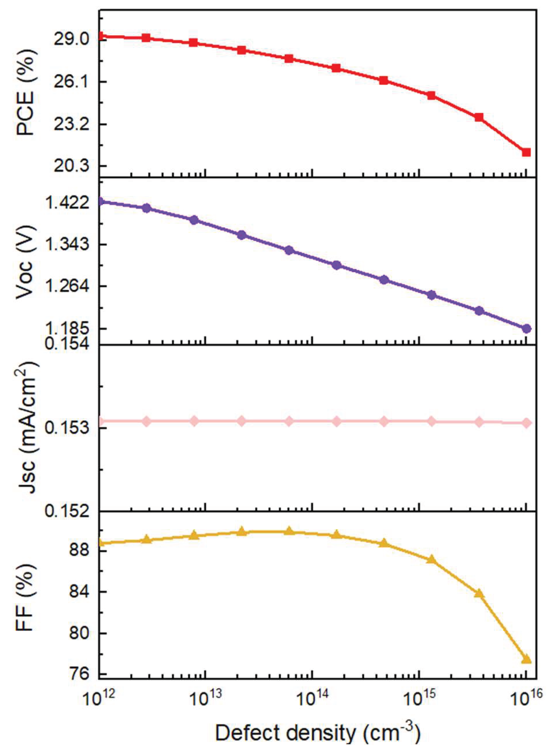
Figure 9.
Influence of interface defect concentration between absorption layer and HTL on device parameters: (a) PCE, (b) Voc, (c) Jsc, and (d) FF.
Figure 9.
Influence of interface defect concentration between absorption layer and HTL on device parameters: (a) PCE, (b) Voc, (c) Jsc, and (d) FF.
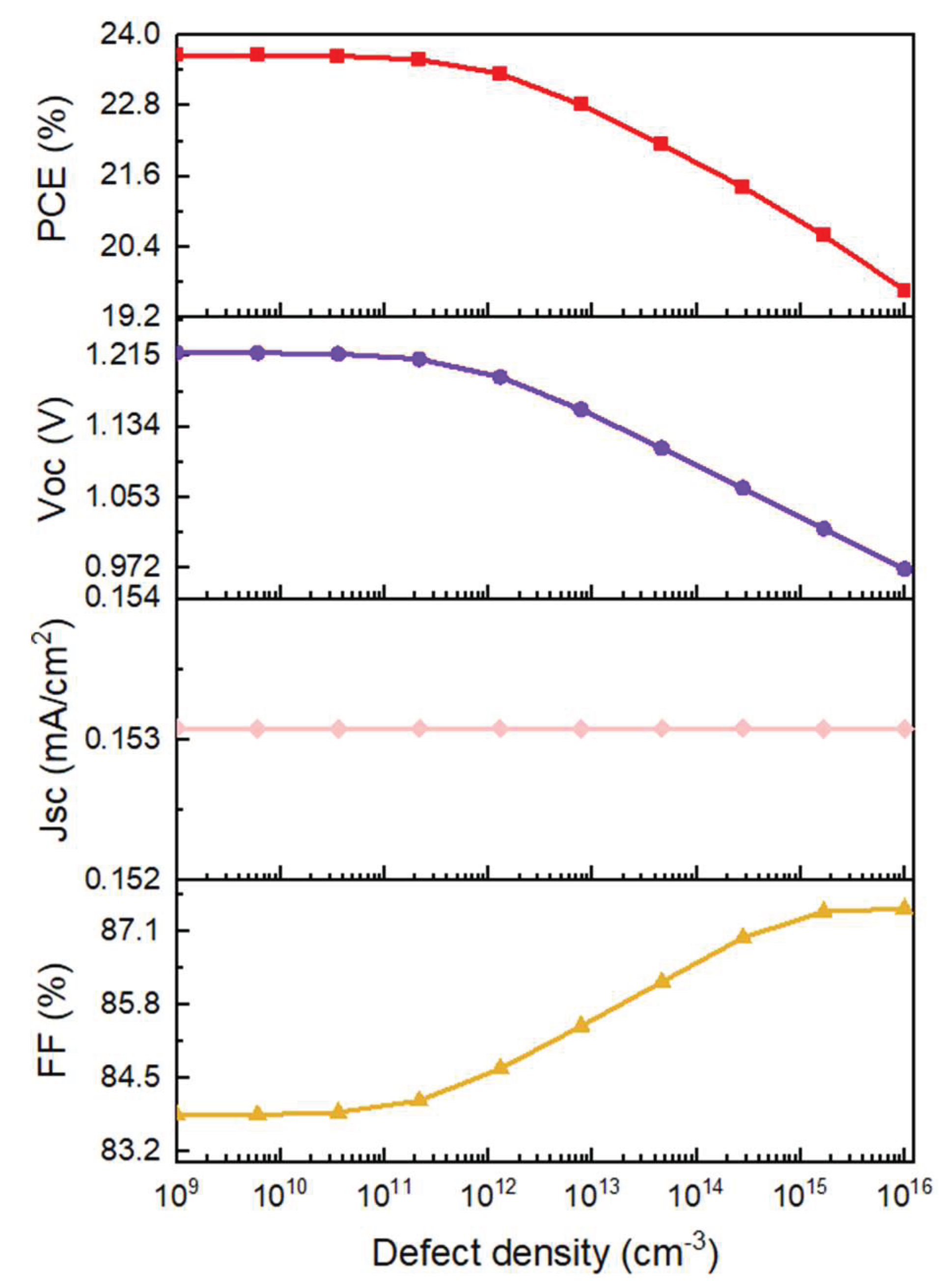
Figure 10.
J-V characteristics of CsPbI₂Br perovskite solar cells with and without HTL under indoor low-light conditions.
Figure 10.
J-V characteristics of CsPbI₂Br perovskite solar cells with and without HTL under indoor low-light conditions.
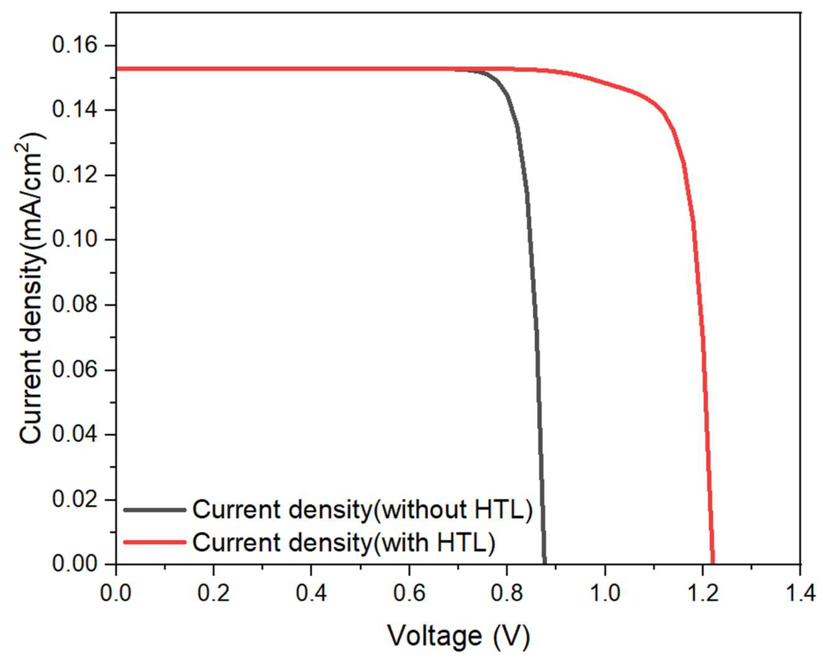

Table 1.
Material parameters for the primary structural layers used in SCAPS-1D simulation [5,20,21].
| Parameters | FTO | SnO2 | CsPbI2Br |
| Thickness (μm) | 0.2 | 0.2 | 0.5 |
| Bandgap (eV) | 3.5 | 3.6 | 1.88 |
| Relative permittivity | 9 | 9 | 8.6 |
| Electron affinity (eV) | 4 | 3.93 | 3.73 |
| Effective DoS at CB (cm⁻³) | 2.2×10¹⁸ | 3.16×10¹⁸ | 1.9×10¹⁸ |
| Effective DoS at VB (cm⁻³) | 1.8×10¹⁹ | 2.5×10¹⁹ | 2.370×10¹⁹ |
| Mob. of electrons (cm²/V·s) | 20 | 20 | 200 |
| Mob. of holes (cm²/V·s) | 10 | 10 | 200 |
| Dop. conc. of acceptor (cm⁻³) | 0 | 0 | 0 |
| Dop. conc. of donor (cm⁻³) | 2.0×10¹⁸ | 1.0×10¹⁸ | 1.0×10¹⁵ |
| Defect density (cm⁻³) | 1.0×10¹⁵ | 1.0×10¹⁵ | 3.64×10¹⁵ |
Table 2.
Physical and electronic properties of various hole transport materials (HTMs) investigated in this study [5,20,21,22].
| Parameters | CuSCN | Cu2O | CuI | NiO | MoS2 | PTAA | P3HT | Spiro-OMeTAD |
|---|---|---|---|---|---|---|---|---|
| Thickness (μm) | 0.2 | 0.2 | 0.2 | 0.2 | 0.2 | 0.2 | 0.2 | 0.2 |
| Bandgap (eV) | 3.6 | 2.17 | 3.1 | 3.8 | 1.29 | 2.96 | 1.85 | 3 |
| Relative permittivity | 10 | 7.1 | 6.5 | 3.8 | 4.26 | 9 | 3.4 | 3 |
| Electron affinity (eV) | 1.7 | 3.2 | 2.1 | 1.46 | 4.2 | 2.3 | 3.1 | 2.45 |
| Effective DoS at CB (cm⁻³) | 2.29×10¹⁹ | 2×10¹⁷ | 2.8×10¹⁹ | 2.8×10¹⁹ | 2.2×10¹⁸ | 2×10¹⁸ | 2×10²⁰ | 2.2×10¹⁸ |
| Effective DoS at VB (cm⁻³) | 1.8×10¹⁸ | 1.1×10¹⁹ | 1×10¹⁹ | 1×10¹⁹ | 1.8×10¹⁹ | 1×10¹⁹ | 2×10²⁰ | 1.9×10¹⁹ |
| Mob. of electrons (cm²/V·s) | 100 | 200 | 100 | 12 | 100 | 1 | 1×10⁻⁴ | 2×10⁻⁴ |
| Mob. of holes (cm²/V·s) | 25 | 80 | 43.9 | 3.8 | 150 | 40 | 1×10⁻³ | 2×10⁻⁴ |
| Dop. conc. of acceptor (cm⁻³) | 1×10¹⁸ | 1×10¹⁸ | 1×10¹⁸ | 1×10¹⁸ | 1×10¹⁸ | 1×10¹⁸ | 1×10¹⁸ | 1×10¹⁸ |
| Defect density (cm⁻³) | 1×10¹⁵ | 1×10¹⁵ | 1×10¹⁵ | 1×10¹⁵ | 1×10¹⁵ | 1×10¹⁵ | 1×10¹⁵ | 1×10¹⁵ |
Table 3.
Interface defect parameters implemented in the SCAPS-1D simulation model [20].
Table 3.
Interface defect parameters implemented in the SCAPS-1D simulation model [20].
| Parameters | SnO2/CsPbI2Br | CsPbI2Br/CuI |
| Defect types | Neutral | Neutral |
| Capture cross section electrons (cm²) | 1.0×10⁻¹⁹ | 1.0×10⁻¹⁹ |
| Capture cross section holes (eV) | 1.0×10⁻¹⁹ | 1.0×10⁻¹⁹ |
| Energy distributions | Single | Single |
| Ref for defect energy level | Above the highest Ev | Above the highest Ev |
| Energy with respect to reference (eV) | 0.6 | 0.6 |
| Total density (cm⁻³) | 1.0×10⁹ | 1.0×10⁹ |
Table 4.
Performance metrics of CsPbI₂Br perovskite solar cells with various HTLs under indoor low-light conditions (white LED, 560 lux, 0.661 mW/cm²).
Table 4.
Performance metrics of CsPbI₂Br perovskite solar cells with various HTLs under indoor low-light conditions (white LED, 560 lux, 0.661 mW/cm²).
| TTLs / Performances | Voc (V) | Jsc (mA/cm2) | FF (%) | PCE (%) |
| CuSCN | 1.1381 | 0.153 | 83.35 | 21.96 |
| Cu2O | 1.1379 | 0.154 | 83.43 | 22.21 |
| CuI | 1.2191 | 0.153 | 83.84 | 23.66 |
| NiO | 1.1891 | 0.153 | 79.85 | 21.98 |
| MoS2 | 1.0908 | 0.152 | 85.63 | 21.57 |
| PTAA | 1.2044 | 0.153 | 79.04 | 22.05 |
| P3HT | 1.1016 | 0.153 | 83.39 | 21.34 |
| Spiro-OMeTAD | 1.1379 | 0.153 | 82.91 | 21.84 |
Table 5.
Performance metrics of CsPbI₂Br perovskite solar cells with various HTLs under reduced indoor illumination (white LED, 0.384 mW/cm²).
Table 5.
Performance metrics of CsPbI₂Br perovskite solar cells with various HTLs under reduced indoor illumination (white LED, 0.384 mW/cm²).
| TTLs / Performances | Voc (V) | Jsc (mA/cm2) | FF (%) | PCE (%) |
| CuSCN | 1.1131 | 0.0889 | 83.04 | 21.4 |
| Cu2O | 1.1132 | 0.0898 | 83.12 | 21.64 |
| CuI | 1.202 | 0.0889 | 81.1 | 22.57 |
| NiO | 1.1521 | 0.0889 | 80.2 | 21.39 |
| MoS2 | 1.0825 | 0.0887 | 84.75 | 21.19 |
| PTAA | 1.1784 | 0.0889 | 78.52 | 21.43 |
| P3HT | 1.0817 | 0.0892 | 84.12 | 21.14 |
| Spiro-OMeTAD | 1.1136 | 0.0889 | 82.82 | 21.35 |
Table 6.
Comparison of simulated optimized CsPbI₂Br perovskite solar cell performance with recent experimental results under standard AM 1.5G solar spectrum (100 mW/cm²).
Table 6.
Comparison of simulated optimized CsPbI₂Br perovskite solar cell performance with recent experimental results under standard AM 1.5G solar spectrum (100 mW/cm²).
| Device structure | Voc (V) | Jsc (mA/cm2) | FF (%) | PCE (%) | Reference |
|---|---|---|---|---|---|
| FTO/SnO₂/CsPbI₂Br/CuI/Au | 1.376 | 16.35 | 86.57 | 19.48 | This work |
| ITO/ZnO/ CsPbI₂Br /P3HT/Au | 1.220 | 14.88 | 75.70 | 13.74 | Bahadur[8] |
| ITO/NiOx/ CsPbI₂Br /PC61BM/BCP/Ag | 1.10 | 15.75 | 75.13 | 13.01 | Chen[23] |
| FTO/TiO2/CsPbI2Br/MoO2-PTAA/Carbon | 1.21 | 15.07 | 80.44 | 14.67 | Lee[24] |
| FTO/TiO2/CsPbI2Br/ Carbon | 1.15 | 13.87 | 64 | 10.21 | Dong[25] |
| FTO/TiO2/CsPbI2Br/Spiro-OMeTAD/Au | 1.21 | 15.67 | 80 | 15.03 | Chen[26] |
Table 7.
Comparison of simulated optimized CsPbI₂Br perovskite solar cell performance with recent experimental results under indoor white LED illumination.
Table 7.
Comparison of simulated optimized CsPbI₂Br perovskite solar cell performance with recent experimental results under indoor white LED illumination.
| Device structure (Illumination intensity) |
Voc (V) | Jsc (mA/cm2) | FF (%) | PCE (%) | Reference |
|---|---|---|---|---|---|
| FTO/SnO₂/CsPbI₂Br/CuI/Au (0.661mW/cm2) |
1.2468 | 0.17043 | 88.90 | 28.57 | This work |
| ITO/SnO2/ZnO/CsPbI₂Br /P3HT/Au (0.382 mW/cm2) |
1.051 | 0.110 | 76.79 | 23.24 | Bahadur[27] |
| ITO/ SnO₂/ CsPbI₂Br / Spiro-OMeTAD/Au (0.3098 mW/cm2) |
0.95 | 0.114 | 70 | 23.51 | Kim[28] |
Disclaimer/Publisher’s Note: The statements, opinions and data contained in all publications are solely those of the individual author(s) and contributor(s) and not of MDPI and/or the editor(s). MDPI and/or the editor(s) disclaim responsibility for any injury to people or property resulting from any ideas, methods, instructions or products referred to in the content. |
© 2025 by the authors. Licensee MDPI, Basel, Switzerland. This article is an open access article distributed under the terms and conditions of the Creative Commons Attribution (CC BY) license (http://creativecommons.org/licenses/by/4.0/).
Copyright: This open access article is published under a Creative Commons CC BY 4.0 license, which permit the free download, distribution, and reuse, provided that the author and preprint are cited in any reuse.


