Submitted:
30 April 2025
Posted:
02 May 2025
You are already at the latest version
Abstract
In this paper, we implement a compact switchable bandpass filter on a 50-ohm microstrip line. The proposed structure comprises an input/output stage with one end terminated at 50 ohm, a C-shaped-open loop resonator, and two L-shaped-open loop resonators. The proposed filter operates in four different modes depending on the on/off combination of the five PIN diodes. Each mode includes a dual-band pass filter (DB-BPF) designed for the 1.4 GHz and 5.1 GHz bands, another DB-BPF covering the 2.4 GHz and 4.2 GHz bands, a wideband BPF with a bandwidth ranging from 2 to 4.5 GHz, and an all-pass filter (APF) that allows all frequencies to pass through. The proposed structure is very small in size because it is implemented on a 50-ohm line without any additional space.
Keywords:
All-pass
; band pass
; dual-band pass
; switchable filter
1. Introduction
Recently, with the development of wireless communication, terminal technology that supports multiple frequency bands simultaneously with a single system is receiving attention. Switchable filters are being presented as an effective alternative in that they can selectively provide multiple modes based on a single structure [1,2]. In particular, switchable filters utilizing PIN diodes are being actively developed because they allow for fast switching speeds and relatively simple circuit configurations.
In [3], a switchable filter with four distinct modes was proposed by integrating a bandstop filter (BSF)/all-stop filter (ASF) structure with a dual-mode resonator (DMR) in a parallel configuration. In [4], three modes of bandpass filter (BPF), BSF, and DB-BPF were implemented based on coupled-lines. In [5], a switchable filter capable of implementing two BPFs and one BSF was proposed, while in [6], a switchable filter designed to implement three modes—BPF, DB-BPF, and BSF—was proposed by combining one main path and an additional path.
In [7], a PIN diode was used to switch between BPF and BSF, and a varactor diode was used to control their resonant frequencies. Similarly, in [8], a structure enabling switching between two modes, BPF and BSF, was proposed, with an absorptive circuit added to enhance the matching characteristics of both modes. However, this structure has the disadvantage of being large in size and having many design parameters because it places multiple structures in parallel and selects one of them using a PIN diode.
To address these issues, research on implementing filter structures directly on 50 Ω microstrip lines has been attracting attention [9]-[12]. In [9], a sext-band BPF was proposed by adding a symmetrical short stub outside the 50-Ω line. In [10], a filter capable of switching between three modes—a broadband filter, a dual-band filter, and a tri-band filter—was implemented by integrating a stub with a PIN diode into the 50-Ω transmission line. However, both studies had the problem of increasing the overall filter size due to the long stub. In [11], a structure capable of switching between BPF and DBPF was proposed using a switchable J-inverter. However, it still had the problem of large size, with a large IL (Insertion Loss) of 2.9–4.9 dB using 13 diodes. In [12], a dual-band notch filter with tunable frequency was implemented by applying an embedded split ring resonator (ESRR) structure loaded with a varactor inside a 50-Ω line. In [13], a simple and compact quadruple-band pass filter was implemented by inserting a C-shaped open-loop resonator inside a 50-Ω line, but the spacing between resonant frequencies is fixed, limiting practical applications. Table 1 presents the performance comparison of previous switchable filters.
In this study, a switchable filter supporting four operation modes including a wideband filter, two DB-BPFs with different operating bands, and an APF is proposed. Unlike previous works, the proposed filter minimizes the size increase by implementing the bias circuit in the empty space inside the proposed structure.
2. Configuration
Figure 1 shows the basic shape of the filter implemented on a simple 50-Ω line. A substrate with a dielectric constant of 2.2 and a thickness of 62 mil is used. The line width at both ends of the basic filter structure is 4.8 mm, which corresponds to a characteristic impedance of 50 Ω. The proposed basic filter consists of a pair of stubs on the top and bottom, two L-shaped resonators, and one C-shaped resonator. The stub has a line width of w and its length of s. The line width of the C-shaped resonator is set to LC, and the line width of the L-shaped resonator is also set to 0.4 mm. The spacing between the stub and the L-shaped resonator, the spacing between the stub and the C-shaped resonator, and the spacing between the 50-ohm line and the L-shaped or C-shaped resonator are set to d.
The basic structure shown in Figure 1 features a total of five gaps, each designated as g, where PIN diodes are applied to enable its function as a switchable filter. Considering that PIN diodes will be applied, all gaps are set to 0.1 mm. Depending on the various on/off combinations of the 5 PIN diodes, the proposed structure operates as a wideband BPF, a narrowband dual-band BPF, and an all-pass filter.
3. Wideband BPF & Dual-band BPF
3.1. Operating Principle
Figure 2 shows four different filter structures and their simulation results according to the applied resonator shape inside the 50-ohm line. Based on these characteristics, a switchable filter will be considered in Section IV. The filter parameters are set as follows: L = 30 mm, s = 14.9 mm, LC = 31.8 mm, w = 0.4 mm, g = 0.1 mm, and d = 0.1 mm.
The structure presented in Figure 1 is Type 3, and the structure with only two L-shaped resonators on the top in Figure 1 is Type 1, and the structure with only one C-shaped resonator on the bottom is Type 2. From the simulation results, it can be seen that Type 1 does not allow RF signals to pass through the entire band, and Type 2 and Type 3 operate identically. From these results, it can be inferred that the two L-shaped resonators on the top are meaningless dummy structures, and the dual-band filter characteristics are implemented by one C-shaped resonator on the bottom. Type 4 is the case where two identical L-shaped resonators are applied on the top and bottom. At this time, the proposed structure exhibits wideband filter characteristics.
3.2. Wideband BPF
Type 4 structure has the same structure at the top and bottom, so it is sufficient to consider only the structure in Figure 3a. As illustrated in Figure 3b, the wideband BPF is constructed using two pairs of coupled transmission lines, each with an electrical length of θ and characteristic impedances Z0o and Z0e for the odd and even modes, respectively. Owing to the filter's symmetrical structure, its behavior can be effectively analyzed through odd- and even-mode techniques, with the corresponding equivalent circuits depicted in Figure 3c and Figure 3d.
The even-mode input impedance of Figure 3c can be expressed by
and the input reflection is
Likewise, the odd-mode input impedance can be obtained
Similarly, the corresponding input reflection is
Therefore, transmission and reflection coefficients of the proposed filter can be obtained as
Figure 4a shows the simulation results of Type 4 (wideband BPF mode) according to the change in stub length s. The parameters for the simulation are the same as those mentioned above. From the simulation results, it can be confirmed that the stub length s affects f2 and the transmission zero (TZ) frequency located on the right side of the passband in the wideband BPF mode. At this time, f1 hardly changed. As the stub length s increases, the right skirt characteristic of the filter improves. In Figure 1, the longest s that can be implemented is 14.9 mm. Considering this fact, the stub length s is selected as 14.9 mm.
Figure 4b shows the electric field distribution at the TZ frequency of 6.57 GHz when s is 14.9 mm. The electric field is stronger as it approaches red and weaker as it approaches blue. In the simulation, the RF signal is set to the left for input and the right for output. Type 4 is a symmetrical structure based on the left and right, and the left and right sides operate as bandstop resonators of one wavelength each. As a result, the S21 of the filter exhibits good characteristics of about −50 dB.
Figure 5 shows the simulation results of the Type 4 structure according to the total filter length L. From the simulation results, it can be seen that L has a significant effect on the first resonant frequency f1, and f1 decreases as L increases.
Figure 6 presents the simulation results of Type 4 by changing the length of one of the two C-shaped resonators. In Fig. 6, we will explain why the proposed structure operates as a wideband filter for Type 4 and a dual-band filter for Type 3. Here, when LC is 31.8 mm, it refers to the Type 4 structure. At this time, the 3-dB operating bandwidth is 1.98–5.18 GHz. The simulation results show that LC gradually decreases and when it reaches 28 mm, two TZs start to appear in the passband of the wideband BPF.
As LC decreases, the frequency of the two TZs increases and becomes more distinct. When the upper C-shaped resonator disappears completely (LC = 0 mm), it becomes the same as Type 2 in Figure 2 and has dual-band filter characteristics. It has already been mentioned above that Type 2 has the same characteristics as Type 3. In this study, the first TZ of the filter is generated by a stub with a length of s, and when a C-shaped resonator is added, the stub and the C-shaped resonator operate as a coupled line. At this time, if the length of the C-shaped resonator is 28 mm or more, the TZ does not appear.
3.3. Dual-band BPF
If the upper one of the two L-shaped resonators is replaced with two C-shaped resonators, the structure in Fig. 1 operates as a dual-band BPF. The dual-band filter has two TZs, one located between the two passbands (f1 and f2) and one located in the upper frequency band of the upper passband (f2). The corresponding frequencies are referred to as fTZ1 and fTZ2, respectively. Figure 7 shows the simulation results of Type 3 as the stub length s changes. As s increases, fTZ1 decreases. At this time, fTZ2, which exists on the right side of f2, shows a tendency to decrease slightly.
Figure 8a,b show the E-field distribution formed at the transmission zero frequency, respectively. As can be seen from the field distribution, the stubs are operating as λ/4 resonators and λ resonators, respectively. The field distribution shown in Figure 7b is identical to that in Figure 4b. When operating in dual-band filter mode, the second TZ is identical to the right TZ in the wideband filter mode.
Figure 9 shows the simulated S21 response of the Type 3 structure as the length LC changes. According to the simulation results, as the length of LC decreases, f2 shifts significantly to higher frequencies, and f1 also increases, but the change is relatively small. This indicates that the change in the length LC of the C-shaped resonator is more sensitive to the higher resonant frequency f2.
Figure 10 shows the electric field distribution at two resonant frequencies f1 and f2 of Type 3 with dual-band BPF characteristics. The parameter settings for the simulation are as follows: L = 30 mm, s = 14.9 mm, LC = 32.7 mm, g = 0.1 mm. As shown in the figure, in the case of Type 3, the RF signal is well transmitted along the lower path at both resonant frequencies. On the other hand, a strong electric field is formed between the gaps in the upper path, and the electric field cannot pass from left to right. At f1, one null exists in the center, and at f2, two nulls exist, operating at half-wavelength and one-wavelength, respectively.
Figure 11 shows the S21 simulation results of the Type 3 structure according to the change in length L. The length L is a parameter that affects both the main resonant frequencies f1 and f2. According to the simulation results, as the length of L increases, the two resonant frequencies f1 and f2 shift to lower frequencies, respectively. This occurs because an increase in length L extends the structure's effective electrical length, thereby lowering the resonant frequency.
4. Switchable Filter Design with Bais Circuit
Figure 12 (a) shows a switchable filter with five diodes and a bias circuit to operate them. The configuration of the switchable filter is the same as Figure 1 except for the bias circuit and diodes. The two D2s located on the left and right gaps and the two D3s located on the upper and lower outer gaps are each configured as a pair. The bias circuit consists of an inductor (green), a capacitor (blue), and a resistor (black). As is well known, the thinner and shorter the bias line, the better. Accordingly, the line width was set to 0.1 mm and the length to 5.6 mm. To implement the bias circuit in a limited space, the capacitor is located on the back side where the GND is located. Li1 = 3, Li2 = 1mm are set, and other parameters are maintained as optimized values obtained based on the parameter study performed in Section III. Figure 12b shows the equivalent circuit of the diode used. It acts as a resistor in the On state and as a capacitor in the Off state. Ron is 5.2 ohm, Coff is 0.025 pF, and LS is about 0.5 nH.
When simulating the switchable filter including the bias circuit, the equivalent values of the diode are all considered. The bias voltages used to control the On/Off state of each diode are shown in Table 2. In the case of D3, the bias voltage is applied by connecting a bias tee to the ports at both ends of the line. The voltages applied to the bias tees are indicated as V4 and V5 in Figure 12a, respectively. Figure 12c shows the fabricated switchable filter.
Figure 13 shows the simulated filter characteristics when the values of R and L used in the bias circuit are changed. The values of R and L used in the bias circuit have a large effect when the proposed structure operates as a dual-band filter, but have a relatively small effect when it operates as a wideband filter. For this reason, only simulation results applying the bias circuit to the dual-band filter are presented in this paper. As the inductor value increases, the insertion loss in the 1.5 GHz band, which is f1, tends to decrease. At this time, the insertion loss in the 5.5 GHz band, which is f2, showed almost no change. Since the inductor has a large impedance value as the frequency increases, the impedance is relatively large in the f2 band, which is a relatively high frequency. Accordingly, the RF signal flowing through the bias circuit can be appropriately blocked. On the other hand, the impedance is relatively small in the f1 band, so some RF signals flow into the bias circuit. This is because the insertion loss in f1 improves as the inductor value increases.
However, when the inductor value is 90 nH, S21 ripple is formed in the f2 band. Among the three inductors, the insertion loss could be reduced by lowering the inductor value of the V2 section to 68 nH. When no resistor is used in the bias circuit, the insertion loss is the smallest in the 1.5 GHz band, but resonance occurred at 0.6 GHz and strong ripple occurred in the 5.5 GHz band. When a 0.3 Kohm resistor is used, the insertion loss in the f1 band decreases, but the insertion loss in the f2 band increases.
Figure 14 shows the electric field distribution when the inductor values used in the bias circuit are 29 nH and 90 nH/68 nH, respectively. At this time, the simulation is performed at f1. In the case of 29 nH, it can be confirmed from the simulation results that the electric field is also formed in the bias circuit. On the other hand, when 68 and 90 nH are mixed, there is almost no electric field formed in the bias circuit. Based on these facts, it can be confirmed that the small inductor value is not sufficient to operate as an RF chock to prevent the electric field from passing through to the bias circuit.
Figure 15 shows the simulation results of the effect of the bias circuit applied position Li1 on the filter performance. As the bias applied position changes, there is little effect in other modes, but the effect is very strong in the BSF mode where the D2 diode is turned on. From the simulation results, as Li1 increases, the insertion loss of S21 tends to decrease in both resonant frequency bands. However, when Li1 is 5 mm, there is a problem of S21 ripple occurring in the 5.5 GHz band. Considering these facts, Li1 is selected as 3 mm.
The switchable filter operates as two types of dual-band BPF, wideband BPF, and all-pass filter depending on various bias combinations. The simulation and measurement results for these four cases are presented in Figure 16. It is confirmed that some measured TZ occurred at a slightly lower frequency than the simulation. This is because of the error that occurred during the fabrication of the designed structure and the inaccuracy of the equivalent model of the PIN diode applied to the simulation at high frequencies. Considering this fact, the simulation and measurement results can be seen to be in good agreement overall. When D1 is off, D2 is on, and D3 is off, the switchable filter operates as a DB-BPF, and the results are presented in Figure 16a. The measured 3-dB fractional bandwidths centered at f1 = 1.4 and f2 = 5.1GHz are 23.49 and 14.42%, respectively. The measured insertion losses at this time are −1.33 and −1.3 dB, respectively. On the other hand, when D1 is off, D2 is off, and D3 is off, the switchable filter operates as a DB-BPF, and the operating bandwidths are f1 = 2.4 and f2 = 4.2GHz, respectively, and the measured 3-dB fractional operating bandwidths are 23.33 and 13.27%. The insertion losses are −0.88 and −2.04 dB, respectively. Figure 16c shows the result when the switchable filter operates as a wideband BPF. At this time, the bias conditions are D1 on, D2 off, and D3 off. The measured 3-dB fractional bandwidth is 73.36% (2.05–4.41 GHz) and the insertion loss is −0.69 dB. Figure 16d shows the result when operating as an APF. At this time, the bias conditions are D1, D2 don’t care, and D3 on. The measurement results show that the APF exhibits an insertion loss of −2.34 dB in the entire operating frequency range of 0–7 GHz, confirming that signal transmission is efficient.
5. Conclusions
In this paper, a compact switchable filter supporting four modes is designed and implemented. The proposed filter provides DB-BPF centered at 1.4 GHz/5.1 GHz and 2.4 GHz/4.2 GHz, a wideband BPF from 2.05 to 4.41 GHz, and an APF operating from 0 to 7 GHz. The bias circuit is integrated into the 50-Ω line to improve space efficiency, and the simulation and measurement results are generally in good agreement. In particular, the proposed filter satisfies the miniaturization and multifunctionality required for next-generation communication systems such as 5G and IoT, and demonstrates excellent performance
6. Patents
A patent application based on the work presented in this manuscript is currently under preparation but has not yet been submitted.
Author Contributions
Conceptualization, Y.S.; validation, Y.C.; visualization, Y.C.; supervision, Y.S.; Investigation, Y.C.; Formal analysis, Y.C., Y.S and J.K. All authors have read and agreed to the published version of the manuscript
Funding
This work was supported in part by the Technology Innovation Program under Grant 20017411, Development of Gen.10 OLED Evaporation Core modules for TV, funded by the Ministry of Trade, Industry and Energy (MOTIE, Korea)
Institutional Review Board Statement
Not applicable.
Informed Consent Statement
Not applicable.
Data Availability Statement
The data that support the findings of this study are available from thecorresponding author upon reasonable request.
Conflicts of Interest
The authors declare no conflict of interest.
References
- Tang, C.-W. Design of a switchable microstrip bandpass filter with single- and dual-band functionality. In Proceedings of the 2024 IEEE International Symposium on Radio-Frequency Integration Technology (RFIT), Chengdu, China, 11–13 September 2024. [Google Scholar] [CrossRef]
- Mu, R.; Wu, Y.; Pan, L.; Zhao, W.; Wang, W. A miniaturized low-loss switchable single- and dual-band bandpass filter. Int. J. RF Microw. Comput.-Aided Eng. 2023, 2023, 9025980. [Google Scholar] [CrossRef]
- Xu, J. A microstrip switchable filter with four operating modes. IEEE Microw. Wirel. Compon. Lett. 2016, 26, 101–103. [Google Scholar] [CrossRef]
- Li, D.; Xu, K.-D. Multifunctional switchable filter using coupled-line structure. IEEE Microw. Wirel. Compon. Lett. 2021, 31, 457–460. [Google Scholar] [CrossRef]
- Feng, W.; Shang, Y.; Che, W.; Gómez-García, R.; Xue, Q. Multifunctional reconfigurable filter using transversal signal-interaction concepts. IEEE Microw. Wirel. Compon. Lett. 2017, 27, 980–982. [Google Scholar] [CrossRef]
- Deng, X.; Dong, G.; Xu, K.-D. Compact switchable filter with three state modes using simple microstrip structure. Microw. Opt. Technol. Lett. 2022, 64, 1162–1169. [Google Scholar] [CrossRef]
- Chen, F.-C.; Li, R.-S.; Chen, J.-P. A tunable dual-band bandpass-to-bandstop filter using p-i-n diodes and varactors. IEEE Access 2018, 6, 46058–46065. [Google Scholar] [CrossRef]
- Wu, G.; Wu, H.; Qin, W.; Shi, J.; Zhang, W.; Lin, L.; Li, Q. Design of a switchable filter for reflectionless-bandpass-to-reflectionless-bandstop responses. Micromachines 2023, 14, 424. [Google Scholar] [CrossRef] [PubMed]
- Luo, J.; Liu, Z.; Gao, S. Design of novel multiband bandpass filters based on coupled symmetric short-circuit stub multimode resonators. Electron. Lett. 2024, 60, e70049. [Google Scholar] [CrossRef]
- Sun, Z.; Wang, X.; Li, K. A switchable bandpass filter for broadband, dual-band and tri-band operations. IEEE Trans. Circuits Syst. II: Exp. Briefs 2023, 70, 111–115. [Google Scholar] [CrossRef]
- Cho, Y.-H.; Park, C.; Yun, S.-W. 0.7–1.0-GHz switchable dual-/single-band tunable bandpass filter using a switchable J-inverter. IEEE Access 2021, 9, 16967–16974. [Google Scholar] [CrossRef]
- Farzami, F.; Khaledian, S.; Stutts, A.C.; Smida, B.; Erricolo, D. Embedded split ring resonator tunable notch band filter in microstrip transmission lines. IEEE Access 2022, 10, 37294–37304. [Google Scholar] [CrossRef]
- Sung, Y. Simple quad-band bandpass filter implemented on a 50-Ω microstrip line. Microw. Opt. Technol. Lett. 2020, 62, 100–107. [Google Scholar] [CrossRef]
Figure 1.
Basic filter implemented on a simple 50-ohm line.
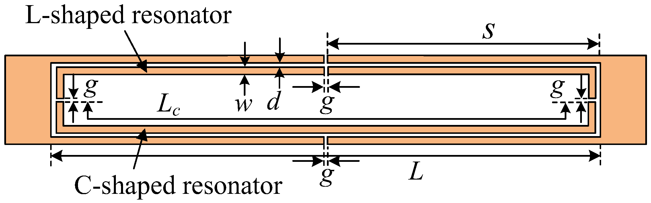
Figure 2.
(a) Various filter structures and (b) their corresponding simulation results.
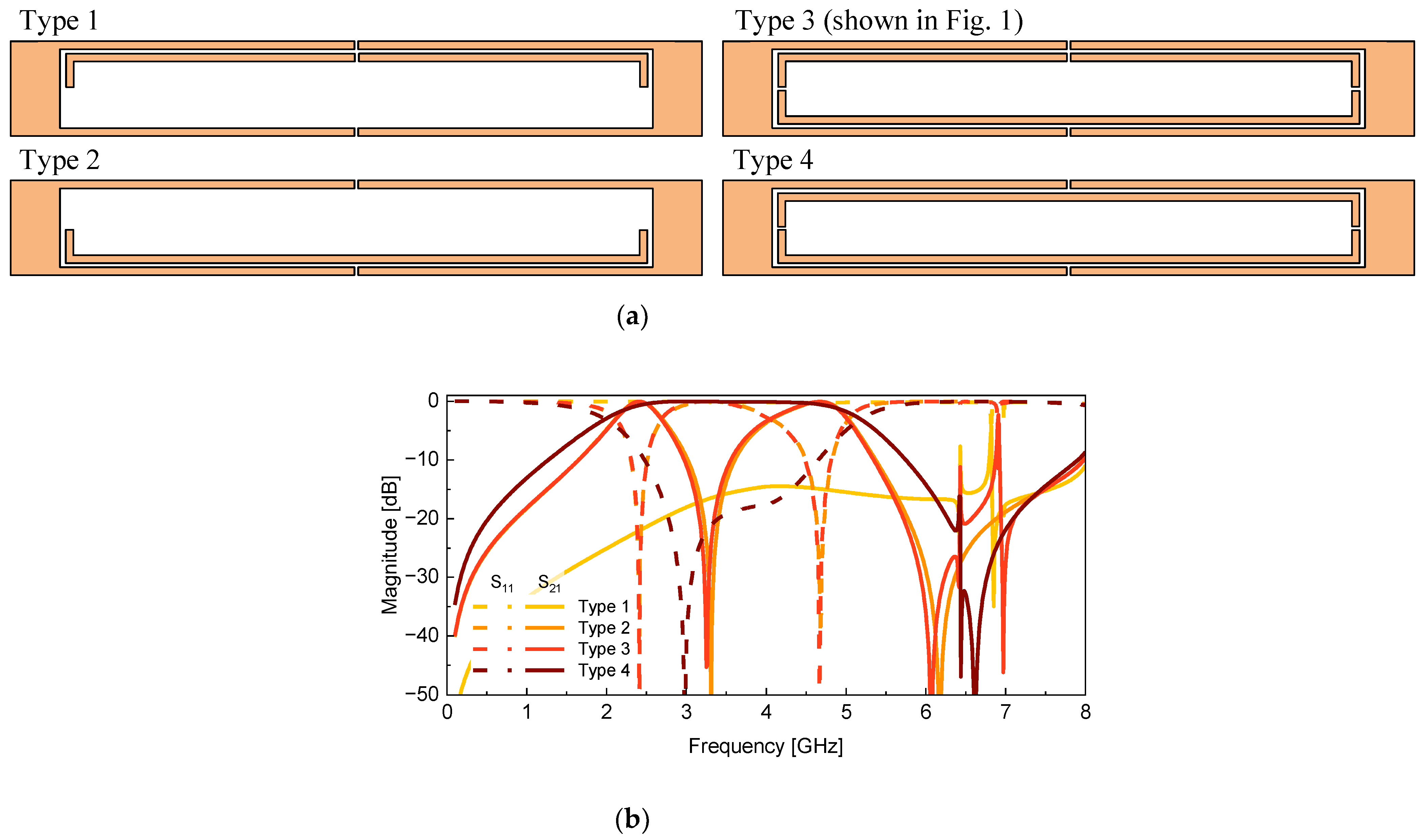
Figure 3.
Wideband bandpass filter. (a) layout. (b) Transmission line model. (c) even-mode equivalent circuit. (d) odd-mode equivalent circuit.
Figure 3.
Wideband bandpass filter. (a) layout. (b) Transmission line model. (c) even-mode equivalent circuit. (d) odd-mode equivalent circuit.
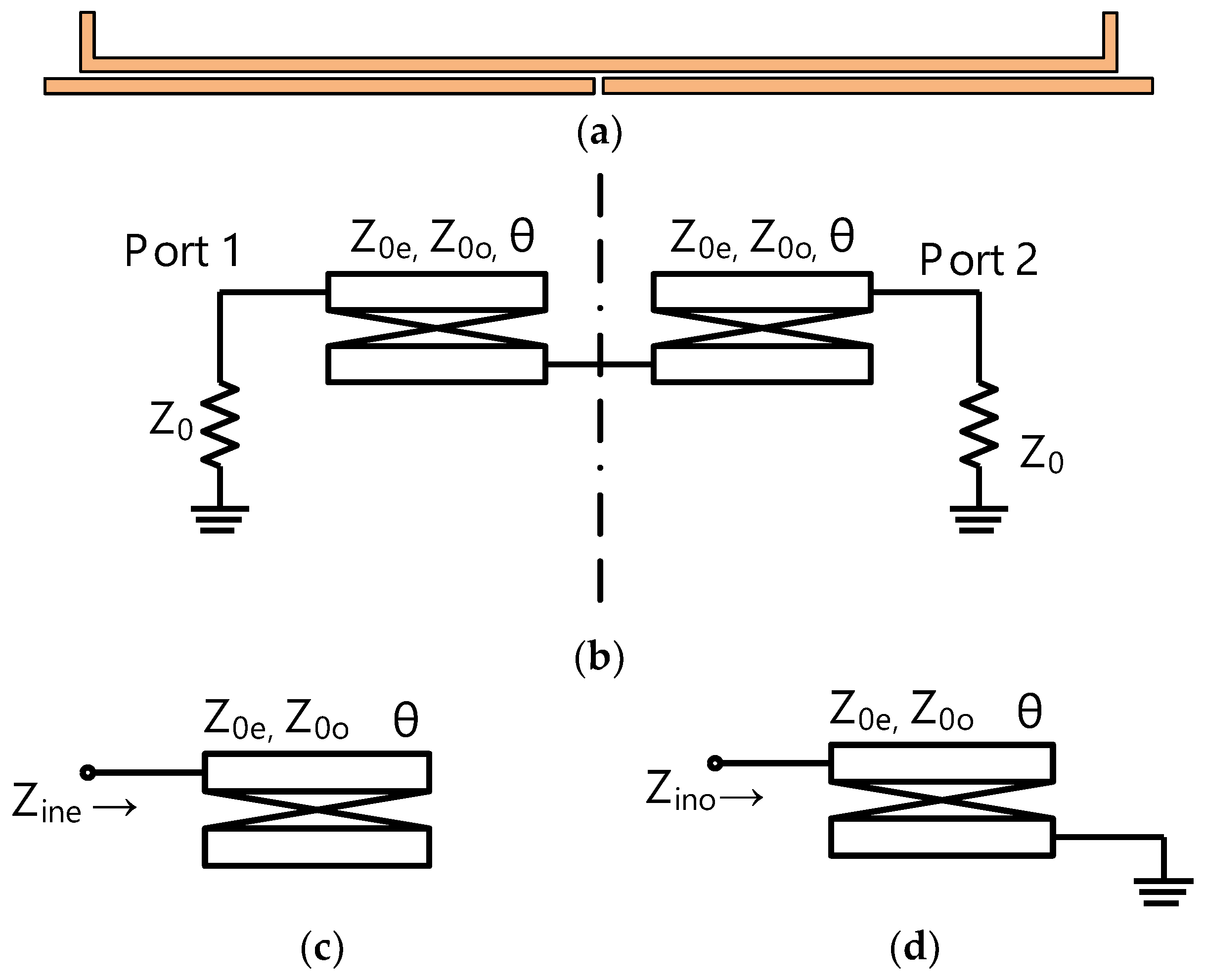
Figure 4.
(a) Simulation results of type 4 according to stub length s. (b) E-field distribution at the transmission zero frequency.
Figure 4.
(a) Simulation results of type 4 according to stub length s. (b) E-field distribution at the transmission zero frequency.
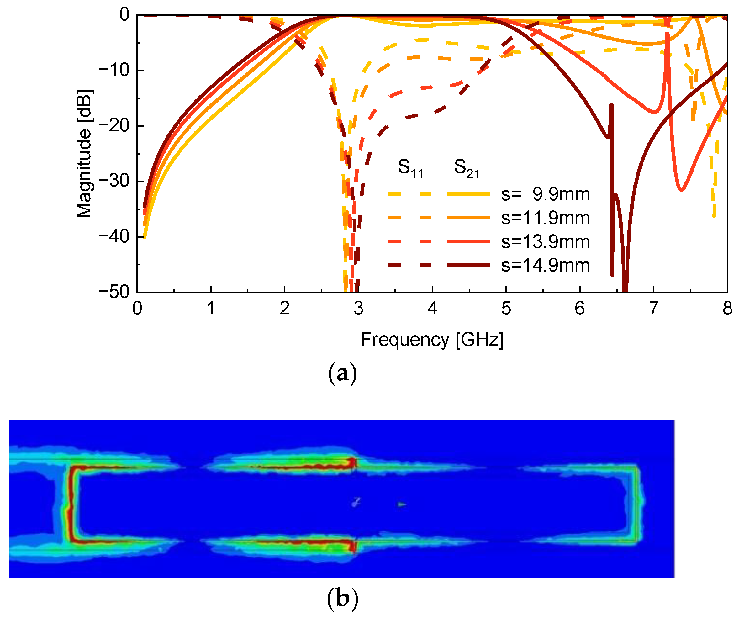
Figure 5.
Simulation results of Type 4 according to length L.
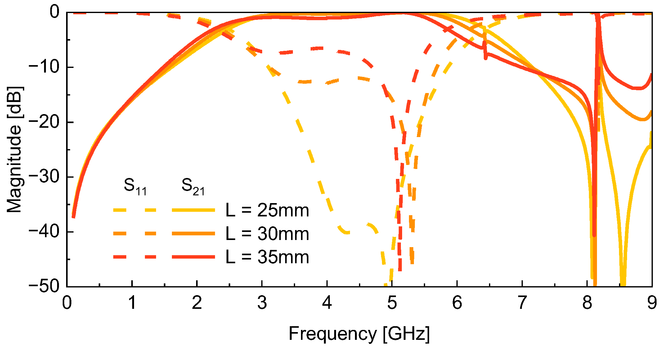
Figure 6.
Simulation results of Type 4 according to LC length. (a) S11 (b) S21.
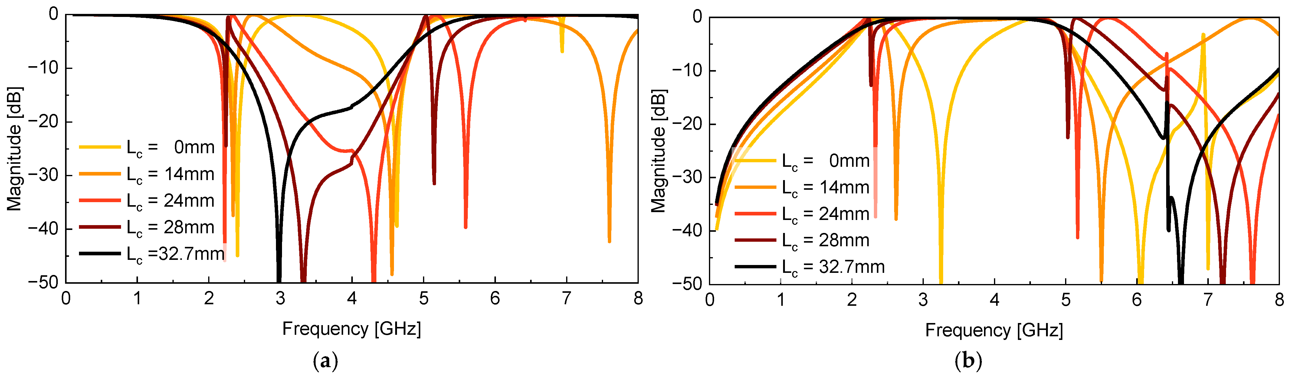
Figure 7.
Simulation results of Type 3 according to length s.
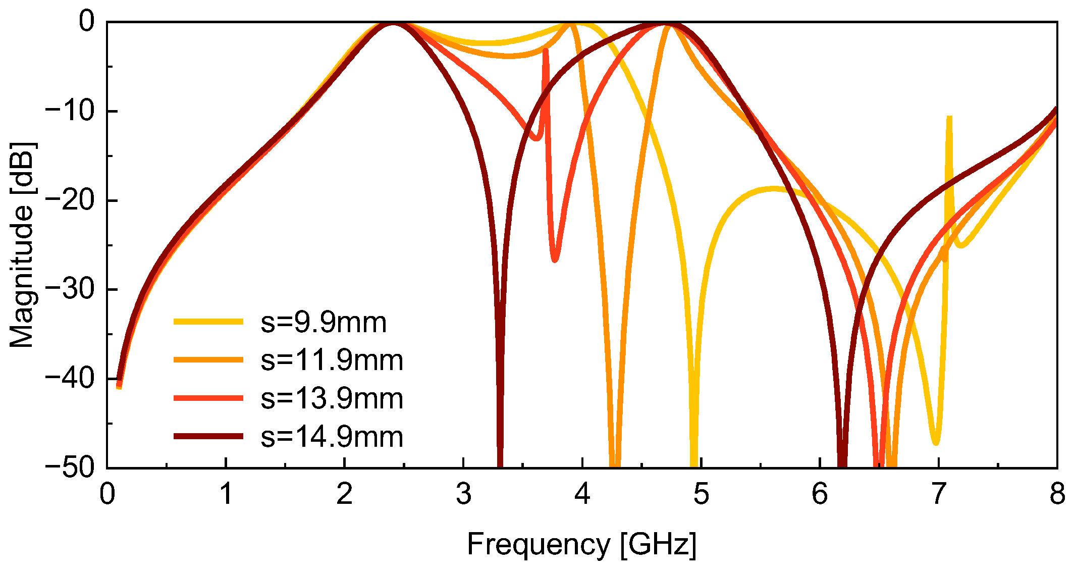
Figure 8.
E-field distribution at (a) fTZ1 and (b) fTZ2.
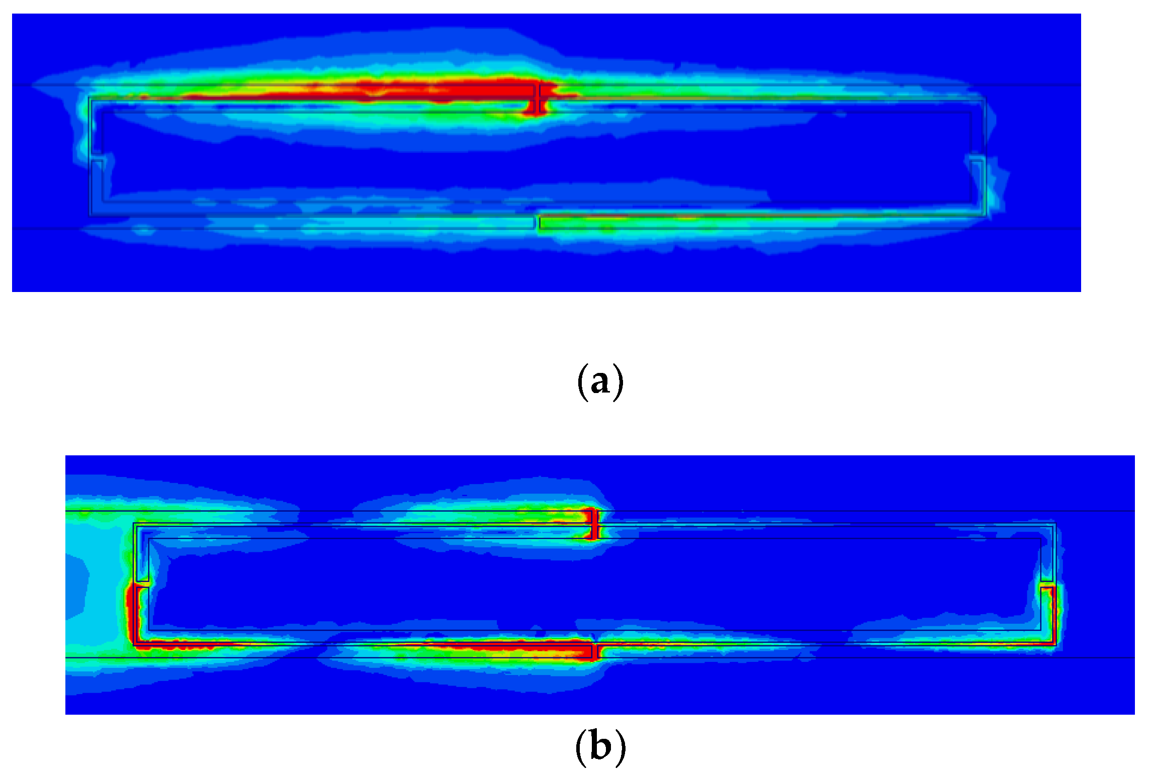
Figure 9.
Simulation results of type 3 according to the length LC of the C-shaped resonator.
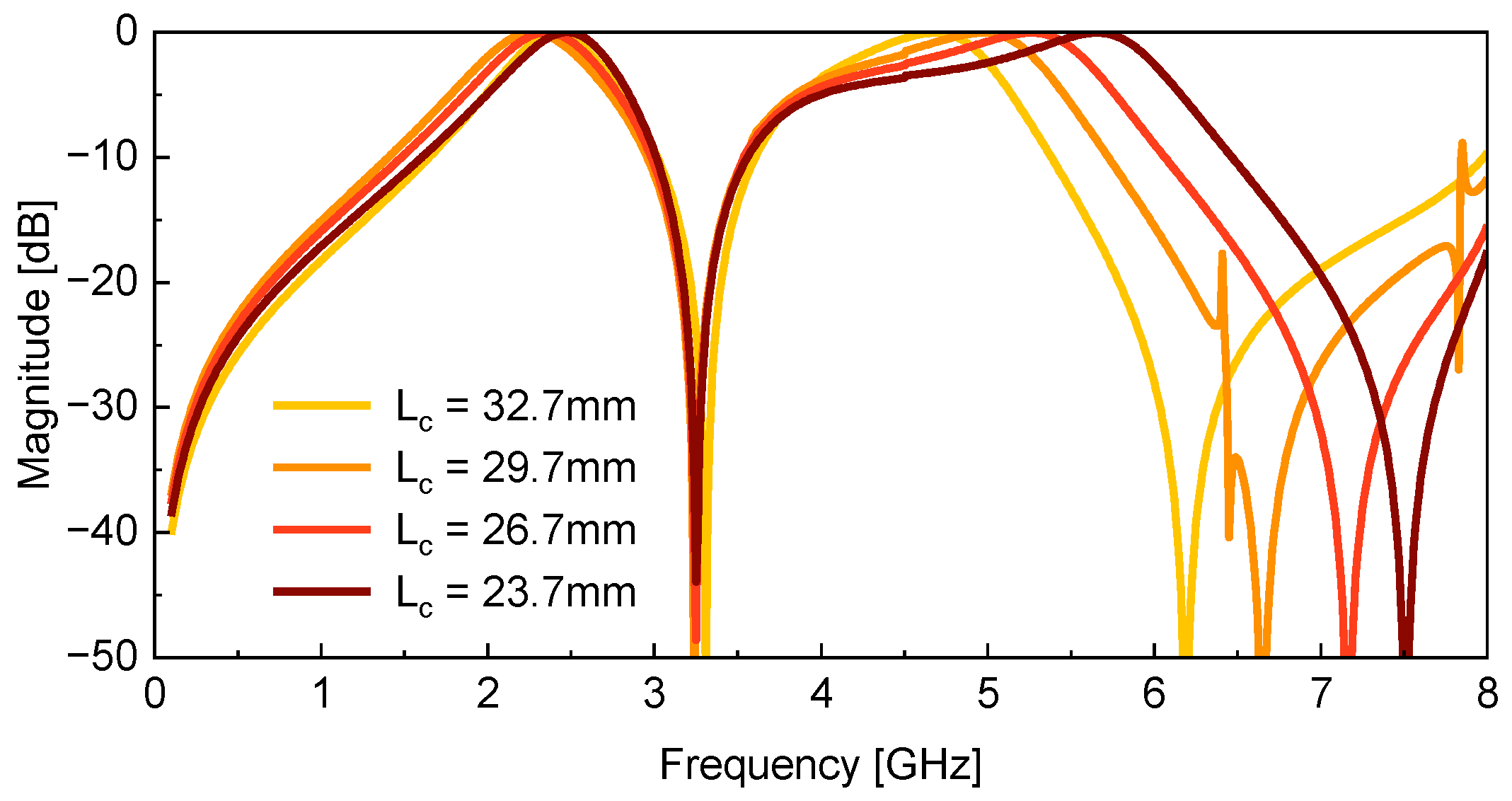
Figure 10.
E-field distribution (a) f1=3 GHz (b) f2=5GHz.
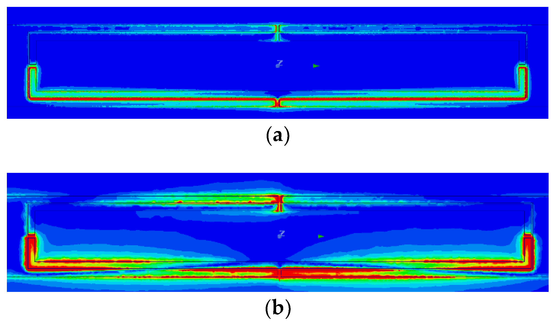
Figure 11.
Simulation results of Type 3 according to the change in length L.
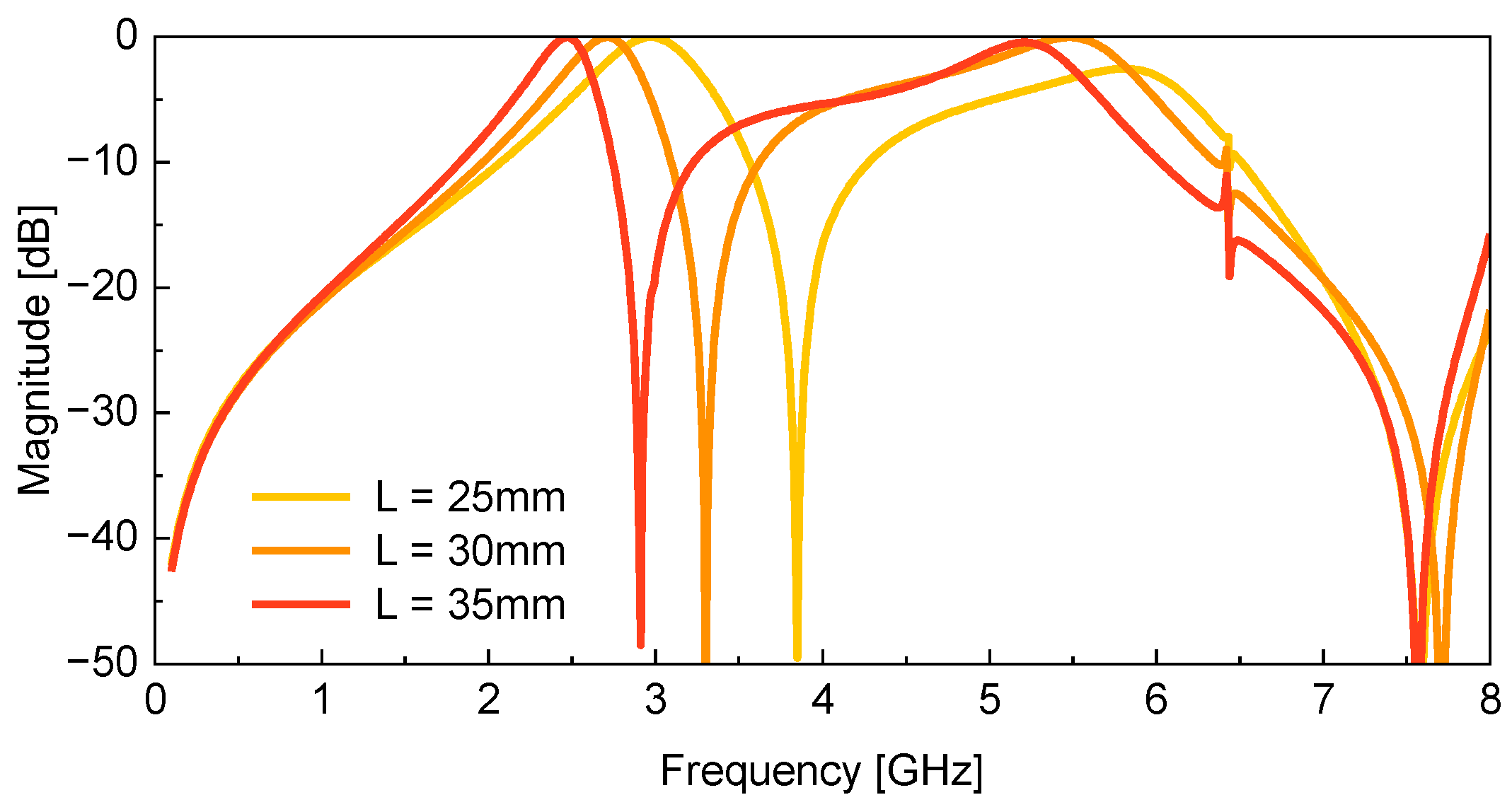
Figure 12.
(a) Proposed filter with bias circuit included (b) Equivalent circuit of the MADP-000907-14020 PIN diode used (c) Photograph of the fabricated switchable filter.
Figure 12.
(a) Proposed filter with bias circuit included (b) Equivalent circuit of the MADP-000907-14020 PIN diode used (c) Photograph of the fabricated switchable filter.
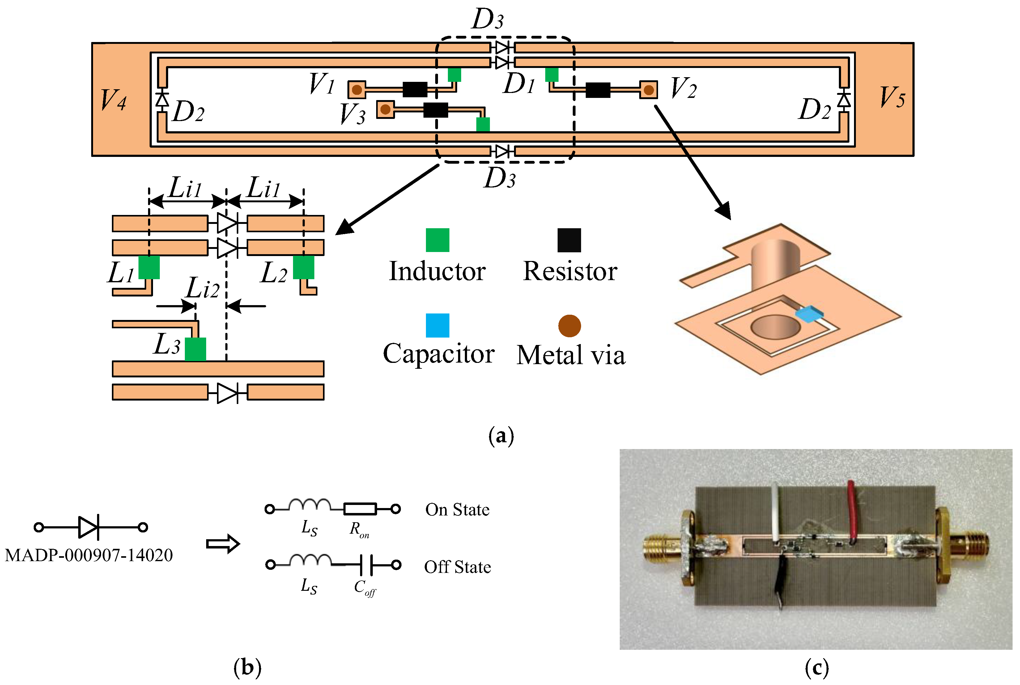
Figure 13.
Simulation results of switchable filter according to the values of resistors and inductors used in the bias circuit. (a) S11. (b) S21.
Figure 13.
Simulation results of switchable filter according to the values of resistors and inductors used in the bias circuit. (a) S11. (b) S21.
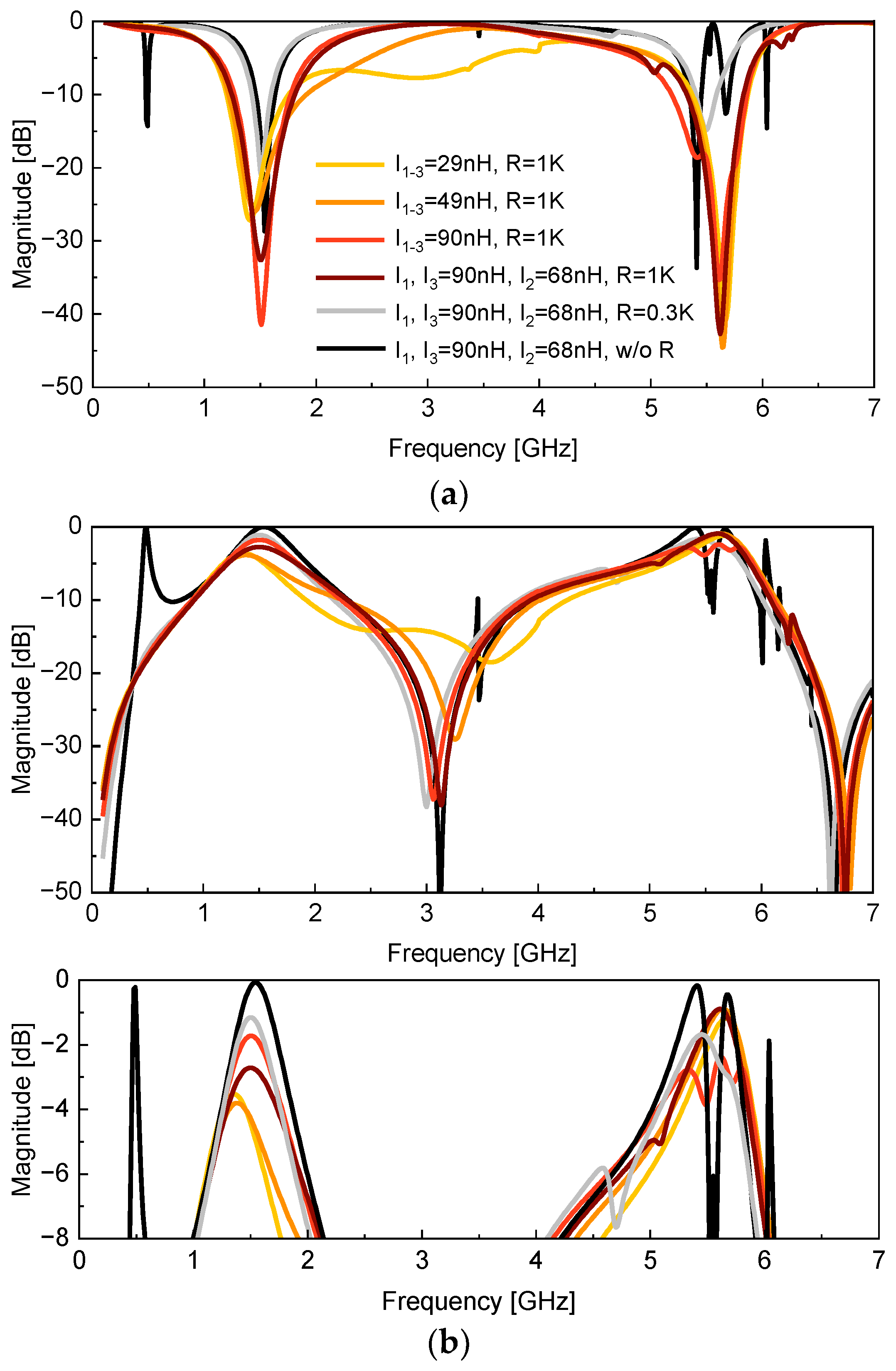
Figure 14.
E-field distribution at f1 when the inductor is (a) 29nH (b) 90nH and 68nH.
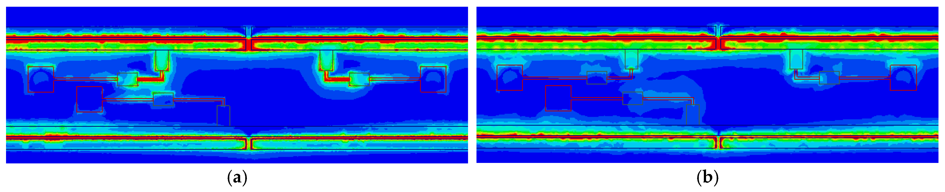
Figure 15.
Simulated filter performance with different bias positions Li1.
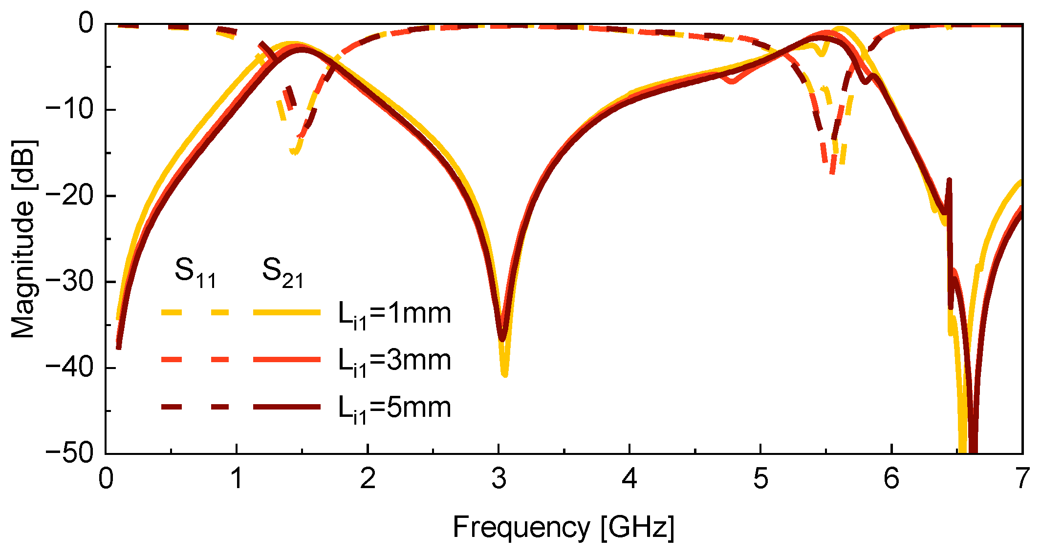
Figure 16.
Simulated and measured results. (a) dual-band filter (D1: off, D2: on, D3: off) (b) dual-band filter (D1: off, D2: off, D3: off) (c) wideband filter (D1: on, D2: off, D3: off) (d) all pass filter (D1: don’t care, D2: don’t care, D3: on).
Figure 16.
Simulated and measured results. (a) dual-band filter (D1: off, D2: on, D3: off) (b) dual-band filter (D1: off, D2: off, D3: off) (c) wideband filter (D1: on, D2: off, D3: off) (d) all pass filter (D1: don’t care, D2: don’t care, D3: on).
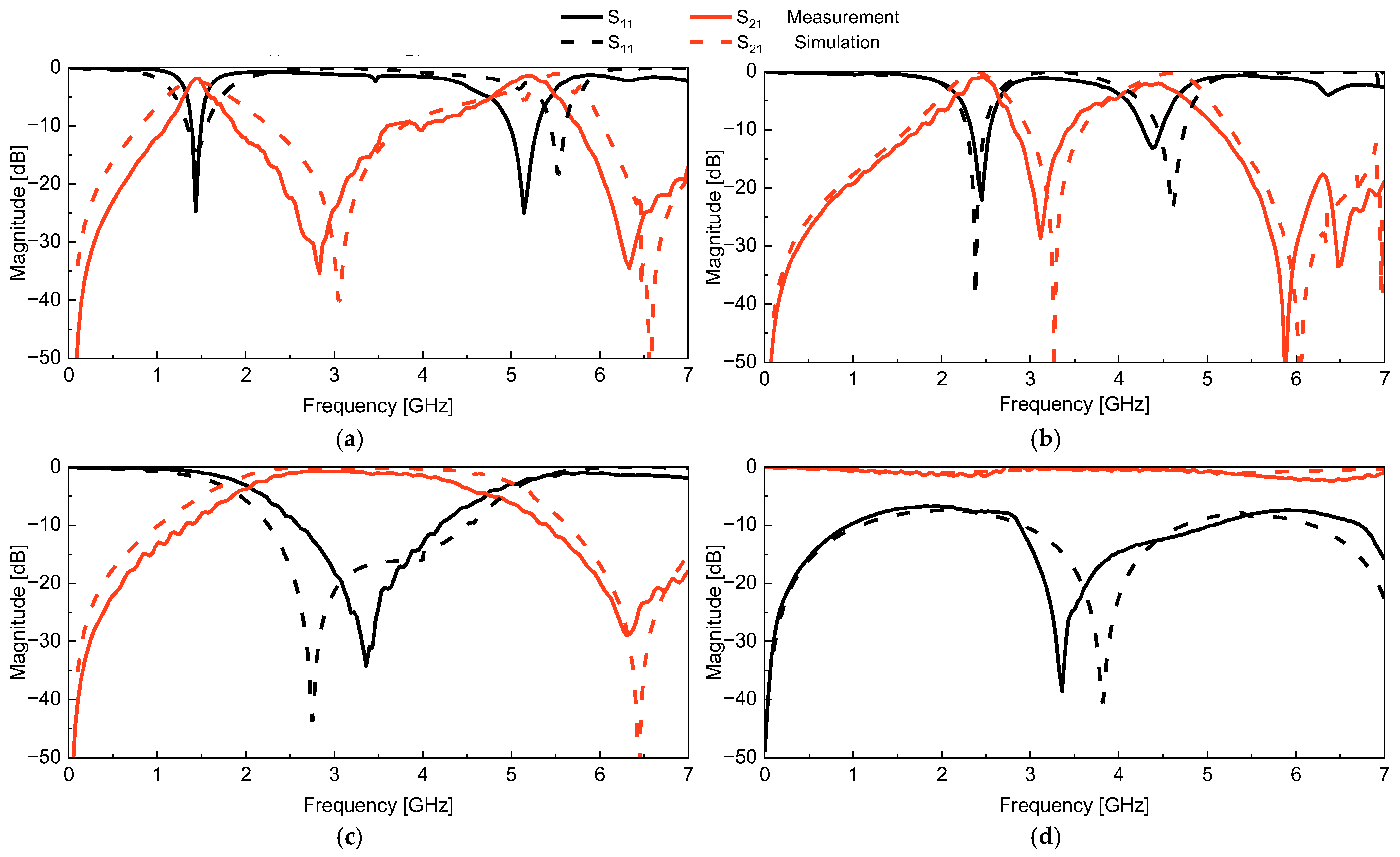

Table 1.
Comparison with previous switchable filters.
| Ref. | Function | BW[%] | IL [dB] | Number of Diodes | Circuit Size [λg×λg] |
| [3] | BSF/ASF/BPF/DBSF | 50.2 / - / 9.7 / 22.1&20 | 1.99 | 4 | 0.21×0.22 |
| [4] | BPF/BSF/DBSF | 53.1 / 30.2 / 3.8 & 2.7 | 0.9 / 2 / 2.2 | 6 | 0.44×0.29 |
| [5] | WBPF / BPF / BSF | 95.7 / 25.3 / 106 | 0.94 / 0.8 | 6 | 0.5×0.25 |
| [6] | BPF/DBPF/BSF | 84.5 / 39.7 & 24.9 / 29.6 | 0.9 / 1.13 & 1.5 / 2 | 6 | 0.61×0.27 |
| [7] | DBPF/DBSF | 25.6 & 20.4 / 30 & 23.1 | 4.6 / 5.6 | 7 | 0.75×0.4 |
| [8] | BPF/BSF | 36.75 / 13 | 1.73 / 0.8 | 7 | 0.74×0.6 |
| [10] | BBPF/DBPF/TBPF | 36.7 / 20.7 & 16.1 /20 & 27.4 & 18.1 | 0.5 / 0.4 / 0.6 | 7 | 0.75×0.4 |
| [11] | BPF/DBPF | 36.07 / 26.42 & 22.92 | 2.9-4.9 | 13 | 0.25×0.25 |
| This work | DBPF/DBPF/WBPF/APF | 23.5 & 14.42 / 23.33 & 13.27 / 73.36 / - | 1.33 & 1.3 / 0.88 & 2.04 / 0.69 / 2.34 | 5 | 0.4×0.05 |
Table 2.
Applied bias voltage conditions and operating modes.
| Condition [V] | Diode State | OperatingMode | ||||||
| V1 | V2 | V3 | V4 | V5 | D1 | D2 | D3 | |
| 4 | 1 | 0 | 0 | 1 | On | Off | Off | Wideband |
| 1 | 3 | 6 | 0 | 1 | Off | On | Off | Dual-band |
| 2 | 4 | 0 | 0 | 1 | Off | Off | Off | Dual-band |
| - | - | - | 1 | 0 | - | - | On | All pass |
- : Don’t care.
Disclaimer/Publisher’s Note: The statements, opinions and data contained in all publications are solely those of the individual author(s) and contributor(s) and not of MDPI and/or the editor(s). MDPI and/or the editor(s) disclaim responsibility for any injury to people or property resulting from any ideas, methods, instructions or products referred to in the content. |
© 2025 by the authors. Licensee MDPI, Basel, Switzerland. This article is an open access article distributed under the terms and conditions of the Creative Commons Attribution (CC BY) license (http://creativecommons.org/licenses/by/4.0/).
Copyright: This open access article is published under a Creative Commons CC BY 4.0 license, which permit the free download, distribution, and reuse, provided that the author and preprint are cited in any reuse.


