Submitted:
24 April 2025
Posted:
28 April 2025
Read the latest preprint version here
Abstract
This review paper presents the recent research work about the design of High-Power and High-Speed (HPHS) Ge-on-Si photodiodes, using Silicon Photonics (SiPh) technology, that are suitable for Radio-over-Fiber scheme 5G technology. In the beginning, the PD principle and structure, such that high RF photogenerated power and wide bandwidth are achieved, are presented. After that, the PD equivalent circuit models are introduced such that it is allowed to obtain the PD S-parameters and bandwidth. Then, the PD theoretical transit-time and RC-time bandwidths are presented, and the PD photocurrent behavior against input optical power and the optical signal manipulation techniques to improve the PD performance are also presented. After that, the impedance matching techniques between the PD output impedance and antenna input impedance are presented. Finally, the recent photonic mmWave antenna designs are introduced.
Keywords:
Ge-on-Si photodiode
; High-Power and High-Speed Photodiode
; Silicon Photonics
; C-band optical signal
; radio-over-fiber
; wireless 5G communication
; mmWave antenna
1. Introduction
The global mobile traffic and the number of subscribers to the wireless network is increasing dramatically with time [1]. Therefore, the 5G network is the key solution for the wireless network to be capable of providing reliable connections for the incoming huge numbers of subscribers and applications. The communication data rates are increasing sharply [1], and the slow electrical components in communications systems will be replaced with fast optical counterparts such that the data rates are allowed to be sharply increased. Furthermore, communications systems are going to be developed into new schemes where electric Radio-Frequency (RF) components are directly interfaced with optical components. As shown in Figure 1, the conversion from the optical to electric domain is achieved using High-Power and High-Speed (HPHS) photodiodes, on the other hand, the conversion from the electric to optical domain is obtained by modulating optical sources. Furthermore, these photodiodes and optical modulators are going to be connected to microwave components such as antennas or electric amplifiers [2]. The photodiodes which are used for wireless communication applications are required to operate with high speeds for higher communications data rates, and high RF photogenerated powers for enhanced Signal-to-Noise Ratios (SNR) and signal coverage range.
The HPHS photodiodes can be designed using the III-V semiconductor material, or they can be achieved using the Silicon Photonics (SiPh) technology. The III-V photodiodes have been reported to achieve high output RF powers with very wide operating bandwidths. However, the III-V photodiodes are very complex to be integrated with the Complementary Metal-Oxide Semiconductor (CMOS) technology making them complex to be integrated with electronics. On the other hand, the Germanium-on-Silicon (Ge-on-Si) photodiodes implemented using the SiPh technology can easily be integrated with the CMOS technology. However, the reported Ge-on-Si photodiodes did not achieve as high powers as the RF powers achieved by III-V photodiodes, and they also did not achieve as wide bandwidths as the bandwidths achieved by III-V photodiodes.
In addition, microwave photonics circuits are much easier to be fabricated using the SiPh platform. On the other hand, if the photodiode is to be designed using the III-V semiconductor material, then it is a complex and high-cost task to fabricate it. In addition, it will also lead into a difficult process to integrate it with SiPh or CMOS systems. The Silicon Photonics technology applies the CMOS processing techniques to obtain photonic, opto-electronic and microwave photonics circuits [3]. On a SiPh chip, many different optical and electrical components can be installed and interfaced, such as Light-Emitting-Diodes, optical waveguides, optical signal processing components, photodiodes, optical modulators, antennas, mmWave circuits and so on [3]. Therefore, the SiPh platform provides a very important opportunity for the optical and microwave components to be integrated together on the same substrate, which will improve the data rates for the 5G technology and beyond.
This review article presents the recent developments in the field of High-Power and High-Speed photodiodes which are used for Radio-over-Fiber (RoF) wireless 5G technology. This article is arranged as follows, Section 2 presents a recent review study for HPHS photodiodes, Section 3 presents important applications for microwave photonics circuits using HPHS photodiodes, and Section 4 concludes the paper.
2. High-Power and High-Speed RF Photodiodes
It has been reported that the photodiodes designed using the III-V semiconductor material on an Indium Phosphide (InP) substrate can provide high output RF powers which can sufficiently cover required wireless ranges for 5G base-stations radiations at mmwave frequencies [4]. The RF photogenerated power of III-V photodiodes reaches 25 dBm at 25 GHz, and 15 dBm at 65 GHz [4]. However, the III-V photodiodes are complex and high-cost to be fabricated, and they are difficult to be integrated with CMOS and SiPh technology. On the other hand, the Ge-on-Si photodiodes, designed using SiPh technology, could provide sufficient output RF photogenerated powers at mmwave frequencies. Many High-Power and High-Speed (HPHS) Ge-on-Si photodiodes have been recently reported to be implemented for microwave photonics applications [5,6,7,8,9,10,11,12,13,14,15,16,17,18,19,20,21,22,23,24,25,26]. HPHS Ge-on-Si photodiodes can be achieved when the Ge absorbing region is optically fed using evanescent coupling with double lateral Silicon Nitride waveguides [5]. They can also be obtained using a mode-evolution-based coupler which illuminates the light into the Ge region uniformly to reduce the saturation effects at high input optical powers [6,7]. In addition, they can be achieved when many photodiodes are connected in parallel to form a photodiode linear array [8,9,10,11,12,13,14]. Also, when the doping concentrations for the photodiodes are regulated such that the space-charge screening effect is sharply decreased [15]. In addition, HPHS photodiodes (PDs) can be achieved when it is constructed using stacking N-, intrinsic- and P-type doped regions, and the light is evanescently coupled into the Ge region [16,17]. Furthermore, HPHS PDs can be achieved using the Uni-Traveling Carrier (UTC) approach, where the electrons are the only allowed carriers and the slow holes are blocked and excluded [18]. UTC PDs can also be achieved using the III-V material and then they are integrated heterogeneously on the Silicon (Si) substrate [19]. The avalanche gain can also be utilized to provide HPHS Ge-on-Si PDs [20,21,22,23], however, most of the Avalanche PDs are designed for data communications applications at the O-band. Traveling-wave photodiodes can also be employed to achieve HPHS PDs [24,25]. It was also found that when the optical field is manipulated properly around the Ge absorbing region, then higher output RF powers are expected to be obtained from the PDs [26]. Table 1 presents the performance comparison between the introduced Ge-on-Si PDs.
It is worth mentioning that Germanium is a good medium for absorbing optical signals with wavelengths just before 1600 nm [27]. The absorption coefficients of Ge medium are at , and at . Therefore, the Ge material is a very good option to be used as the absorbing medium for photodiodes which are used for data centers at 1300 nm, and it is also a good option for the photodiodes which can be used for 5G base-stations at 1550 nm. However, InGaAs material is more efficient at 1550 nm wavelength, however Ge is used for PD design as it is much easier to be integrated within a Silicon chip using the SiPh platform.
2.1. Photodiode Principle and Structures
When the light is evanescently coupled from double lateral waveguides to the Ge region, the PD is expected to provide high-power and high-speed operation [5]. The evanescently coupled PD is shown in Figure 2. The light distribution in the absorption Ge region is uniform due to the tapering of the lateral waveguides. As a result, the photogenerated carriers are not concentrated at a specific location, and the operating bandwidth of the PD is increased. In addition, the applied electrostatic field between the PD electrodes is sufficiently strong due to the used doping concentrations for the N+-, P- and P+-region. Therefore, the collection of the photogenerated carriers is fast and efficient. The lateral waveguides are sufficiently long such that the injected photons are fully absorbed as they travel along the Ge region. Phase matching between the waveguide modes and the Ge region modes should be achieved such that efficient light coupling is obtained [28]. Many parameters affect the mode coupling condition such as the waveguide thickness, the Ge region thickness, the refractive indices of the waveguide and Ge region, and the operating wavelength.
When the photodiode is operated under high-power conditions, that is when the input optical power is 10 mW or more, then the photodiode suffers from degraded linearity, heat failure occurrence, losing the mode matching between the waveguide and Ge region, and accumulation of charges causing the space-charge effects to take place. The mode-evolution-coupling technique can be used to achieve HPHS PDs [6,7]. Figure 3 shows the proposed mode-evolution-based coupled HPHS PD in [7]. The optical light is divided into two optical waveguides using a Multimode Interferometer (MMI) power divider such that two parallel Ge regions are equally fed using the mode-evolution-based coupling technique. The mode-evolution-based coupler is composed of the waveguide bend and the linearly tapered waveguides. The waveguide bend reduces the mode mismatch between the waveguide and Ge region, therefore, the bend radius should be as large as possible to achieve a gradual mode transition. The waveguide taper allows the light to couple into the Ge region gradually and efficiently, as a result, uniformly distributed optical generation rate along the PD length is achieved, and the PD saturation current is improved. The waveguide taper length should be as long as possible to increase the PD responsivity, however, the PD bandwidth will be reduced due to the capacitance increase. It is worth noting that when the Ge region was divided into two halves, the input optical power at each Ge region is reduced by half, the space-charge effects are much reduced and the saturation current is much improved. The proposed HPHS PD in [7] achieved a dark current of 73 nA at reverse bias, and a photocurrent of 9.4 mA at an input optical power of 20 mW. The high-power operating bandwidth of the PD is 31.6 GHz when the input optical power is 4 mW.
Furthermore, the Ge regions can be connected in parallel using a single Ground-Signal-Ground (GSG) terminal to enhance the output power of the photodiode [8,9,10,11,12,13,14]. When two Ge regions are connected in parallel, then the total Ge area is increased by two times. As a result, the junction capacitance increases by a factor of two, and the series resistance decreases by a factor of two also, as a result, the PD RC-time bandwidth is not changed and the PD saturation current is sharply increased. Hence, the PD output RF power is increased sharply as well. The array of two elements proposed in [8] is illuminated by light from the front and back sides of the Ge regions, as a result, the absorption rate along the Ge regions has a uniform distribution causing the space-charge effects to be reduced sharply, and at the same time, the saturation current increases sharply. In addition, when the PD is illuminated by light from both sides, then the applied optical power on the Ge regions is reduced by a factor of 0.5, which decreases the chances of thermal failures sharply. The dark current of the PD array has increased, compared to the dark current of the single-element PD.
When the number of elements of the PD array is increased to be more than two elements, then the PD array saturation current will be increased, but the PD array RC bandwidth will be changed from that of the single-element PD because the PDs resistances will not be connected in parallel. Therefore, the RC bandwidth of the PD array can be calculated using the transmission matrix method for the analysis of the resulted complicated PD equivalent circuit, as was proposed in [9] where all the Ge regions share the same P+ doped region. It was found that when more than two array elements are used, then the PD array bandwidth will be reduced as the junction capacitance increase will be the dominant affecting factor, and the array total resistance will not decrease. However, the bandwidth of the PD array can be enhanced using inductive peaking techniques and transmission line theory. The saturation current of the PD array with more than two array elements will increase gradually, because there will be high power losses in the P+ doped region resistances, and due to out-of-phase currents flowing in these resistances [9].
Traveling Wave PD Array (TWPDA) can also be designed in order to avoid the bandwidth reduction due to using more than two array elements [10]. The used single-element PD for the four-element TWPDA proposed in [10] is a PIN PD [16,28,29] with a high photocurrent and a wide bandwidth. The impedance matching between the TWPDA and a 50 Ohm load is achieved by optimizing the GSG coplanar-waveguide electrodes which are connected to the four PD elements, taking the periodic capacitive PD loading into consideration. In addition, it can be seen from Figure 4, showing the proposed TWPDA in [10], that optical delay lines are used in order to match the optical velocity with the electrical velocity. On the other hand, it can be seen from Figure 5, showing the proposed TWPDA in [11], that this proposed PD array has single-element PDs illuminated from front and back sides such that the power handling capability of the PD array is doubled.
The traveling wave photodiode approach was also used to provide a High-power and High-Speed Photodiode as proposed in [24,25]. The traveling wave photodiodes are designed with metallic electrodes that achieve the impedance matching with an external circuit. The transmission line theory is used to provide the impedance matching between the microstrip or coplanar waveguide electrode lines and the output circuit (50 Ohm load for example). The input terminal of the electrodes will also be connected to a matched load such the backward traveling waves are absorbed and not reflected back to the transmission lines. Hence, the TWPD bandwidth is engineered using the transmission line theory, and it will also be impacted by the PD RC-time bandwidth, carrier drift time, carrier diffusion, carrier trapping, and the bandwidth of velocity matching between the electrical and optical signal. It can be seen from Figure 6 that the proposed TWPD in [25] is optically dual-injected and evanescently coupled to the Ge region. The TWPD length is optimized such that the best PD performance is achieved when the uniform light distribution takes place in the Ge region because the left- and right-incoming optical signals will add up constructively to provide a uniform distribution. As a result, the effective absorption area is increased, and the saturation performance is much improved. The 3 dB bandwidth of this proposed TWPD is limited by the RC time constant, the carrier transit time, and the electrodes length. When the PD electrodes are longer, the PD capacitance and transmission line loss is increased, as a result, the PD bandwidth decreases. Also, when the PD length provides non-uniform light field distribution, then the bandwidth will decrease because of increased space-charge screening effects. Also, the PD bandwidth will be decreased when the input optical power is increased due to the increase in the space-charge screening effects and the much higher probabilities of carriers collisions with the lattice.
The HPHS PD can also be achieved when doping concentrations are regulated such that the space-charge screening effects are significantly reduced [15]. The doping-regulated Ge-on-Si PD is shown in Figure 7 where it can be seen that the Ge region is sandwiched between N++ doped region and P+ and P++ doped regions. When the doping concentration in the P+ collection layer is increased such that the number of holes in the collection layer is much more than the photogenerated carriers in the absorption Ge region, then the built-in electric field is much enhanced. As a result, the carriers transport speed is much enhanced such that it achieves saturation velocity, the carriers transit time is much reduced, the probability of carriers recombination is reduced, the photocurrent and saturation current are much increased, and the space-charge screening effects are eliminated.
In addition, when the optical signal is coupled evanescently to the Ge region of the PIN PD, then high-power at high speeds PDs can be achieved as they were reported in [16,17]. Also, Uni-Traveling Carrier (UTC) PD, where the only allowed carriers are the electrons, can be designed using Ge-on-Si approach or using the heterogeneously integrated III-V material on Silicon (Si) to achieve HPHS PD performance [18,19].
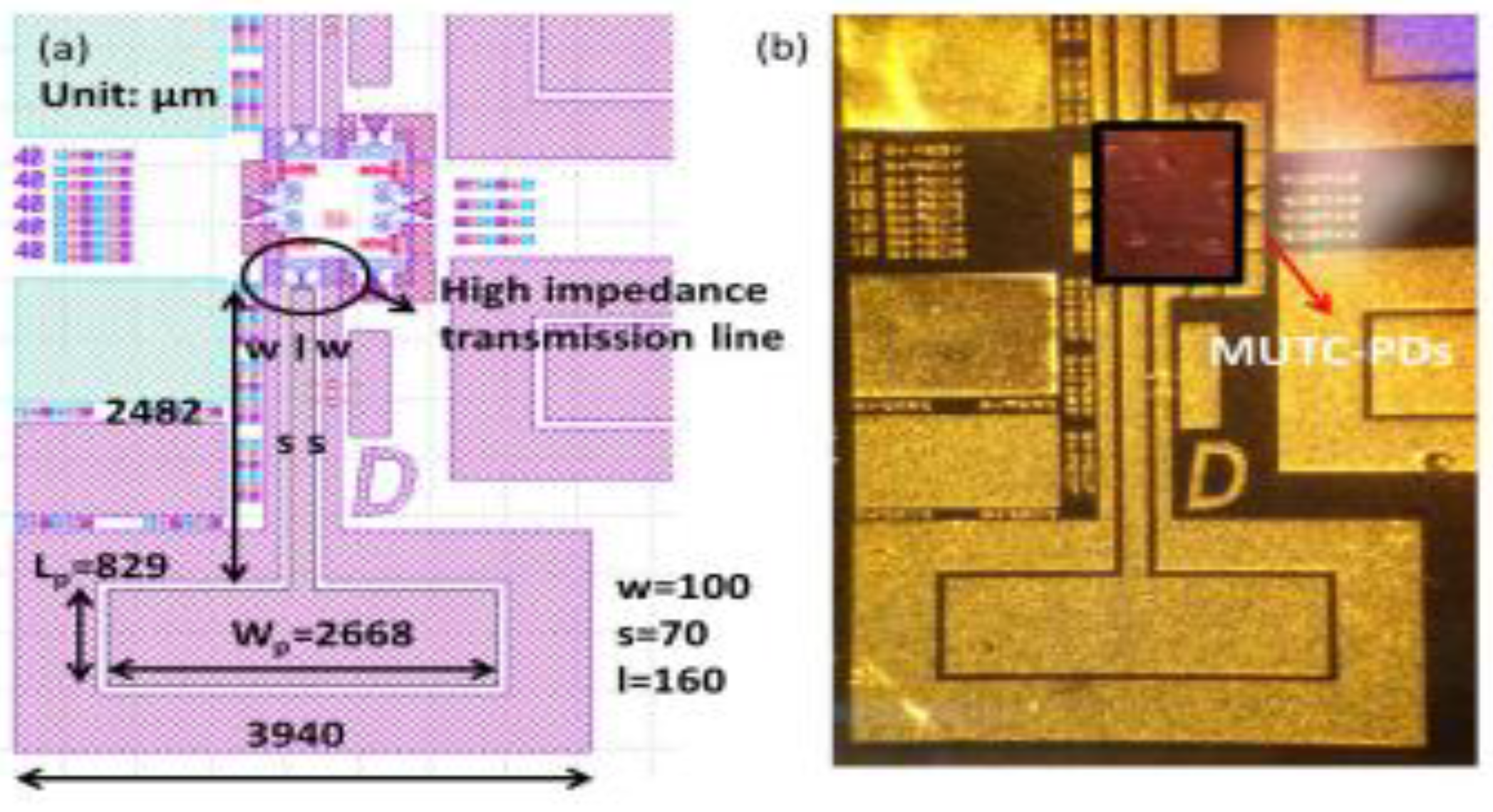
Finally, the avalanche gain can be utilized to increase the Ge-on-Si PD output power as proposed in [20,21,22,23]. However, these Avalanche Ge-on-Si PDs are reported to be used for data communications within data centers, and not for 5G base-stations with the ROF scheme. Hence, they are briefly presented here to show that using the Avalanche gain could introduce the opportunity of achieving HPHS PDs for 5G Base-station applications. The proposed Avalanche PhotoDiode (APD) is presented in Figure 8 showing an example of an APD design. This proposed APD design achieves a bandwidth of 18.9 GHz, DC photocurrent gain of 15, and a sensitivity of – 11.4 dBm at a reverse bias of – 6 V. It can be seen from Figure 8 that the APD has three terminals, and the Ge region is installed on top of the Si waveguide, and the waveguide is installed on top of a Si substrate. The optical signal is evanescently coupled to the Ge region for absorption. The top side of the Ge region is P-doped and connected to terminal one, while the Si substrate is composed of interdigitated N- and P-doped fingers which are spaced using intrinsic silicon. The P-doped fingers are connected to terminal two, and the N-doped fingers are connected to the third terminal. As a result, two reversed-biased PIN diodes are achieved, and the light absorption region is independently controlled from the charge multiplication region.

Table 1.
Comparison table between the introduced HPHS Ge-on-Si photodiodes in this article.
| Photodiode | Responsivity (A/W) | Photocurrent for High-Frequency (mA) | Electric Bandwidth (GHz) | RF power (dBm) | Dark current (uA) | Application | DC photocurrent |
| Evanescent-Coupled PD [5] | 0.52 | 12 mA | 36 GHz | 8.57 dBm | 0.1 | High-power | 16 mA |
| Mode-Evolution PD [7] | 0.47 | 1.88 mA | 31.6 GHz | -7.53 dBm | 0.073 | High power | 9 mA |
| 2-Element Array PD [8] | 0.46 | 13 mA | 9 GHz | 9.27 dBm | 1.28 | High Power | 28.8 mA |
| 8-Element Array PD [9] | 0.77 | 1 mA | 4.1 GHz | -13.01 dBm | 3.46 | High Power | 37 mA |
| Travelling-Wave PD 4-Element Array [10] | 0.82 | 20 GHz | High Power | 65 mA | |||
| 4-Element TWPDA [11] | 0.76 | 13 mA | 35 GHz | 9.26 dBm | >3.5 | High Power | 112 mA |
| Traveling Wave PD [25] | 1.07 | 11.4 GHz | 0.0099 | High Power | 13.28 mA | ||
| 8-Element PD Array [12] | 0.21 | 48 mA | 5 GHz | 14.3 dBm | 15 | High Power | |
| 4-Element PD Array [14] | 0.58 | 19 mA | 15 GHz | 7 dBm | 0.3 | High Power | |
| Doping Regulated PD [15] | 1.06 | 5.3 mA | 20 GHz | 1.5 dBm | 0.0014 | High Power | 36.4 mA |
| PIN PD [16] | 40 mA | 4.38 GHz | 14.17 dBm | 125 | High Power | ||
| Si-Based UTC PD [18] | 0.5 | 2 mA | 30 GHz | -11.7 dBm | 20 | High power | |
| III-V UTC PD on Si [19] | 0.95 | 40 GHz | 12 dBm | 0.01 | High Power | ||
| Avalanche PD [20] | 0.65 | 27 GHz | low | 100 | Low-Power Data Commuications | ||
| Avalanche PD [21] | 14 GHz | low | Low-Power Data Commuications | ||||
| Avalanche PD [23] | 18.9 | low | Low-Power Data Commuications |
2.2. Photodiode Equivalent Circuit Models
A fundamental equivalent circuit for a photodiode can be presented as shown in Figure 9 [5], where Cj represents the PD junction capacitance in the Ge absorption region, Cp represents the parasitic capacitance between the conductors of the Coplanar Waveguide (CPW) line, and Rs represents the series resistance of the highly P- and N-doped regions at the ohmic contacts on Silicon and Germanium. The junction capacitance is a function of bias voltage and the Ge region geometry. While the series resistance is a function of the doping concentrations at the ohmic contacts, and its value is usually around when the PD area is small. It can be clearly seen from Figure 9 that this PD equivalent circuit reveals the RC-time performance of the Ge-on-Si photodiode. In addition, many parameters were ignored in this equivalent circuit as their effects on the PD performance are negligible. A more detailed equivalent circuit is presented on Figure 10 [18], where the CPW conductors are represented using the series inductance Lpad, and the shunt capacitance Cpad. In addition, the junction resistance Rp is also included. This resistance is usually very high because of the very small dark current, and it is usually safe to ignore this junction resistance.
A more involved RF small-signal equivalent PD circuit is presented on Figure 11 [30], where the transit time and the RC time effects are included. It can be seen that the input Radio-Frequency optical power component is represented by the input voltage source , followed by the PD transit-time equivalent circuit including and , where their values are optimized in the beginning such that the PD transit-time bandwidth is correctly achieved. The transit-time bandwidth is usually very high with values that could reach to around or more, therefore it can be ignored when the targeted operating frequencies are well below 100 GHz. The output voltage represents the generated RF electric field in the PD absorption region, this generated electric field drifts the free carriers to the PD external circuit. Therefore, the PD photocurrent is represented by the voltage-dependent current source , which is dependent on the generated RF electric field in the PD absorption region and the PD responsivity . The PD photocurrent feeds the RC-time equivalent circuit and the PD load. The PD equivalent circuit in Figure 11 provides a more accurate frequency response for the photodiode. It is worth to highlight that the output RF power from the photodiode is limited by the space-charge screening effects and thermal failure. When the photodiode is operated under low-power conditions, the photodiode operates in its linear region since the electric field in the depletion region is not collapsed and free carriers drift with constant saturation velocity, as a result the PD equivalent circuit is independent of the input optical power. On the other hand, the equivalent circuit will be dependent on the input optical power when the photodiode is operated under high-power conditions, because the PD transit-time and junction capacitance become dependent functions of the input optical power, as a result, the output RF power varies nonlinearly with the input optical power.
It can be seen from Figure 12 and Figure 13 [31,32] that the PD equivalent circuit can also be designed including the CPW line model, where the S-parameters of the CPW line are included in the CPW line model in the equivalent circuit. It can be seen from Figure 13 that the PD CPW line is designed with an inductive-peaking transmission line tapered to a line. Therefore, inductive peaking is achieved to enhance the photodiode bandwidth.
The equivalent circuit of the photodiode array when it is composed of two elements is presented on Figure 14 and Figure 15(b), [7,8]. It can be seen from Figure 14 and Figure 15(b) that the PD bandwidth is not decreased when two array elements are used, because the two Ge regions are connected in parallel, and while the total junction capacitance is doubled, the total photodiode resistance is halved at the same time. As a result, the bandwidth of the PD array with two elements will not be decreased when compared with the corresponding single-element PD bandwidth. This fact can be obvious to obtain from Figure 15(b), where it can be seen that the junction capacitances of the two Ge regions and the element resistances are connected in parallel. This shunt topology in Figure 15(b) is chosen because the two Ge regions are connected in parallel as it is presented in Figure 14. It can be seen from Figure 14 that the PD element junction is available in the Ge region, and the top N++ Ge regions of the two elements are connected to the same ground electrode, while the P++ Si region of the two elements are connected to the same signal electrode. As a result, the two Ge regions are actually connected in parallel.
On the other hand, when the PD array is composed of more than two elements connected in parallel as shown in Figure 16 [9], then the bandwidth of the PD array will be decreased. This is because the elements’ resistances and junction capacitances, and in Figure 16, are not connected in parallel, and this equivalent circuit should be analyzed using different mathematical approaches to find the PD array bandwidth; e.g., the transmission matrix method can be used to find the frequency response of the PD array with more than two elements. The power loss in the PD array with more than two elements will also increase, however, the overall saturation photocurrent will increase sharply as the number of elements increases.
2.3. Photodiode Bandwidth Design
The electrical 3 dB bandwidth of the photodiode is dominantly limited by the RC- time and transit-time bandwidths. The RC- and transit-time bandwidths can be obtained from the photodiode equivalent circuit. The carrier transit-time bandwidth for the Ge-on-Si PD in [5] was found to be calculated as shown in Eq. (1).
where is the carrier drift velocity, and is the thickness of the Ge region. The carrier drift velocity depends on the electric field strength; it is for the Ge medium [5]. The carrier transit-time can be defined as the required time for the photogenerated electrons and holes to travel from the absorption region to the collecting electrical electrodes. The transit-time bandwidth for Ge-on-Si photodiodes is dominantly limited by the holes drift velocity because the holes are slower than electrons. On the other hand, the RC-time bandwidth was found to be calculated as shown in Eq. (2), [5,7].
where is the total PD resistance including the PD series ohmic-contact resistance, junction resistance, and load resistance, and is the total PD capacitance including the junction and parasitic capacitances. If the load resistance is set to zero, then the resistance can be found as shown in Eq. (3) [5].
where is the PD junction resistance, and is the series contact resistance. The junction capacitance can be found as shown in Eq. (4).
where is the dielectric constant of the Ge medium, is the PD active area, and is the depletion region depth.
The overall electrical 3 dB bandwidth can be found as shown in Eq. (5) [5].
The electrical 3 dB low-pass bandwidth of the photodiode will be dominantly determined by the RC-time bandwidth if the Ge thickness is small, and the frequency of operation is not too high. It is worth highlighting the trade-off that occurs between the transit- and RC-time bandwidths. When the Ge thickness is decreased to improve the transit-time bandwidth, the RC-time bandwidth will be degraded, and vice versa. In addition, the photodiode bandwidth, saturation RF power and PD linearity are dependent parameters on the bias voltage and input optical power. When the bias voltage changes, the junction capacitance varies because the PD depletion region width was varied, as a result, the RC-time bandwidth is varied. On the other hand, when the input optical power increases, the space-charge screening effects increases and the electric field in the absorption region decreases, as a result, the carrier velocity decreases and the transit-time bandwidth decreases.
The RC bandwidth of the PD array of two elements is equal to the RC bandwidth of the single-element PD. This part proves this concept mathematically. The RC-time bandwidth of the single-element PD can be written as shown in Eq. (6) [8].
And the RC-time bandwidth of two-element PD array is shown in Eq. (7) [8].
It can be seen from Eq. (6) and Eq. (7) that total resistance of the PD array is divided by 2, and its total capacitance is multiplied by 2, because the two Ge regions are connected in parallel. Therefore, it can be seen from Eq. (6) and Eq. (7) that the RC bandwidth of the two-element PD array is almost equal to the RC bandwidth of the single-element PD. However, when the number of array elements is more than two elements, then PD array bandwidth decreases as the number of elements increases.
2.4. Photodiode Saturation Current and RF Power
The photocurrent versus optical power characteristics of this proposed PD in [25] show that three photodiode operation regions can be deduced as shown on Figure 17. The first operation region is obtained where the photocurrent is linearly increased versus the input optical power, because the Ge region is not saturated yet. The second operation region is obtained where the photocurrent increases also linearly with the input optical power but with a different slope, because the Ge region in this operation region is partially saturated, and the saturated PD volume increases with the input optical power increase. The third operation region is the saturation region where the carriers in the Ge region are fully saturated; the carriers inside the light field distribution are fully saturated, and as a result, the photocurrent does not increase when the optical power increases.
In general, the output RF photogenerated power can be found in using Eq. (8). In addition, the saturation current which starts in the nonlinear operation region can be defined as the average photocurrent at which the RF power compressions curve drops by from its peak value.
It is worth noting that the PD power handling capability and saturation performance can be much improved when the incident light field is illuminated on the double sides of the Ge absorption region using different optimized manipulation approaches which will allow the absorption profile to spread more uniformly across the PD absorption region. Different light manipulation approaches are proposed in [26] as shown in Figure 18. Type B PD has three sections, where section 1 is used to generate multi-modes and the light is manipulated to provide a good pattern before reaching the Ge region, section 2 allows the light to be illuminated in the front and side parts and results in an optimized light distribution and a new absorption profile in the Ge region, and section 3 is designed such that the light is fully absorbed. Type B PD is modified to be double-sided illuminated using a MMI (MultiMode Interferometer) splitter which is shown as type C PD in Figure 18. It was found that the dark current for the three types are almost the same. The saturation current increases sharply when going from type A to type C, and the PD bandwidth increases sharply under high-power operations. The low-power operations bandwidth does not vary a lot when going from type A to type C PD.
3. Photodiode Integrated Photonic Applications
3.1. MMWave Matching Network Design
The photodiode is a capacitive source, and an inductive matching network is required to be designed between a photodiode and microwave load. The matching network can be designed directly on the photodiode substrate, or on a separate substrate where wire bonding or flip-chip bonding are used to connect the matching network to the photodiode. A microwave load is designed with an input impedance of , however, this microwave load impedance is low such that it degrades the photodiode sensitivity because of high thermal noise and weaker absorption for the RF photogenerated power. The photodiode matching network is designed to achieve complex conjugate matching between a photodiode and microwave load using three approaches. First, a matching network is designed between the photodiode and a microwave load. This matching network is designed using spiral inductors, quarter-wavelength transformers, matching open- or short-circuited shunt CPW stubs, and inductive peaking transmission lines. The inductive peaking transmission line is designed to have a very high characteristic impedance tapered to a low characteristic impedance line to be matched with the microwave load input impedance. The inductive peaking transmission lines are also used to improve the photodiode bandwidth. Second, the antenna input impedance is engineered such that it achieves an inductive reactance that is slowly-varying with respect to frequency. The third approach is achieved when a trans-impedance amplifier is used to achieve the impedance matching between a photodiode and microwave load.
The first approach is shown to be used as in Figure 19 where resonating mmWave matching networks are presented [36,37]. These resonating matching networks provided a narrow matching bandwidth. It can be seen from Figure 19 that these matching networks are composed of CPW quarter-wavelength transformers and inductive peaking lines. It can also be seen that DC block capacitors are used such that the RF signal is blocked from flowing to the DC bias network, and forced to flow into the microwave load.
The second matching approach can be seen in Figure 20 and Figure 21, where the antenna input impedance is achieved to be inductive and compensating for the capacitive reactance of a photodiode [38,39]. The antenna geometrical parameters are optimized to achieve the complex conjugate matching between the photodiode and antenna. The Connected-Array antenna of bowtie elements are designed on Aluminum Nitride (AlN) substrate [38]. The substrate thickness and dielectric constant of the AlN substrate were optimized to control the antenna input real-part impedance, while the input inductive reactive impedance was achieved using the inductive peaking technique using a coplanar strip line and wire bonds. Furthermore, the antenna metallic dimensions can be optimized to achieve the complex conjugate matching as shown for the proposed Short Asymmetric Inductive Dipole (SAID) antenna in [39]. The proposed photonic antenna in [39] achieved a reconfigurable bandwidth in the frequency range from 26.5 to 40 GHz. The antenna input real-part impedance was controlled using the ground and dipole dimensions, and the proximity spacing between the dipole and ground. On the other hand, the antenna input inductive imaginary-part impedance was achieved using the two metallic loops around the feeding CPW pads.
The third impedance-matching approach is achieved using a trans-impedance amplifier [40] as shown in Figure 22. It can be seen from Figure 22 that three transistors are used to step up the photodiode low output impedance to . Unfortunately, this trans-impedance amplifier consumes a lot of power, and achieved a narrow matching bandwidth.
Furthermore, the photonic matching network should also incorporate a bias-tee such that the photodiode is properly DC reverse biased, and the RF signal is blocked from flowing to the DC biasing network [41,42]. The DC bias is blocked from flowing into the RF load using an interdigital capacitor as shown in Figure 23 and Figure 24. On the other hand, the RF signal is isolated from flowing into the DC biasing network using a grounded CPW open-circuited shunt stub as shown in Figure 23, or using a band-reject filter as shown in Figure 24. The proposed bias-tee in [41] was designed to operate in the frequency band from to while the bias-tee in [42] operates from to
3.2. Photodiode Integrated Photonic Emitters
A photonic-integrated quarter-wavelength monopole antenna was designed at 15 GHz on a Silicon chip with a volume of , a gain of , and a bandwidth of [43]. The proposed design is shown in Figure 25. The photodiode is connected at the GSG pads shown in Figure 25, where the photodiode is a Ge-on-Si photodiode designed to be operated under low-power conditions.
The proposed photonic antenna in [45] was designed in the bandwidth with two matching approaches. The first approach is when the photodiode has its own matching network to , and the antenna is designed to be well matched to , and then the photodiode with its matching network is connected to the antenna. while the second approach was to use the antenna input impedance to achieve the complex conjugate matching with the photodiode output impedance. The proposed photonic antenna in [45] is shown in Figure 26. The output RF current from the photodiode is fed to a patch antenna using a probe feed that goes through an air-filled cavity. The bottom face of the air-filled cavity include a slot element that divides the cavity into two coupled half-mode cavities, and excites the patch antenna. Therefore, two modes are excited to widen the operating bandwidth.
The proposed photonic antenna design in [48] achieved the complex conjugate impedance matching using the antenna geometry optimization. The proposed photonic antenna in [48] is shown in Figure 27. The antenna is a short asymmetrical inductive dipole achieving a low cross-polarization level, high radiation efficiency, a bandwidth from to , and a frequency reconfigurability feature when the photodiode reverse bias voltage is varied. It can be seen that two parallel folded dipoles are used to achieve an impedance transformation and a slowly-varying input impedance with respect to frequency. The antenna theory of operation was explained using the Transmission-Line Mode (TLM) and Radiating Mode (RM). As a result, the characteristic impedance of the Transmission-Line Mode stub and the radius of an equivalent dipole for the proposed antenna can be obtained. Therefore, the antenna input impedance is found considering that the antenna is composed of two parallel monopoles with a lower truncated arm. It was found that the antenna input impedance incorporates a step-up impedance ratio, the impedance of the parallel monopoles, and the coplanar short-circuited stub impedance. Therefore, the real-part of the antenna input impedance was contributed using the TLM and the imaginary part is contributed using the RM.
The work in [46] had also integrated a mmWave antenna at 100 GHz with two UTC photodiodes as shown in Figure 28. The RF signal is fed into the radiating antenna aperture using a coupling slot such that the DC signal is blocked from flowing to the radiating antenna. It can be seen from Figure 28(b) that the antenna radiating aperture is made of symmetrical modulated metasurface arrays which are fed using out of phase RF fields. The metasurface array is made of a capacitive impedance boundary condition which is sinusoidally modulated along the field propagation direction. The inductive boundary condition is also obtained due to the use of an inductive grounded substrate. Therefore, a transverse-magnetic surface waves will propagate, and radiate because of the periodic modulation.
The photonic-integrated antenna at , as shown in Figure 29, was designed to achieve beam steering [47]. It can be seen that the radiating structure is composed of two stacking patches on a single-mode cavity to achieve a wide operating bandwidth. It can be seen that the RF signal propagates through Substrate Integrated Waveguides (SIWs) to finally couple to the radiating structure. The array grating lobes are reduced due to using eight elements along the antenna H-plane, and two elements along the E-plane. This proposed array is connected to a UTC photodiode, and the beam steering is achieved using optical phase shifters.
The photonic-integrated antenna array in [49] was designed to operate in the frequency range from to using a single-element Leaky-Wave antenna with beam steering occurring with respect to the operating frequency. The proposed photonic Leaky-Wave antenna array is shown in Figure 30, where it can be seen that two UTC photodiodes are used to feed the antenna array. The single-element Leaky-Wave antenna is composed of four periodic unit-cells connected in series to a microstrip line, and a patch element connected at the antenna end. The proposed unit-cell is also presented in Figure 30, it is composed of four half-wavelength open-circuited shunt stubs used to introduce high-impedance points along the microstrip line. Therefore, the propagating electromagnetic waves will be perturbed by these high-impedance points, as a result, signal reflections and losses will take place. The single-element Leaky-Wave antenna is optimized such that the reflections are minimized and the radiations are maximized, and the remaining waves reaching to the antenna end will be radiated using the patch. This proposed Leaky-Wave antenna array achieved a directivity of , and a frequency beam-scanning range of .
The proposed photonic two-element array in [50] used travelling-wave antenna because of its slowly-varying input impedance versus frequency. The proposed array is shown in Figure 31, where it can be seen that it is composed of two array elements. The proposed antenna array provided a gain of in the operating bandwidths from to and from to 86 GHz. It was also found that the radiated power from the array is −6.7 dBm at 70 GHz.
The Bowtie antenna was used to achieve a photonic-integrated antenna at 2.5 THz [51], photonic-integrated Connected Array antenna at 20 GHz [38], and a linear array at 50 GHz [54]. The proposed photonic-integrated Connected Array antenna shown in Figure 32 [38] presented a wideband of operation from 5 to 20 GHz thanks to using the single-element Bowtie antenna. The used four photodiodes are Charge-Compensated Modified UTC photodiodes with an output RF power of 23 dBm at 20 GHz for a single photodiode. Flip-chip bonding was used to connect the photodiode to the used Aluminum Nitride (AlN) substrate to increase the photodiode peak RF power. In addition, the used coplanar strip output and the wirebonds were used to increase the inductive load for the photodiode such that the impedance matching is improved. Tuning the thickness and dielectric constant of the used AlN substrate improved the impedance matching between the antenna and photodiode. It is worth noting that the small gap between adjacent Bowties works as a capacitive RF short between the array columns, therefore, a current sheet is achieved which produce broadside radiation patterns. The proposed photonic Connected Array antenna was capable to steer the beam to and the achieved radiated power from the antenna was more than up to
Also, the coplanar-patch antennas at were connected to a photodiode [52,53]. It was found in [53] that the photonic-integrated coplanar-patch, shown in Figure 33, achieved a gain of thanks to using the inductive peaking matching technique and the used low-loss AlN substrate. While the coplanar-patch antenna, with bandwidth from to , in [52] achieved a gain of because of the used lossy Silicon substrate.
4. Conclusions
This review paper presents the recent research work about the design of High-Power and High-Speed SiPh Ge-on-Si photodiodes for RoF 5G communications applications. It was introduced in this article that the HPHS Ge-on-Si PDs show that they are real candidates for the RoF-scheme 5G technology, because these PDs achieve sufficient RF photogenerated powers at mmWave frequencies. The principle and structure for the HPHS SiPh Ge-on-Si photodiodes are introduced first, then the equivalent circuit model for the Ge-on-Si photodiode, such that it is possible to obtain the PD S-parameters and bandwidth, is presented. After that, the PD transit-time and RC-time bandwidths are presented and the impact of the linear PD array on the overall bandwidth was also discussed. After that, the PD photocurrent behavior against the input optical power is discussed, in addition, the RF photogenerated current mathematics and the optical signal manipulation techniques to improve the saturation current and bandwidth are discussed. Lastly, the matching network design techniques to match the PD with mmWave antennas are introduced, and the recent photonic mmWave antenna design is also presented.
Author Contributions
Conceptualization, S.H.; methodology, software, S.H.; validation, S.H.; formal analysis, S.H.; investigation, S.H.; resources, S.H.; data curation, S.H.; writing—original draft preparation, S.H.; writing—review and editing, S.H., F.F., X.Z., A.K. ; visualization, S.H.; supervision, F.F., X.Z, A.K. ; project administration, F.F., X.Z., A.K.; funding acquisition, F.F., X.Z., A.K. All authors have read and agreed to the published version of the manuscript.
Funding
Please add: This work was supported by Fonds de Recherche du Québec – Nature et Technologie (FRQNT, Québec).
Institutional Review Board Statement
Not applicable.
Informed Consent Statement
Not applicable.
Data Availability Statement
All data are available within the manuscript.
Conflicts of Interest
The authors declare no conflict of interest.
References
- “Cisco annual internet Report - Cisco Annual Internet Report (2018–2023) White Paper,” Cisco. Available online: https://www.cisco.com/c/en/us/solutions/collateral/executive-perspectives/annual-internet-report/white-paper-c11-741490.html (accessed on 18 July 2023).
- T. Nagayama, S. Akiba, T. Tomura, and J. Hirokawa, “Photonics-Based MilliMeter-Wave Band Remote Beamforming of Array-Antenna Integrated with Photodiode Using Variable Optical Delay Line and Attenuator,” Journal of Lightwave Technology, vol. 36, no. 19, pp. 4416–4422, 2018. [CrossRef]
- S. Y. Siew, B. Li, F. Gao, H. Y. Zheng, W. Zhang, P. Guo, S. W. Xie, A. Song, B. Dong, L. W. Luo, C. Li, X. Luo, and G.-Q. Lo, “Review of Silicon Photonics Technology and Platform Development,” Journal of Lightwave Technology, vol. 39, no. 13, pp. 4374–4389, 2021. [CrossRef]
- A. Beling, X. Xie, and J. C. Campbell, “High-Power, High-Linearity Photodiodes,” Optica, vol. 3, no. 3, p. 328, 2016. [CrossRef]
- X. Hu et al., “High-Speed and High-Power Germanium Photodetector with a Lateral Silicon Nitride Waveguide,” Photonics Research, vol. 9, no. 5, p. 749, 2021. [CrossRef]
- M. J. Byrd et al., “Mode-Evolution-Based Coupler for High Saturation Power Ge-on-Si Photodetectors,” Optics Letters, vol. 42, no. 4, p. 851, 2017. [CrossRef]
- D. Li et al., “High-Speed and High-Power Ge-on-Si Photodetector with Bilateral Mode-Evolution-Based Coupler,” Photonics, vol. 10, no. 2, p. 142, 2023. [CrossRef]
- G. Chen, Y. Yu, X. Xiao, and X. Zhang, “High Speed and High Power Polarization Insensitive Germanium Photodetector with Lumped Structure,” Optics Express, vol. 24, no. 9, p. 10030, 2016. [CrossRef]
- D. Zhou, G. Chen, S. Fu, Y. Zuo, and Y. Yu, “Germanium Photodetector with Distributed Absorption Regions,” Optics Express, vol. 28, no. 14, p. 19797, 2020. [CrossRef]
- X. Luo et al., “Silicon-Based Traveling-Wave Photodetector Array (SI-TWPDA) with Parallel Optical Feeding,” Optics Express, vol. 22, no. 17, p. 20020, 2014. [CrossRef]
- C.-M. Chang, J. H. Sinsky, P. Dong, G. de Valicourt, and Y.-K. Chen, “High-Power Dual-Fed Traveling Wave Photodetector Circuits in Silicon Photonics,” Optics Express, vol. 23, no. 17, p. 22857, 2015. [CrossRef]
- T.-C. Tzu et al., “Foundry-Enabled High-Power Photodetectors for Microwave Photonics,” IEEE Journal of Selected Topics in Quantum Electronics, vol. 25, no. 5, pp. 1–11, 2019. [CrossRef]
- K. Sun and A. Beling, “High-Speed Photodetectors for Microwave Photonics,” Applied Sciences, vol. 9, no. 4, p. 623, 2019. [CrossRef]
- K. Sun et al., “Ge-on-Si Waveguide Photodiode Array for High-Power Applications,” 2018 IEEE Photonics Conference (IPC), 2018. [CrossRef]
- Z. Jiang et al., “High-Power Si-Ge Photodiode Assisted by Doping Regulation,” Optics Express, vol. 29, no. 5, p. 7389, 2021. [CrossRef]
- A. Ramaswamy, M. Piels, N. Nunoya, T. Yin, and J. E. Bowers, “High Power Silicon-Germanium Photodiodes for Microwave Photonic Applications,” IEEE Transactions on Microwave Theory and Techniques, vol. 58, no. 11, pp. 3336–3343, 2010. [CrossRef]
- J. Michel, J. Liu, and L. C. Kimerling, “High-Performance Ge-on-Si Photodetectors,” Nature Photonics, vol. 4, no. 8, pp. 527–534, 2010. [CrossRef]
- M. Piels and J. E. Bowers, “40 GHz Si/Ge Uni-Traveling Carrier Waveguide Photodiode,” Journal of Lightwave Technology, vol. 32, no. 20, pp. 3502–3508, 2014. [CrossRef]
- X. Xie et al., “Heterogeneously Integrated Waveguide-Coupled Photodiodes on SOI with 12 dBm Output Power at 40 GHz,” Optical Fiber Communication Conference Post Deadline Papers, 2015. [CrossRef]
- S. A. Srinivasan et al., “27 GHz Silicon-Contacted Waveguide-Coupled Ge/Si Avalanche Photodiode,” Journal of Lightwave Technology, vol. 38, no. 11, pp. 3044–3050, 2020. [CrossRef]
- J.-B. You, H. Kwon, J. Kim, H.-H. Park, and K. Yu, “Photon-Assisted Tunneling for Sub-Bandgap Light Detection in Silicon PN-Doped Waveguides,” Optics Express, vol. 25, no. 4, p. 4284, 2017. [CrossRef]
- S. A. Srinivasan et al., “56 Gb/s NRZ O-Band Hybrid BiCMOS-Silicon Photonics Receiver Using Ge/Si Avalanche Photodiode,” Journal of Lightwave Technology, vol. 39, no. 5, pp. 1409–1415, 2021. [CrossRef]
- X. Zeng et al., “Silicon–Germanium Avalanche Photodiodes with Direct Control of Electric Field in Charge Multiplication Region,” Optica, vol. 6, no. 6, p. 772, 2019. [CrossRef]
- K. S. Giboney, M. J. W. Rodwell, and J. E. Bowers, “Traveling-Wave Photodetector Design and Measurements,” IEEE Journal of Selected Topics in Quantum Electronics, vol. 2, no. 3, pp. 622–629, 1996. [CrossRef]
- J. Cui, T. Li, F. Yang, W. Cui, and H. Chen, “The Dual-Injection Ge-on-Si Photodetectors with High Saturation Power by Optimizing Light Field Distribution,” Optics Communications, vol. 480, p. 126467, 2021. [CrossRef]
- Y. Zuo, Y. Yu, D. Zhou, and X. Zhang, “Integrated High Power Germanium Photodetectors Assisted by Optical Field Manipulation,” 2019 24th OptoElectronics and Communications Conference (OECC) and 2019 International Conference on Photonics in Switching and Computing (PSC), 2019. [CrossRef]
- J. M. Senior, Optical Fiber Communications.
- D. Ahn, L. C. Kimerling, and J. Michel, “Efficient Evanescent Wave Coupling Conditions for Waveguide-Integrated Thin-Film Si/Ge Photodetectors on Silicon-on-Insulator/Germanium-on-Insulator Substrates,” Journal of Applied Physics, vol. 110, no. 8, 2011. [CrossRef]
- T.-Y. Liow et al., “Silicon Optical Interconnect Device Technologies for 40 Gb/s and Beyond,” IEEE Journal of Selected Topics in Quantum Electronics, vol. 19, no. 2, pp. 8200312–8200312, 2013. [CrossRef]
- G. Zhou and P. Runge, “Nonlinearities of High-Speed P-I-N Photodiodes and MUTC Photodiodes,” IEEE Transactions on Microwave Theory and Techniques, vol. 65, no. 6, pp. 2063–2072, 2017. [CrossRef]
- Q. Zhou et al., “High-Power V-Band InGaAs/InP Photodiodes,” IEEE Photonics Technology Letters, vol. 25, no. 10, pp. 907–909, 2013. [CrossRef]
- Q. Li et al., “High-Power Flip-Chip Bonded Photodiode with 110 GHz Bandwidth,” 2015 IEEE Photonics Conference (IPC), 2015. [CrossRef]
- M. Ali et al., “A Broadband MilliMeter-Wave Photomixing Emitter Array Employing UTC-PD and Planar Antenna,” 2019 44th International Conference on Infrared, Millimeter, and Terahertz Waves (IRMMW-THz), 2019. [CrossRef]
- J.-M. Wun, C.-H. Lai, N.-W. Chen, J. E. Bowers, and J.-W. Shi, “Flip-Chip Bonding Packaged THz Photodiode with Broadband High-Power Performance,” IEEE Photonics Technology Letters, vol. 26, no. 24, pp. 2462–2464, 2014. [CrossRef]
- J. Xu, X. Zhang, and A. Kishk, “Design of High Speed InGaAs/InP One-Sided Junction Photodiodes with Low Junction Capacitance,” Optics Communications, vol. 437, pp. 321–329, Apr. 2019. [CrossRef]
- H. Ito, H. Fushimi, Y. Muramoto, T. Furuta, and T. Ishibashi, “High-Power Photonic Microwave Generation at K- and Ku-Bands Using a Uni-Traveling-Carrier Photodiode,” 2001 IEEE MTT-S International Microwave Sympsoium Digest (Cat. No.01CH37157). [CrossRef]
- H. Ito, A. Hirata, T. Minotani, Y. Hirota, T. Ishibashi, A. Sasaki, and T. Nagatsuma, “High-Power Photonic MilliMetre Wave Generation at 100 GHz Using Matching-Circuit-Integrated Uni-Travelling-Carrier Photodiodes,” IEE Proceedings - Optoelectronics, vol. 150, no. 2, pp. 138–142, 2003. [CrossRef]
- M. R. Konkol, D. D. Ross, S. Shi, C. E. Harrity, A. A. Wright, C. A. Schuetz, and D. W. Prather, “High-Power Photodiode-Integrated-Connected Array Antenna,” Journal of Lightwave Technology, vol. 35, no. 10, pp. 2010–2016, 2017. [CrossRef]
- S. Vega et al., "Compact Optically-Fed Antennas with Reconfigurable Frequency Operation in the Ka Band," 2023. [CrossRef]
- N. Singh et al., “60 GHz Resonant Photoreceiver with an Integrated SiGe HBT Amplifier for Analog Radio-over-Fiber Links,” 2020 European Conference on Optical Communications (ECOC), 2020. [CrossRef]
- I. Flammia, B. Khani, S. Arafat, and A. Stöhr, “60 GHz Grounded-Coplanar-Waveguide-to-Substrate-Integrated-Waveguide Transition for RoF Transmitters,” Electronics Letters, vol. 50, no. 1, pp. 34–35, 2014. [CrossRef]
- B. Khani et al., “Compact E-Band (71–86 GHz) Bias-Tee Module for External Biasing of MilliMeter Wave Photodiodes,” 2015 International Topical Meeting on Microwave Photonics (MWP), 2015. [CrossRef]
- B. Radi, A. S. Dhillon, and O. Liboiron-Ladouceur, “Demonstration of Inter-Chip RF Data Transmission Using on-Chip Antennas in Silicon Photonics,” IEEE Photonics Technology Letters, vol. 32, no. 11, pp. 659–662, 2020. [CrossRef]
- P. Burasa, T. Djerafi, and K. Wu, “A 28 GHz and 60 GHz Dual-Band on-Chip Antenna for 5G-Compatible IoT-Served Sensors in Standard CMOS Process,” IEEE Transactions on Antennas and Propagation, vol. 69, no. 5, pp. 2940–2945, 2021. [CrossRef]
- O. Caytan et al., “Co-Design Strategies for AFSIW-Based Remote Antenna Units for RFoF,” 2023 17th European Conference on Antennas and Propagation (EuCAP), 2023. [CrossRef]
- J. Taillieu, R. Sauleau, M. Alouini, and D. G. Ovejero, “Modulated Metasurface Array for Photonic Beam Steering at W Band,” 2023 17th European Conference on Antennas and Propagation (EuCAP), 2023. [CrossRef]
- J. Taillieu, R. Sauleau, M. Alouini, and D. Gonzalez-Ovejero, “Cavity-Backed Broadband Microstrip Antenna Array for Photonic Beam Steering at W Band,” 2022 16th European Conference on Antennas and Propagation (EuCAP), 2022. [CrossRef]
- C. Ballesteros, S. Vega, M. C. Santos, and L. Jofre-Roca, “Short Asymmetrical Inductive Dipole Antenna for Direct Matching to High-Q Chips,” IEEE Antennas and Wireless Propagation Letters, vol. 22, no. 1, pp. 149–153, 2023. [CrossRef]
- Á. J. Pascual-Gracia, M. Ali, G. Carpintero Del Barrio, F. Ferrero, L. Brochier, R. Sauleau, L. E. García-Muñoz, and D. González-Ovejero, “A Photonically-Excited Leaky-Wave Antenna Array at E-Band for 1-D Beam Steering,” Applied Sciences, vol. 10, no. 10, p. 3474, 2020. [CrossRef]
- M. Ali, R. C. Guzman, F. van Dijk, L. E. Garcia-Munoz, and G. Carpintero, “An Antenna-Integrated UTC-PD Based Photonic Emitter Array,” 2019 International Topical Meeting on Microwave Photonics (MWP), 2019. [CrossRef]
- C. C. Renaud, M. Natrella, C. Graham, J. Seddon, F. Van Dijk, and A. J. Seeds, “Antenna Integrated THz Uni-Traveling Carrier Photodiodes,” IEEE Journal of Selected Topics in Quantum Electronics, vol. 24, no. 2, pp. 1–11, 2018. [CrossRef]
- K. Furuya, S. Akiba, J. Hirokawa, and M. Ando, “60 GHz-Band Compact Photonic Antenna Module with Integrated Photodiode,” IEEE International Symposium on Antennas and Propagation (ISAP), 2016.
- K. Li et al., “High-Power Photodiode Integrated with Coplanar Patch Antenna for 60-GHz Applications,” IEEE Photonics Technology Letters, vol. 27, no. 6, pp. 650–653, 2015. [CrossRef]
- Jankowski, A., van Dijk, F., Larrue, A., Garcia, M., Gomez, C., and Pommereau, F., "Antenna-Integrated Photodiode Array with Single Optical Input," 2020 International Topical Meeting on Microwave Photonics (MWP). [CrossRef]
Figure 1.
Photonic integrated circuits including photonic light generation, photonic signal processing, photonic signal routing, optical light detection, and optical modulation [3].
Figure 1.
Photonic integrated circuits including photonic light generation, photonic signal processing, photonic signal routing, optical light detection, and optical modulation [3].
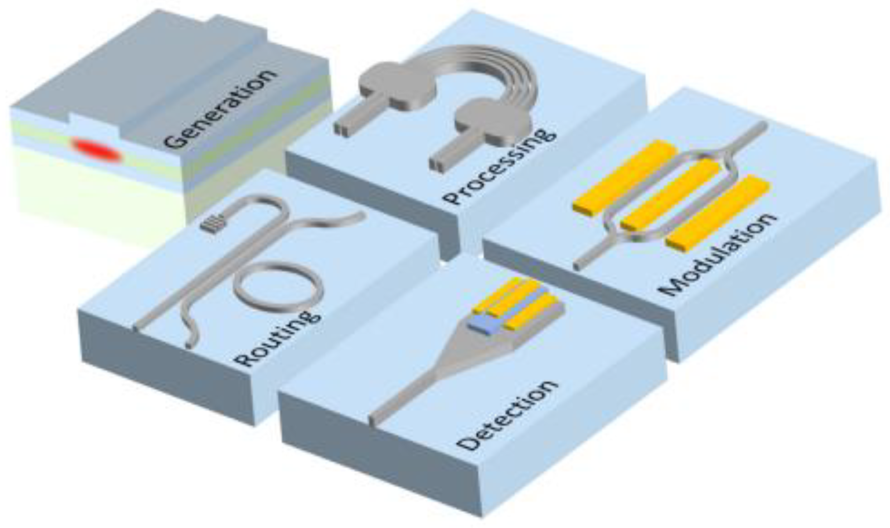
Figure 2.
The proposed Ge-on-Si photodiode using double lateral optical waveguides [5]. (a) Side view of the photodiode, (b) Top view of the PD, (c) Cross-sectional view of the PD, and (d) Electric field distribution across the waveguides, and along the Ge absorbing medium.
Figure 2.
The proposed Ge-on-Si photodiode using double lateral optical waveguides [5]. (a) Side view of the photodiode, (b) Top view of the PD, (c) Cross-sectional view of the PD, and (d) Electric field distribution across the waveguides, and along the Ge absorbing medium.
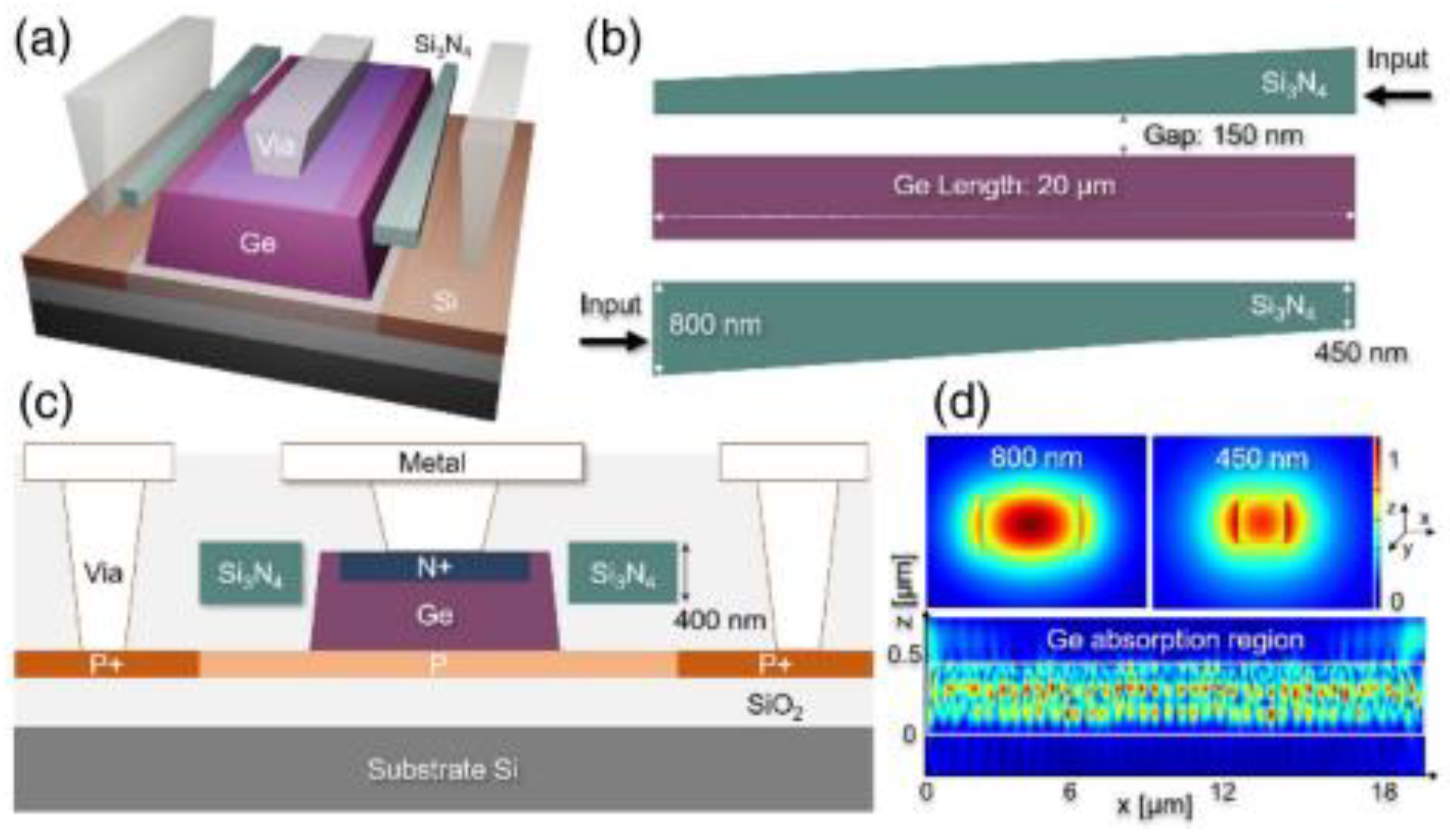
Figure 3.
(a) Butt-coupled PD with long taper. (b) The proposed mode-evolution-based coupled PD [7]. (c) The cross-section view of the proposed PD. (d) The top view of the proposed PD. (e) The optical generation rate for the butt-coupled PD. (f) The optical generation rate for the proposed mode-evolution-based coupled PD.

Figure 4.
(a) The proposed travelling-wave PD array in [10]. (b) The signal metal connections to the single-element PDs at B position. (c) The ground metal connections to the single-element PDs at C position.
Figure 4.
(a) The proposed travelling-wave PD array in [10]. (b) The signal metal connections to the single-element PDs at B position. (c) The ground metal connections to the single-element PDs at C position.
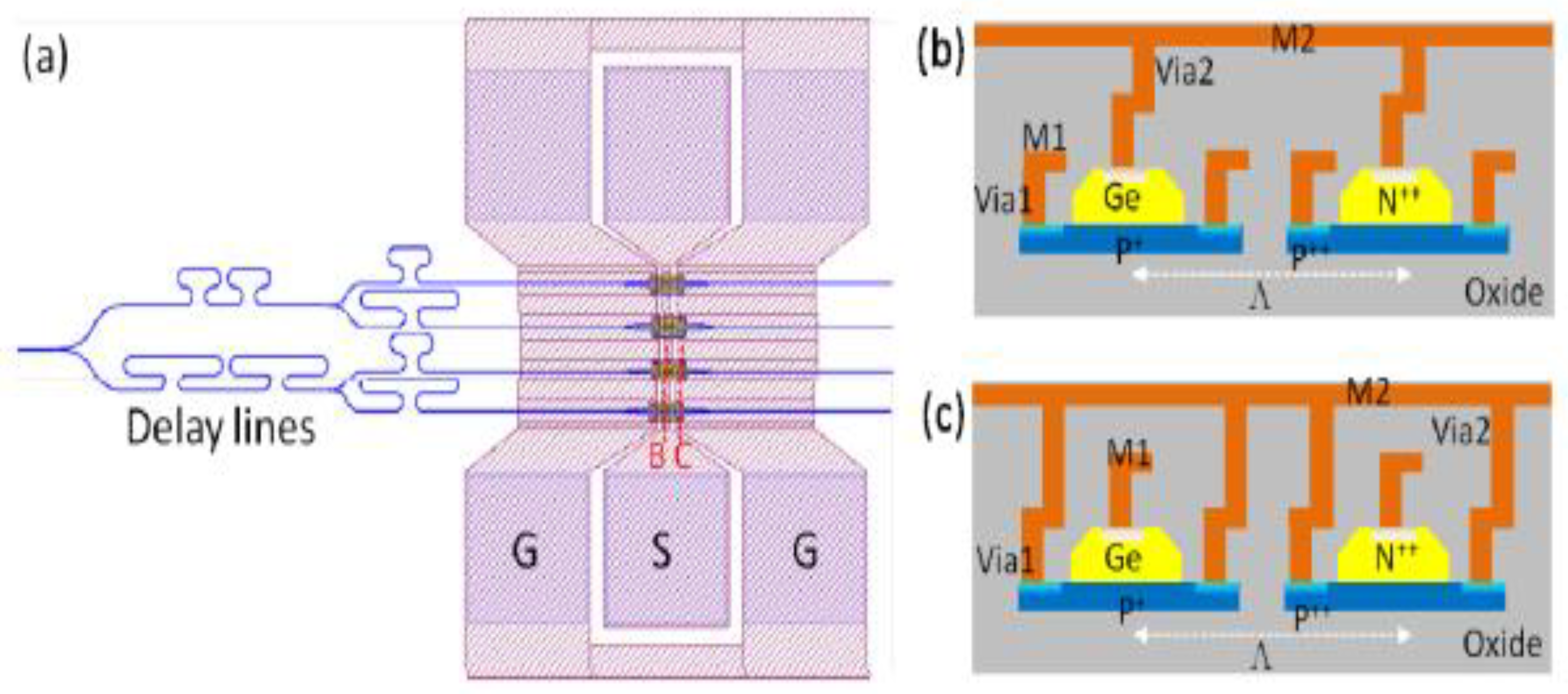
Figure 5.
The proposed High-Power and High-Speed dual-illuminated TWPDA in [11].
Figure 5.
The proposed High-Power and High-Speed dual-illuminated TWPDA in [11].
Figure 6.
(a) The incident light is split into two light beams to feed the proposed PD. (b) The proposed dual-injection PD in [25].
Figure 6.
(a) The incident light is split into two light beams to feed the proposed PD. (b) The proposed dual-injection PD in [25].
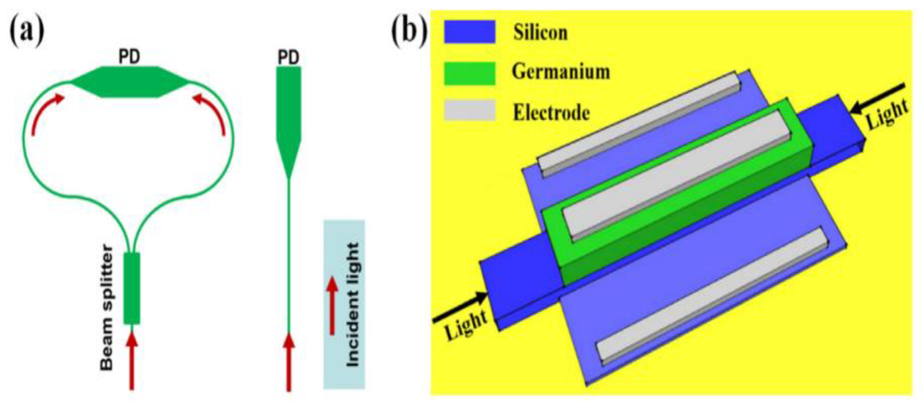
Figure 7.
(a) The 3D view of the proposed doping regulated PD in [15]. (b) The PD with conventional doping regions. (c) The PD with the optimized doping regions.
Figure 7.
(a) The 3D view of the proposed doping regulated PD in [15]. (b) The PD with conventional doping regions. (c) The PD with the optimized doping regions.
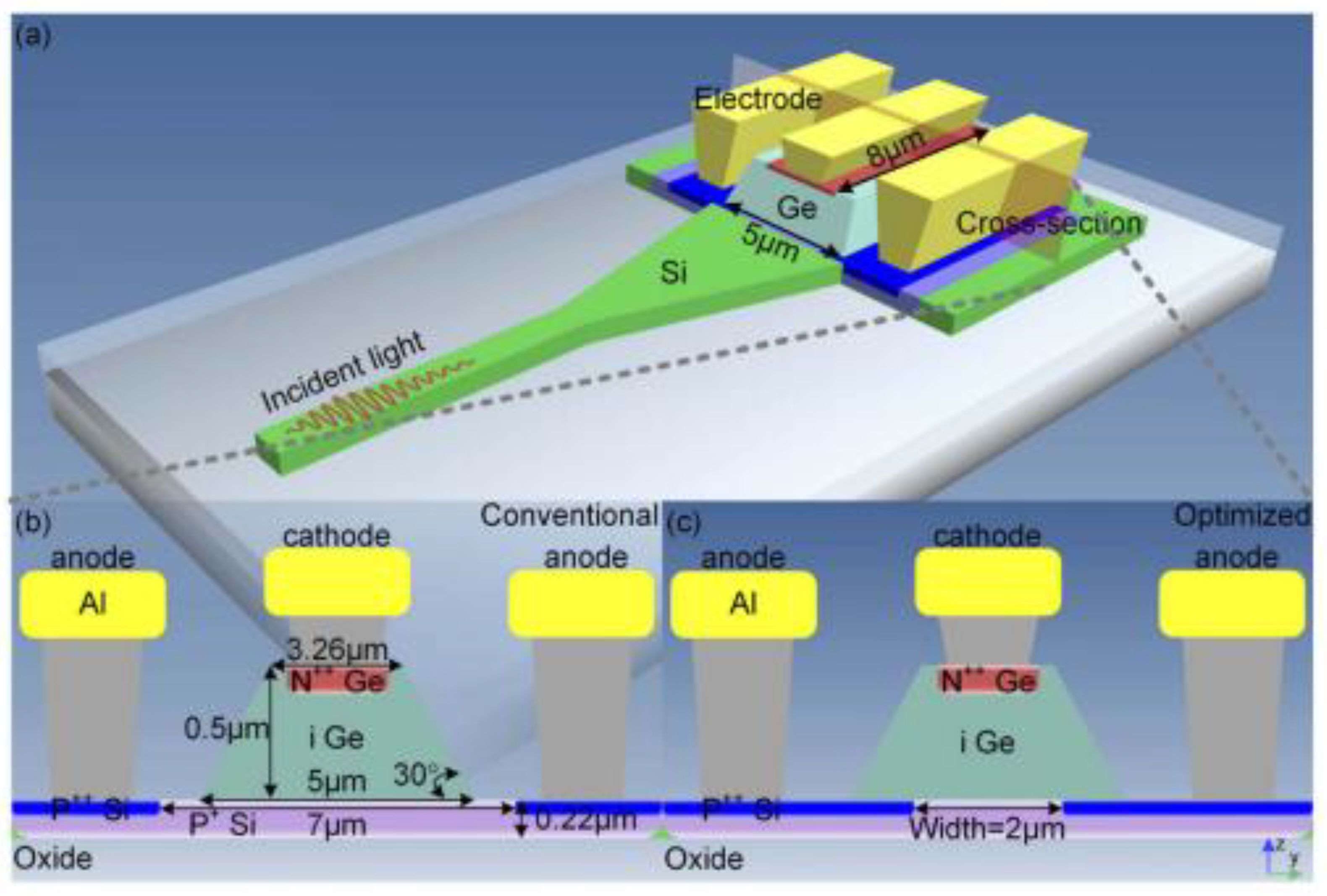
Figure 8.
(a) The proposed APD design in [23]. (b) The proposed absorption and charge multiplication region.
Figure 8.
(a) The proposed APD design in [23]. (b) The proposed absorption and charge multiplication region.
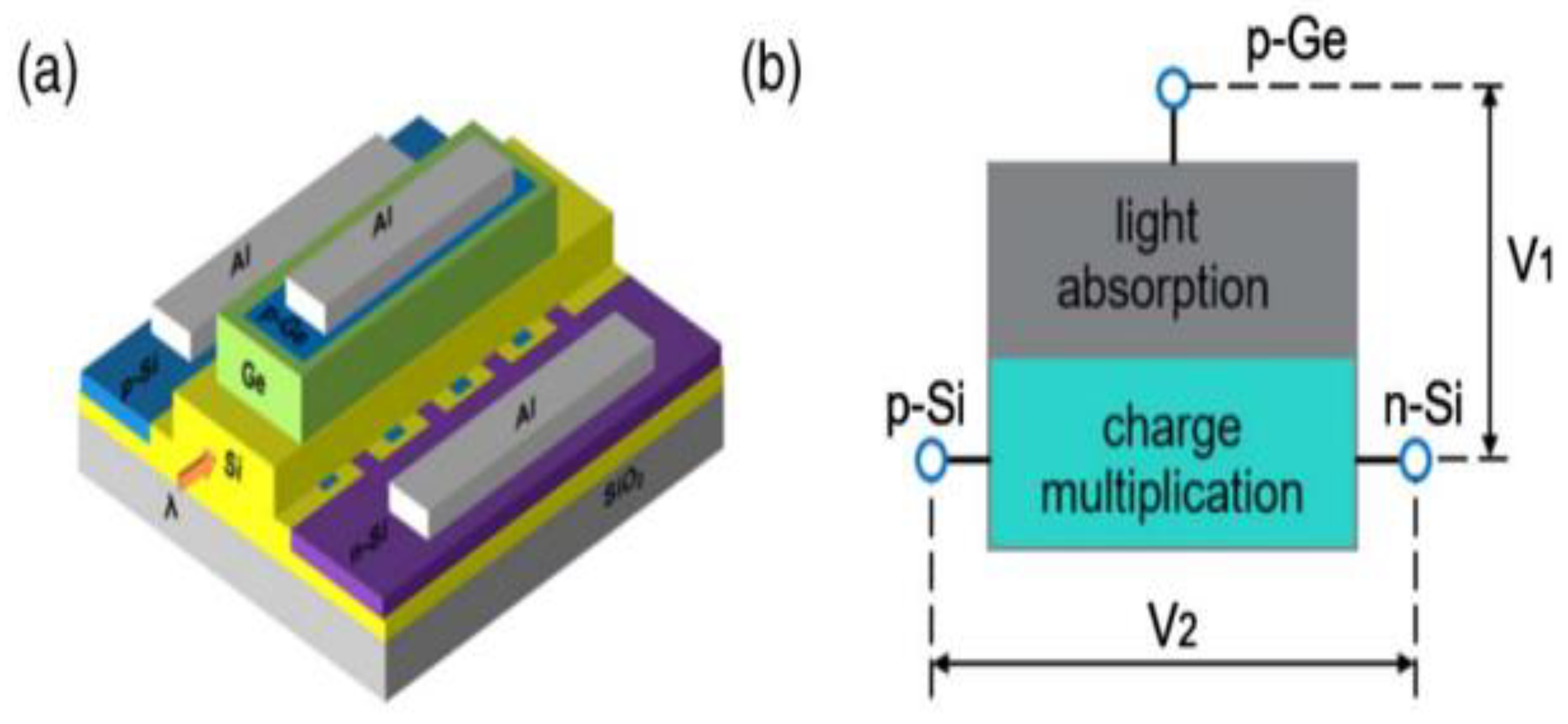
Figure 9.
The RC equivalent circuit for the Ge-on-Si PD in [5].
Figure 9.
The RC equivalent circuit for the Ge-on-Si PD in [5].
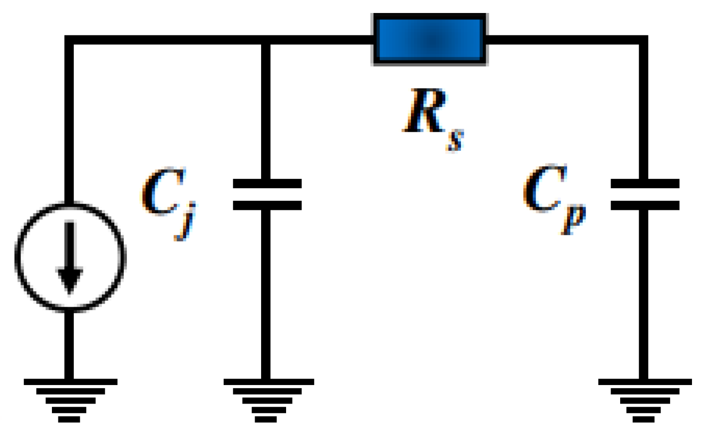
Figure 10.
The equivalent circuit of the proposed UTC PD in [18].
Figure 10.
The equivalent circuit of the proposed UTC PD in [18].
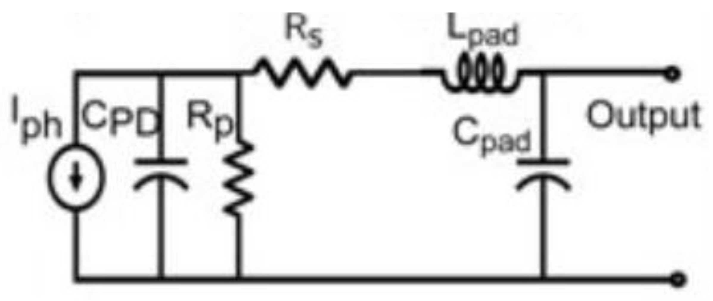
Figure 11.
The photodiode equivalent circuit including the transit time and the RC time effects [30].
Figure 11.
The photodiode equivalent circuit including the transit time and the RC time effects [30].
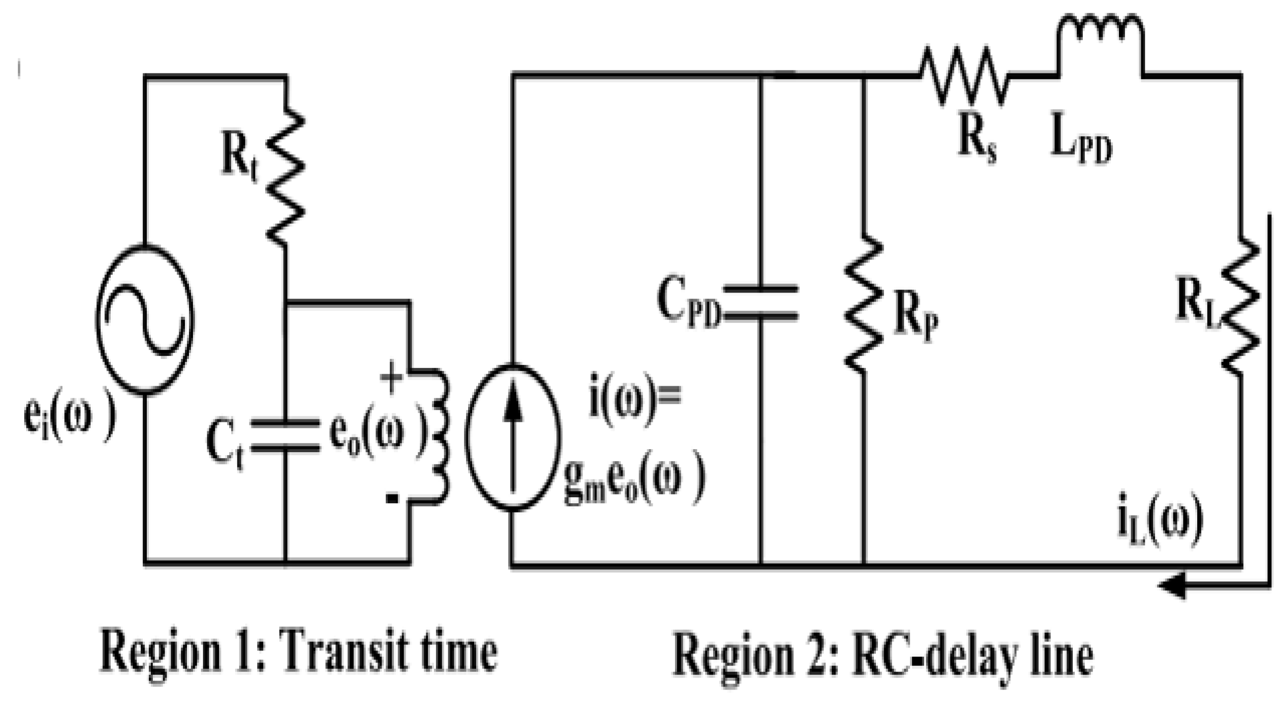
Figure 12.
The more accurate PD equivalent circuit including the full-wave simulated PD CPW pads, as was proposed in [31].
Figure 12.
The more accurate PD equivalent circuit including the full-wave simulated PD CPW pads, as was proposed in [31].
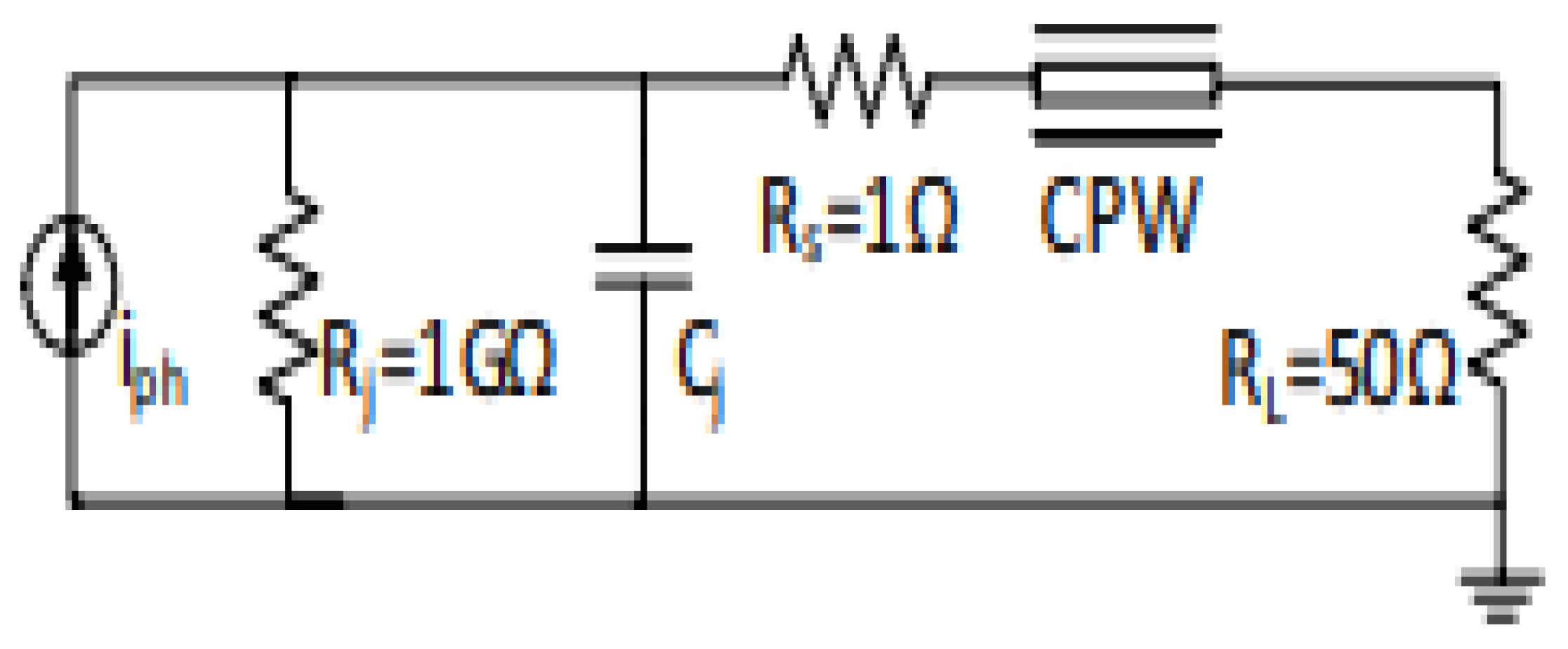
Figure 13.
The PD equivalent circuit including the simulated S-parameters of the PD CPW pads [32].
Figure 13.
The PD equivalent circuit including the simulated S-parameters of the PD CPW pads [32].
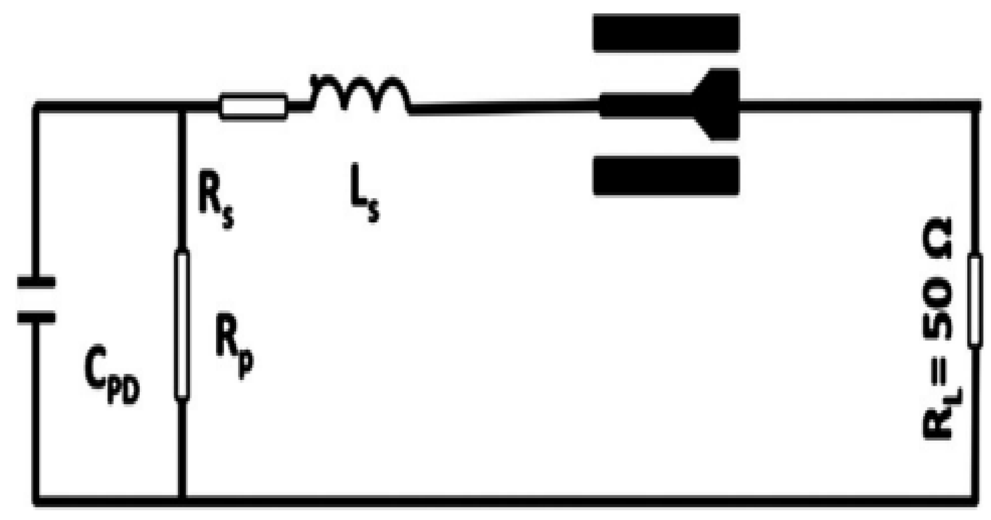
Figure 14.
The RC equivalent circuit for the PD array proposed in [7].
Figure 14.
The RC equivalent circuit for the PD array proposed in [7].
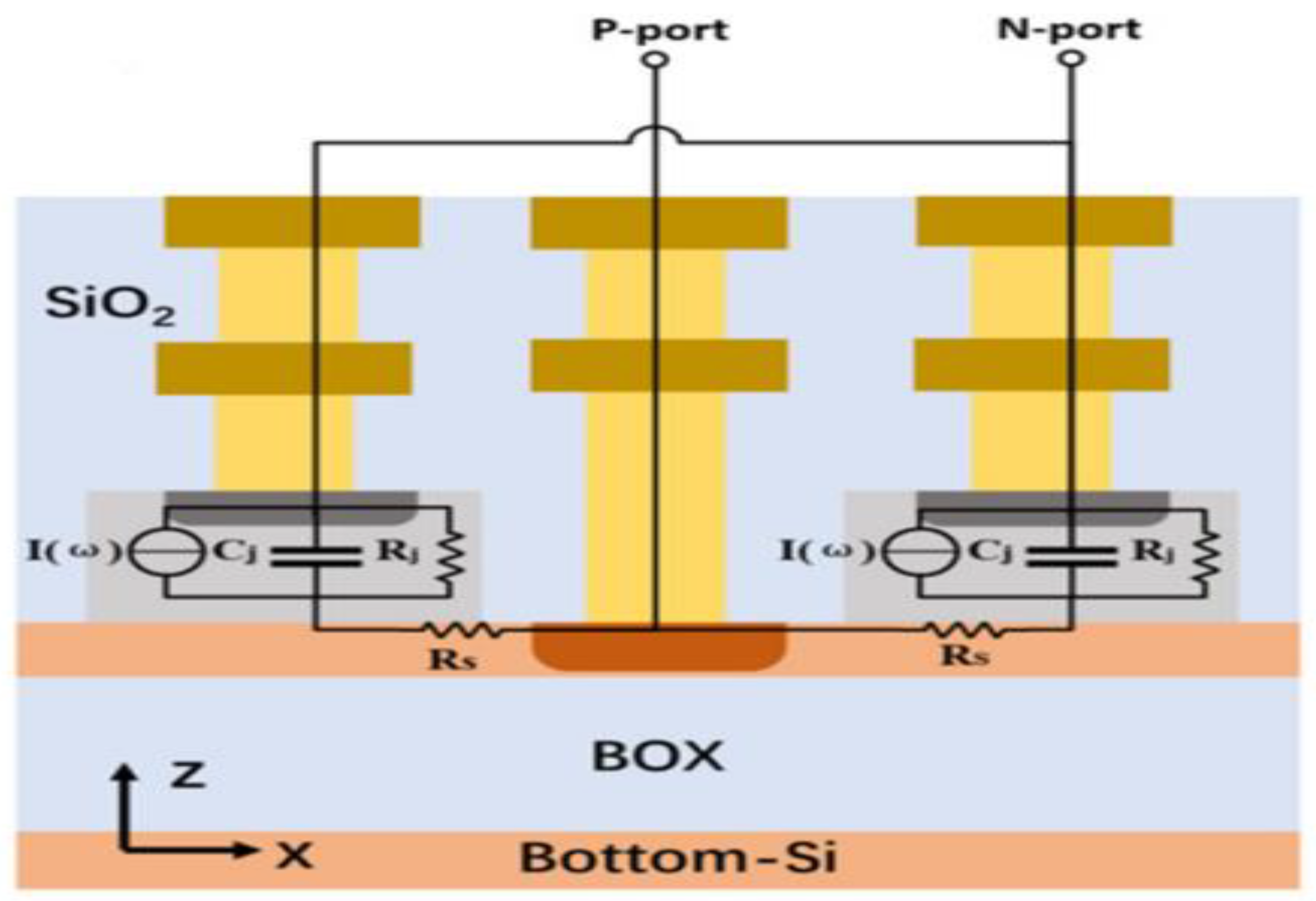
Figure 15.
(a) The equivalent circuit for a single-element PD. (b) The equivalent circuit for a two-element PD array [8].
Figure 15.
(a) The equivalent circuit for a single-element PD. (b) The equivalent circuit for a two-element PD array [8].
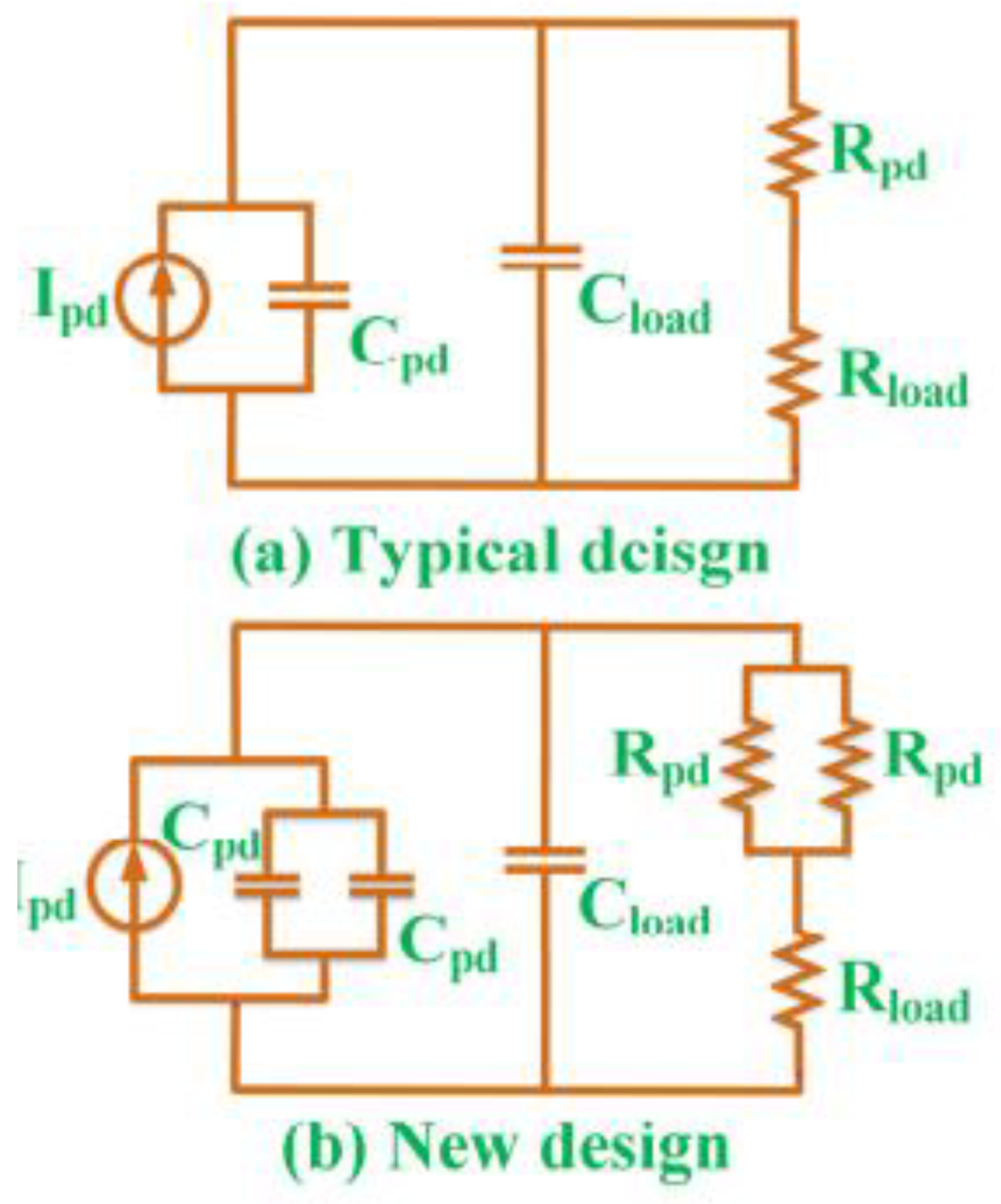
Figure 16.
The equivalent circuit for the proposed n-element PD array in [9].
Figure 16.
The equivalent circuit for the proposed n-element PD array in [9].
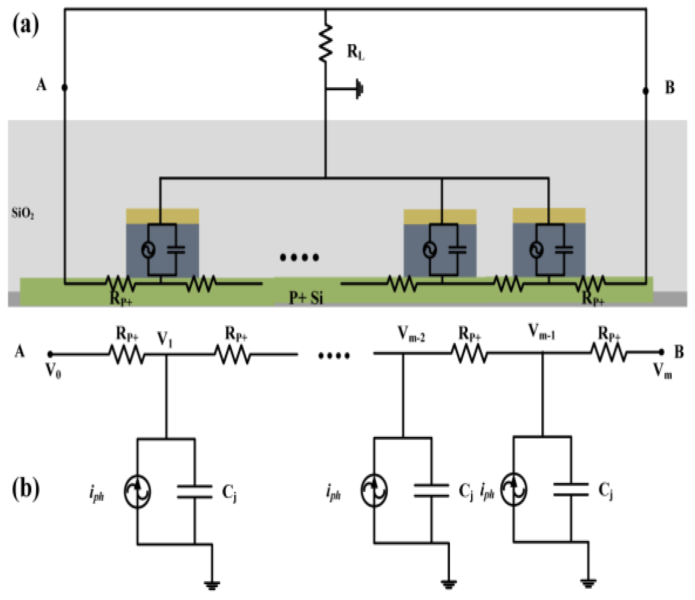
Figure 17.
The proposed photocurrent versus optical power characteristics for the proposed PD in [25].
Figure 17.
The proposed photocurrent versus optical power characteristics for the proposed PD in [25].
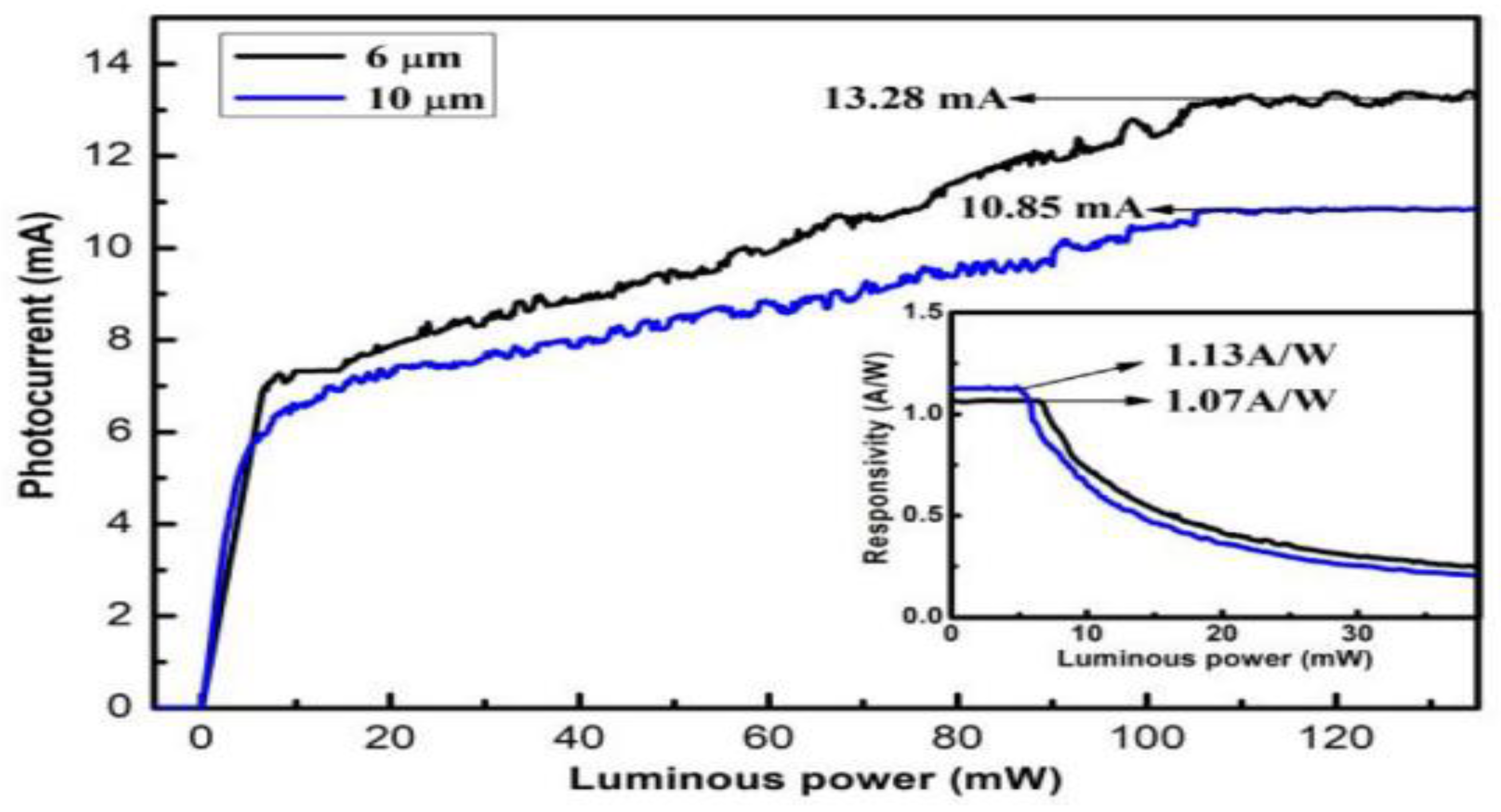
Figure 18.
Different optical field manipulation techniques, proposed in [26].
Figure 18.
Different optical field manipulation techniques, proposed in [26].
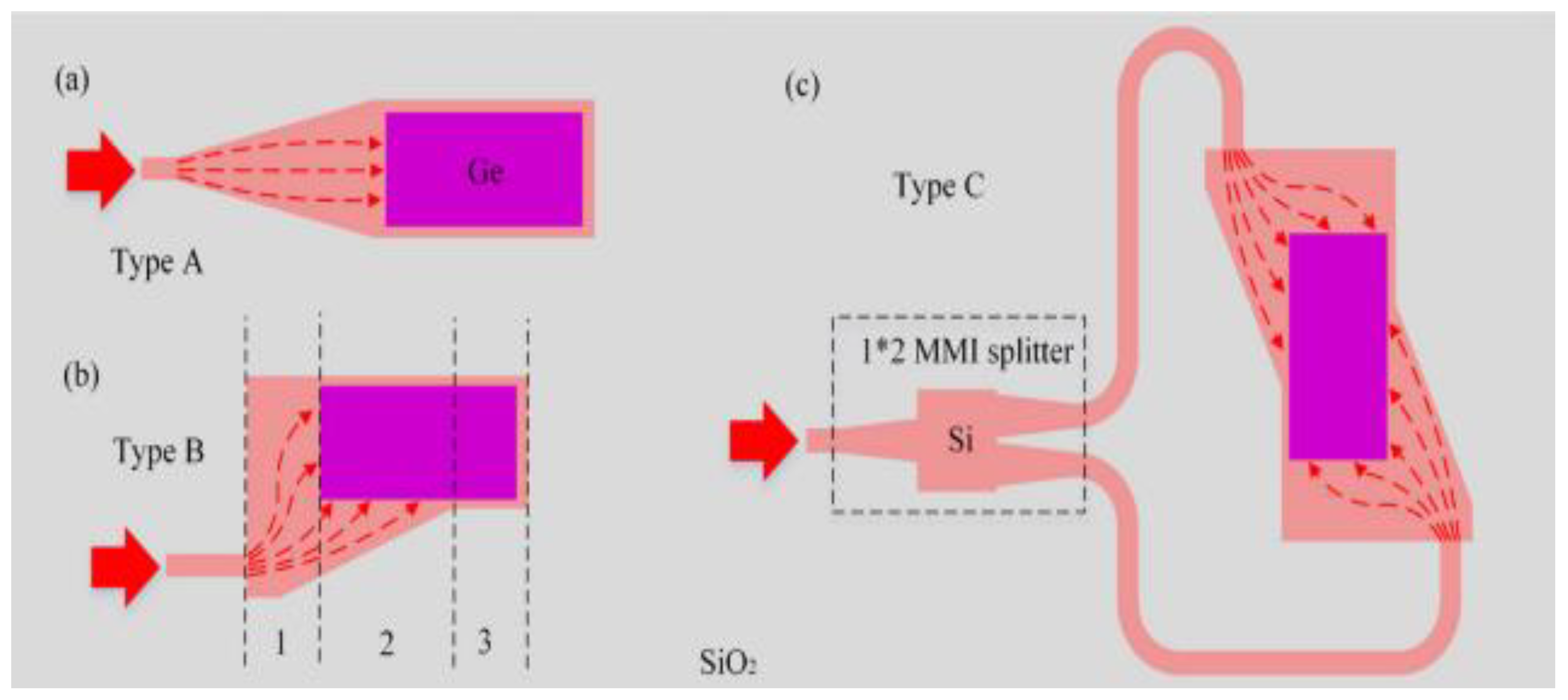
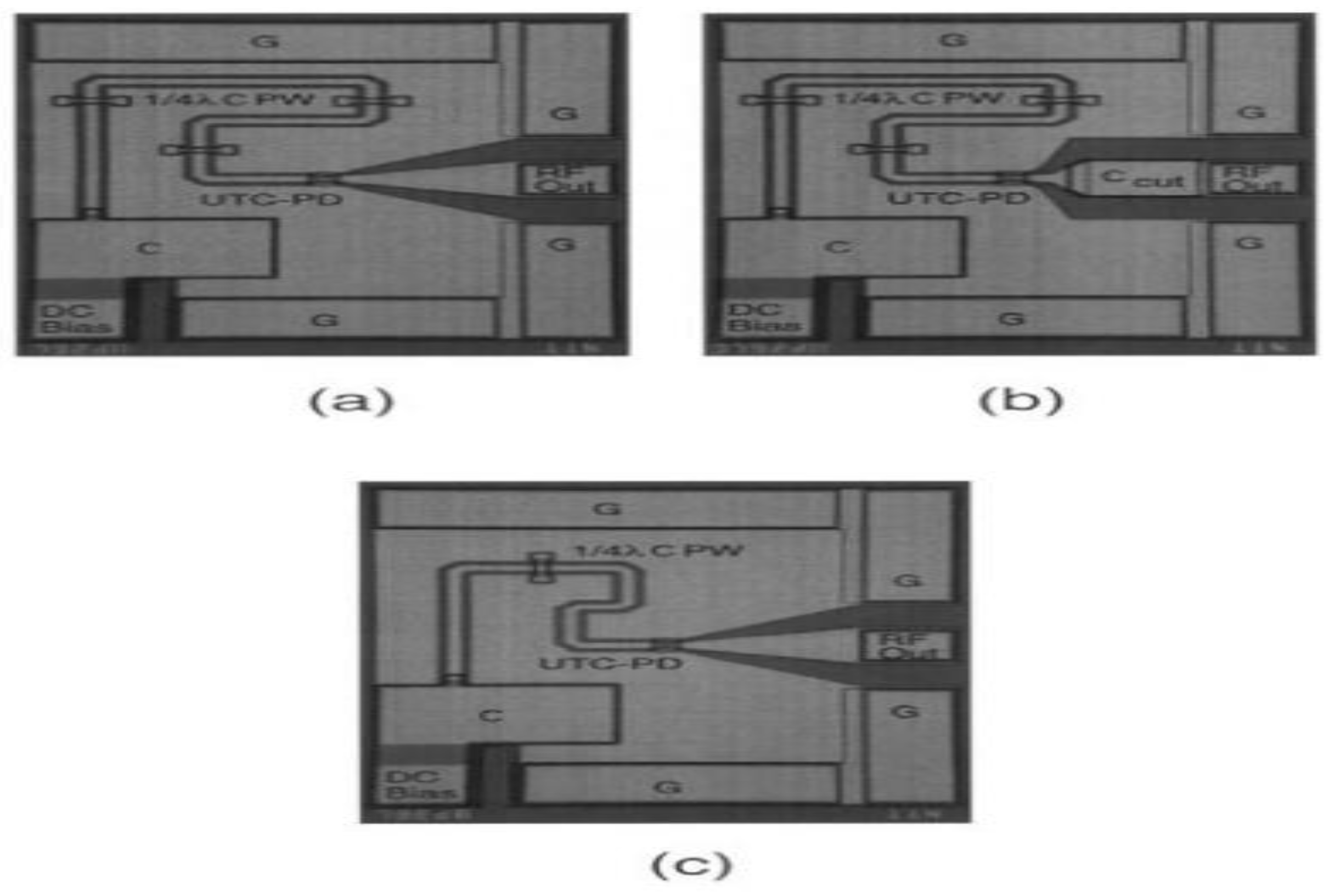
Figure 20.
The proposed circuit model for the photonic-integrated connected array antenna in [38].
Figure 20.
The proposed circuit model for the photonic-integrated connected array antenna in [38].
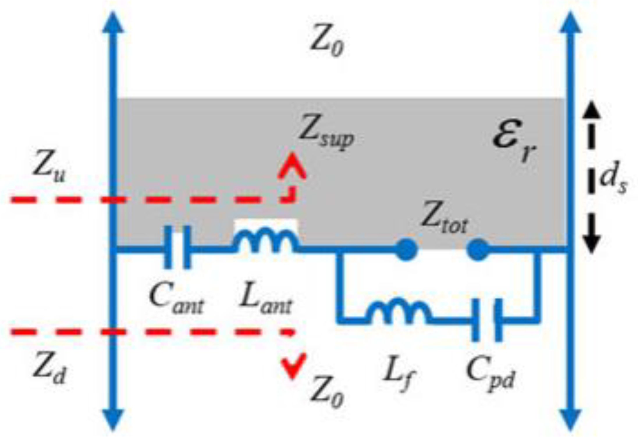
Figure 21.
The proposed photonic-integrated SAID antenna proposed in [39].
Figure 21.
The proposed photonic-integrated SAID antenna proposed in [39].
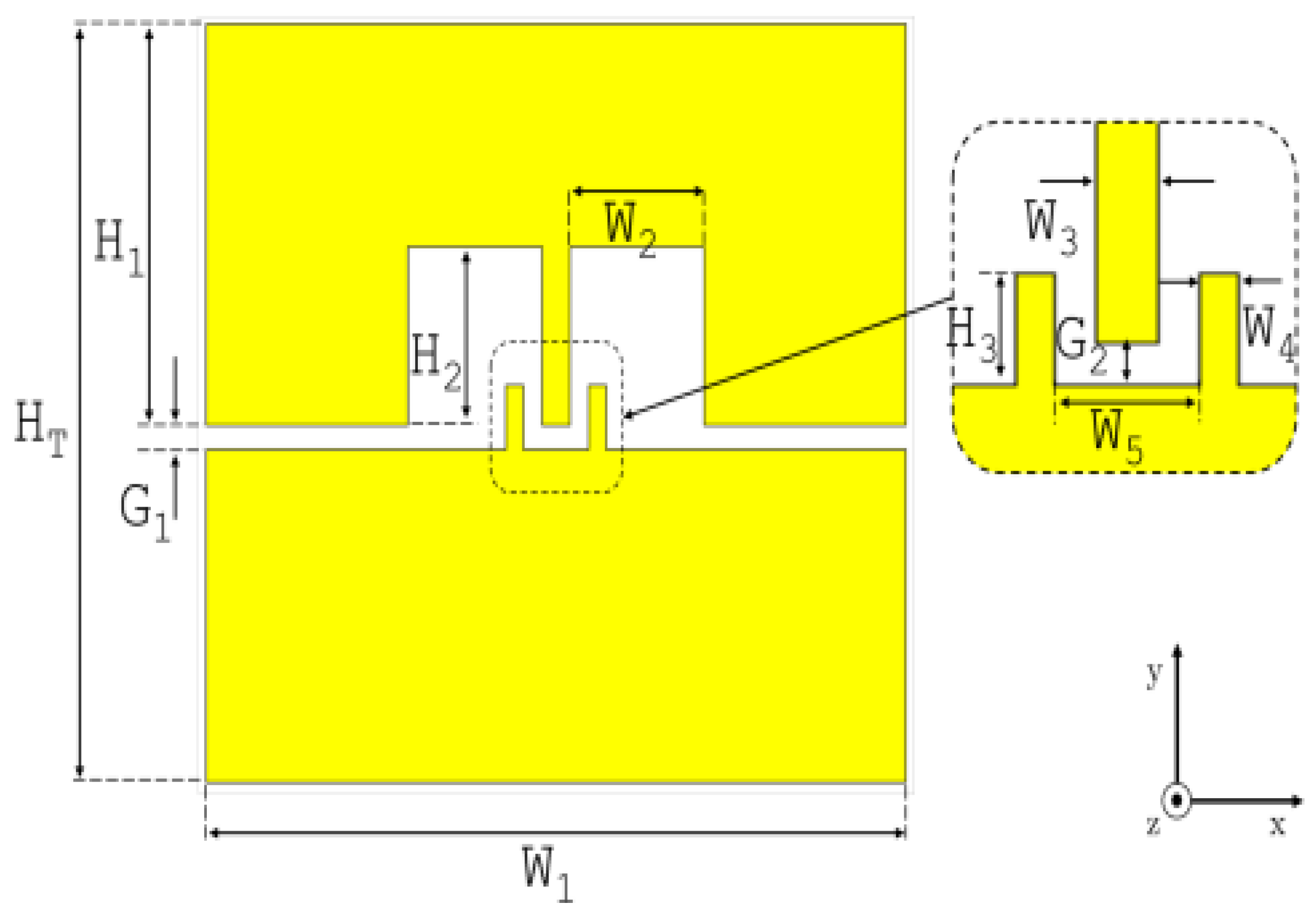
Figure 22.
The proposed trans-impedance low-noise amplifier in [40].
Figure 22.
The proposed trans-impedance low-noise amplifier in [40].
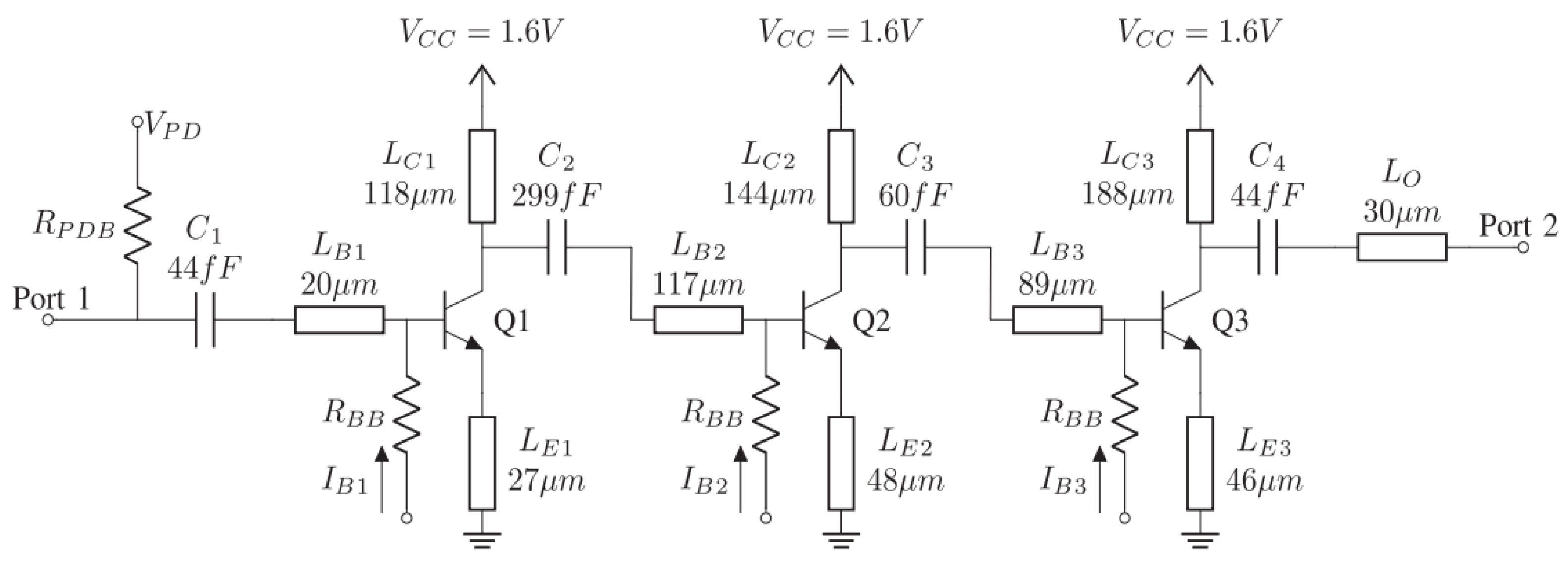
Figure 23.
The proposed GCPW bias-tee in [41].
Figure 23.
The proposed GCPW bias-tee in [41].
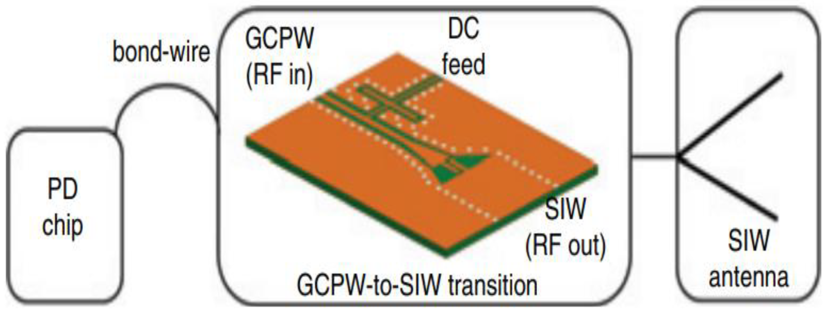
Figure 24.
The proposed GCPW bias-tee in [42].
Figure 24.
The proposed GCPW bias-tee in [42].
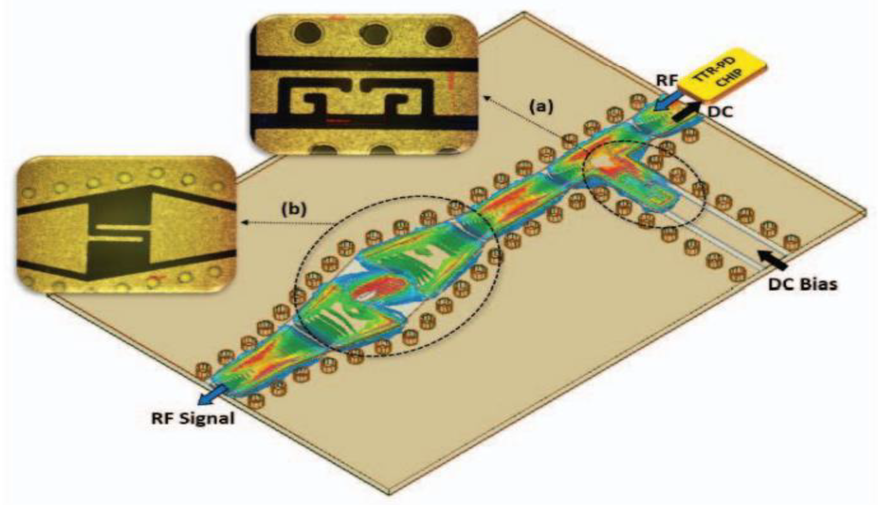
Figure 25.
The proposed SiPh monopole antenna in [43].
Figure 25.
The proposed SiPh monopole antenna in [43].
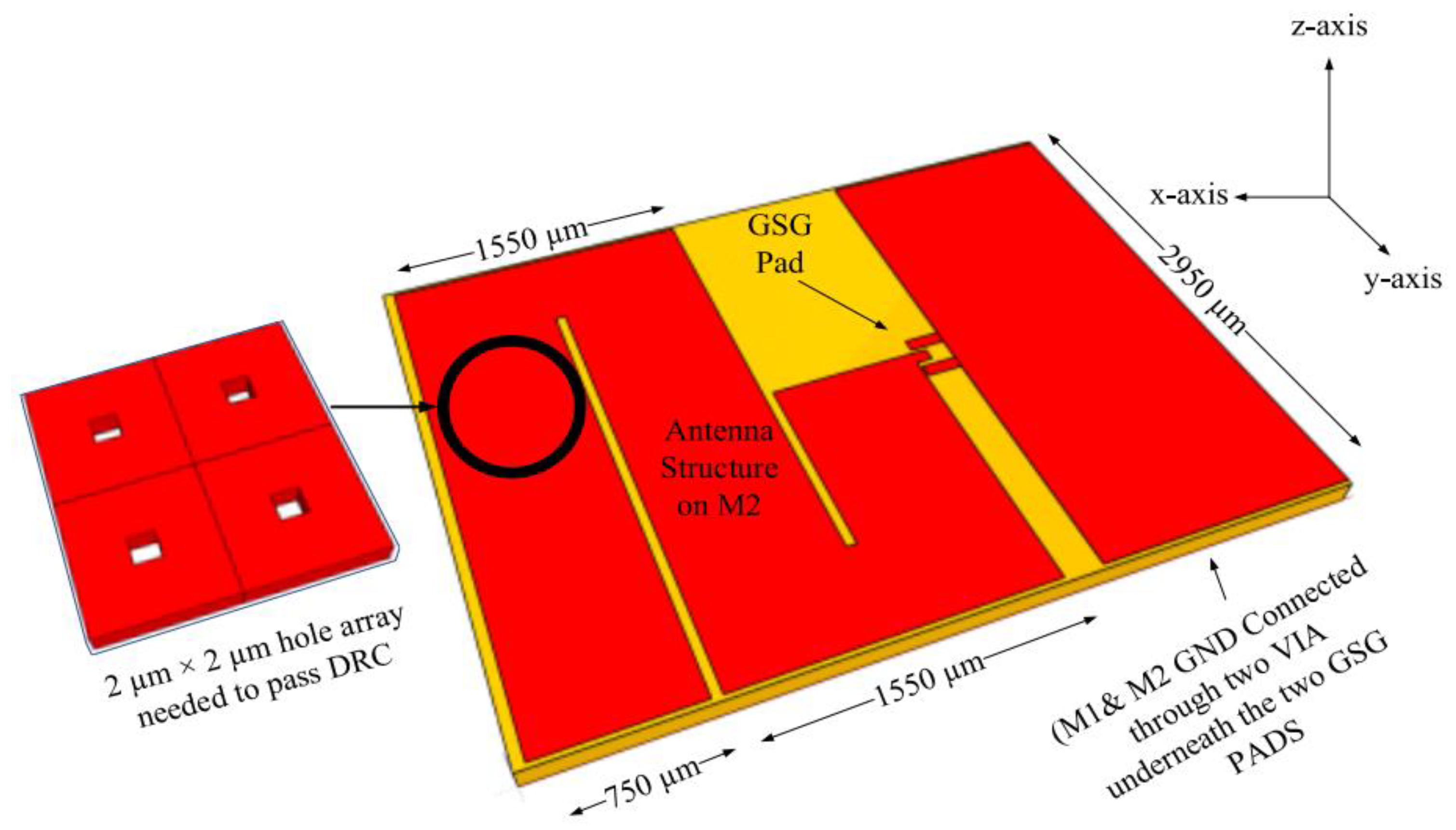
Figure 26.
The proposed photonic-integrated slot antenna in [45]. (a) The photonic integrated single-element slot antenna. (b) The equivalent circuit for the single-element slot antenna. (c) The conjugate-matched single-element photonic antenna. (d) Equivalent circuit of the conjugate-matched single-element antenna. (e) The photonic antenna array with four elements, and an image for the active array.
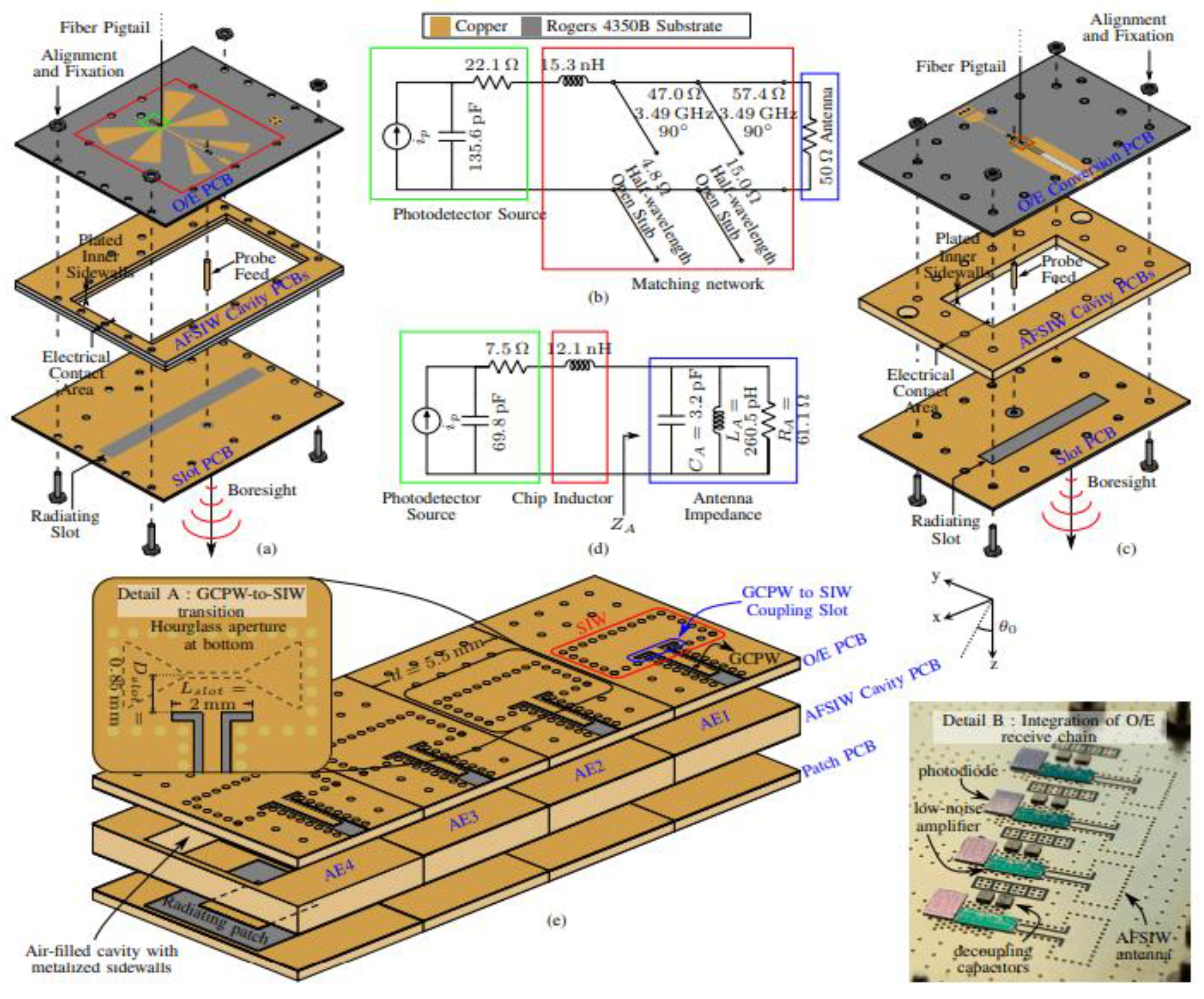
Figure 27.
The proposed short asymmetrical inductive dipole antenna in [48].
Figure 27.
The proposed short asymmetrical inductive dipole antenna in [48].
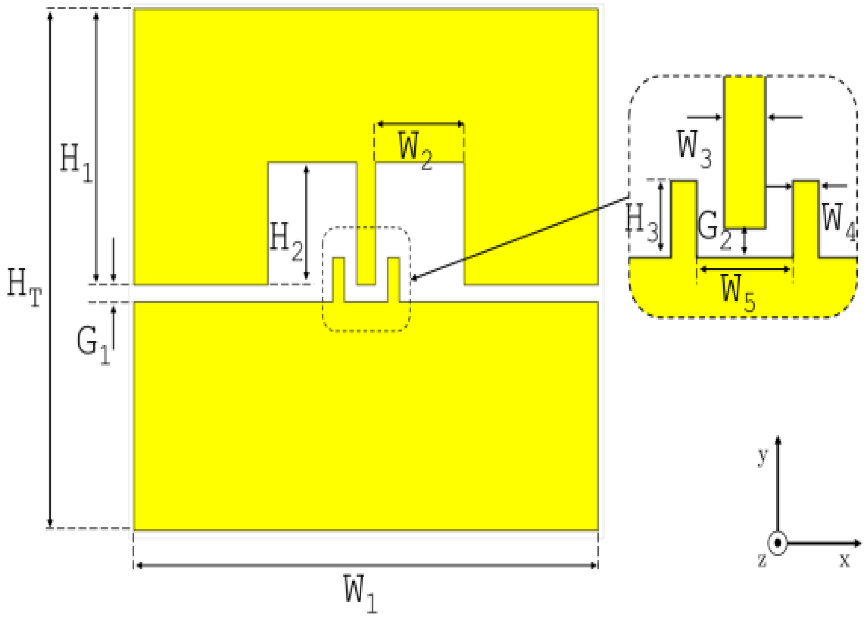
Figure 28.
(a) The top view of the proposed photonic modulated MTS array antenna in [46]. (b) The proposed four modulated MTS subarrays.
Figure 28.
(a) The top view of the proposed photonic modulated MTS array antenna in [46]. (b) The proposed four modulated MTS subarrays.
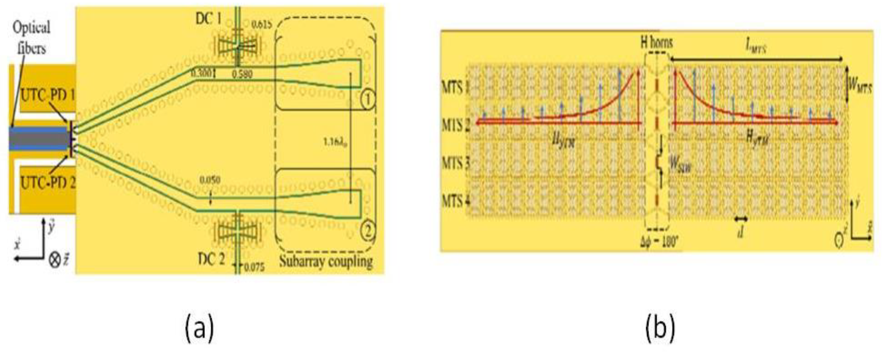
Figure 29.
The proposed photonic-integrated subarray antenna in [47].
Figure 29.
The proposed photonic-integrated subarray antenna in [47].
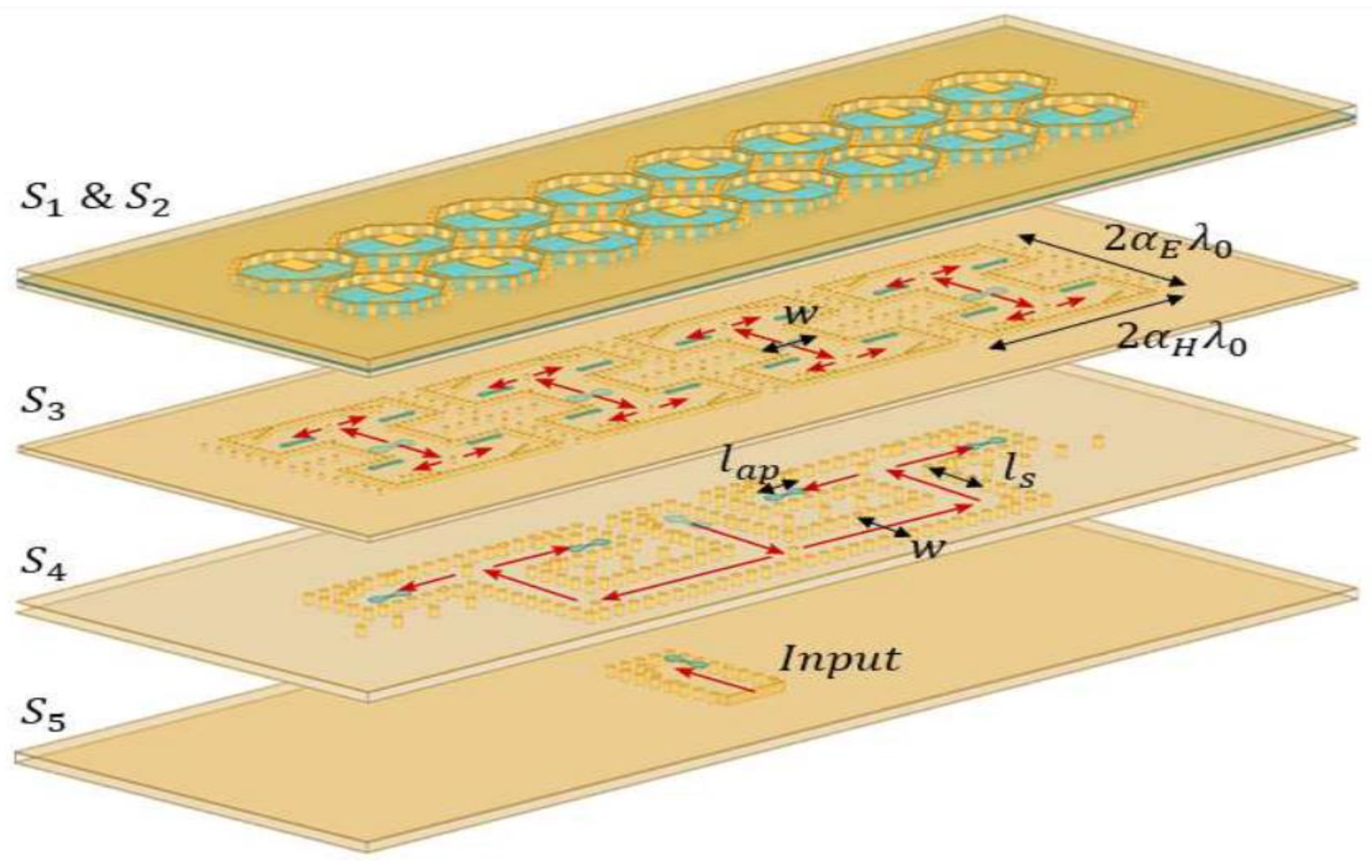
Figure 30.
The proposed LWA array in [49], and the unit-cell of the radiating section.
Figure 30.
The proposed LWA array in [49], and the unit-cell of the radiating section.
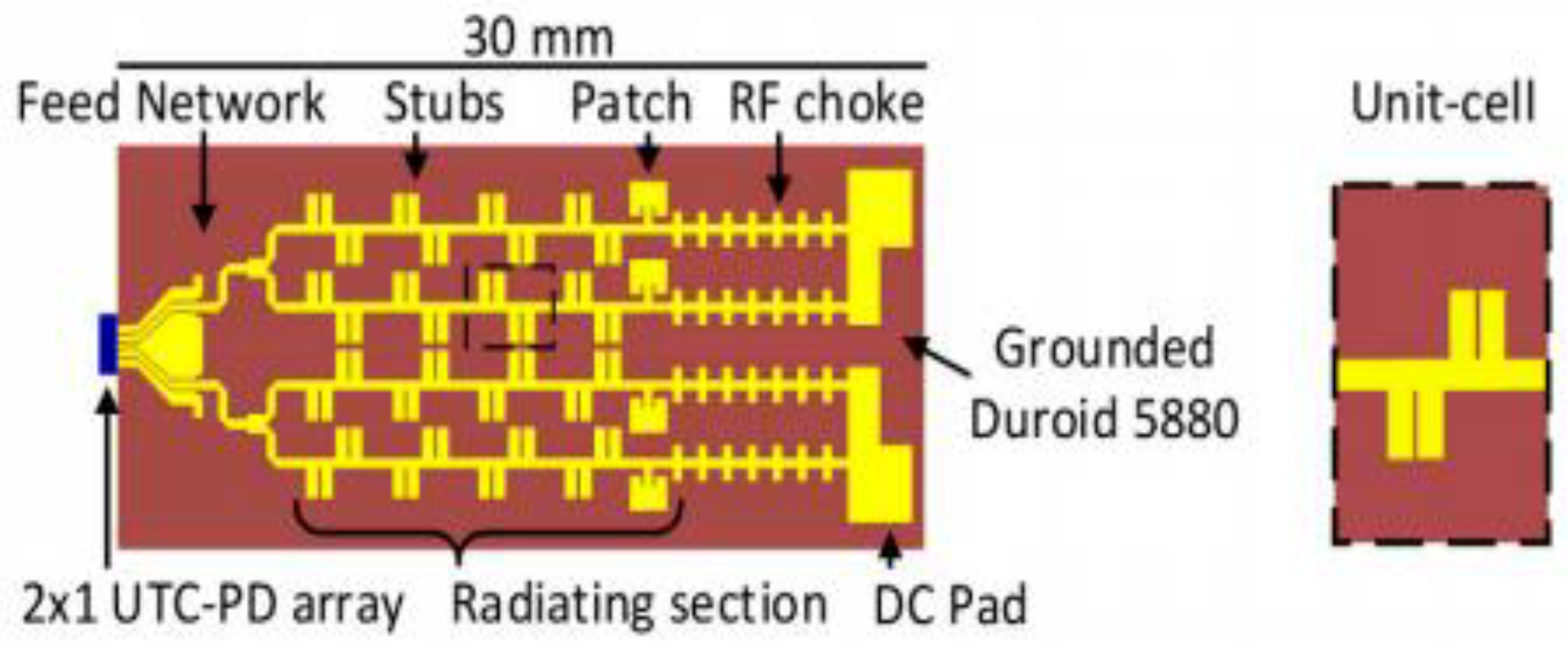
Figure 31.
The proposed photonic-integrated antenna array proposed in [50].
Figure 31.
The proposed photonic-integrated antenna array proposed in [50].
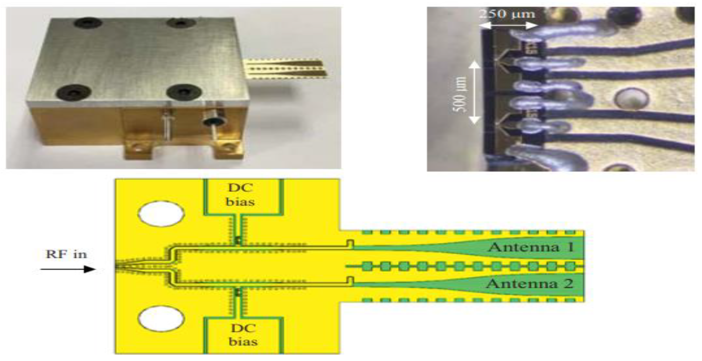
Figure 32.
The proposed CA antenna in [38] with four single mode fibers and lens connected to the active antenna elements.
Figure 32.
The proposed CA antenna in [38] with four single mode fibers and lens connected to the active antenna elements.
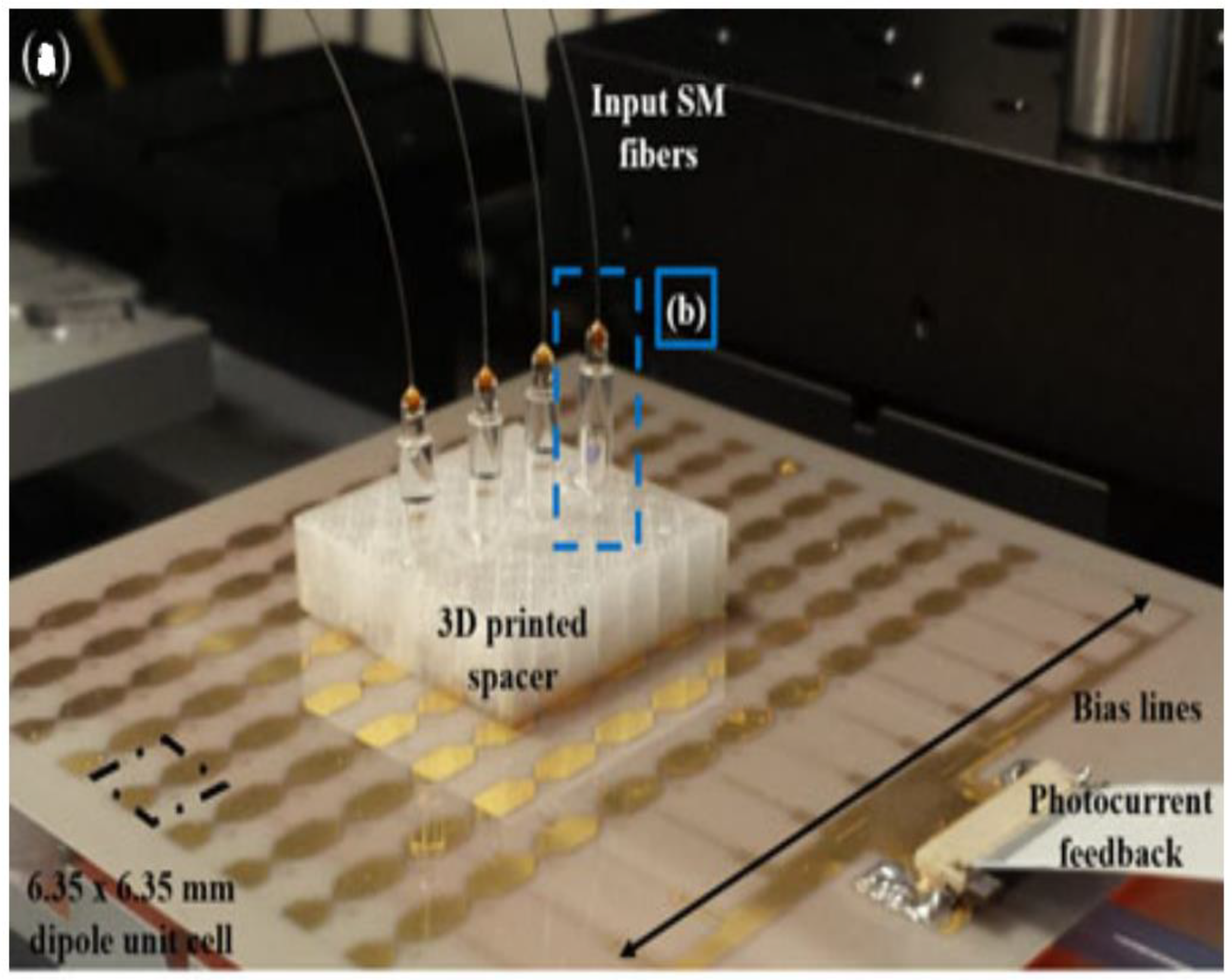
Figure 33.
The proposed photonic coplanar patch in [53].
Figure 33.
The proposed photonic coplanar patch in [53].
Disclaimer/Publisher’s Note: The statements, opinions and data contained in all publications are solely those of the individual author(s) and contributor(s) and not of MDPI and/or the editor(s). MDPI and/or the editor(s) disclaim responsibility for any injury to people or property resulting from any ideas, methods, instructions or products referred to in the content. |
© 2025 by the authors. Licensee MDPI, Basel, Switzerland. This article is an open access article distributed under the terms and conditions of the Creative Commons Attribution (CC BY) license (http://creativecommons.org/licenses/by/4.0/).
Copyright: This open access article is published under a Creative Commons CC BY 4.0 license, which permit the free download, distribution, and reuse, provided that the author and preprint are cited in any reuse.


