Submitted:
22 April 2025
Posted:
25 April 2025
You are already at the latest version
Abstract
We propose 24 modifications of buffer amplifiers for use as output stages in micropower operational amplifiers, designed for the SiGe BiCMOS technological process. This process enables the fabrication of heterojunction n-p-n bipolar transistors and n- and p-channel CMOS transistors. A cataloging and visualization program has been developed for the analyzed circuits, which differ in parameters such as input/output resistances, quiescent current consumption, biasing network design, maximum positive/negative output voltage amplitudes, etc. An example of computer simulation results for static operating points and amplitude characteristics in Cadence is provided at two temperatures: 27°C and 250°C. The proposed circuit solutions are recommended for applications in various analog microelectronic devices operating under high-temperature conditions.
Keywords:
high-temperature electronics
; analog interfaces
; operational amplifiers
; output stages
; buffer amplifiers
; SiGe
; BiCMOS
Introduction
One of the most significant technological breakthroughs in the electronics world at the end of the 20th century was the development of a new process technology – SiGe BiCMOS (Bipolar Complementary Metal-Oxide-Semiconductor), which combines the advantages of high-speed bipolar transistors and CMOS- structures. This process technology [1,2,3,4,5,6,7,8] serves as the foundation for creating electronic components for system-on-chip solutions, which have become the basis for a new generation of devices and telecommunications equipment (radar systems, cellular and satellite communications, navigation systems, etc.). Originally developed by IBM, this technology is now widely used worldwide and continues to evolve, with leading microelectronics companies such as Intel, Intersil, Motorola, Texas Instruments, and TSMC contributing to its advancement. The reason for its widespread adoption lies in its combination of high-performance characteristics, reliability comparable to conventional silicon-based devices, and cost-effectiveness. [9]
The purpose and novelty of this article is to summarize the fundamental properties and provide a comparative analysis of 24 modified SiGe BiCMOS output stages of operational amplifiers (Op-Amps) with an operating temperature range up to 250°C.
A cataloging and visualization program for OS of high-temperature Op-Amps based on heterojunction n-p-n bipolar and n- and p-channel metal-oxide-semiconductor field-effect transistors
To select the optimal circuit design solution for a specific Op-Amp implementation, a buffer amplifiers (BA) cataloging program was developed (Figure 1). This program represents an interactive platform containing electrical schematics adapted for SiGe technology processes, utilizing exclusively heterojunction n-p-n bipolar and CMOS transistors.
Figure 1.
Fragment of the BA cataloging and visualization program description file.

This program solves the following problems:
- cataloging of circuits with a description of their operation;
- graphical visualization of the selected circuit solution with displaying the numbering of components and their connections (as in Figure 2).
Figure 2.
Basic scheme information window.
Thus, the program as an effective tool for designers of high-temperature SiGe Op-Amps, enabling optimization of the output stage (BA) selection process while accounting for its circuit design characteristics.
Buffer amplifier circuits for high-temperature Op-Amps using heterojunction n-p-n bipolar and CMOS transistors, as implemented in the program
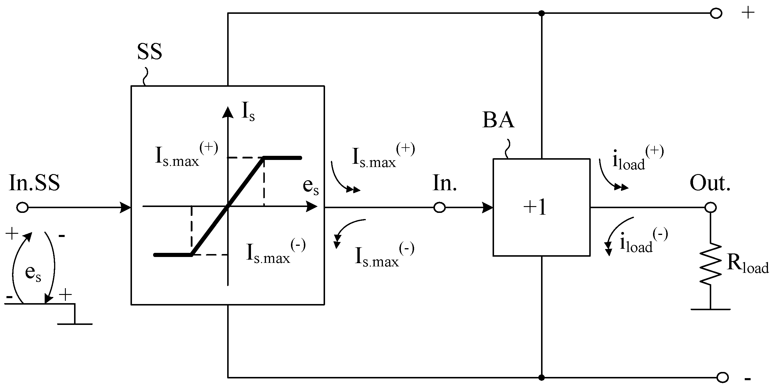
When calculating the maximum output currents of the BA ( and ) for the considered circuits, it should be taken into account that in real Op-Amps circuits, the signal source connected to the BA input (In.) is not an ideal voltage source with zero output impedance. Consequently, the separate stage (SS) limits the maximum possible load currents values. Therefore, when evaluating and for specific circuits (measured at Rload=0), the maximum possible output currents and of the separate stage SS must be taken into account. In Figure 3 shows a BA circuit with non-ideal SS signal source.
Figure 3.
On the operation of the BA with a non-ideal signal source SS.
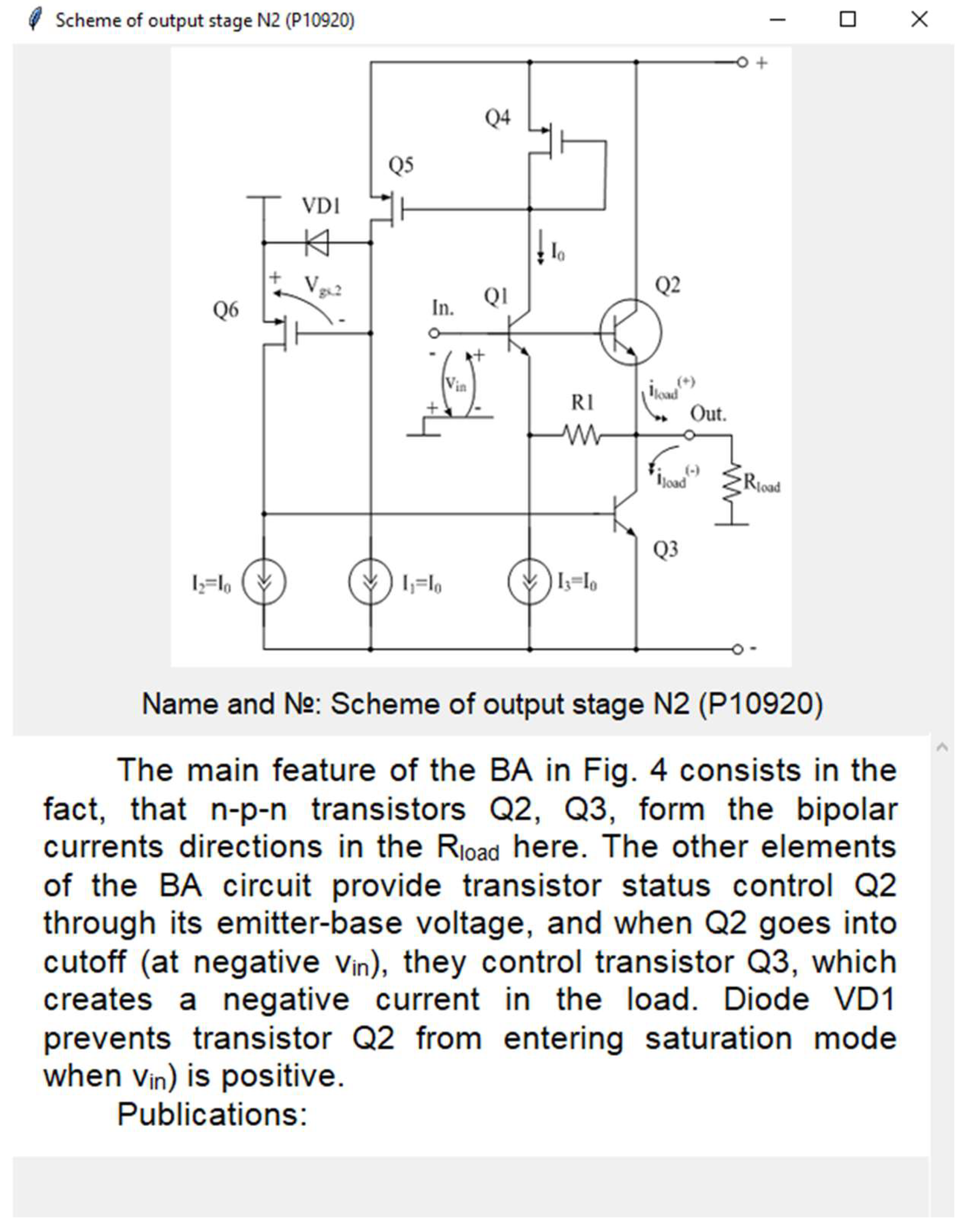
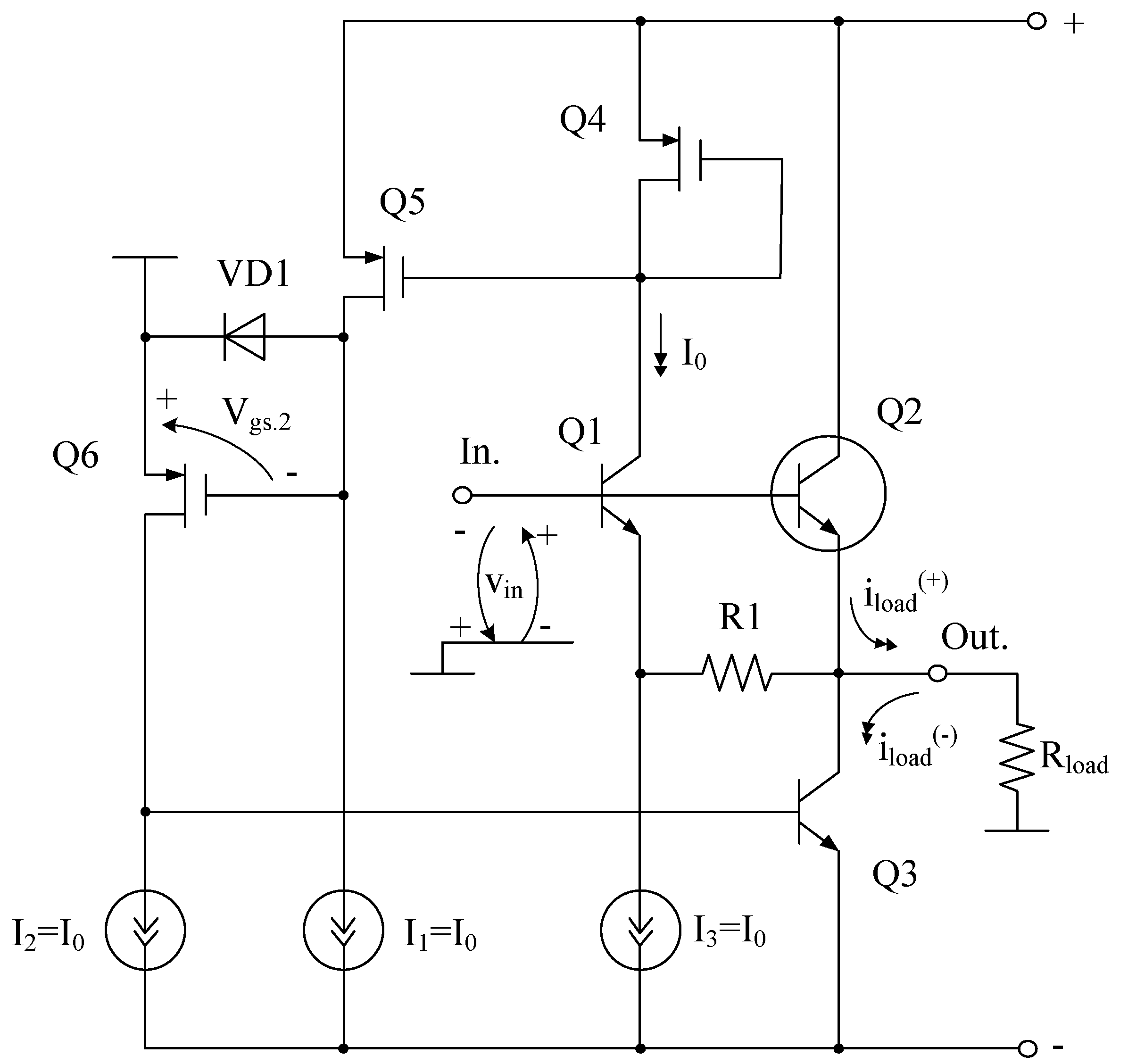
The main feature of the BA in Figure 4 consists in the fact, that n-p-n transistors Q2, Q3, form the bipolar currents directions in the Rload load here. The other elements of the BA circuit provide transistor status control Q2 through its emitter-base voltage, and when Q2 goes into cutoff (at negative vin), they control transistor Q3, which creates a negative current in the load. Diode VD1 prevents transistor Q2 from entering saturation mode when vin is positive.
Figure 4.
SiGe buffer amplifier: modification №1.
The setting of the BA circuit in Figure 4 is provided by selection of resistor R2 and currents I1=I2=I3. In this case, the maximum values of currents in the load and are determined by the formulas:
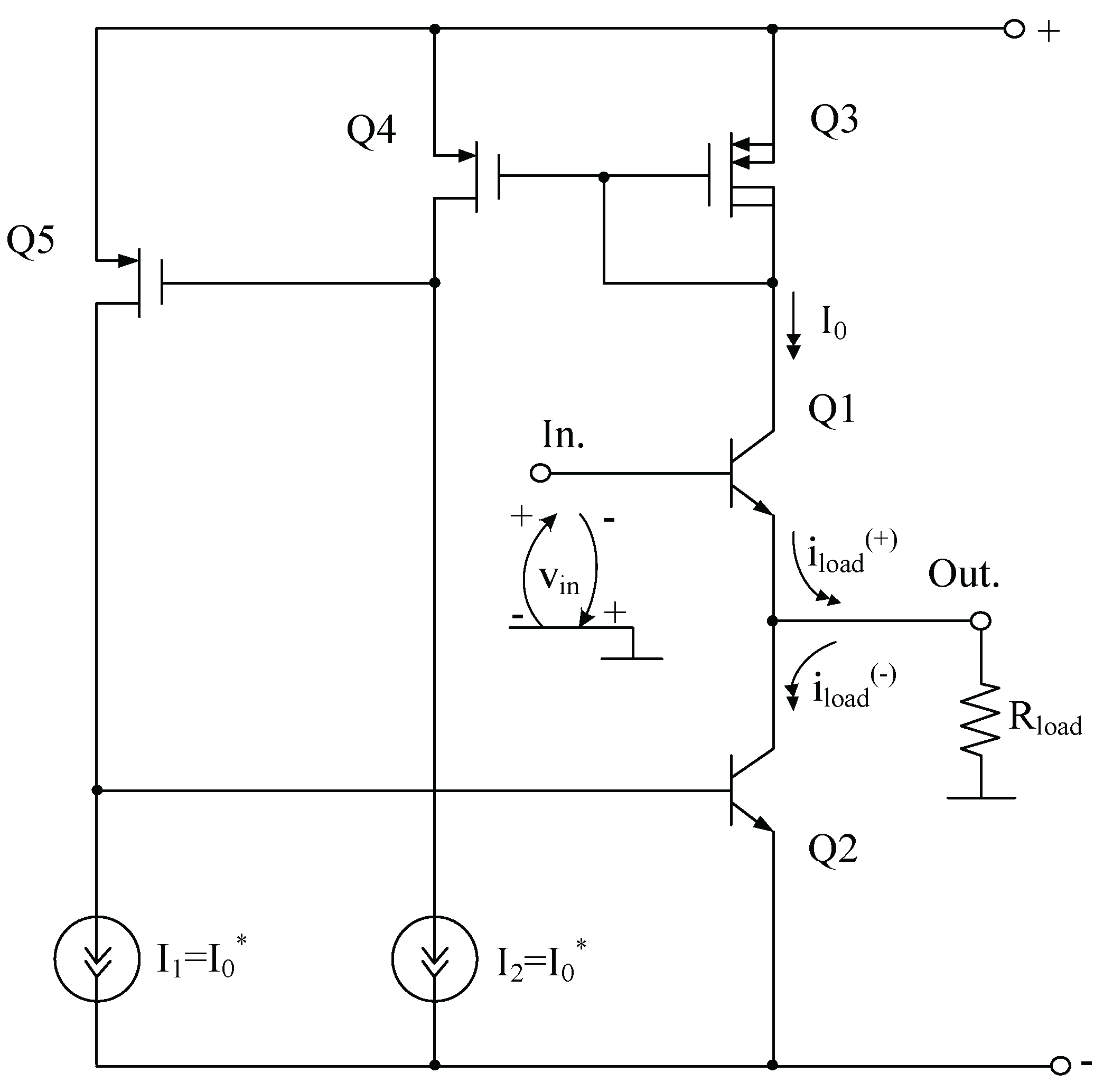
where – transistor base current gain Q2, – maximum possible value of SS (Figure 3) output current with positive vin, – maximum collector current Q3.
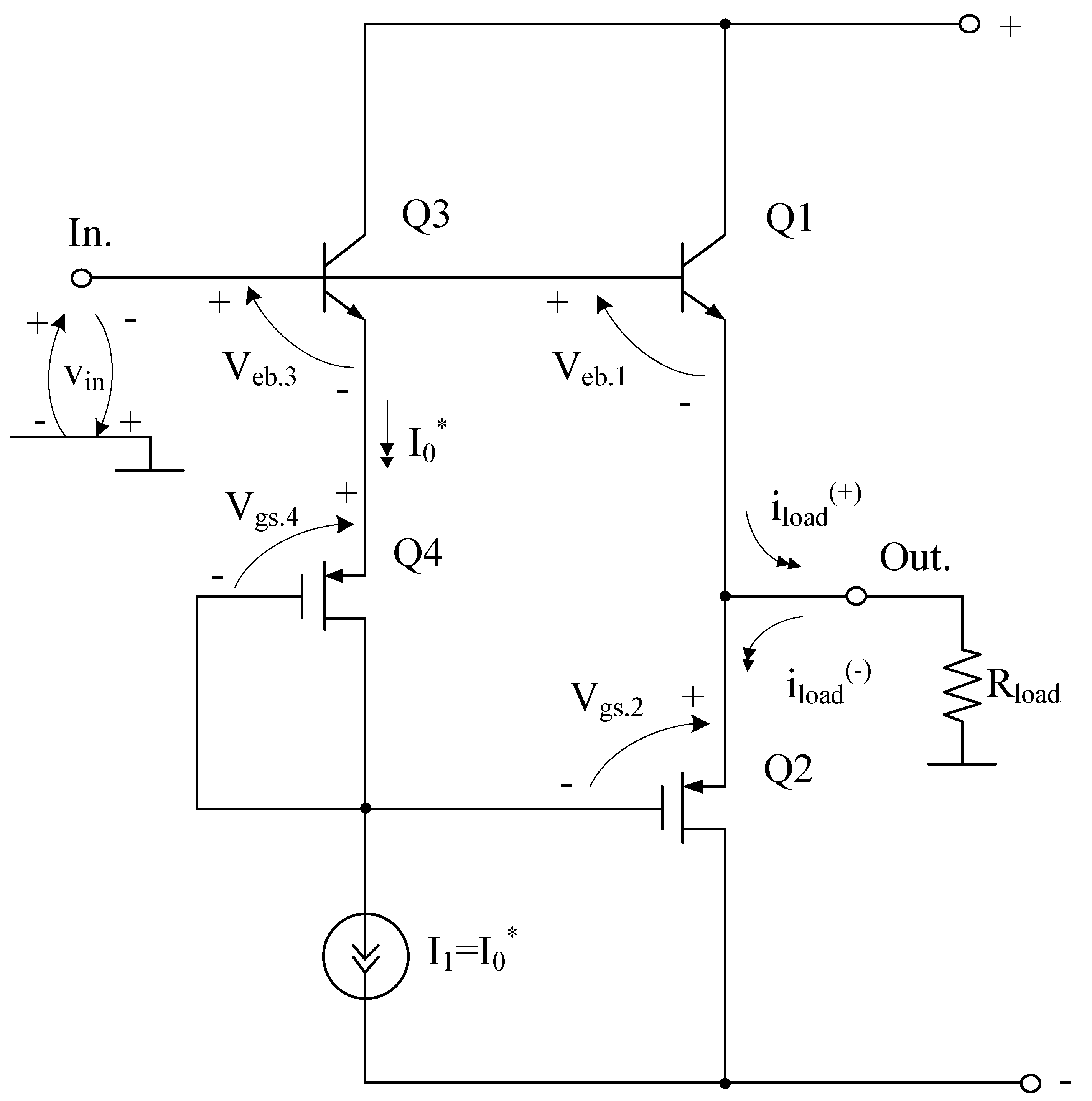
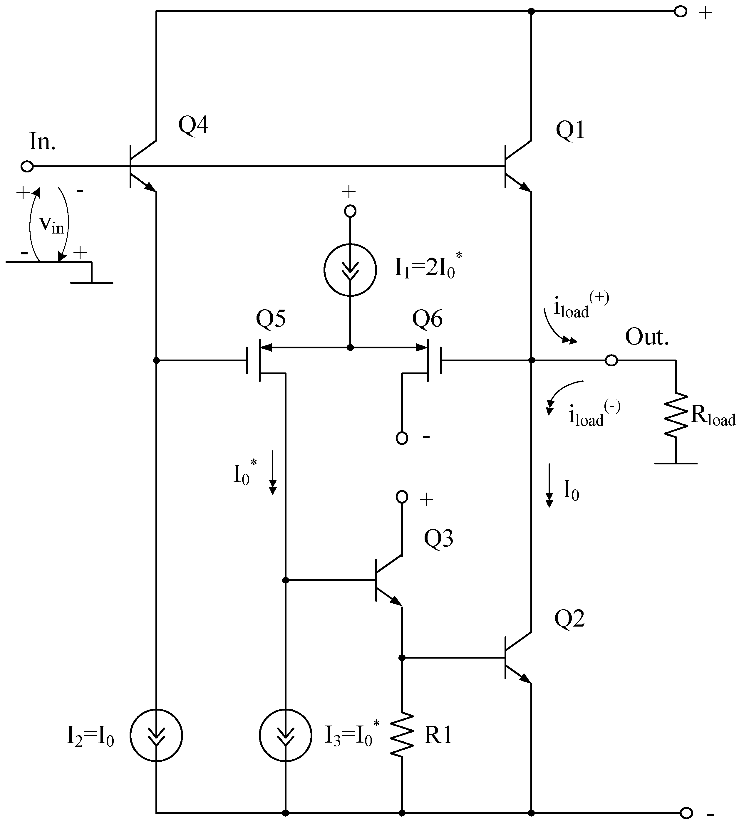
The feature of BA (Figure 5) is that the bipolar directions of the currents in the Rload are here formed by n-p-n transistors Q1, Q2, Q3 and depend on the current I0. Other elements of the BA circuit provide control of the state of transistors Q2 and Q3, and when Q1 goes into cutoff (at negative vin), they control transistors Q2 and Q3, which create negative current in the load. Adjustment of the BA circuit is provided by selection of resistances of resistors R1÷R2 and currents I1=I2.
Figure 5.
SiGe buffer amplifier: modification №2.
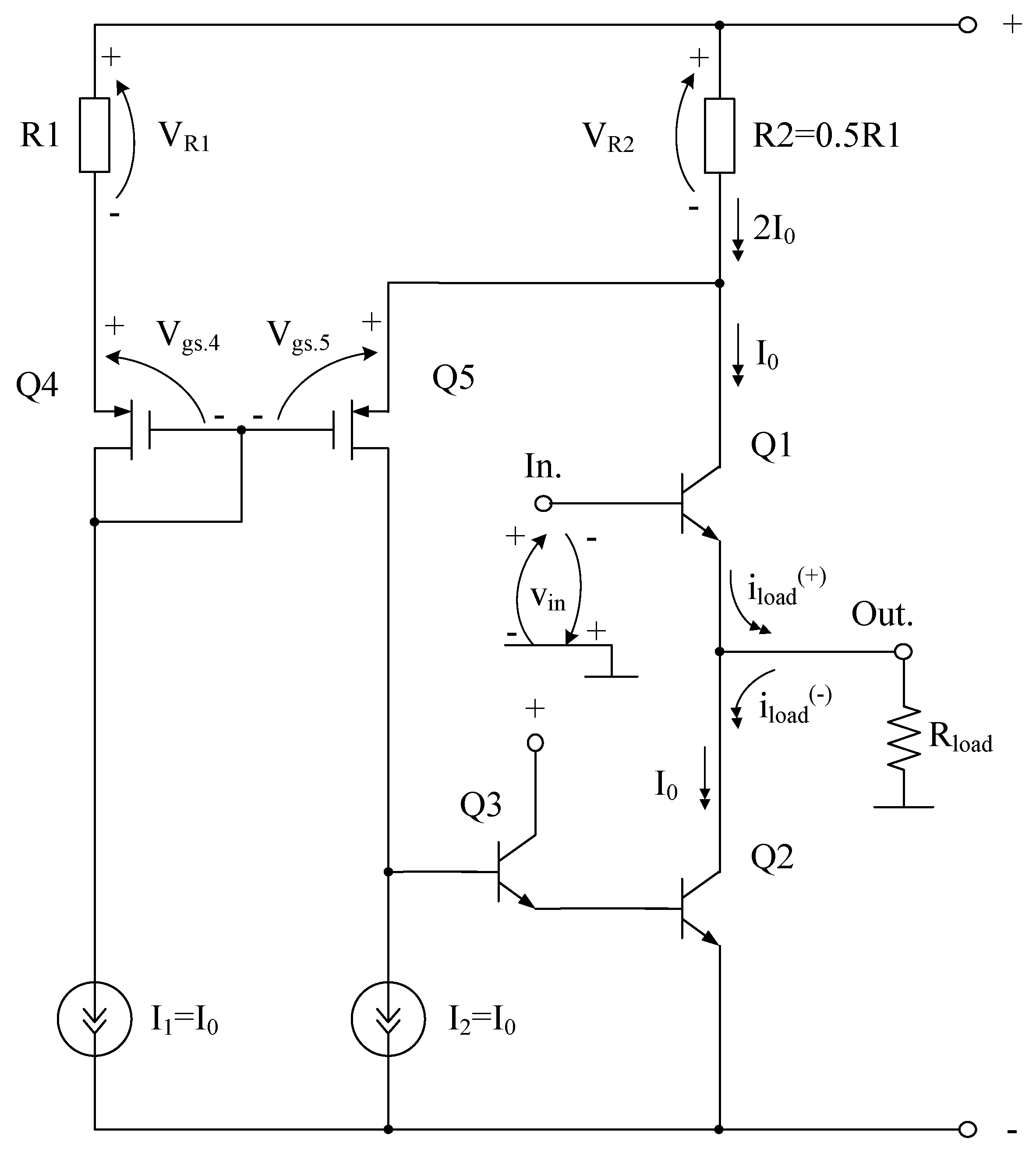
In this case and are determined by the formulas:
where – base current gain coefficients of bipolar transistors Q1÷Q3, – maximum possible value of SS (Figure 3) output current with positive vin, – source current I1.
Figure 6 shows the static mode of BA Figure 5 in Cadance simulation software at I4=I5=200 µA, resistors R2=500 Ω and R0=250 Ω, supply voltages ±3 V.
Figure 6.
Static mode of SiGe BA Fig.5 (modification №2) at t=27 oC.
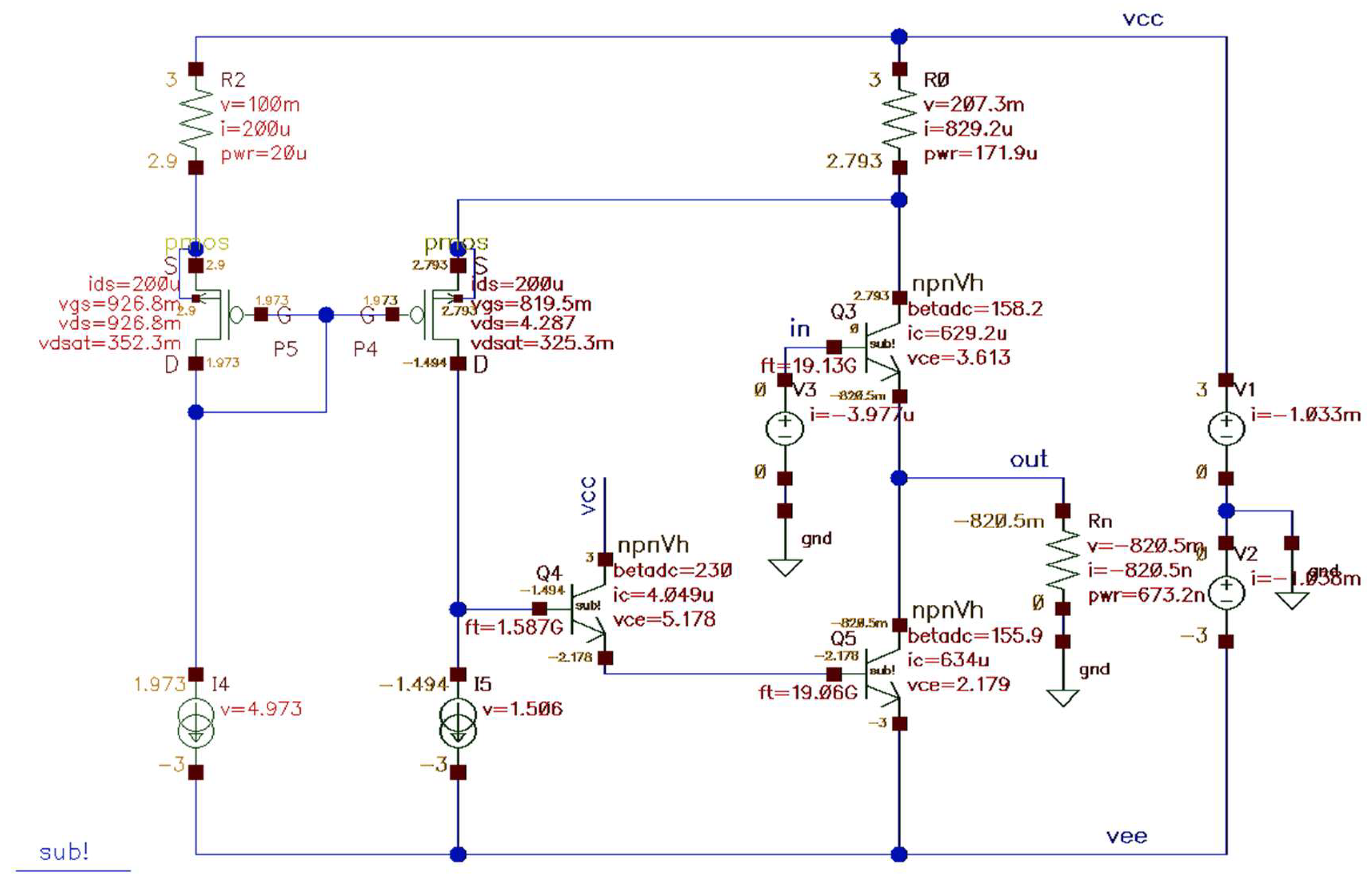
Figure 7.
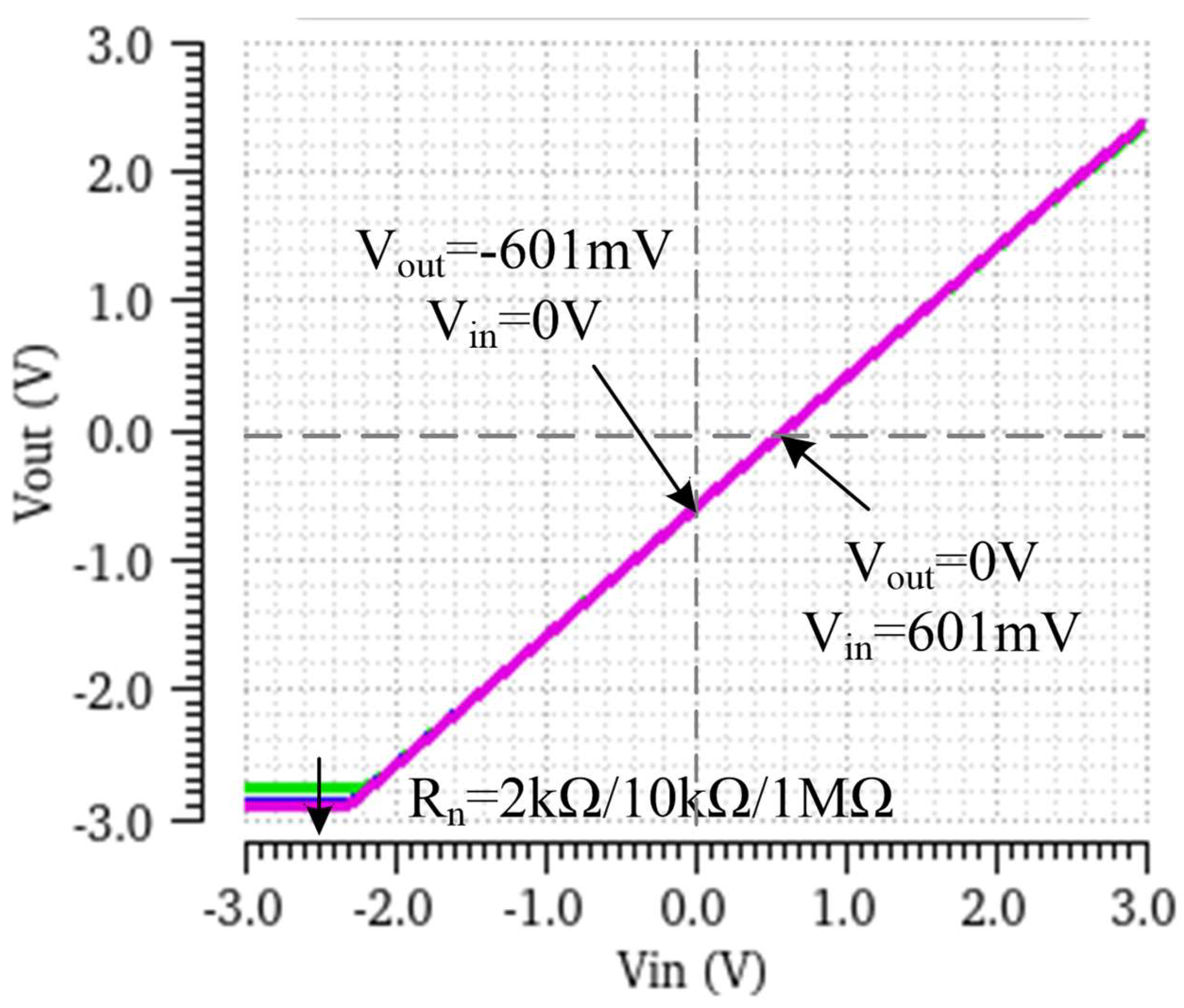
Amplitude characteristic of SiGe BA in Figure 6 at Rload=2 kΩ, 10 kΩ, t=27 oC.
Figure 7.
Amplitude characteristic of SiGe BA in Figure 6 at Rload=2 kΩ, 10 kΩ, t=27 oC.
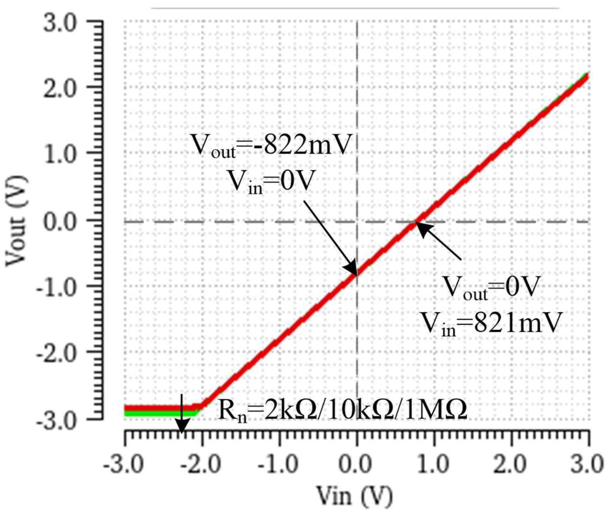
Figure 8 shows the static mode of BA Figure 5 in Cadance simulation software at t=250 oC, I4=I5=200 µA, resistors R2=500 Ω and R0=250 Ω, supply voltages ±3 V.
Figure 8.
Static mode of SiGe BA Fig.5 (modification №2) at t=250 oC.
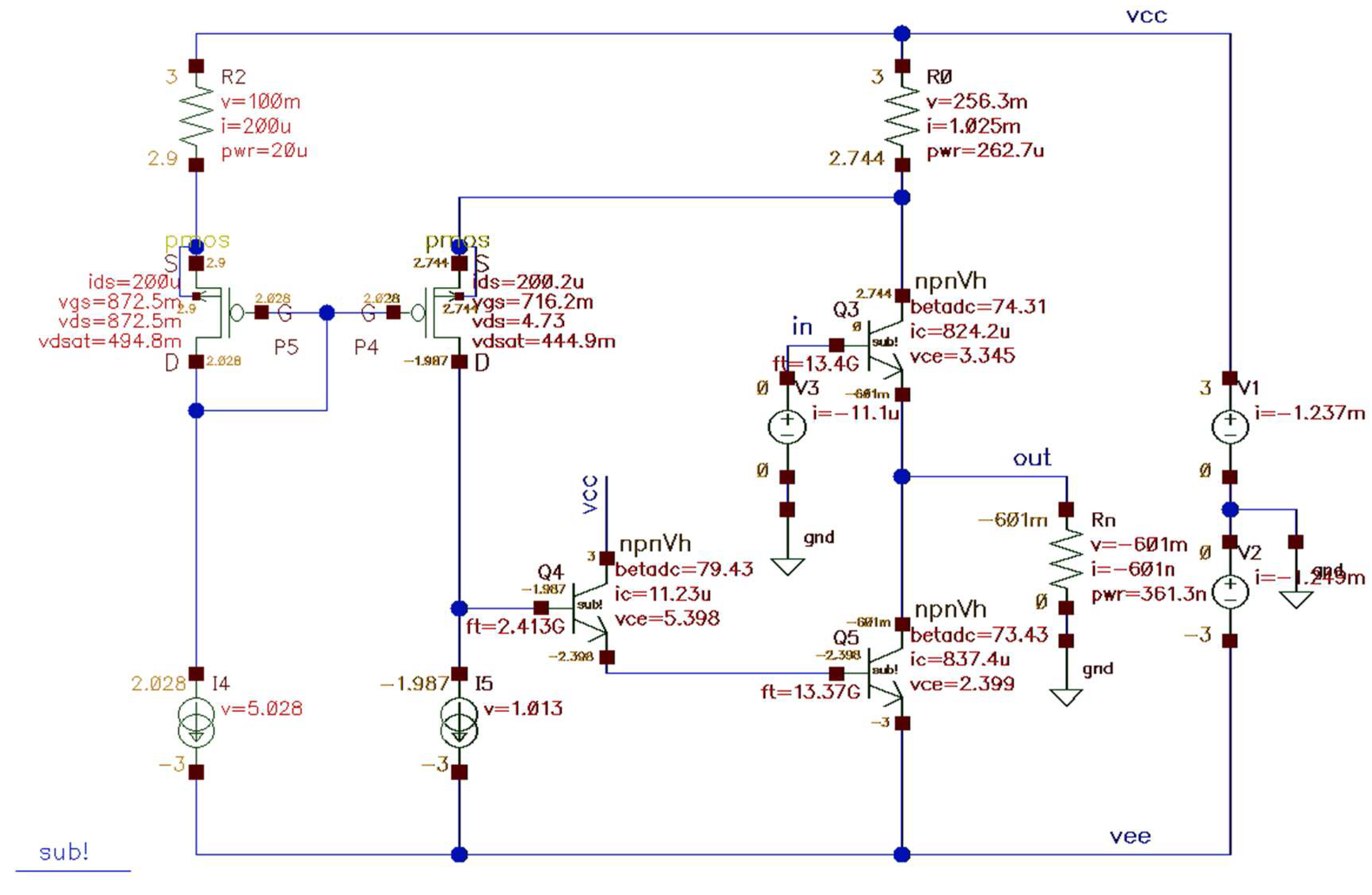
Figure 9.
Amplitude characteristic of SiGe BA in Figure 8 at Rload=2 kΩ, 10 kΩ, 1 MΩ, t=250 oC.
Figure 9.
Amplitude characteristic of SiGe BA in Figure 8 at Rload=2 kΩ, 10 kΩ, 1 MΩ, t=250 oC.
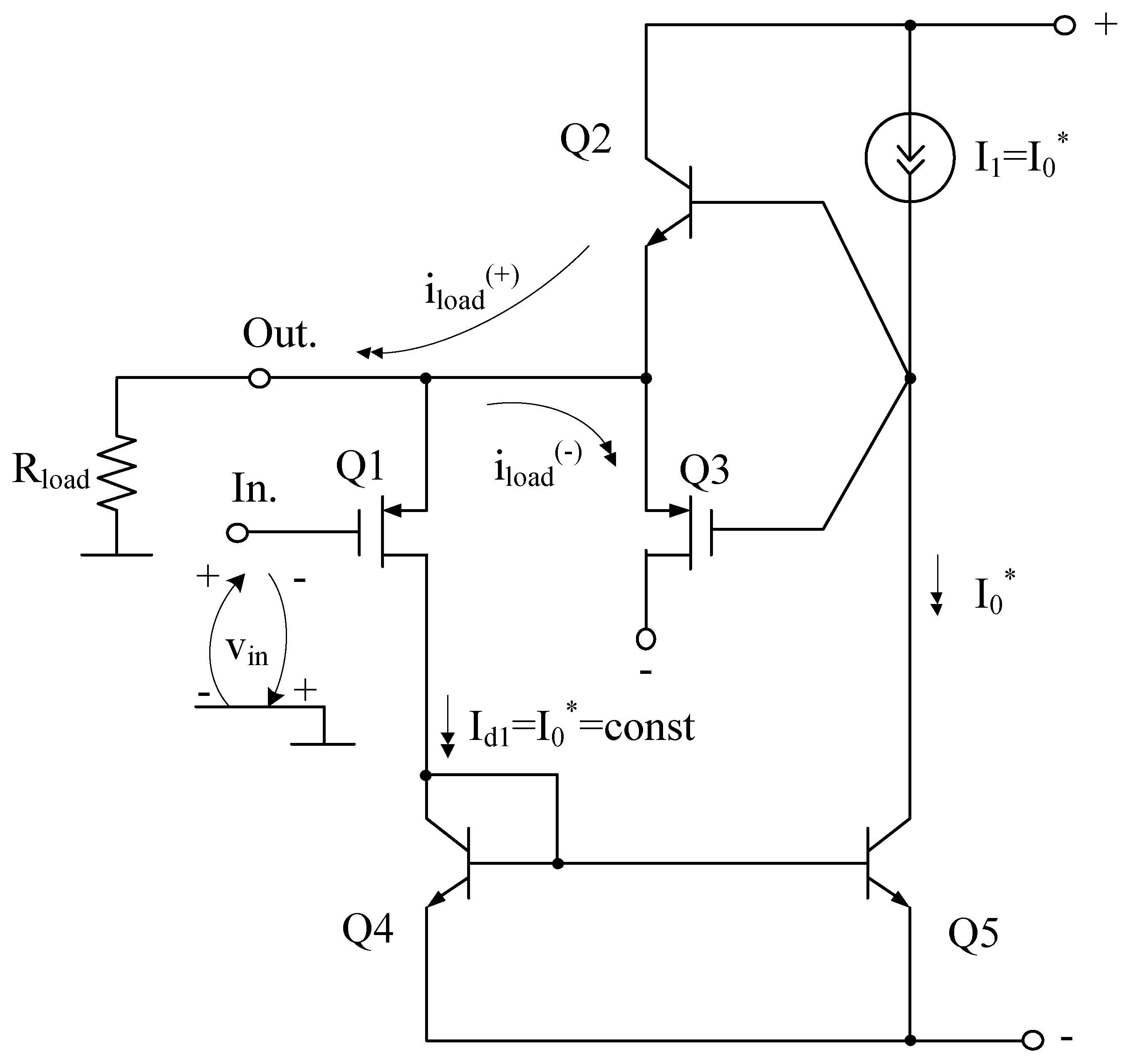
In circuit BA in Figure 10, the bipolar current directions in the Rload are formed by n-p-n transistors Q1, Q2, Q3. Other elements of the BA circuit provide state monitoring of transistor Q1 and, when Q1 goes into cutoff (at negative vin), control transistors Q2 and Q3, which create a negative current in the load. Setting of the BA circuit is provided by selection of resistors R1÷R3 and reference currents I1÷I4.
Figure 10.
SiGe buffer amplifier: modification №3.
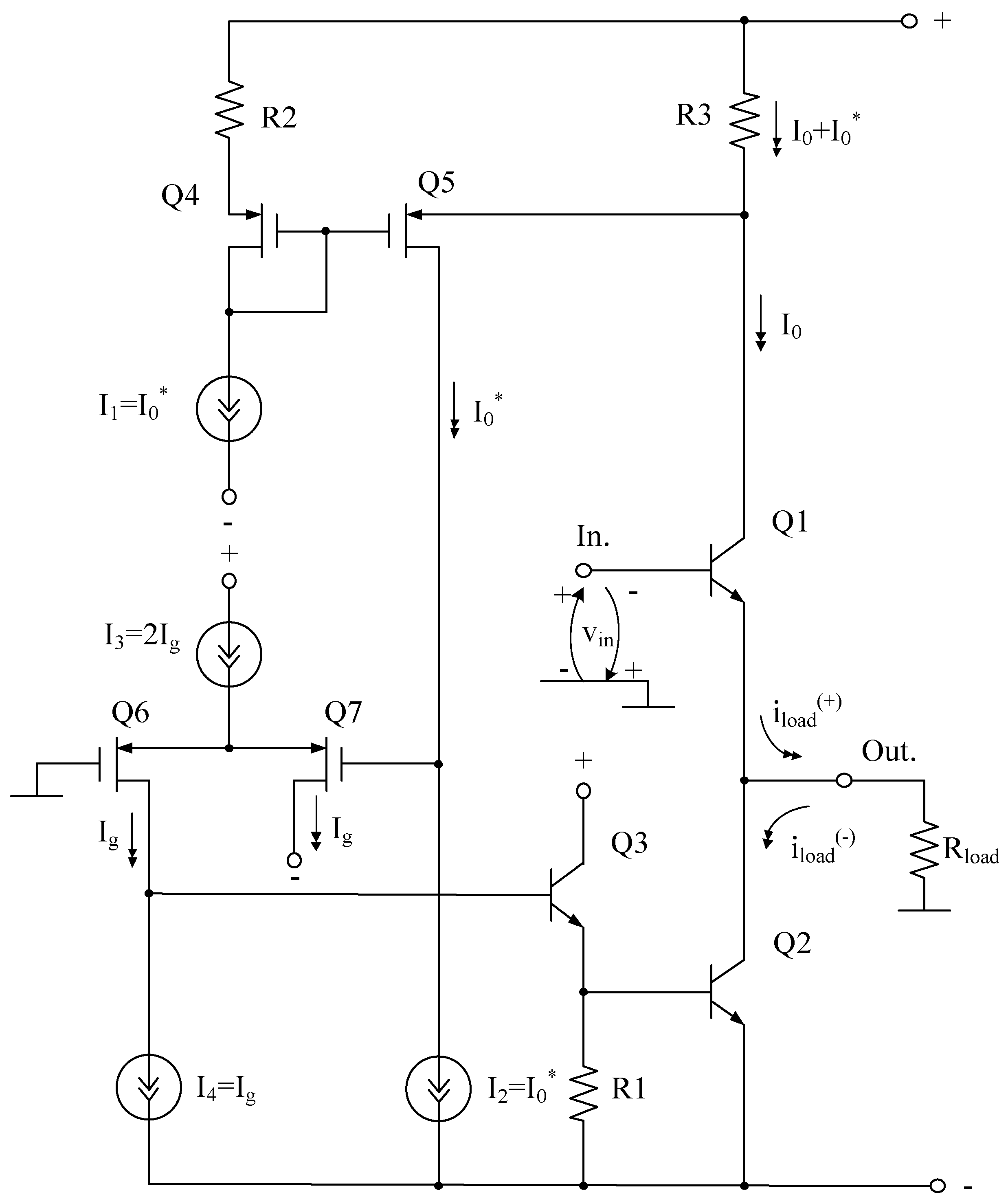
In this case and are determined by the formulas:
where – base current gain coefficients of bipolar transistors Q1÷Q3, – maximum possible value of SS (Figure 3) output current with positive vin, – current, seted by the source I3 (I3=2Ig).
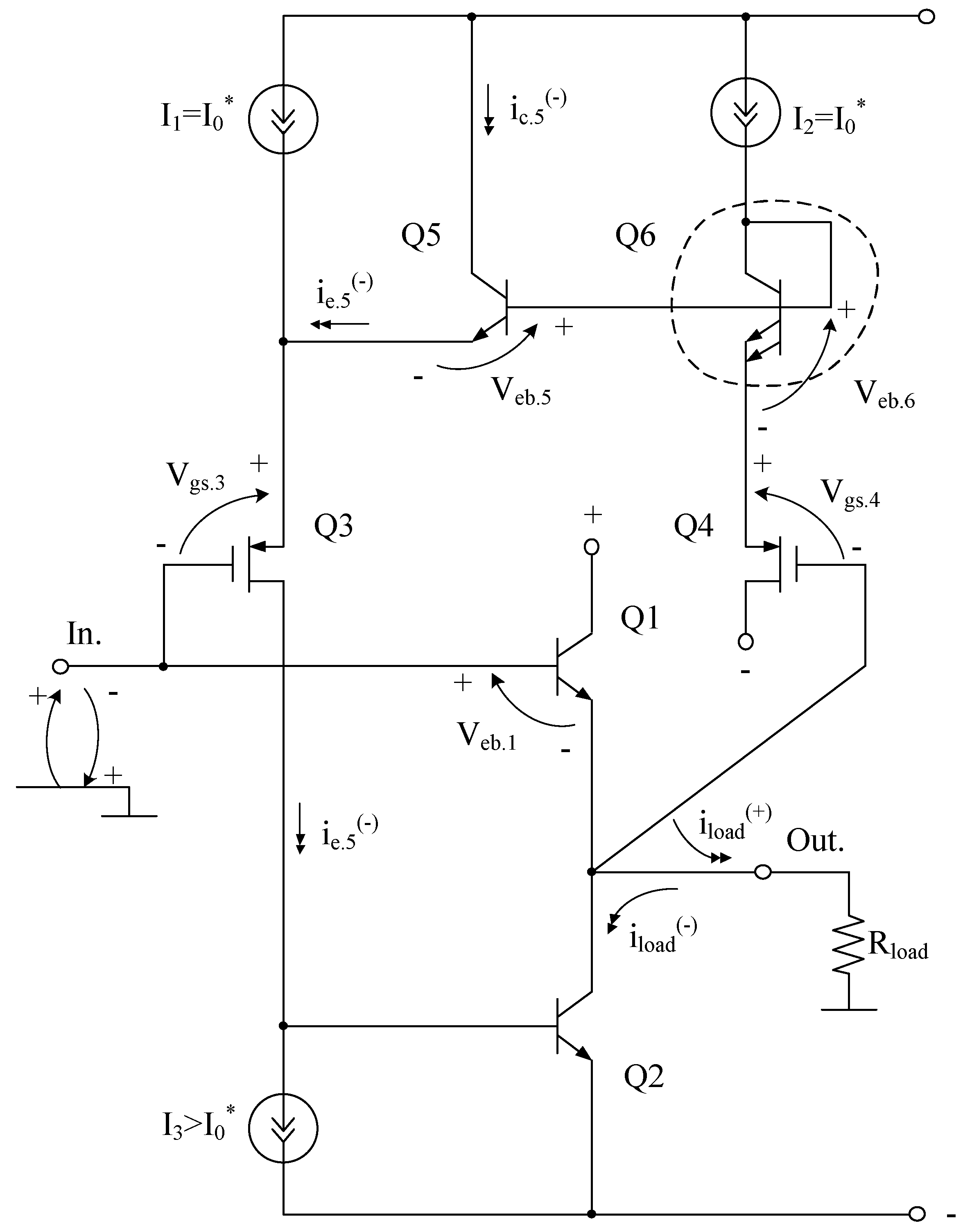
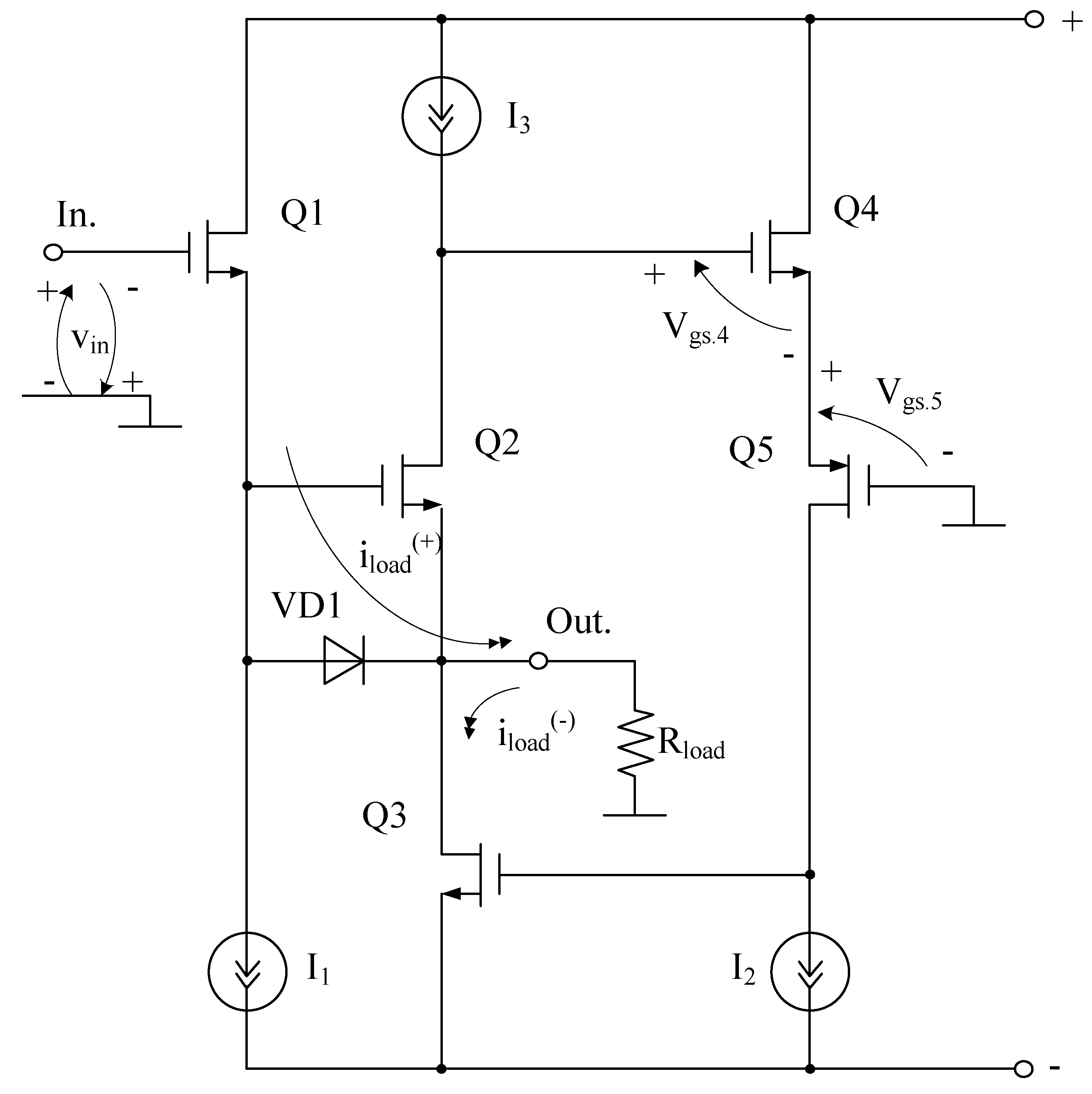
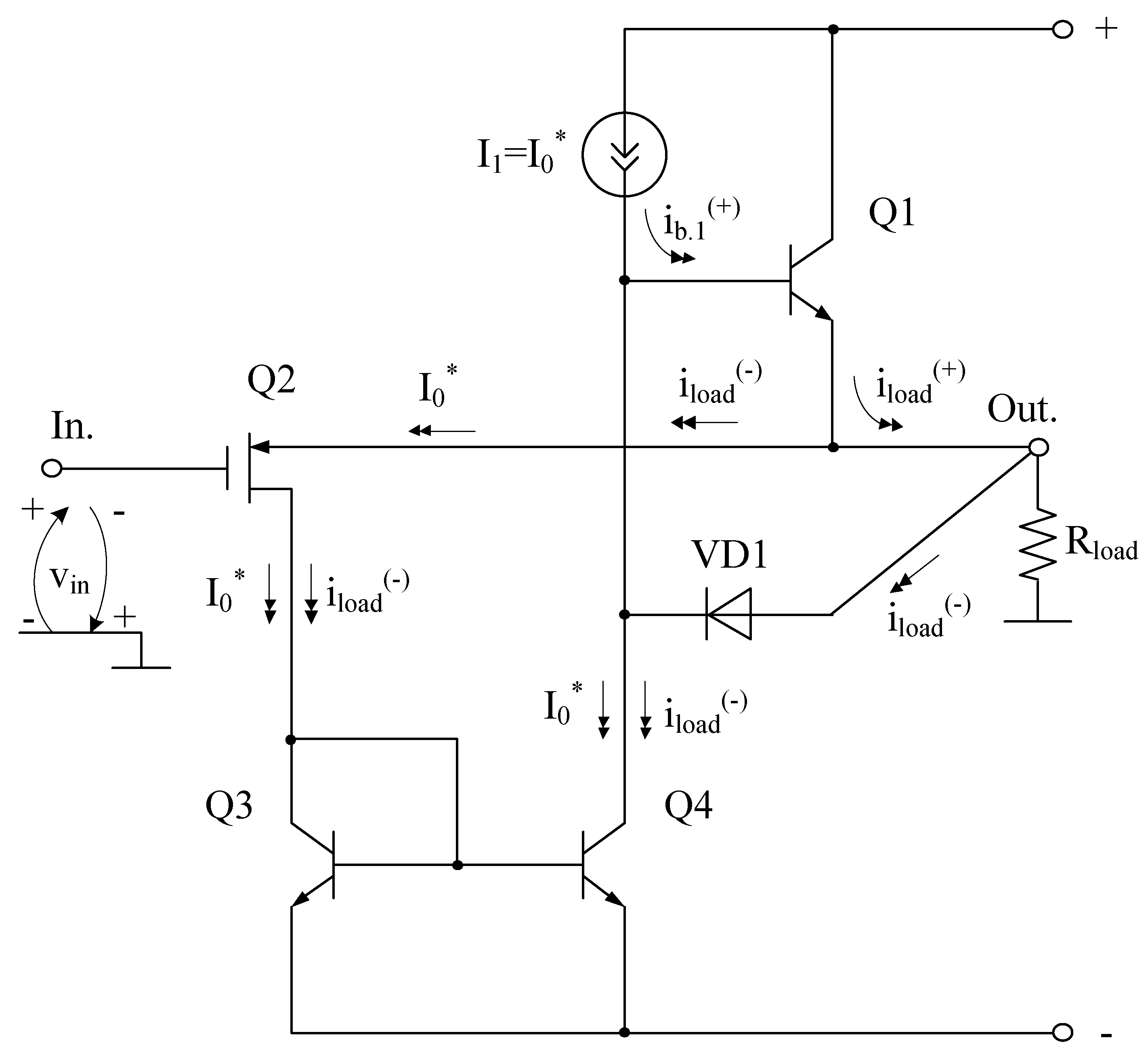
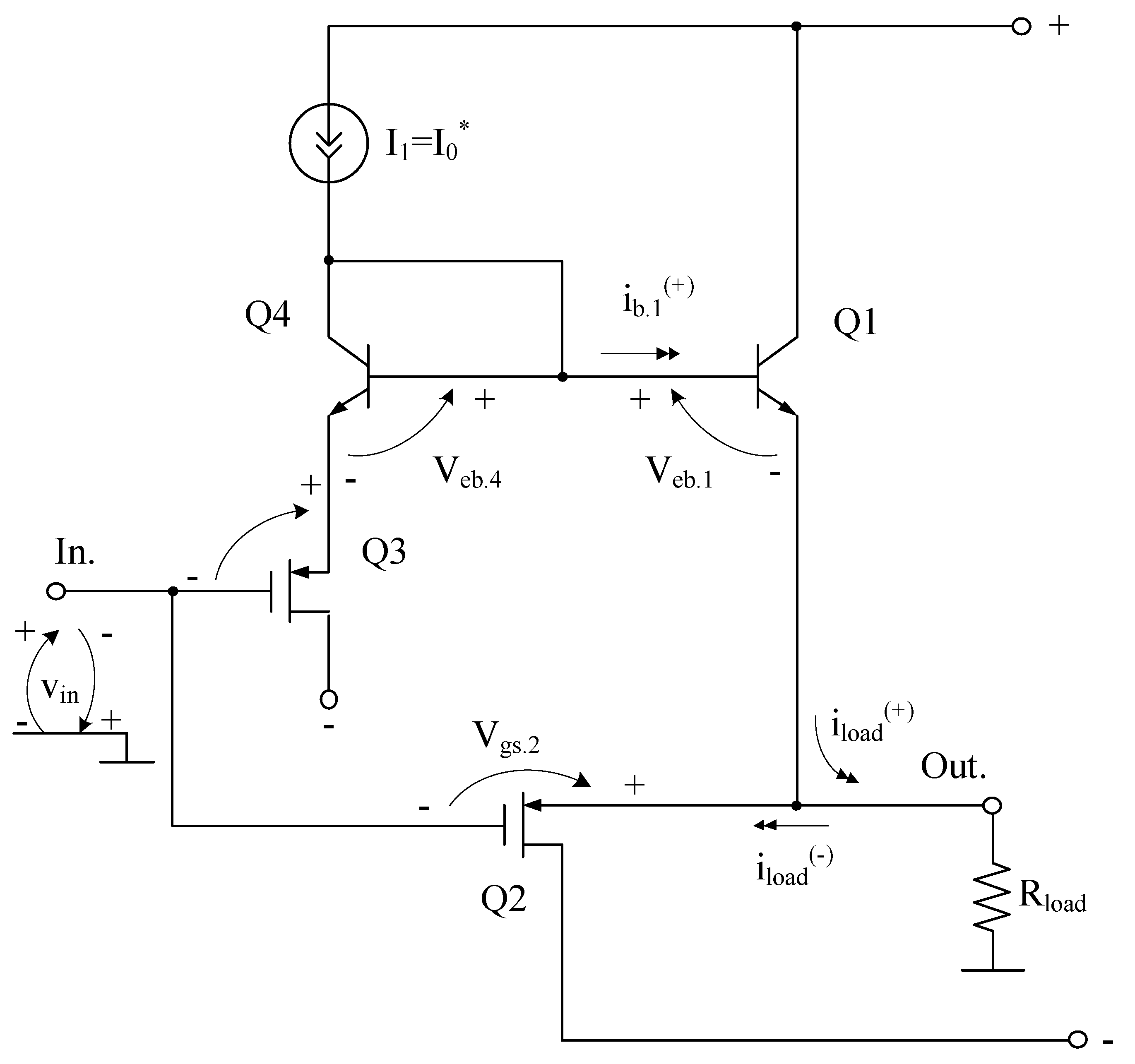
In the BA circuit of Figure 11, the p-n junction of VD1 limits the voltage drop across resistor R1 when the BA input voltages are positive and the big currents in load. Transistors Q3, Q4, and reference current source I1 set the static mode of Q5 and Q6. The BA circuit setting is provided by selection of resistors R1÷R2 and currents I1=I2.
Figure 11.
SiGe buffer amplifier: modification №4.
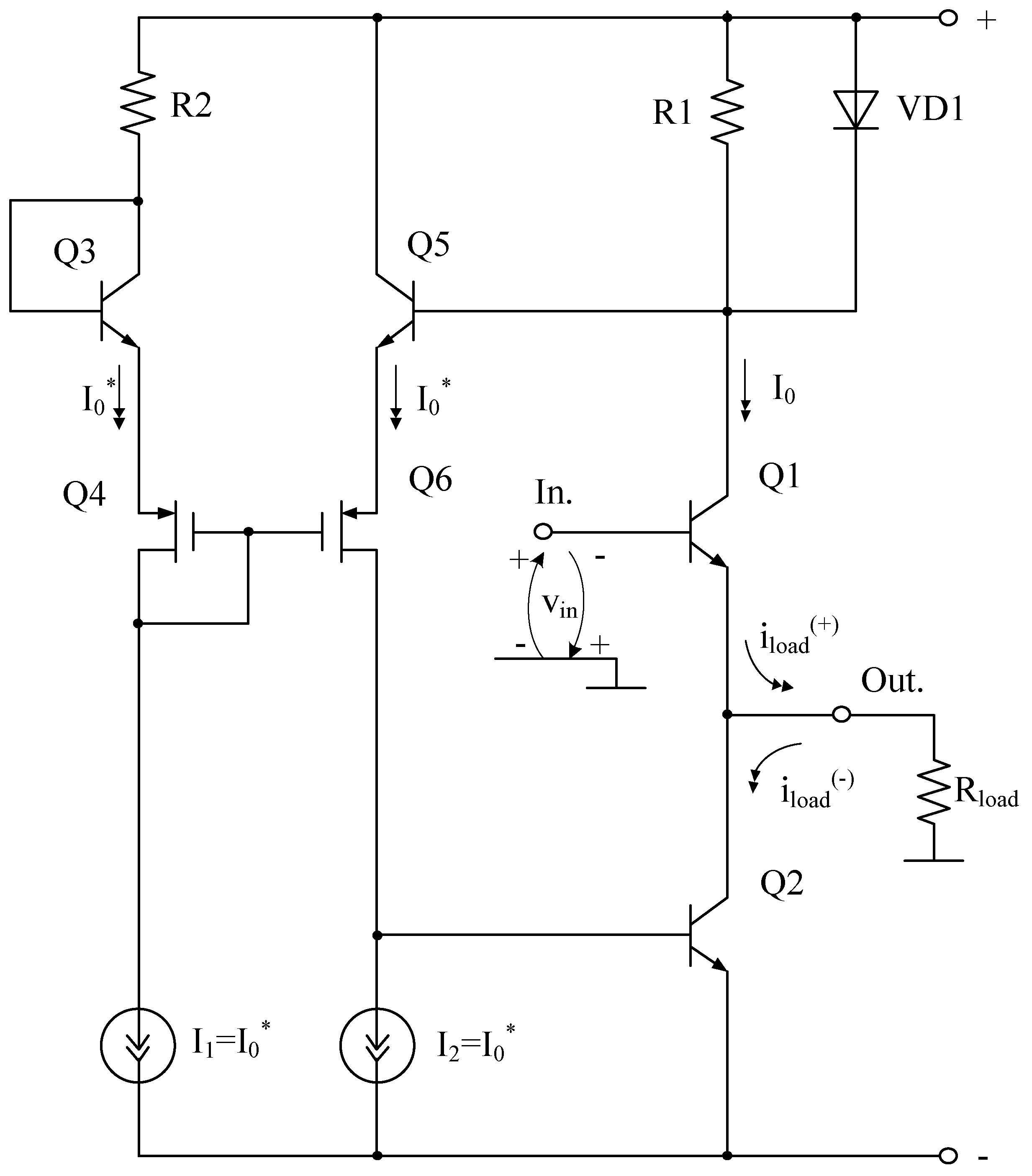
In this case and are determined by the formulas:
where , – base current gain coefficients of bipolar transistors Q1÷Q2, – maximum possible value of SS (Figure 3) output current with positive vin,– voltage drop across the resistor R1, – emitter junction resistance Q5, s6 – drain-gate transconductance Q6.
The peculiarity of BA (Figure 12) is that the bipolar directions of the currents in the Rload load are here formed by the n-p-n transistors Q1, Q2. Other elements of the BA circuit provide state control of the transistor Q1, and when Q1 goes into cutoff (at negative vin), control transistor Q2. The BA circuit is adjusted by selecting the currents 2I1=I2 and I3.
Figure 12.
SiGe buffer amplifier: modification №5.
In this case and are determined by the formulas:
where – maximum possible value of SS (Figure 3) output current with positive vin; , – base current gain coefficients of bipolar transistors Q1÷Q2, – two-terminal device current I1 .
In circuit BA in Figure 13, the static mode setting of the transistors is provided by selecting the reference current sources I1, I2, and I3.
Figure 13.
SiGe buffer amplifier: modification №6.
Here, the values of the maximum output currents and are determined by the formulas:
where – maximum possible value of SS (Figure 3) output current with positive vin; , – base current gain coefficients of bipolar transistors Q1÷Q2, . In this case .
The positive current direction in the load Rload in BA (Figure 14) is determined by the base current gain of the transistor Q1 and the reference current source I1. Adjustment of the BA circuit is provided by selection of currents I1=I2 and resistance of resistor R1.
Figure 14.
SiGe buffer amplifier: modification №7.

Thus in the scheme of Figure 14 the currents and are determined by the formulas:
where , – base current gain coefficients of bipolar transistors Q1÷Q2, – two-terminal device current I1, – maximum amplitude of the input signal when negative vin, R1 – resistor resistance R1, s4 – the steepness of the drain-gate characteristic of the transistor Q4.
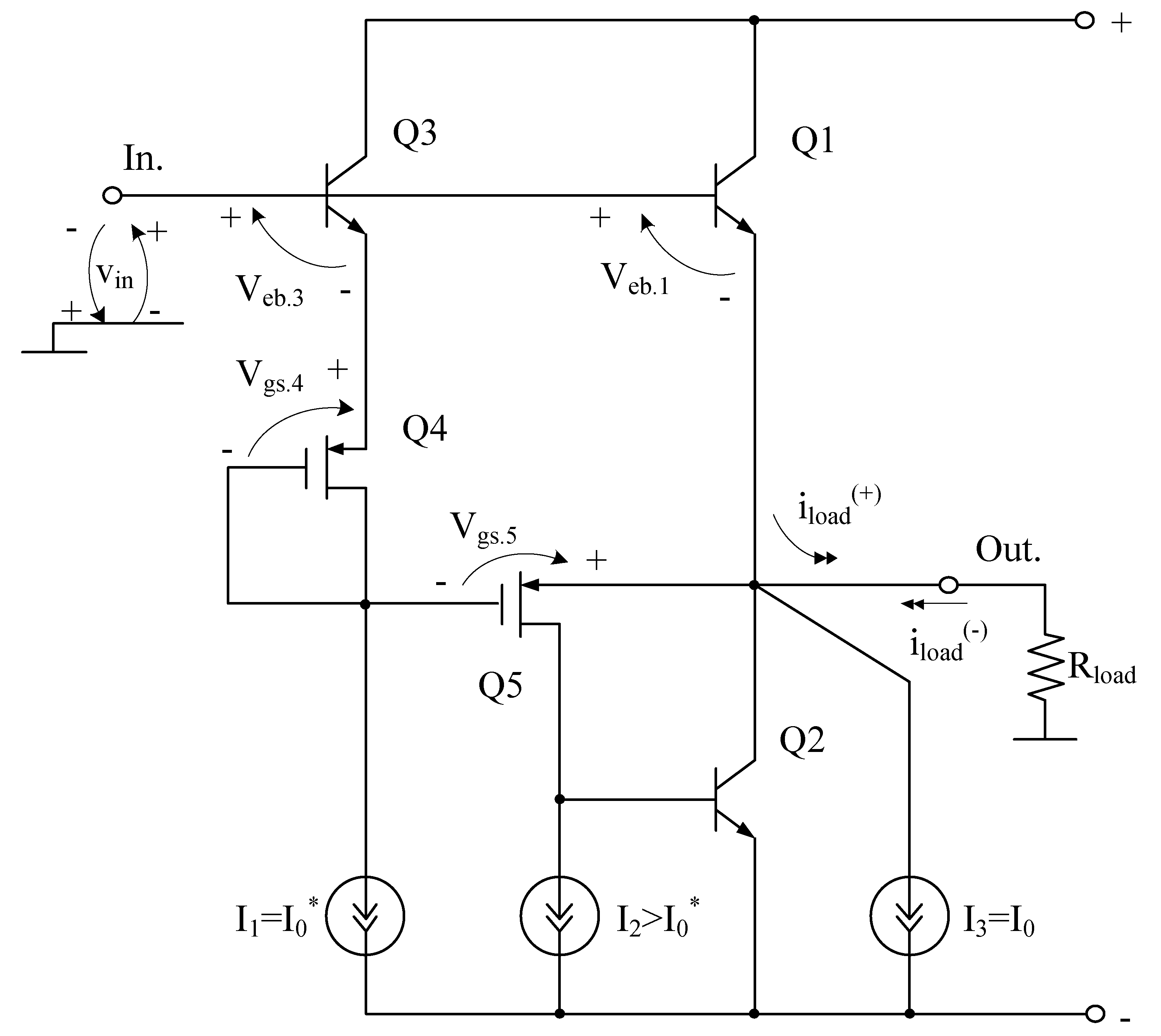
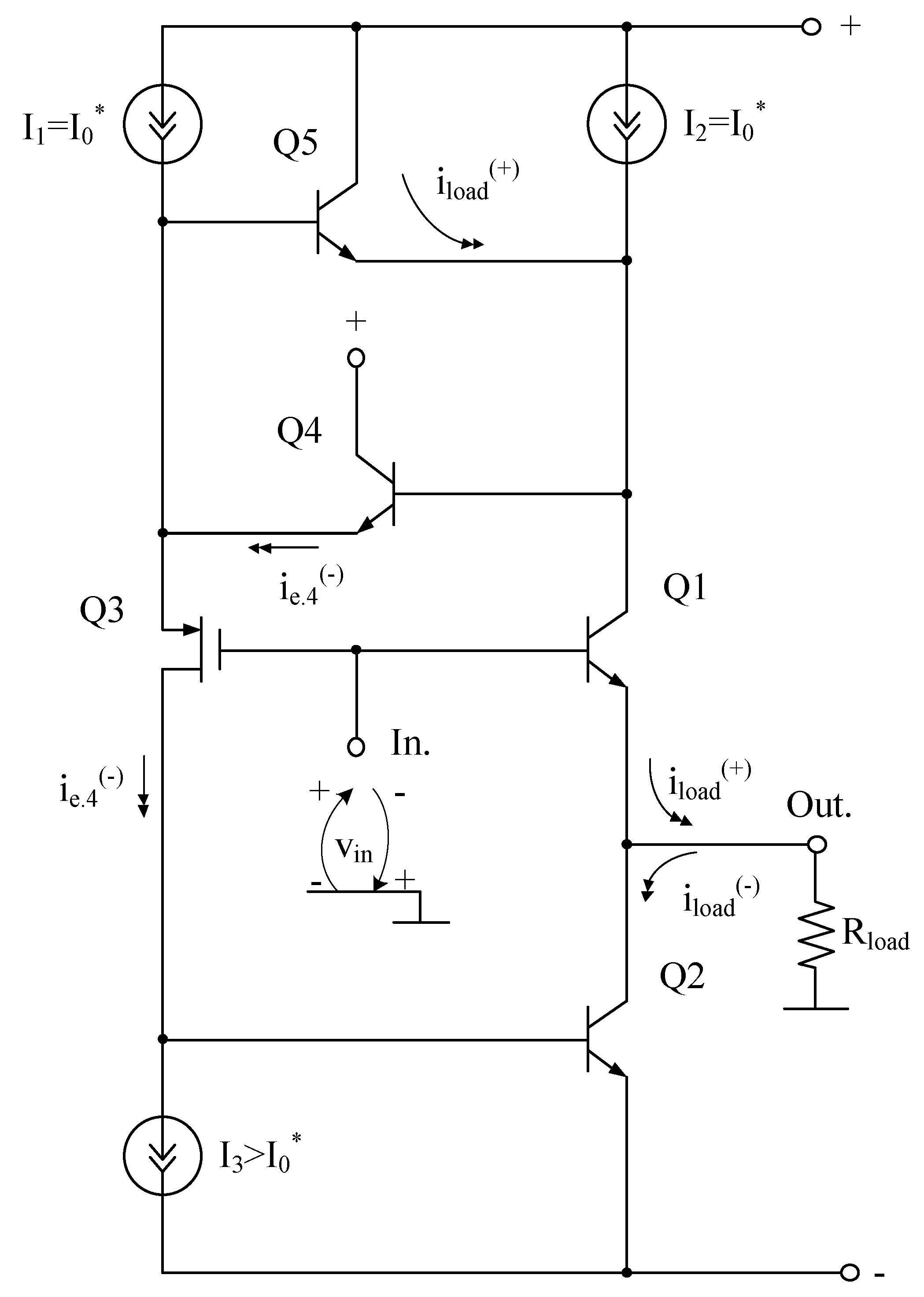
The peculiarity of BA in Figure 15 is that the bipolar directions of the currents in the Rload load here are determined by transistors Q1, Q2, Q5, the maximum possible value of the output current of the intermediate stage (Figure 3) at positive vin, and the source current I2. The BA circuit is configured by selecting the numerical values of I1=I2 and I3.
Figure 15.
SiGe buffer amplifier: modification №8.
In this case and are determined by the formulas:
where ,, – base current gain coefficients of bipolar transistors Q1, Q2, Q5; – maximum possible value of SS (Figure 3) output current with positive vin;– two-terminal device current I1=I2.
In circuit BA in Figure 16, the positive currents in the load Rload are generated by the n-p-n transistor Q1 and the negative currents by the field-effect transistor Q2. The circuit is adjusted by selecting the current I1.
Figure 16.
SiGe buffer amplifier: modification №9.
In this case, the maximum currents and are determined by the formulas:
where – base current gain coefficient of bipolar transistor Q1, – maximum possible value of SS (Figure 3) output current with positive vin, – maximum transistor current Q2.
The BA circuit (Figure 17) differs from the BA circuit Figure 16 by the use of bipolar transistor Q2, which together with field-effect transistor Q5 provides negative currents in the load Rload. Adjustment of the BA circuit is provided by selection of currents I1, I2 and I3.
Figure 17.
SiGe buffer amplifier: modification №10.
In the circuit of Figure 17, the maximum currents are and are determined by the formulas:
where – base current gain coefficient of bipolar transistor Q1, – maximum possible value of SS (Figure 3) output current with positive vin, – maximum collector current of the transistor Q2.
BA Figure 18 is realized on complementary field-effect transistors Q1, Q2 and Q3, Q4. Moreover, Q1 and Q3 and the reference current source I1 set the static mode of transistors Q2, Q4. The adjustment of the BA circuit is provided by selecting the current I1, and also by changing the channel widths of the transistors.
Figure 18.
SiGe buffer amplifier: modification №11.
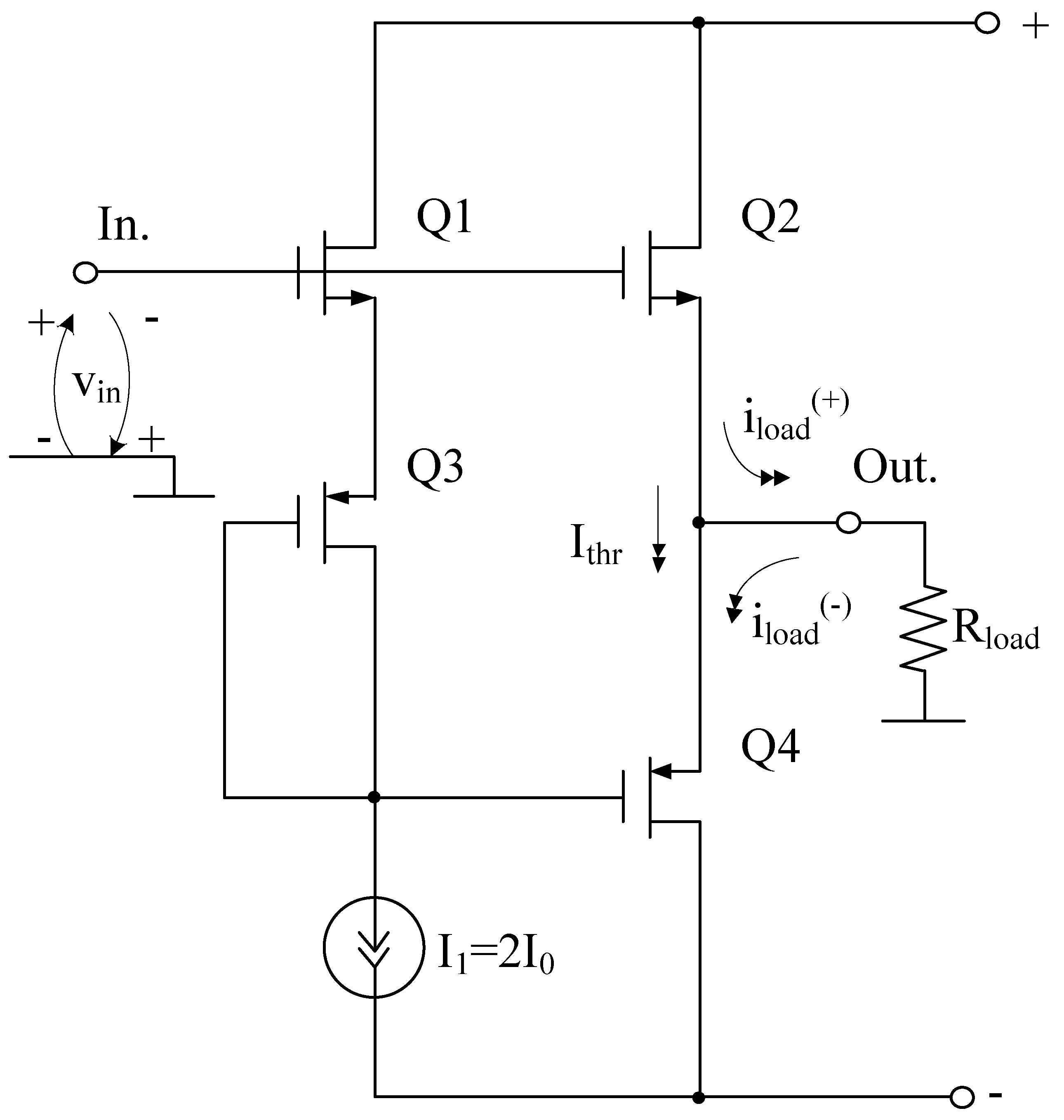
In this case and are determined by the formulas:
where – maximum transistor drain current Q2, – maximum transistor drain current Q4.
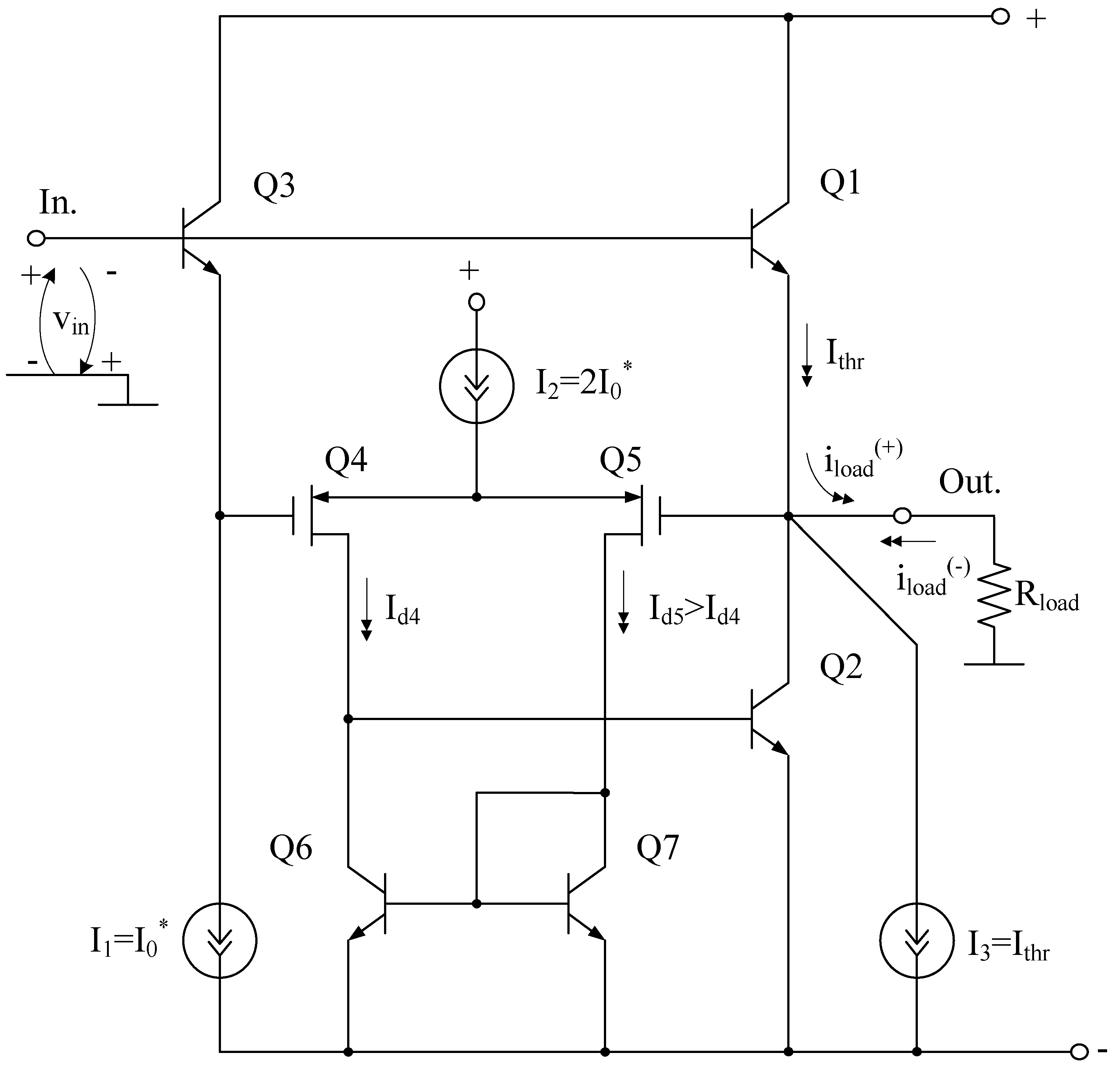
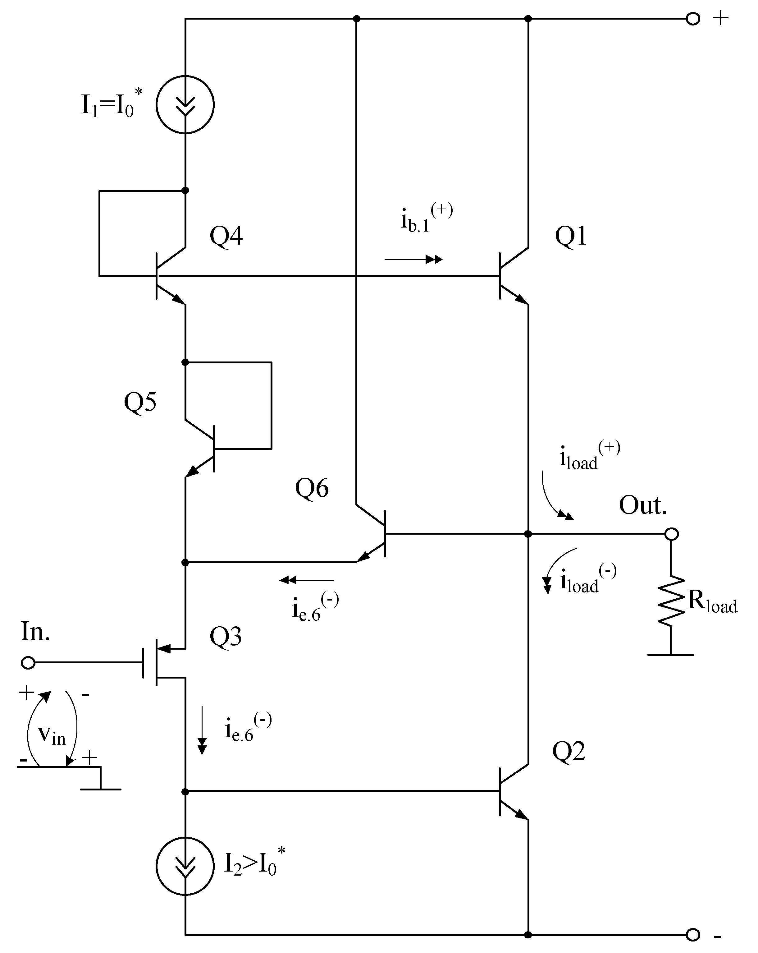
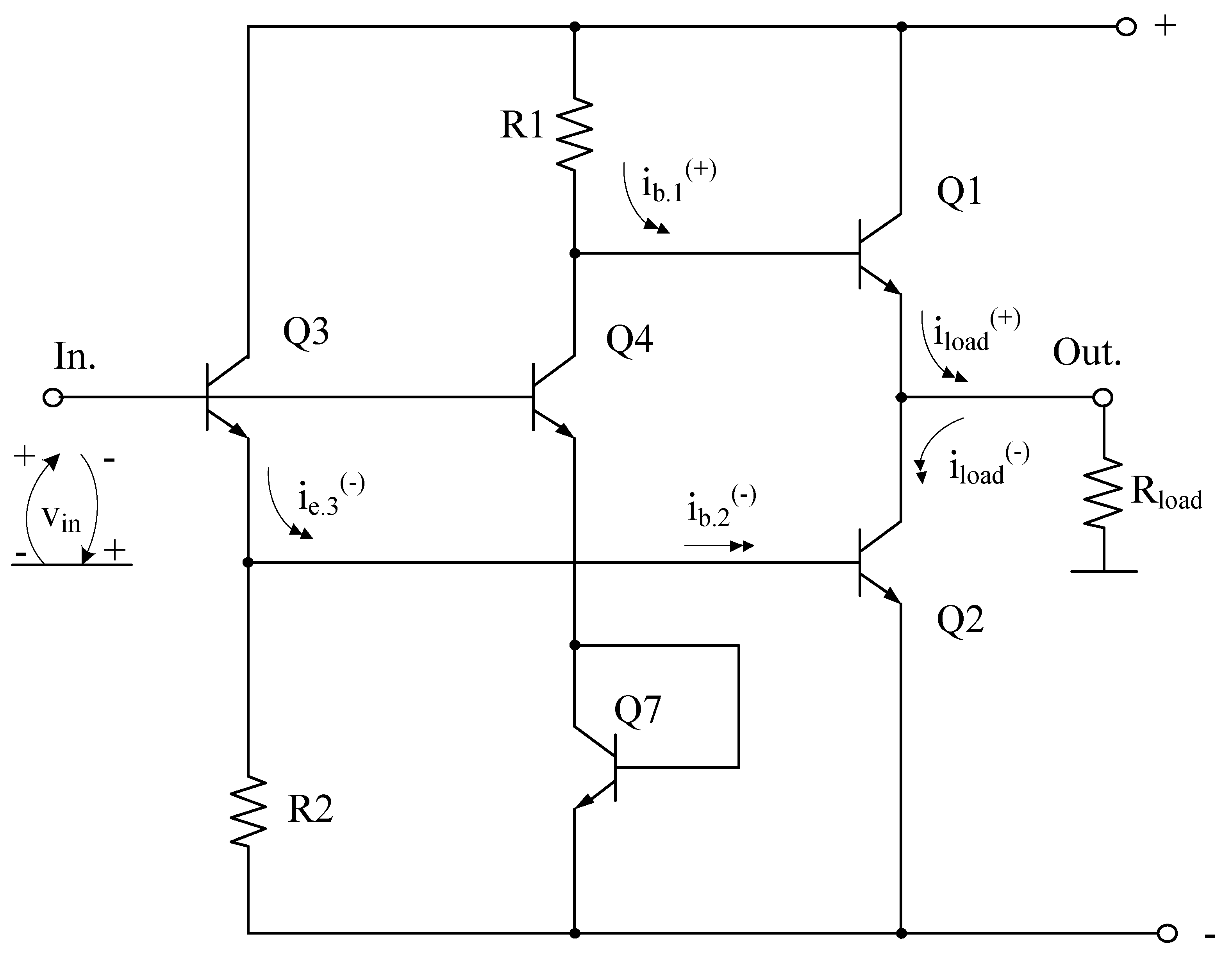
In the circuit of Figure 19, control of the state of transistor Q1 by the emitter-base voltage is provided by a differential stage on transistors Q5 and Q6, which compare the emitter-base voltages of transistors Q1 and Q4 and, when Q1 is latched, controls transistors Q3, Q2. This generates a negative current direction in the load. Adjustment of the BA circuit is provided by selection of currents I1=2I2, I3 and resistance of resistor R1.
Figure 19.
SiGe buffer amplifier: modification №12.
In circuit BA Figure 19 the maximum currents in the load and are determined by the formulas:
where , , – base current gain coefficients of bipolar transistors Q1÷Q3, – maximum possible value of SS (Figure 3) output current with positive vin, .
The BA circuit in Figure 20 is realized on complementary field-effect transistors Q1÷Q4. Adjustment of the BA circuit is provided by selection of currents I1, I2, I3.
Figure 20.
SiGe buffer amplifier: modification №13.
In this case and are determined by the formulas:
where – maximum transistor drain current Q1, – maximum transistor drain current Q3.
In circuit BA (Figure 21), the status of transistor Q1 is monitored by numerical values of its collector current, which is compared with the source current I1. At high positive currents in the load, the p-n junction of VD1 opens, through which iload(+)is shorted to the low impedance bias circuit source Vbias1. The BA circuit is set up by selecting currents I1, I2, and sources Vbias1, Vbias2.
Figure 21.
SiGe buffer amplifier: modification №14.
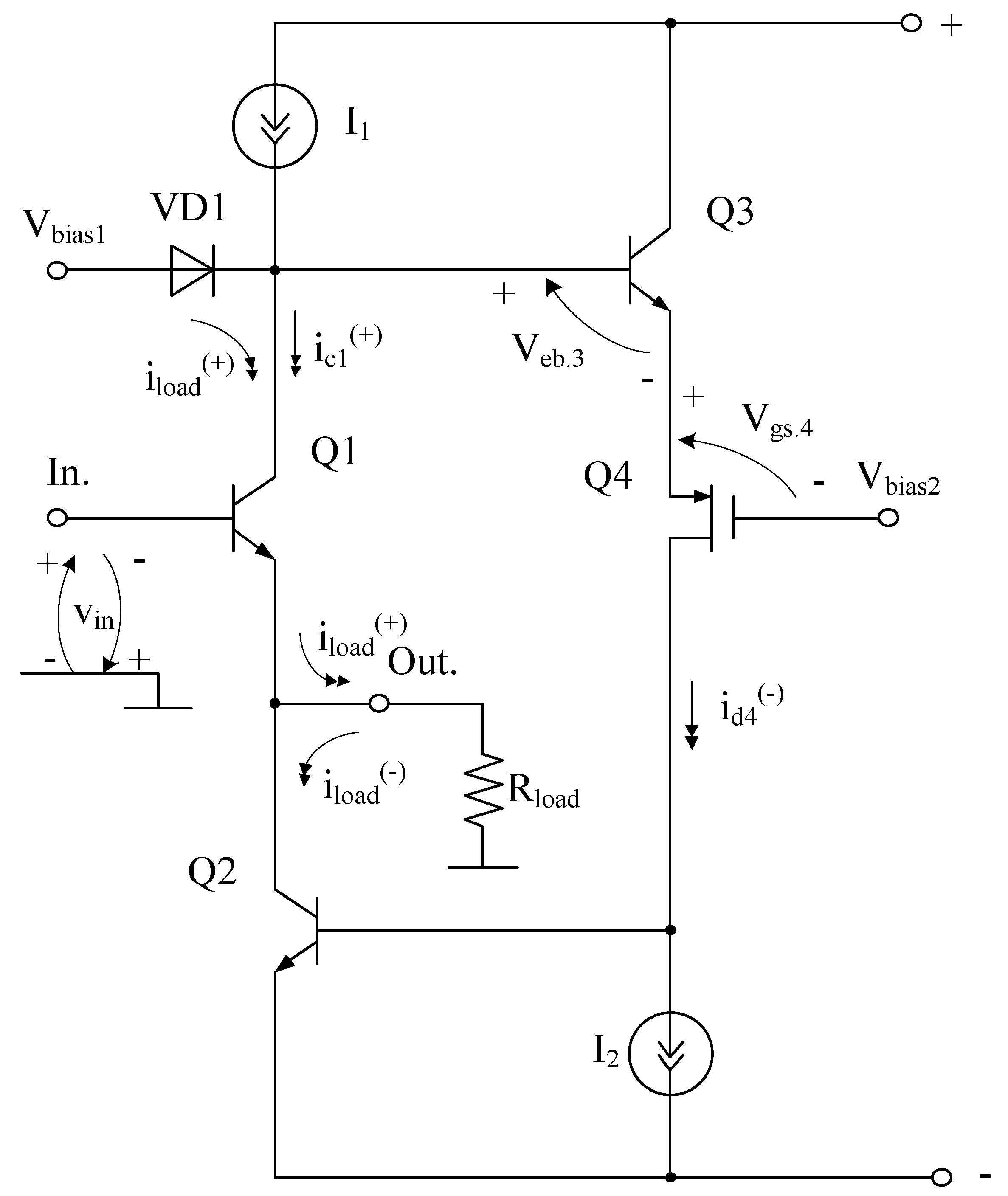
In this case, the currents and are determined by the formulas:
where ,, – base current gain coefficients of bipolar transistors Q1÷Q3, – maximum possible value of SS (Figure 3) output current with positive vin.
The circuit BA in Figure 22 has an increased input impedance due to the use of the field-effect transistor Q3. The BA setting is provided by selecting the currents I1, I2.
Figure 22.
SiGe buffer amplifier: modification №15.
In this case, the maximum currents and are determined by the formulas:
where – base current gain coefficient of bipolar transistor Q1, , – maximum collector current of the transistor Q2, .
BA (Figure 23) is realized on n-p-n bipolar transistor Q1 and field-effect transistors Q2, Q4. The BA circuit is tuned by selecting the current I1.
Figure 23.
SiGe buffer amplifier: modification №16.

In this case, the maximum currents in the load and are defined by the formulas:
where – current gain of the base of the bipolar transistor Q1, – maximum possible value of SS (Figure 3) output current with positive vin, – maximum transistor drain current Q4.
In the BA circuit (Figure 24), the current in the load in the positive direction is provided by the bipolar transistor Q2 and in the negative direction by the field-effect transistor Q3. The BA static mode is set by selecting the current I1.
Figure 24.
SiGe buffer amplifier: modification №17.
In this case, the maximum currents in the load and are determined by the formulas:
where – current gain of the base of the bipolar transistor Q2, , – maximum drain current of the field-effect transistor Q3.
The peculiarity of BA in Figure 25 is that the bipolar directions of the currents in the Rload are here determined by transistor Q1, bipolarized by I1 (at positive vin) and field-effect transistor Q2 (at negative vin). The static mode of the BA circuit is set by selecting the current .
Figure 25.
SiGe buffer amplifier: modification №18.
In this circuit the currents and are determined by the formulas:
where – current gain of the base of the bipolar transistor Q1, , – maximum drain current of the field-effect transistor Q2.
Figure 26 shows a generalized scheme BA, which can have several partial variants of construction, which is determined by the practical implementation of comparison schemes OA1, OA2. Setting BA to the limiting parameters is provided by the choice of OA1, OA2.
Figure 26.
SiGe buffer amplifier: modification №19.
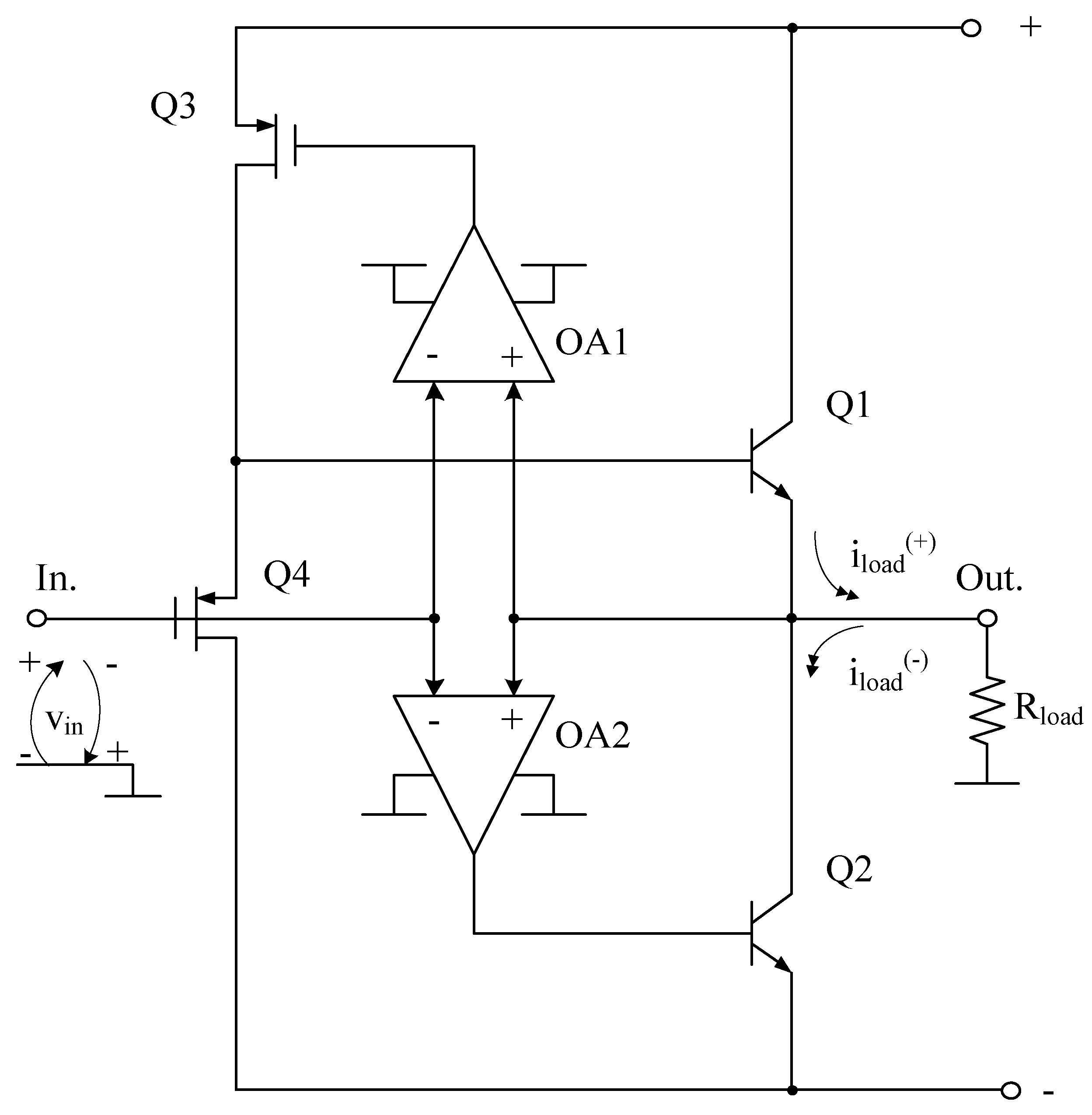
In this case, the currents and are determined by the formulas:
where – maximum collector current of the transistor Q1, – maximum collector current of the transistor Q2.
The peculiarity of the scheme BA in Figure 27 is that by selecting the channel width of transistor Q3 and the resistance of resistor R1, the numerical values of the through current of transistors Q1 and Q2 are set. The setting of the BA is ensured by selecting the current I1 and the resistance of resistor R1.
Figure 27.
SiGe buffer amplifier: modification №20.
In this case, the currents and are determined by the formulas:
where – current gain of the base of the bipolar transistor Q1, – maximum possible value of SS (Figure 3) output current with positive vin, – maximum drain current of the field-effect transistor Q2.
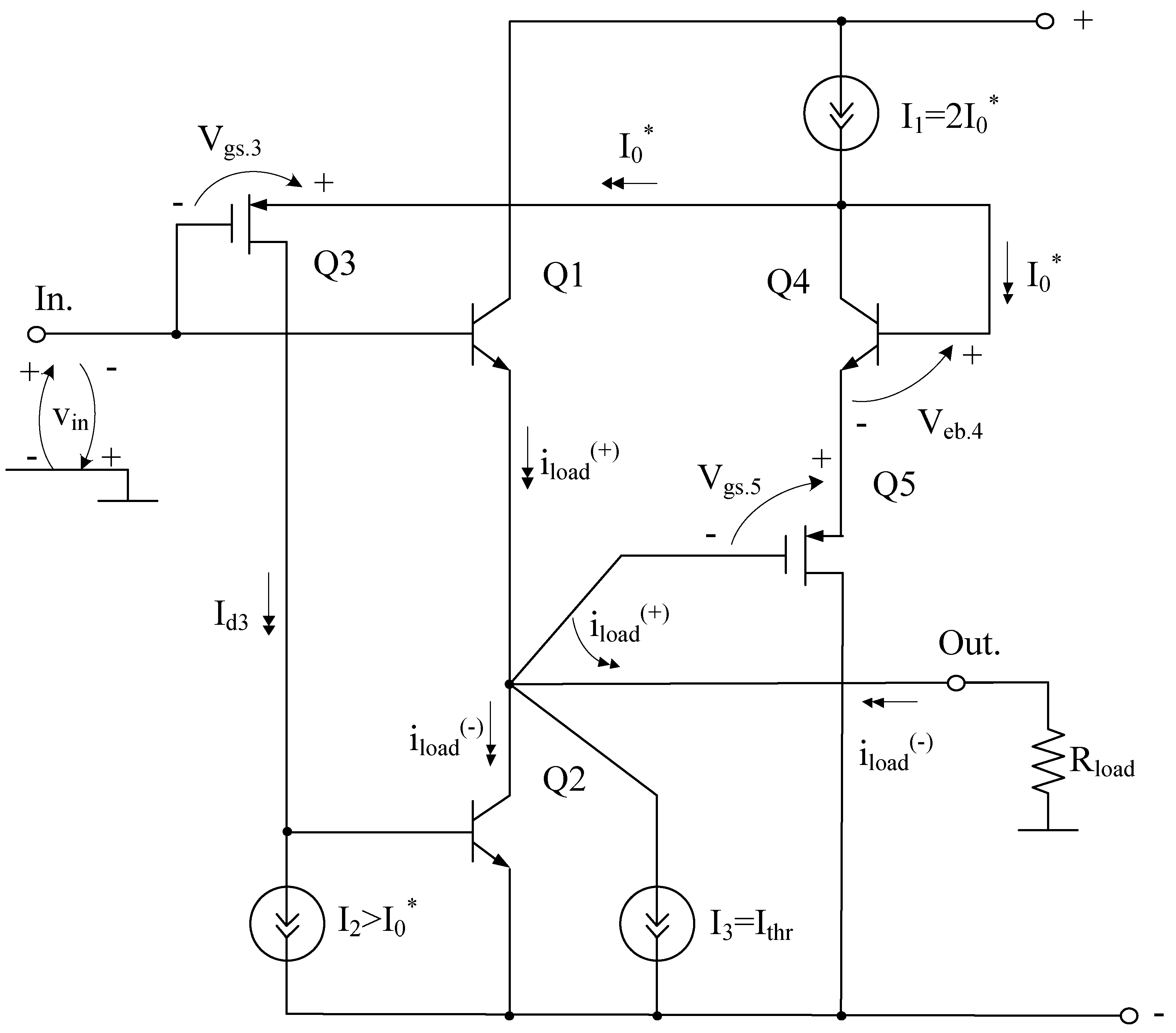
The BA static mode setting in Figure 28 is provided by selecting the currents , , .
Figure 28.
SiGe buffer amplifier: modification №21.
In this scheme, the maximum values of currents and are determined by the formulas:
where – base current gain coefficients of bipolar transistors Q1÷Q2, Q4; – maximum possible value of SS (Figure 3) output current with positive vin, – two-terminal device current I1= I2.
The feature of BA in Figure 29 is that the bipolar directions of the currents in the Rload load are here formed by the bipolar transistor Q1 and the field-effect transistor Q2.
Figure 29.
SiGe buffer amplifier: modification №22.
In these scheme maximum values of currents in the load and are determined by the formulas:
where – current gain of the base of the bipolar transistor Q1, – current of the reference current source I1, – maximum drain current of the field-effect transistor Q2.
The BA circuit in Figure 30 provides inverting amplification of the input signal. Its peculiarity is that it is realized only on SiGe bipolar transistors and has low supply voltages. The BA is tuned by selecting resistors R1 and R2.
Figure 30.
SiGe inverting buffer amplifier: modification №23
In this case, the currents and are determined by the formulas:
where – base current gain coefficients of bipolar transistors Q1÷Q3, – maximum possible value of SS (Figure 3) output current with negative vin, – value of current passing through the resistor R1.
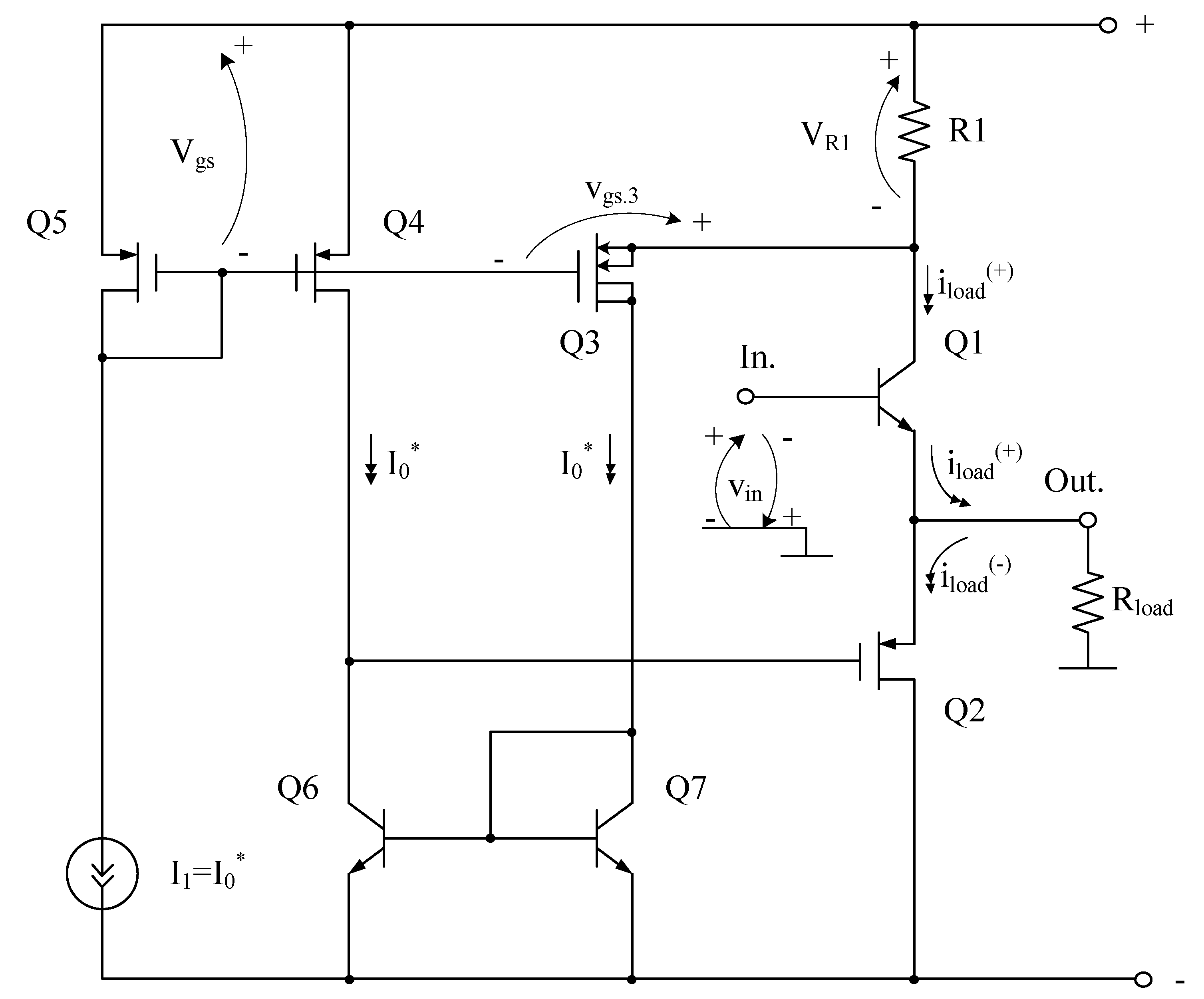
In the BA circuit (Figure 31), the field-effect transistors Q1, Q3, Q4 and Q5 provide control of the bipolar transistor Q2 at negative input signals. The BA circuit is configured by selecting the currents I1, I2.
Figure 31.
SiGe buffer amplifier: modification №24.
In this circuit, the maximum values of the currents in the load and are determined by the formulas:
where – current gain of the base of the bipolar transistor Q1, – maximum possible value of SS (Figure 3) output current with positive vin, – maximum collector current of the transistor Q2.
Conclusions
A family of buffer amplifiers (24 modifications), which are recommended to be used as output stages of micro-power SiGe Op-Amps on BiCMOS technology, is considered. A cataloging and visualization program has been developed, which allows optimizing the process of BA selection taking into account their circuitry features when designing high-temperature Op-Amps. The results of computer modeling of one of the BA circuits in Cadence simulation software are presented, which show that due to the use of SiGe BiCMOS technological process the developed circuit solutions retain their operability at temperatures up to 250 ºC.
The research has been carried out at the expense of the Grant of the Russian Science Foundation (project No. 23-79-10069), https://rscf.ru/project/23-79-10069/
References
- G. Avenier et al., "0.13μm SiGe BiCMOS technology for mm-wave applications," 2008 IEEE Bipolar/BiCMOS Circuits and Technology Meeting, Monterey, CA, USA, 2008, pp. 89-92. [CrossRef]
- T. Hashimoto et al., "A CMOS-based RF SiGe BiCMOS technology featuring over-100 GHz f/sub max/ SiGe HBTs and 0.13 /spl mu/m CMOS," Proceedings of the Bipolar/BiCMOS Circuits and Technology Meeting, Minneapolis, MN, USA, 2002, pp. 189-192. [CrossRef]
- M. Wietstruck, S. M. Wietstruck, S. Marschmeyer, S. Schulze, S. T. Wipf, C. Wipf and M. Kaynak, "Recent Developments on SiGe BiCMOS Technologies for mm-wave and THz Applications," 2019 IEEE MTT-S International Microwave Symposium (IMS), Boston, MA, USA, 2019, pp. 1126-1129. [CrossRef]
- P. Candra et al., "A 130nm SiGe BiCMOS technology for mm-Wave applications featuring HBT with fT/fMAX of 260/320 GHz," 2013 IEEE Radio Frequency Integrated Circuits Symposium (RFIC), Seattle, WA, USA, 2013, pp. 381-384. [CrossRef]
- T. Zimmer et al., "SiGe HBTs and BiCMOS Technology for Present and Future Millimeter-Wave Systems," in IEEE Journal of Microwaves, vol. 1, no. 1, Jan. 2021, pp. 288-298. [CrossRef]
- H. Rucker et al., "A 0.13µm SiGe BiCMOS technology featuring fT/fmax of 240/330 GHz and gate delays below 3 ps," 2009 IEEE Bipolar/BiCMOS Circuits and Technology Meeting, Capri, Italy, 2009, pp. 166-169. [CrossRef]
- F. Dielacher, M. F. Dielacher, M. Tiebout, R. Lachner, H. Knapp, K. Aufinger and W. Sansen, "SiGe BiCMOS technology and circuits for active safety systems," Proceedings of Technical Program - 2014 International Symposium on VLSI Technology, Systems and Application (VLSI-TSA), Hsinchu, Taiwan, 2014, pp. 1-4. [CrossRef]
- J. J. Pekarik et al., "A 90nm SiGe BiCMOS technology for mm-wave and high-performance analog applications," 2014 IEEE Bipolar/BiCMOS Circuits and Technology Meeting (BCTM), Coronado, CA, USA, 2014, pp. 92-95. [CrossRef]
- I.V. Malyshev et al., "Prospects of using SiGe BiCMOS technology to create microwave microcircuits," Problems of development of advanced microelectronic systems - 2006. Collection of scientific papers / edited by A.L. Stempkovsky. M.:IPPM RAS, 2006. pp. 191-193. (In Russian). [CrossRef]
- L. Najafizadeh et al., "SiGe BiCMOS Precision Voltage References for Extreme Temperature Range Electronics," 2006 Bipolar/BiCMOS Circuits and Technology Meeting, Maastricht, Netherlands, 2006, pp. 1-4. [CrossRef]
- K. J. Cornett, G. K. J. Cornett, G. Fu, I. Escorcia and H. A. Mantooth, "SiGe BiCMOS fully differential amplifier for extreme temperature range applications," 2009 IEEE Aerospace conference, Big Sky, MT, USA, 2009, pp. 1-10. [CrossRef]
- T. Dylan et al., "SiGe Amplifier and Buffer Circuits for High Temperature Applications," IMAPS International Conference & Exhibition on High Temperature Electronics (HiTEC 2010), USA, 2010, pp. 1-7. [CrossRef]
- M. Bellini, J. D. M. Bellini, J. D. Cressler and J. Cai, "Assessing the High-Temperature Capabilities of SiGe HBTs Fabricated on CMOS-compatible Thin-film SOI," 2007 IEEE Bipolar/BiCMOS Circuits and Technology Meeting, Boston, MA, USA, 2007, pp. 234-237. [CrossRef]
- Thomas, D.B.; et al. , "Performance and reliability of SiGe devices and circuits for high-temperature applications. Proceedings," 2009 IMAPS International Conference on High Temperature Electronics Network, HiTEN, 2009, pp 49-56.
- R. Basu, A. R. Basu, A. Singh, "High temperature Si-Ge alloy towards thermoelectric applications," A comprehensive review. Materials Today Physics, №21, pp. 1-26. [CrossRef]
Disclaimer/Publisher’s Note: The statements, opinions and data contained in all publications are solely those of the individual author(s) and contributor(s) and not of MDPI and/or the editor(s). MDPI and/or the editor(s) disclaim responsibility for any injury to people or property resulting from any ideas, methods, instructions or products referred to in the content. |
© 2025 by the authors. Licensee MDPI, Basel, Switzerland. This article is an open access article distributed under the terms and conditions of the Creative Commons Attribution (CC BY) license (https://creativecommons.org/licenses/by/4.0/).
Copyright: This open access article is published under a Creative Commons CC BY 4.0 license, which permit the free download, distribution, and reuse, provided that the author and preprint are cited in any reuse.


