
Submitted:
12 July 2023
Posted:
13 July 2023
You are already at the latest version
Abstract
Digital-based differential amplifiers (DDA) are particularly suitable to low voltage digital integrated circuit technologies. This paper presents an exhaustive analysis of the digital-based analog amplifiers to take advantage of today's high-performance digital technologies and of computer-aided design (CAD) commonly employed to design integrated circuits. The operating principle and the main mathematical relations of the digital-based differential amplifiers are discussed along with an exhaustive explanation of its operating regions and of the corresponding power consumption. Finally, a detailed description of the design procedure of in UMC 180nm standard CMOS technology is shown.
Keywords:
Digital-based amplifiers
; analog integrated circuits
; amplifiers
; ultra low voltage
; ultra low power
1. Introduction
Ubiquitous electronic requires compact ultra-low power devices and fast prototypization. Technology scaling favors digital circuits thanks to their high speed and low power dissipation. In this context, it is rising the trend of implementing low-voltage inverter-based analog circuits. The elementary inverter-based amplifier is a couple of CMOS digital inverters that operates in an analog fashion due to the common-mode (CM) voltage that keeps both the NMOS and PMOS transistors in the saturation region. The resulting amplifiers have high differential gain, large transconductance, high output resistance, and high gain bandwidth (GBW). The gain of the simple inverter is the ratio of the small signal transconductances and output conductances: , where is the transconductance and the output conductance. Unfortunately, operating the inverter as an analog amplifier, leads to large variation with temperature and fabrication process of the DC gain and GBW. Furthermore, the higher is the voltage gain, the narrower is the range of the CM. To face these issues several techniques were proposed in the literature, mostly based on common mode feedback (CMFB) circuits, that sense the output CM to control the bias current of the inverter. Indeed, , , and , depend on the drain and source voltages and, in turn, on the CM. Therefore, the DC gain can be regulated by changing the CM. In principle, only two resistors are required to extract the CM. The CMFB can be also implemented without resistors as in the Nauta operational transconductance amplifier and its most recent derivations [1]-[5]. Nevertheless, they remain analog circuits in which both the NMOS and PMOS are in saturation, the current flows continuously, and the static power consumption is large. Several approaches, based on current-starved topologies, were suggested in the literature to reduce the power consumption: they are fully differential circuits that need an output common mode voltage feedback to stabilize the small signal performances.
Another approach is to radically re-think analog functions in digital terms to use only digital circuits as, by the way of example, the class D amplifier [6]. VCO-based amplifiers [7], voltage to time converters [8], digital.-to-analog converters [9], hybrid analog-digital amplifiers [10] and digital-based amplifiers [11] - [19] are reported in the literature. In [11]-[19] a differential amplifier, composed of logic gates only, is shown. It has several appealing features: low power consumption, small area, easy design, and fast prototyping. It is an interesting approach and a deep understanding of the possible topologies, design, features, and limits is important for analog-background designers that, habitually, use different design methodologies. This paper is focused on the understanding of the DDA both from a circuital and mathematical standpoint with particular emphasis on the power consumption that is one of its main appealing features. In section II, the operating principles, the transistors operating conditions, and the main mathematical relations to design the DDA are devised. In section III, the full design of the amplifier in 180nm CMOS standard is shown, along with a comprehensive explanation of the operating regions and power consumption. In section IV, some conclusions are drawn.
2. Operating Principle of the DDA
In Figure 1 the building blocks of the DDA are shown [11]. The output of the digital buffers (, ) is high (H) when the input voltages , are larger than the threshold voltage () and low (L) when are lower than . The CMFB (green box) adjusts the CM voltage in order to emulate the input stage of a differential amplifier. Hence, (, ) are related to the differential voltage = . A detailed description of the DDA, along with the basic mathematical relations, are reported in [11]. For the sake of clarity, here we recall: , and, using a balanced resistor network, .
Since the logic gates are assumed to switch much faster than the input signals of the DDA, the output and CMFB voltages e are well approximated by the following first order differential equations:
where if , if , 0 elsewhere }, if , if , 0 elsewhere }, , and and represent the propagation time through the logic gates. Furthermore, for the sake of simplicity, the logic gates are assumed ideal with the same propagation time , and , constant and not depending on and . Under those assumptions, in the following, the two possible operating conditions = 0 and 0, will be discussed.
In Figure 2, the waveforms when = 0 are shown. When = 0, , are the same, the output inverter is in high impedance, is constant and the load capacitor holds its charge. Nevertheless, the compensation voltage oscillates, in fact:
- At both and cross , and , switch from L to H. It takes a certain amount of time for the signal to propagate through the CMFB.
- Before , although , are high, the CM compensation inverter has not yet changed its state, and is still charging with as when .
- At , the CMFB changes its state: the pull-down switches on, and the capacitor is discharged with a constant current .
- From to , while is discharging, both and fall below the threshold .
- At , , switch from H to L;
- Before the CM compensation inverter has not yet changed its state and is still discharging.
- At the CM compensation inverter changes state, the pull-up switches on, and the capacitor is charged with the current .
- This cycle is repeated every .
Hence, the delay introduced by the compensation network induces a triangular wave oscillation on of period and peak-to-peak amplitude .
In Figure 3, the waveforms when are shown, similar considerations hold when .
- The differential voltage corresponds to a small mismatch between and that, in turn, causes to cross the threshold voltage with a small delay ; during , the differential voltage is positive, , and the outputs (, ) = (). After , it is , that crosses the threshold voltage with a small delay respect to .
- is a triangular wave with the same period , as in Figure 2 but, during the interval , the voltage is clamped since the buffer is in the high impedance region.
- During the interval , the output buffer charges and steps up of .
- The charge on is incremented by , twice every .
In other words, the DDA operates as a double conversion from voltage to time and back from time to voltage again. The first conversion is to , thanks to the oscillation on . Indeed, the mismatch on and is converted into a delay , i.e. a time. Then, the output buffer converts the delay back into a voltage . The voltage gain of the DDA in the frequency domain, assuming only the capacitive load , reads:
where ,
and is the phase shift due to the propagation delay . Furthermore, when , eq. (2) can be simplified as . Thus, the transfer function is equivalent to an integrator with a unity gain frequency of . The digital-based analog amplifier can be used, almost as conventional analog amplifiers, in feedback loops. Nevertheless, the classical assumptions of infinite input impedance () and negligible output impedance () are not properly verified. The transfer function can be approximated as:
where is the gain of the feedback network set by the resistors’ ratio. In other words, the DDA operates as a first order system.
3. Design and Simulations of the DDA
The digital-based amplifier discussed in the previous section has been designed in the standard 180nm UMC (United Microelectronic Corporation) CMOS process and extensively simulated in different operating conditions. It is worth noting that the final schematic is slightly modified with respect to the base circuit of Figure 1 to equalize the propagation time of and .The circuit is extremely simple, composed only of resistors and logic gates. The supply voltage is standard for this technology (1.8V) at the aim of investigate the DDA in normal operating conditions. Several simulations worked out at lower supply voltages show that the DDA operates correctly at supply as low as 400mV.
3.1. Sizing of the DDA in UMC 180 nm CMOS Process
The first step is to dimension the CMOS inverter with a logic threshold half of . Considering the different transistor’s threshold and mobility , the ratio of the PMOS and NMOS, to maximize the symmetry of the inverter, results of 4.725. Minimum transistors are chosen to minimize the gate capacitance: nm, nm and nm. The NOR logic gate is composed of two PMOS connected in series and two NMOS in parallel. To have a symmetric behavior both the transistors of the pull-up and pull-down read: nm, nm and nm. Dual considerations hold for the NAND that comprises two PMOS in parallel and two NMOS in series: nm, nm and nm. The input resistors R1-R4, on the one hand, should be large to have a high input impedance, on the other hand should be not too large to limit the area consumption and the thermal noise. Although same resistances of 145k were chosen to have an input differential impedance of 580k, in the layout were slightly modified to have true rail-to-rail common mode: = 140k and = 150k. The output and the CMFB are dimensioned to balance the propagation delay between the logic gates. The dimensions of the output stage are: nm, m and m. And for the inverter of the CMFB is: nm, nm and nm. All the dimensions are in agreement to the technology minimum grid.
3.2. Simulation Results
The DDA can hardly be simulated by means of the classical small-signal AC analysis tools since the core of its operating principle is digital and is related to the oscillation of . Time-expensive transient analysis are required to design and characterize the amplifier. The DDA was simulated in two different configurations: open loop as a comparator, and closed loop as a feedback amplifier.
3.2.1. Open Loop
The amplifier is operated as a comparator. In the simulations, to generate a modulated differential voltage that emphasizes all the different operating regions of the amplifier, we used two input sinusoidal signals and of amplitude with different frequencies: 10kHz, 30kHz. The transient simulation time is 100s. The waveforms of the most relevant voltages of the internal nodes are shown in Figure 4: the bottom x-axis represents the simulation time, the top x-axis the operating regions, the y-axis the voltages at the nodes. In Figure 5, one can see that the DDA has five distinct behaviors and power consumption that we call operating regions 1-5:
-
In the regions 1 and 5, the differential voltage is large, are well separated and opposite with respect to the logic threshold . In these regions the output voltage saturates to or 0, the common-mode compensation network is not active and only the pull-up or the pull-down of output inverter turns on. In Figure 4, , are the gate voltages of the pull-up and pull-down respectively. In Figure 5, the regions 1 and 5 are limited by the equations and :Furthermore, since the CMFB is not active , i.e. ( + )/2, the regions 1 and 5 reads:
- In the region 3, the differential voltage is small enough to activate the CMFB. The compensation voltage oscillates and the digital outputs and commute between L and H. Both the pull-up and the pull-down of the output inverter are active: if is positive, steps up, if is negative, steps down. This region is defined by the condition i.e.
- In the regions 2 and 4, the differential voltage is small, but not as small as in the region 3. In the region 2 , holds the low logic state, while quickly commutes from H to L due to the CMFB. The pull-down of the output stage switches on. In the region 4 , holds the low logic state, while quickly commutes from H to L due to the CMFB. The pull-up of the output stage switches on. Hence, the pull-up or the pull-down switches on, but are not always active as in region 1 and 5.
The power consumption of the DDA is mostly dynamic and is due to the switching of the gates (), to the charging and discharging of () and (). It strongly depends on the operating regions of the amplifier as shown in Figure 5: the dissipated power, as a function of the differential voltage, is represented as a shade of blue from light (lower power consumption) to dark (higher power consumption). The x- and the y-axis are the input voltages , ranging from 0 to in steps of 50mV. It is worth adding, that the simulations are worked out at 1.8V (standard for this technology): if the voltage supply is reduced, the power consumption gets remarkably smaller, [13]-[16]. This is due both to the dependence of the dynamic power on and to the reduction of the switching frequencies of the CMFB and of the output stage. In the regions 1 and 5, the power dissipation is lower than in the region 2, 3, 4, since the common mode compensation network is always switched off, only the pull-up or pull-down is conducting, and the output voltage saturates to or 0. In the regions 2 and 4 the power dissipation is higher since the CMFB is active. Finally in the region 3 the power consumption reaches its maximum since the differential voltage is small and oscillates continuously.
3.2.2. Closed Loop
The DDA can be used in feedback connection as an analog amplifier. In the simulations of the closed loop connection a sinusoidal rail-to-rail input signal of 20kHz is applied to the non-inverting input . The simulation time is 100s. The Fast Fourier Transform (FFT) of the buffer connection with unitary loop gain (G) is 0.992, the phase delay () 0.08o, and a total harmonic distortion (THD) 0.23%. Figure 6 show that, when the DDA is used as a buffer, the differential voltage is very small and always operates in the region 3. Hence, despite the rather good overall performances, the power consumption reaches its maximum.
Furthermore, the closed loop configuration was simulated in several other configurations. Figure 7 shows the simulations in three different configurations: buffer (G=0.987, =0.14o, THD=0.31% ), inverter (G=-0.938, =0.06o, THD=1.58%), and gain two (G=2.007, =0.06o, THD=0.99%). The results are shown in Figure 7. Simulations are worked out with an input signal of 400mVp and a frequency of 20kHz. The voltage gain G and the output voltage are close to the ideal ones while the largest THD is smaller than 1.6%, the phase delay is below 0.14o, and the larger offset 33.7 mV only.
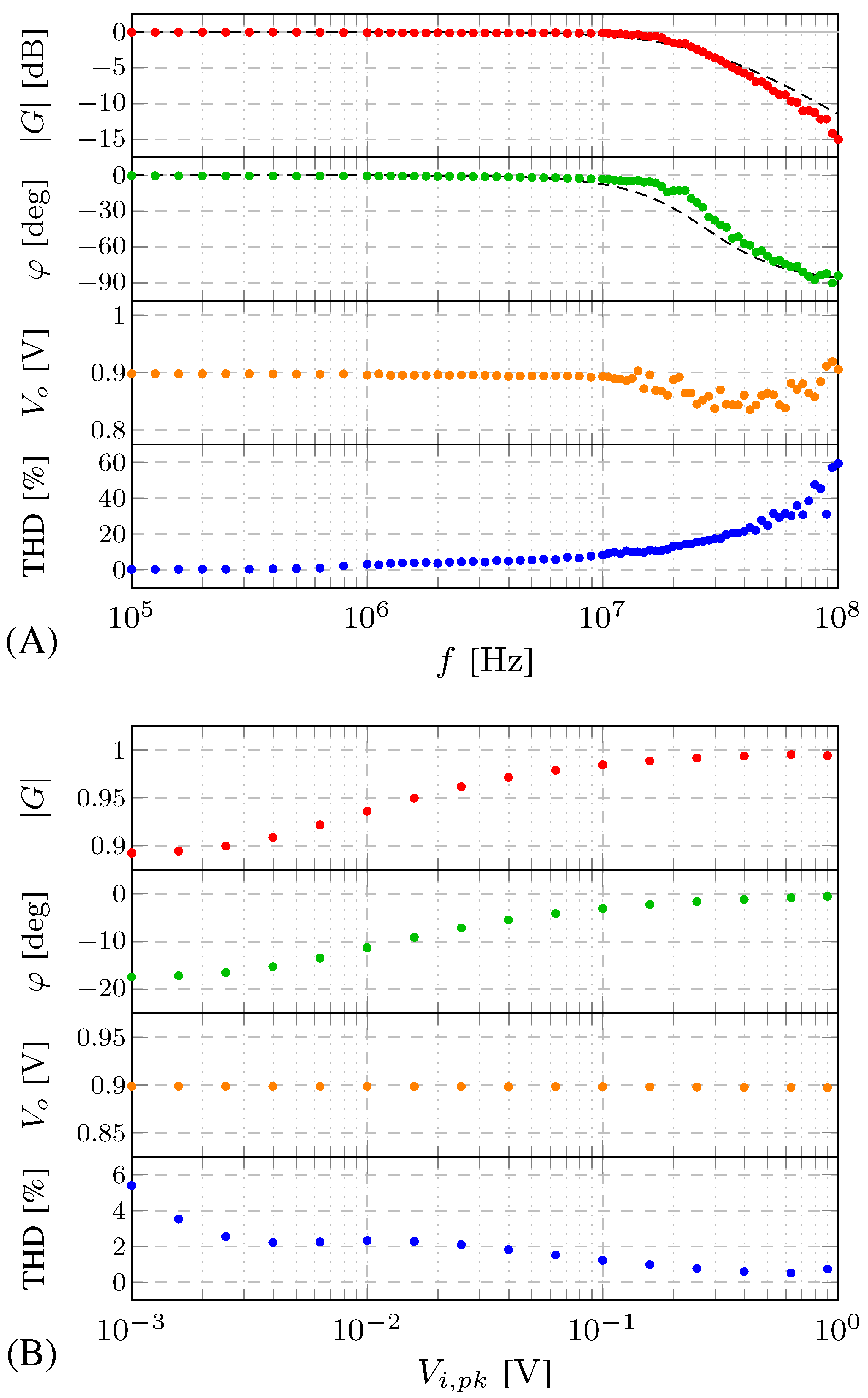
Finally, the closed loop amplifier is simulated with rail-to-rail input voltages at several frequencies. In Figure 8 (A) the FFT in the range of 100kHz-100MHz is shown.
The amplifier act as a single pole dominant system with a unity gain frequency of about 27.6MHz. The output voltage (gain and phase) is almost ideal up to 10MHz, while the THD starts rising at a lower frequency: about 1MHz. It is worth stressing that simulations are worked out at 1.8V. Nevertheless, one of the most appealing feature of the DDA is the small power consumption and lower are often used: in that case, the overall performance degrades rather quickly. Finally, simulations were worked out by changing the amplitude of the input voltage at constant frequency (500kHz), i.e. within the bandwidth of the amplifier. The results are shown in Figure 8 (B), for an input signal ranging from 1mV up to 900mV. One can see that the DDA works very well when the amplitude of the input signal is large enough and slightly deteriorates as input voltage gets lower and lower. The resistive compensation network, in fact, limits the input impedance of the amplifier. In several applications, such as biomedical, wearable, IoT and sensoring, these limits do not represent a real drawback, and the DDA is a very promising architecture. High frequencies or low input signals represent the most important limit of the DDA that require some adjustments. To this aim, a more recent DDA architecture [16,19] with a new compensation network based on floating inverters, was reported. Thanks to this new common mode compensation circuit, the DDA in [16,19] can amplify low amplitude signals with very good overall performances.
4. Conclusions
The digital-based analog amplifier was designed and investigated along with its main mathematical relations. We have shown that the amplifier can operate in 5 different regions and that the power consumption peaks when is small. Several simulations were worked out both in the open and closed loop configuration. The simulations show that the amplifier represents a really attractive approach for the signal conditioning of the integrated circuits with advantages on power consumption and ease of design. The amplifier is better suited for low to medium frequency input signals with rather large amplitude. Nevertheless, it represent a very appealing architecture when the area on chip and the power dissipation are of paramount importance.
Author Contributions
All the authors have contributed substantially to the paper. Anna Richelli, Luigi Colalongo have supervised the work, have provided the simulation tools and have written the paper; Paolo Faustini is graduated-five years Laurea degree- student and Andrea Rosa is PhD student, they have investigated on the power consumption of the amplifier and performed the simulations.
Conflicts of Interest
The authors declare no conflict of interest.
Abbreviations
The following abbreviations are used in this manuscript:
| DDA | Digital-based Differential Amplifier |
| CAD | Computer-aided Design |
| UMC | United Microelectronics Corporation |
| CMOS | Complementary Metal Oxide Semiconductor |
| CM | Common Mode |
| GBW | Gain Bandwidth |
| CMFB | Common Mode Feedback |
| DC | Direct Coupling |
| VCO | Voltage Controlled Oscillator |
| FFT | Fast Fourier Transform |
| G | Loop Gain |
| THD | Total Harmonic Distortion |
| IoT | Internet of Things |
References
- B. Nauta, "A CMOS transconductance-C filter technique for very high frequencies," IEEE Journal of Solid-State Circuits, vol. 27, no. 2, Feb. 1992.
- Rodovalho, L.H.; Toledo, P.; Mir, F.; Ebrahimi, F. Hybrid "Inverter-Based Fully Differential Operational Transconductance Amplifiers", Chips 2023, 2, 1-19.
- A. P. Nicholson, A. Iberzanov, J. Jenkins, T. J. Hamilton and T. Lehmann, "A Statistical Design Approach for a Digitally Programmable Mismatch-Tolerant High-Speed Nauta Structure Differential OTA in 65-nm CMOS," in IEEE Transactions on Very Large Scale Integration (VLSI) Systems, vol. 24, no. 9, pp. 2899-2910, Sept. 2016.
- Manfredini, G.; Catania, A.; Benvenuti, L.; Cicalini, M.; Piotto, M.; Bruschi, P. "Ultra-Low-Voltage Inverter-Based Amplifier with Novel Common-Mode Stabilization Loop", Electronics 2020, 9.
- J. Wei, Y. Yao, L. Luo, S. Ma, F. Ye and J. Ren, "A Novel Nauta Transconductor for Ultra-Wideband gm-C Filter with Temperature Calibration," 2019 IEEE International Symposium on Circuits and Systems (ISCAS), Sapporo, Japan, 2019.
- F. Guanziroli, R. Bassoli, C. Crippa, D. Devecchi, and G. Nicollini, “A 1 W 104 dB SNR filter-less fully-digital open-loop class D audio amplifier with EMI reduction,” IEEE Journal of Solid-State Circuits, vol. 47, no. 3, Mar. 2012.
- S. Kalani, A. Bertolini, A. Richelli and P. R. Kinget, "A 0.2V 492nW VCO-based OTA with 60kHz UGB and 207 μVrms noise," 2017 IEEE International Symposium on Circuits and Systems (ISCAS), Baltimore, MD, USA, 2017.
- A. Richelli, L. Colalongo, Zs. M. Kovacs-Vajna, "EMI Effect in Voltage-to-Time Converters", IEEE Transactions on Circuits and Systems II: Express Briefs, Vol. 8, No. 4, Apr. 2021.
- R. Rubino, F. Musolino, Y. Chen, A. Richelli and P. Crovetti, "A 880 nW, 100 kS/s, 13 bit Differential Relaxation-DAC in 180 nm," 2023 18th Conference on Ph.D Research in Microelectronics and Electronics (PRIME), Valencia, Spain, 2023, pp. 269-272.
- M. Privitera, P. S. Crovetti and A. D. Grasso, "A novel Digital OTA topology with 66-dB DC Gain and 12.3-kHz Bandwidth," in IEEE Transactions on Circuits and Systems II: Express Briefs. [CrossRef]
- P. Crovetti, "A digital-based analog differential circuit," IEEE Transactions on Circuits and Systems I: Regular Papers, vol. 60, no. 12, Dec. 2013.
- Palumbo, G.; Scotti, G. "A Novel Standard-Cell-Based Implementation of the Digital OTA Suitable for Automatic Place and Route", J. Low Power Electron. Appl. 2021, 11, 42. [Google Scholar] [CrossRef]
- P. Toledo, P. Crovetti, O. Aiello and M. Alioto, "Fully Digital Rail-to-Rail OTA With Sub-1000-μm2 Area, 250-mV Minimum Supply, and nW Power at 150-pF Load in 180 nm," in IEEE Solid-State Circuits Letters, vol. 3, pp. 474-477, 2020.
- P. Toledo, P. Crovetti, O. Aiello and M. Alioto, "Design of Digital OTAs With Operation Down to 0.3 V and nW Power for Direct Harvesting," in IEEE Transactions on Circuits and Systems I: Regular Papers, vol. 68, no. 9, pp. 3693-3706, Sept. 2021.
- P. Toledo, P. Crovetti, H. Klimach, S. Bampi, O. Aiello and M. Alioto, "A 300mV-Supply, Sub-nW-Power Digital-Based Operational Transconductance Amplifier," in IEEE Transactions on Circuits and Systems II: Express Briefs, vol. 68, no. 9, pp. 3073-3077, Sept. 2021.
- P. Toledo, P. S. Crovetti, H. D. Klimach, F. Musolino and S. Bampi, "Low-Voltage, Low-Area, nW-Power CMOS Digital-Based Biosignal Amplifier," in IEEE Access, vol. 10, pp. 44106-44115, 2022.
- P. Toledo, O. Aiello and P. S. Crovetti, "A 300mV-Supply Standard-Cell-Based OTA with Digital PWM Offset Calibration," 2019 IEEE Nordic Circuits and Systems Conference (NORCAS): NORCHIP and International Symposium of System-on-Chip (SoC), Helsinki, Finland, 2019.
- P. Toledo, P. Crovetti, H. Klimach and S. Bampi, "A 300mV-Supply, 2nW-Power, 80pF-Load CMOS Digital-Based OTA for IoT Interfaces," 2019 26th IEEE International Conference on Electronics, Circuits and Systems (ICECS), Genoa, Italy, 2019, pp. 170-173.
- R. Rubino, S. Carrara and P. Crovetti, "Direct Digital Sensing Potentiostat targeting Body-Dust," 2022 IEEE Biomedical Circuits and Systems Conference (BioCAS), Taipei, Taiwan, 2022.
Figure 1.
Digital-based amplifier [11], resistor network (yellow box), digital buffers (pink box), blue box (output stage), CMFB (green box).
Figure 1.
Digital-based amplifier [11], resistor network (yellow box), digital buffers (pink box), blue box (output stage), CMFB (green box).
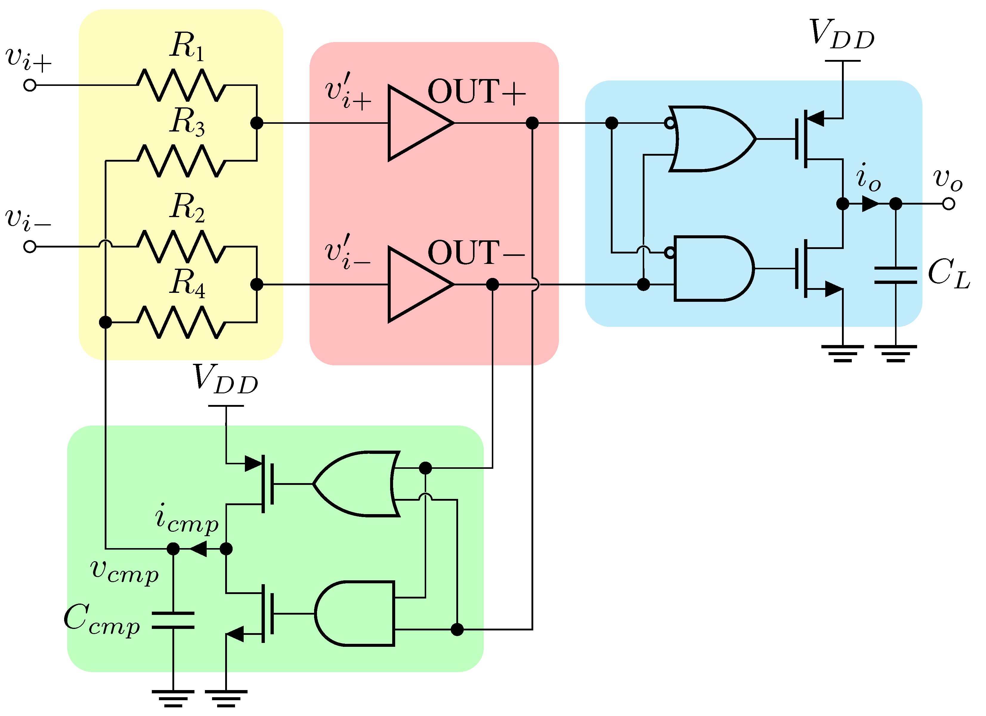
Figure 2.
Waveforms of the DDA at .
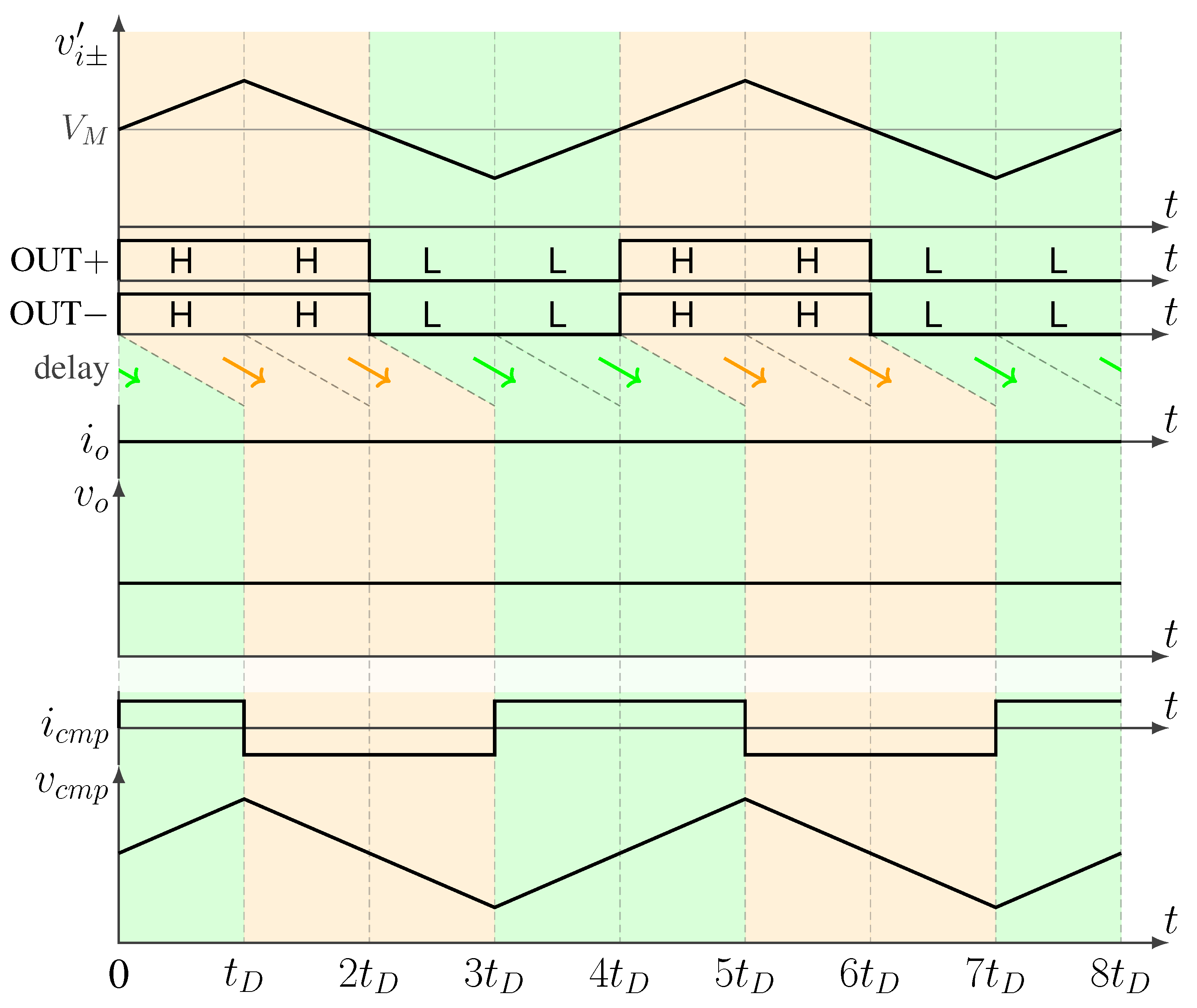
Figure 3.
Waveforms of the DDA at .
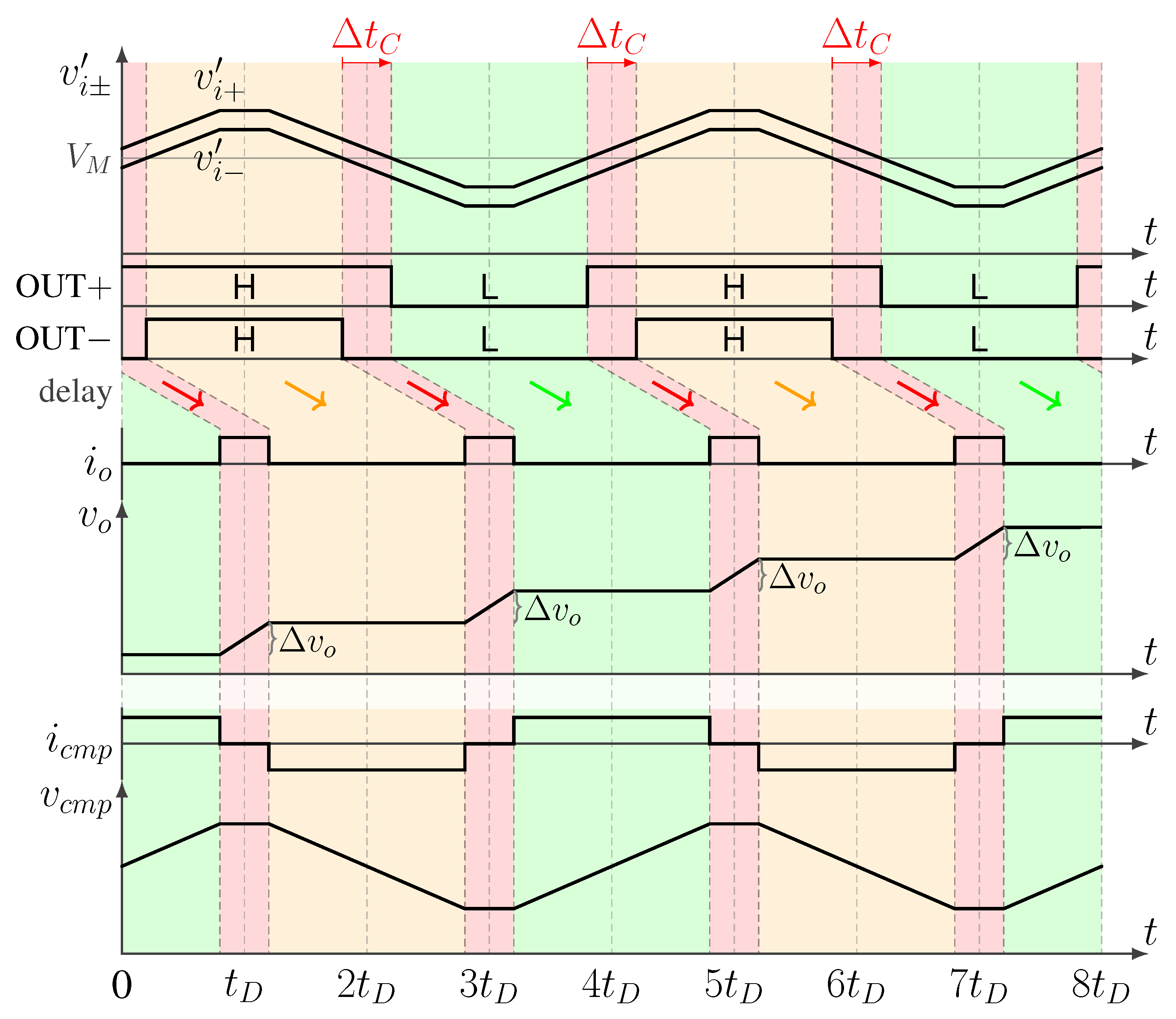
Figure 4.
Open loop: input/output waveforms and intermediate node voltages
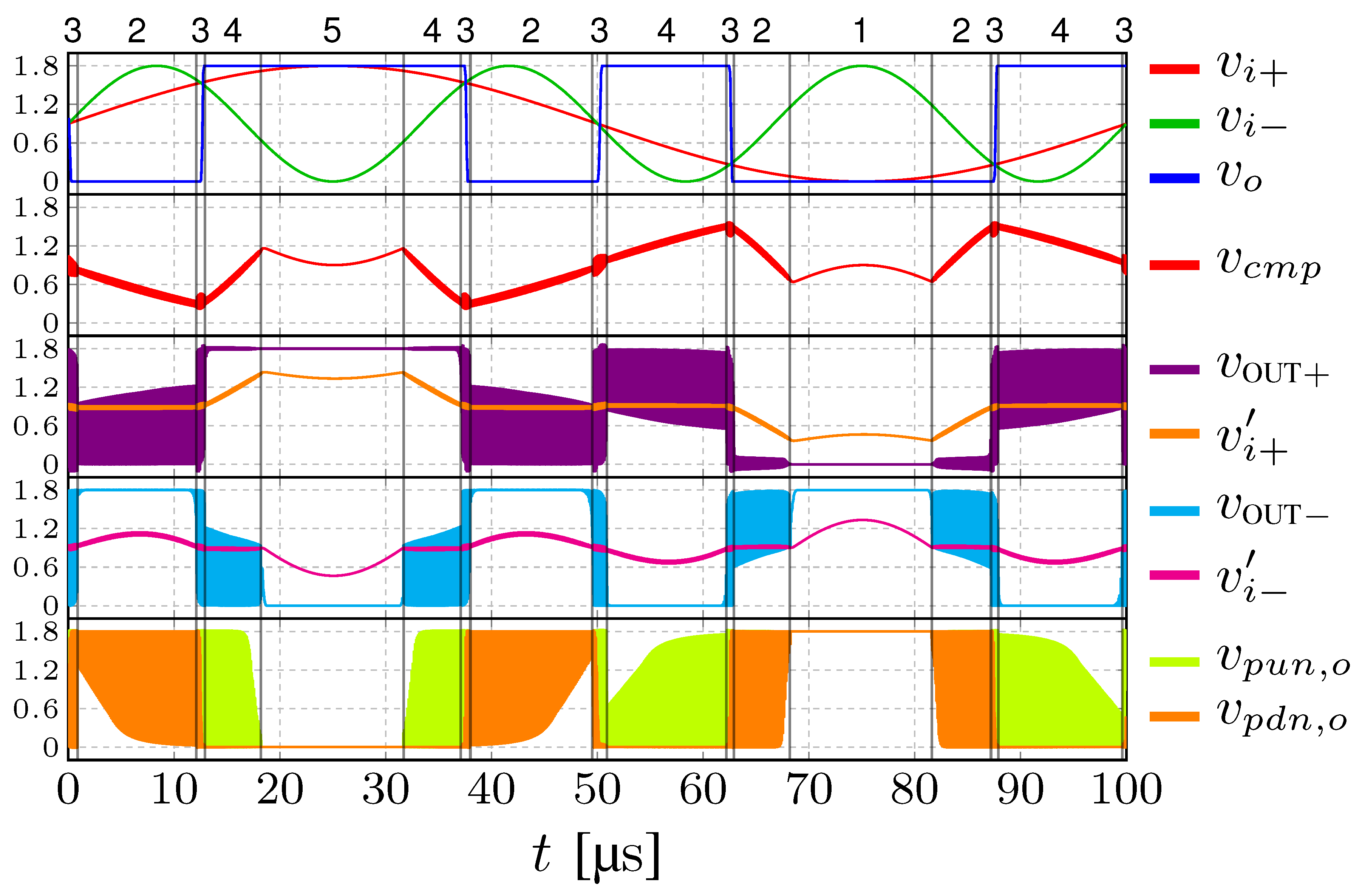
Figure 5.
Open loop: operating regions vs. and power consumption
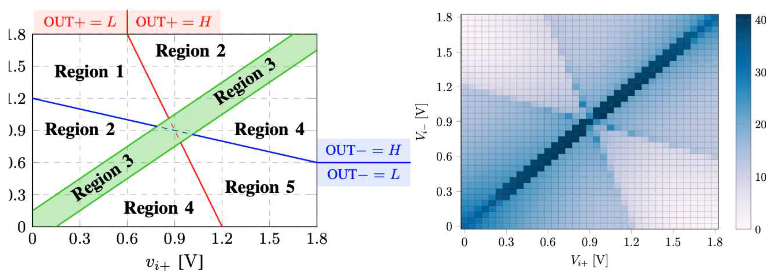
Figure 6.
Buffer: input/output waveforms and internal node voltages
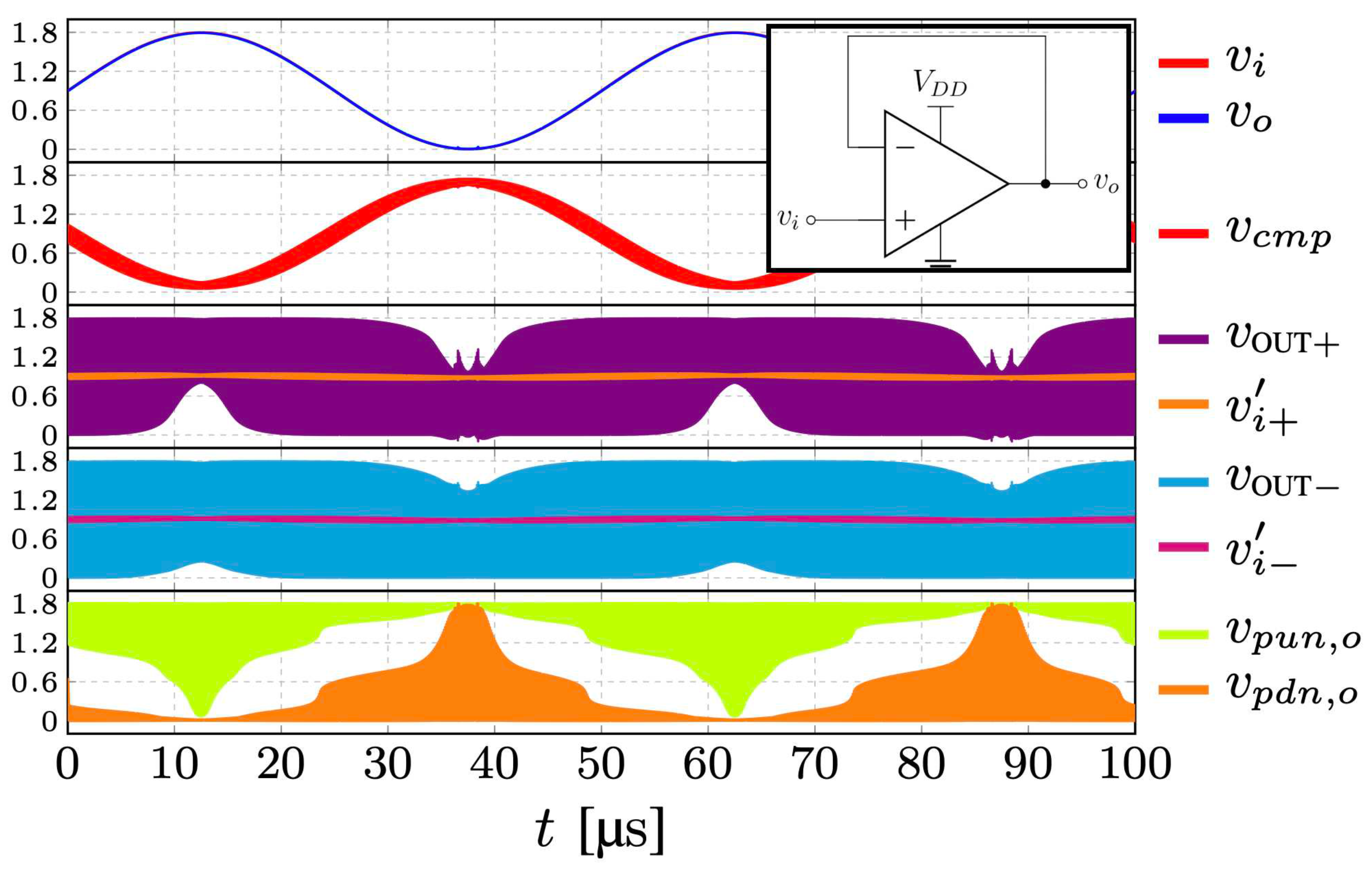
Figure 7.
Closed loop simulations
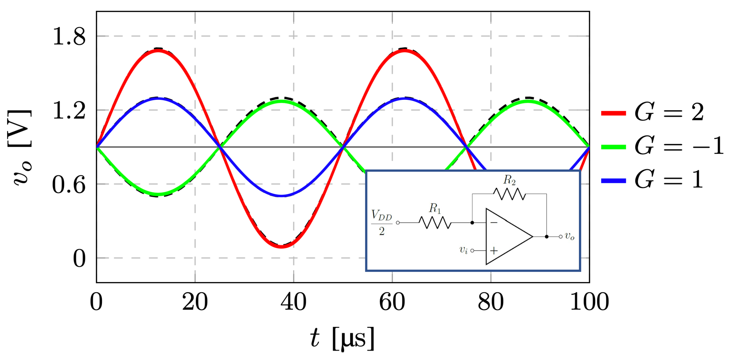
Figure 8.
Buffer: G, , output voltage, and THD as a function of frequency (A), and of the input signal amplitude (B)
Figure 8.
Buffer: G, , output voltage, and THD as a function of frequency (A), and of the input signal amplitude (B)
Disclaimer/Publisher’s Note: The statements, opinions and data contained in all publications are solely those of the individual author(s) and contributor(s) and not of MDPI and/or the editor(s). MDPI and/or the editor(s) disclaim responsibility for any injury to people or property resulting from any ideas, methods, instructions or products referred to in the content. |
© 2023 by the authors. Licensee MDPI, Basel, Switzerland. This article is an open access article distributed under the terms and conditions of the Creative Commons Attribution (CC BY) license (http://creativecommons.org/licenses/by/4.0/).
Copyright: This open access article is published under a Creative Commons CC BY 4.0 license, which permit the free download, distribution, and reuse, provided that the author and preprint are cited in any reuse.


