Submitted:
14 April 2025
Posted:
15 April 2025
You are already at the latest version
Abstract
This work presents the results of studies of wear-resistant coatings obtained on carbon steel 45 by electrospark deposition (ESD). Multicomponent powder compositions were used, containing WC, Co-Ni-Cr-B-Si semi-self-fluxing alloys and additives of the super-hard compounds B4C and TiB2 with different ratios between the individual components. The ESD electrodes were created using the powder metallurgy methods. The selection of coating compositions and studies were carried out with the aim of obtaining coatings with increased adhesion to the substrate and improved physicochemical and tribological properties under conditions of friction. Coatings with crystalline-amorphous structures, with newly formed intermetallic and wear-resistant phases, and with thickness, rough-ness and microhardness varying depending on ESD modes in ranges respectively δ=8÷50µm Ra=1.5÷5 µm, and HV 8.5÷15.0 GPa were obtained. The ratios between the in-dividual components in the composition of the electrode material and the ESD conditions have been specified, under which the maximum improvement of the properties and wear resistance of the coatings has been obtained - up to 4÷5 times higher than that of the sub-strate and up to 1.5 times higher than that of used conventionally WC-Co electrodes. The relationship of the wear with the ratios between the components in the coating composi-tions has been established.
Keywords:
Electrospark Deposition (ESD)
; phase composition
; coatings
; roughness
; microhardness
; carbides
; nitrides
; borides
; wear resistance
1. Introduction
Wear-resistant coatings are a technically and economically viable way to strengthen and regenerate the surfaces of machine elements subjected to intense wear. The numerous operating and friction conditions under which wear occurs have led to the creation of numerous technologies and methods for applying coatings. However, the applications of most of these technologies are often associated with a number of technological difficulties and limitations due to reasons such as expensive and energy-intensive equipment, complex technologies requiring significant investments, heating of the parts leading to recrystallization and thermal deformation, insufficient adhesion and thickness of coatings, the need for subsequent surface treatment, unsuitability for strengthening a wide range of working elements with different masses and configurations, etc.
The above difficulties and limitations can be overcome by the electrospark deposition (ESD) method, which is much cheaper and easier than the other methods, does not require large investments and additional infrastructure, and its wide versatility, simplicity, flexibility and high efficiency allow its successful use for obtaining wear-resistant coatings on any metal parts, tools and parts in all industrial sectors [1,2,3]. The most significant advantages of ESD over other methods are low energy consumption and cost, high adhesion strength to the substrate, the absence of heating and deformation of the coated product, the simplest, easiest, and most universal technology, the possibility of local application of coatings on any surfaces, even those with the most complex shape, the possibility of operation without additional treatment of the modified surfaces, and the high environmental friendliness [2,4,5]. ESD is based on the use of pulsed discharges with controlled energy and duration of 10-6–10-5 s. As a result, electrical erosion and polar transfer of material from the deposition electrode (anode) to the product (cathode) occurs. The pressure of the shock wave from the action of the electric spark is from 2.106 to 7.106 MPa, the temperature of the electrode surface reaches 5.103 to 1.104 °C [5,6,7,8]. The intensity of the electric field during ESD is 107 -109 W/cm2 [2,5,6,7,8], which is much higher than the critical intensity at which the anode material melts. As a result, the explosively molten electrode material is transferred onto the cathode surface in liquid, solid (softened) and vapor phases with extremely high particle velocity [1,2,3,4,5,7,8,9]. They mix with the locally melted micro-spot of the substrate and a surface layer of a mixture of the two materials is formed, new compounds and phases resulting from their chemical interaction and from reactions with the environmental elements. According to many researchers, the short duration of the ESD process and the extremely high heating rates up to 104 °C and cooling rates (up to 105 -106 °C/s) [1,2,5,6,8,9,10,11,12], allow the formation of new ultradisperse, amorphous and nanoscale wear-resistant structures [1,2,5,6,7,9,10,11,13,14,15,16,17].
The heat-affected zone is small, resulting in minimal thermal and metallurgical changes. The layer has increased adhesion to the substrate, as it is formed by mixing the molten materials of the processing electrode (anode) and the substrate (cathode) [1,2,3,4,5,6,7,8] and increased hardness, tribological and corrosion properties, which are controlled in a wide range by changing the parameters of the spark discharge and the composition of the electrode material.
For electrodes in ESD, a wide range of metals and metal alloys [1,2,3,5,8,9,10,14,16,17,18,19,20] and classic hard alloys based mainly on WC-Сo, WC+TiC–Сo, etc. [1,2,3,4,5,12,15,19,21,22,23,24,25,26,27] are usually used. Metals and alloys have high strength and ductility and provide good adhesion to the base and higher thickness and density of the coating, but have limited hardness and wear resistance [1,2,3,4,5,8,9,10,13,14]. The hard alloy coatings have high hardness and wear resistance, but also high brittleness, which does not allow the use of high-energy pulses due to the deterioration of the quality of the coatings [1,2,3,4,5,6,15,19,21,22,23,24,25] and in many cases limits the desired effect in a number of applications.
It is obvious that further enhancement of the ESD effect is associated with obtaining coatings from harder and more wear-resistant materials that provide an increase in both thickness, adhesion and uniformity, as well as hardness, elasticity, strength and wear resistance of the obtained coatings. The data from numerous studies show [1,2,5,15,17,19,25] that such a complex of balanced contradictory properties can be achieved by composite multicomponent and multiphase coatings consisting of several highly wear-resistant materials—and a solder mass also from several metals or metal alloys. The many components allow using the advantages of each of them, as well as new ones obtained from their combination and from chemical reactions and between them, the substrate and environmental elements and to provide better characteristics and properties of the coating compared to that when using conventional hard alloys. Multicomponent coatings are a modern trend in new technologies, which is intensively developing and expanding [1,2,5,12,17,18,23,25,28,29,30,31,32]. The mixtures of materials with high hardness and wear resistance with lower melting metals allow to obtain coatings firmly connected to the base, with high hardness and wear resistance, and at the same time high strength provided by the metal matrix, which acts as a lubricant during friction, and can prevent oxidation of the coated surface, the formation of wear craters, welding and seizing of the rubbing surfaces.
Literature data and accumulated experience show that the productivity of the ESD process and the transfer from the liquid phase can be increased, and that of the brittle destruction of the electrode in the spark discharge process reduced by increasing the amount of metal binding mass in the composition of the hard alloy material and using a binding mass of components forming high solubility, or intermetallics with the steel substrates [3,5,6,22,25,29,30,32,33,34,35,36]. In addition, the increased amount of metal binders will better wet the refractory phases of the composite providing good adhesion to the alloyed surface. On the other hand, their reduced amount increases brittleness, reduces adhesion and resistance to high pressure, which can lead to destruction of the coating.
In this context, the study of ESD coatings from multicomponent hard alloy electrodes with different ratios between their constituent components, which imply the formation of a predominant liquid phase, in which the components of the electrode and the substrate are actively mixed and spread evenly over the coated surface, is of significant interest to science and practice.
The purpose of the work is to investigate the influence of the ratios between the components in the composition of multicomponent electrode materials on the quality of the coatings with a view to obtaining coatings with improved characteristics, properties and wear resistance.
2. Materials and Methods
2.1. Selection of the Coating Material
A lot of data is available in the literature on the electrode materials used and their influence on the topography, morphology, composition, structure and properties of the coatings applied with them [1,2,3,4,5,8,9,10,11,12,14,15,16,18,19,20,21,22,23,24,25,26,29,30,31,32,33,34,35]. Based on the analysis of the existing information and the results of our previous studies [29,32,34,36] the following composition was selected for the multicomponent coating electrodes for the ESD process: WC-TiB2-B4C- Co-Cr-Ni-B-Si-Fe-C.
As the binding phases, ready-made powders from the commercial network were used, conditionally designated by us as KW with the chemical composition given in Table 1.
Due to its good wear resistance and solubility in iron, the low-melting semi-self-fluxing NiCrBSi alloy is widely used to obtain coatings on steels [37,38,39,40,41,42,43,44]. The elements B and Si in this composition reduce the melting point of Ni and form a low-melting borosilicate, which flows to the surface and protects the melt from oxidation. The low melting point of NiCrBSi alloys, as well as the fluxing effect of Si and B, allow these materials to be easily deposited by ESD [29,30,32,33,34,35].
Carbon and boron can also serve as donors for the formation of new wear-resistant carbides and borides in the process of spark-plasma discharges, and Co and Cr are suitable for improving the transfer and adhesion with steel substrates, as well as for forming a strong matrix for fixing the carbide and boride particles in the layer and obtaining dense and uniform coatings with higher thickness and wear resistance [3,4,5,6,15,25,28,29,30,33,35,36,40,41,42,43]. The appropriate amount of the plasticizing metal matrix KW depends on the chemical and physical properties of the wear-resistant phase and should be optimized for the different refractory compounds.
For wear-resistant components in the composition of the electrodes, a mixture of popular and proven effective coating materials has been selected—the most famous and widely studied representatives of the metal-ceramic coatings WC-8Co, the interest in which continues to this day [1,2,3,4,5,19,20,21,22,23,24,25,26,27,41,42,43,44] and the highly hards B4C [15,30,32,33,35] and TiB2 [30,32,33,34,35,45,46,47,48]. It is known that the surface coated with these compounds can have much higher wear resistance than that of the base metal.
However, a limited amount of these materials is suitable for this purpose, since their high melting points limit the transfer to the surface of the part, which would make it difficult to obtain a dense and uniform coating with increased thickness.
Many researchers [3,4,5,13,14,15,29,30,33,35,41] recommend as an “optimal” concentration of the solder mass 12÷25 % for coatings with friction purpose and 20÷40 % for coatings with increased thickness and toughness. Based on their statements, several different experimental ratios between the metal and ceramic components are selected and given in Table 2, which suggest possibilities for creating simultaneously high wear resistance and strength, as well as for obtaining new additional wear-resistant compounds and phases in the process of forming the coatings.
The selected materials differ from the known ones in that, in addition to WC, they additionally contain highly wear-resistant TiB2 and B4C, and the binder mass built from the multicomponent Ni-Cr-Co-B-Si-C-Fe system can provide higher transfer, higher coating density and a strong bond with the base. In addition, with these compositions it is possible to form amorphous and nanoscale structures, which, according to many authors [1,2,5,6,8,9,10,11,13,14,15,16,17,39] provide a stronger bond with the substrate, stronger bonds between the particles in the coating and improved wear resistance. Coatings of classic hard alloy electrode materials WC-Сo8 with the designation WK8, previously studied and investigated, were used as a reference for comparison.
The ESD electrodes were made using powder metallurgy methods: joint dry mixing and grinding of the mixtures to a particle size of 10-20 µm; homogenization and plasticization; pressing in the form of prismatic samples (6x4x40mm); sintering in a vacuum furnace in a protective inert environment of hydrogen.
2.2. Materials, Equipment for ESD and Deposition Conditions
- Substrate. Model plates of the widely used carbon steel C45 (0.45% C, 0.4% Si, 0.6% Mn, 0.02% P, 0.03 % S), and Fe being the rest) with hardness 190÷210 НВ, with sizes 10×10×4 and 12x12x4 mm, and whit a roughness Ra≈1μm and ≈2.5 μm are used for substrate.
- Equipment for ESD
In order to reduce the size of the erosion craters on the substrate surface and obtain a smoother and more uniform layered surface with minimized surface defects, a low-energy apparatus with a vibrating electrode “Hardedge”—Great Britain was used for ESD with the following parameters:
- Short-circuit current—0.1÷2 A,
- Voltage U= 80 V,
- Capacitance C= 5÷100 µF,
- Energy of a single pulse—E=CU2 /2; E=0.02÷0.3 J.
- Vibration frequency—100 Hz;
- Pulse duration ≈100 µs.
Deposition was performed in atmospheric conditions with the application of three consecutive layers one on top of the other at an average productivity of ≈ 10cm2/h at processing modes given in Table 3.
2.3. Types of Research, Methodology of Measurements, Research Equipment
- The roughness parameters of the coatings (average roughness—Ra; root mean square roughness—Rq; maximum profile height—Rt; and the average value of the 5 highest protrusions and 5 deepest depressions of the profile within the basic length—Rz) were measured with a profilometer “AR÷132B” (Shenzhen Graigar Technology, Co., Ltd., Shenzhen, China) according to ISO 21920:2021 standard in two mutually perpendicular directions in five sections. The arithmetic average values, standard deviation and confidence interval were determined. The sharply different values were rejected using the Grubbs method.
- The thickness δ was measured with a dial indicator with an accuracy of 0.001 mm. The results are the arithmetic mean of 5 parallel measurements.
- The Vickers microhardness (HV) was measured from above (on the top of the coating) after smoothing the surface irregularities.Was used a hardness tester “Zwick 4350”-(Zwick Roell, GmbH & Co., KG, Ulm, Germany), equipped with a Vickers diamond prism indenter at a load of 0.2 N (20 g), for a time of 10 s. In order to eliminate the influence of the substrate, the measured hardness was calculated according to the methodology presented in [49]. The number of parallel measurements was 10.
- Microstructural, topographic and morphological analyses of the coatings were performed with a metallographic optical microscope “Neophot 22” (Carl-Zeiss, Jena, Germany) and a scanning electron microscope (SEM-EDS) “EVO MA 10 Carl Zeiss” with a built-in X-ray microanalyzer EDX system “Bruker”.
- The phase composition and the determination of the distribution of elements in the surface layer were investigated with a Bruker D8 Advance X-ray diffractometer (Bruker AXS, Karlsruhe, Germany) in “Cu Kά” radiation and with a scanning electron microscope (SEM), “EVO MA 10 Carl Zeiss” (Carl Zeiss, Jena, ZEISS Microscopy, DeutschlandGmbH Germany) and an X-ray energy dispersive microanalyzer EDX system, “Bruker” (Bruker AXS, Karlsruhe, Germany).
- The scratch tests and the determination of the coefficient of friction (μ) and the tangential force (Ft) were performed with a CSM REVETEST Scratch Macrotester (Anton Paar GmbH-Germany) with a Rockwell C diamond indenter with a tip radius of 200 μm in progressive loading mode with a normal force range from 0 to 50 N at a speed of 10 N/mm. Light optical microscopy of scratch marks was performed using a Nikon MA200 microscope—Japan.
- The tribological tests were carried out with a “Finger-Disc” type tribotester under dry friction conditions with firmly fixed abrasive particles (corundum abrasive paper with grain size P320) in planar contact between the coated samples with dimensions 12×12×4 mm and the abrasive paper at a load of 5 and 10 N, respectively Nominal contact area 1.44 cm2 nominal contact pressure of 3.47 and 6.94 N/cm2 and sliding speed 0.238 m/s. The mass loss (mass wear) was determined as the difference between the initial mass of the sample “m0” and its mass “mi” after a certain sliding distance: m=m0-mi, mg. The wear rate was defined as the amount of wear per unit friction path: I=m/L, mg/m, where m is the mass wear for the friction path L under normal load P. The wear resistance was defined as the reciprocal of the wear rate. The results are the arithmetic mean of 3 parallel experiments. The mass of the samples before and after a given friction path was measured with an electronic balance WPS 180/C/2 with an accuracy of 0.1 mg.
Figure 1. shows the change in the roughness parameters and the coefficient of variation of the coatings from the KWW10B10T10 electrode as a function of the pulse energy.
3. Results and Discussion
3.1. Coating Characterization—Roughness and Thickness, Тoпoграфия и Structure
Figure 2 shows the variation of the roughness Ra and the coefficient of variation of the electrode coated with KWW10B10T20 as a function of the pulse energy, which is analogous to that in Figure 1.
The results obtained show that the increase in the pulse energy (in the direction from mode No. 1 to mode No. 6—Table 3) leads to an increase in the roughness parameters of the obtained coatings, but their unevenness also increases significantly. This is characteristic of the ESD process and is explained by the increasing portions of molten and transferred electrode material onto the cathode as well as the increasing sizes of the cathode micro-areas melted by spark discharges. It is noticeable that for both electrodes presented in Figure 1 and Figure 2 the standard deviation in ESD is lower than that of the mechanically treated surfaces of the substrates and with the increase in the pulse energy to E=0.03÷0.05 J, it decreases reaching a minimum, after which the deviation gradually increases.
Similar relationships were obtained with the other selected electrode compositions from Table 2. Table 5 shows the range of variation of the roughness parameter Ra, thickness δ, microhardness Hv and the strengthening coefficient of the coatings deposited with the selected electrodes at pulse energy in the range of E=0.03÷0.3 J. Table 6 shows the average values of the roughness parameters, the minimum and maximum measured value of the thickness of the coatings δ and the cathode growth during ESD with KWW electrodes with the maximum and minimum amount of the metal matrix (40 and 22 %, respectively) at pulse energy 0.05 and 0.07 J.
The results show that at the same pulse energy, the roughness parameters and the thickness of the coatings are different for the different electrodes studied. In the modes with a pulse energy of 0.02 J, the values of the roughness parameters are the lowest and are comparable to those of the substrate (Figure 1 and 2), with the coatings from the different electrodes showing close values of the roughness parameters. With an increase in the pulse energy to 0.03 and 0.05 J (Figure 1, 2, Table 5, 6) the parameter Ra increases to values Ra≈3÷4 µm, with the differences in the values of the roughness parameters of the coatings from the different electrode compositions also increasing. In parallel with the roughness, the thickness of the coatings also increases. The differences in the roughness parameter Ra at the maximum and minimum ratios between the solid phases and the metal bond are of the order of 20 %, and those in the thickness of the coatings—about 25 %.
The maximum thickness of the coatings of the order of 60-65 μm at a roughness Ra≈5 μm was registered in ESD with the electrodes with the highest content of the brazing metal mass (KWT10, KWB10T10 and KWW10B10T10) in the mode with the maximum used pulse energy—E=0.3 J. At the same energy, the thickness of the coatings applied with the WK8 electrode is 45 μm.
The following differences are observed in the coatings from the studied electrode compositions:
- In the coatings with a minimum content of the solder mass (KWW10B20T20), at low pulse energies—up to 0.03J, the lowest roughness of the order of Ra≈ 2-2.5 µm was recorded, and with an increase in energy above 0.07J, the roughness increases almost abruptly and at the maximum energy E=0.3 J it reaches Ra ≈ 7 µm. In the coatings from these electrodes, at E≥ 0.05J, the amount of material transferred from brittle fracture of the electrode increases, as well as the unevenness and structural defects of the coatings, and accordingly the roughness parameters also increase, and the gradient of thickness increase decreases.
- For coatings with a maximum content of solder mass 40 % at electrode (KWT10) at low energies E=0.02 and 0.03 J, the roughness of the coatings is comparable to, or higher than, that of KWW10B20T20 electrodes, but at E≥0.05 J, the roughness parameters show lower values, and the thickness parameters show higher values than those of coatings from KWW10B20T20 and from the other electrodes. Therefore, the use of electrodes with a higher content of the solder metal mass makes it possible to obtain coatings with increased thickness at lower roughness.
Figure 3, 4 and 5 show typical photographs of the topography and surface relief of coatings from the studied electrode compositions obtained with an optical microscope, and Figure 6 and 7—typical SEM images at different magnifications. From the presented figures, it can be seen that dense, similar in structure coatings were obtained on the steel surfaces, with a specific relief, different from the original, which were formed mainly from the liquid phase. The areas formed from the liquid phase are clearly visible in Figure 6 and 7. The coatings obtained with the studied electrode materials under different regimes differ mainly in thickness and uniformity.
SEM observations of the surface relief (Figure 6 and Figure 7) show the presence of microscopic irregularities at different places on the surface of the coatings. The electroerosion craters and the smooth surface areas between them are clearly distinguished. Three zones are clearly visible on the samples—convex areas (bumps), smooth-glass-like zones and those formed by small particles with slight irregularities. The comparison of the ESD surfaces shows that the coatings obtained from all the studied electrode compositions are most uniform at E≤0.03 J (Figure 3a,b, Figure 5a,b, Figure 6 a,d). With increasing pulse energy, the sizes of the individual structural components increase and at E≥ 0.05 J, individual irregularities and accumulations appear, the amount of which increases with a further increase in pulse energy (Figure 4,5,6a-c,7a,b,d). At these energies, intense heating of the electrodes occurs, contributing to predominant solid-phase erosion and the appearance of protrusions.
The most uniform Is the surface of the coatings from the electrodes with 10% TiB2 and B4C content—KWB10T10 and KWW10B10T10 (Figure 3, Figure 6a,b, Figure 7e), which retain their density and uniformity at energies up to 0.07 J (Figure 3, Figure 6,a,b, Figure 7d). The coatings obtained with these electrodes have smaller structural components and a smaller number of cracks and pores caused by the solid-phase transfer of the resulting higher pulse energy. In the coatings from the electrodes with a higher content of solid phases (Figure 4,5,6d,e, 7a-d) a larger number of convex areas, microcracks and pores is observed, which are most pronounced in the electrodes with the highest content of high-hard phases (Figure 7c,d).
Increasing the amount of B4C and TiB2 to 20 % in the KWW10B20T20 and KWB20T20 electrodes led to the appearance of individual irregularities and single accumulations already at E=0.05 J (Figure 5, Figure 6 d,e, (Figure 7 a-d) , which continue to increase with subsequent increase in energy (Figure 5, Figure 7c-d). The highest degree of unevenness and roughness is observed at high pulse energy E=0.07 (Figure 4), 0.16 (Figure 5e), and 0.3 J (Figure 6, Figure 7c). Apparently, the 20 % content of TiB2 and B4C reduces the strength of the electrode, as a result of which the transition from brittle fracture begins at lower energy, and the coatings become visibly more uneven and with higher roughness than those of the electrodes with the 10% content of these two compounds. Therefore, in order to obtain a dense layer without microcracks, it is necessary to maintain the energy level below certain values, different for each specific electrode.
Similar results have been obtained in studies of the influence of the ratios between the solid and metal phases in other than the current electrode materials in the works of numerous researchers [1,3,4,5,15,23,25,30,35,41,44,45,46,47].
From the images in Figure 3 and 4 and those in Figure 5, 6 and 7, it can be concluded that the content of B4C has a stronger influence than that of TiB2 on the homogeneity and quality of the coatings. The comparison of the coatings from the “KW” and “KWW” electrodes (Figure 3, Figure 4c,e, Figure 5a-d, Figure 7) shows that the surface of the two types of coatings is similar, but the relief of the “KW” coatings is smoother and more uniform.
In the SEM images, smooth glass-like areas obtained from the mixing of the molten electrode material and the molten cathode spot, lighter particles with an irregular shape (Figure 6a and b and Figure 7a,b), which are clearly unmelted carbides and borides, as well as “splashes” of small particles poorly attached to the molten metal matrix on the surface of the coatings (Figure 6a,b, Figure 7a,b,e), are distinguished. At a higher magnification in the coatings from these electrodes deposited with pulse energy E ≥ 0.05 J, in addition to the uneven relief, individual pores and microcracks are also observed (Figure 7a,d), the amount of which increases with increasing pulse energy.
Figure 8 shows the cross-section of coatings from KWW10B10T10, KWW10B10T20 and KWW10B20T20 electrodes deposited at pulse energy E=0.07 J.
As can be seen from Figure 8, the coatings have a compact and uniform microstructure. The study of the microstructure of the coatings obtained with the studied electrodes showed that with increasing the amount of the brazing metal phase, their uniformity and thickness increase. On the other hand, however, it was found that with increasing the pulse energy above certain limits, different for each specific electrode composition, the fraction of the transferred material from brittle fracture increases sharply, which worsens the quality, uniformity and roughness of the obtained coatings. In addition, increased pulse energy leads to other negative effects such as overheating of the electrode, the appearance of a thermally affected sublayer, the appearance of cracks and defects in the coatings, from which it follows that in order to avoid the aforementioned defects, the energy should be to increased up to certain limits, specific for each electrode material.
The main reasons for the lower thickness of the coatings of KWWB20T20 KWW10B20T20 electrodes can be indicated as the heating of the electrode and subsequent brittle chipping and transfer of unmelted particles onto the katode. Moreover, as can be seen from Figure 1 and 2 and Table 5 and Table 6, the higher the amount of the binder in the composition, the higher the threshold of brittle fracture of the electrode and the coating—i.e. increasing the amount of binding metals in the composition of the electrode material allows us to create a coating with a greater thickness, as required by practical needs.
The summary of the results of the measurements (Figure 1, 2, Table 5 and Table 6) and microscopic observations (Figure 3-8) allows us to conclude that the coatings from KWT10, KWB10T10 and KWW10B10T10 are more uniform and have better geometric characteristics and structure. The maximum thickness at which relatively uniform coatings with roughness up to Ra=3÷4 µm are obtained by ESD at E=0.07 J is of the order of 45÷50 µm. At the same pulse energy, the thickness of the coatings from the conventional electrode WK8 reaches 35 µm. The higher thickness of the “KW” coatings than that of WK8 can be explained by the presence of a greater number and amount of binding metals forming unlimited solid solutions with iron, but also by the presence of boron and silicon in the alloying electrode, which slows down the formation of oxide films and has a positive effect on the continuity and increase in the thickness of the coating. In addition, the presence of boron and boron carbide also reduces the erosion resistance of the electrode, as a result of which the transfer of electrode material to the treated surface increases [22,35,39,41,45,46,47,48].
3.2. Phase Composition of Coatings
Figure 9 shows the X-ray diffraction patterns of coatings from KWW10B10T20 electrodes applied at pulse energies E=0.03 and 0.07 J (a), and patterns of coatings from KWW10B10T10. Figure 10 shows the X-ray diffraction patterns of coatings at pulse energy 0.05 J.
The X-ray diffraction patterns of the coatings from the other selected electrodes are similar (Figure 10). Since several different phases correspond to each of the registered characteristic peaks at a specific angle 2θ, all available phases are noted in the X-ray diffraction patterns in Figure 9, the presence of which is registered at least at three diffraction peaks. The X-ray diffraction patterns of the coatings from the studied electrode compositions are similar and their phase composition is close. The main differences are in the intensity and width of the characteristic peaks of the phases.
Increasing the pulse energy causes an increase in the amount of transferred material, an increase in the degree of partial decomposition of WC, TiB2 and B4C and, accordingly, an increase in the amount of high-hard and newly formed phases and the degree of alloying of the layer. Due to the dissociation of carbides and borides from the electrode materials, new intermetallic, carbide and boride phases appear, the amount of which increases with increasing pulse energy. At values above 0.05 J, traces and small amounts of iron and titanium oxides appear in the composition of the coatings, which increase with further increase in energy. The structural maxima also expand, which is more pronounced in the coatings from the electrodes with the highest amount of bonder metal mass KWT10, КWB10T10 and KWW10 B10T10.
As can be seen from Figure 9 and 10, a complex multicomponent matrix of Fe, Co, alloyed austenite—Cr-Ni-Fe-C, or Cr-Ni-Fe-Сo-C and intermetallic compounds such as FeNiCo and FeNi3, Co7Fe3, Fe-Ni, with embedded finely dispersed carbides, nitrides and borides from the electrode material, as well as new ones obtained during the reaction of the elements from the electrode, substrate and the surrounding air environment, is registered in the coatings. W2C and WC1-x with small inclusions of WC are registered in the coatings, but traces of WB, WN, CrWB, CrNiW appear. Obviously, in the regimes with a gradual increase in pulse energy, a reduction of WC → W2C → WC1-x is initiated and a decrease to full reduction—W is initiated.
According to the X-ray phase analysis, the predominant phases are intermetallic compounds and solid solutions with iron from the substrate, and the main wear-resistant phases are TiB2, TiB, W2C and WC1-x. In addition, small amounts and traces of B4C, TiB, WB, Fe2B, FeB,Cr3B4, CrB4, Ni3B W2CoB2, Ti4N3B2, CoW3C4, Fe0.7N0.3, TiN0.3 were found, the amount of which increases with increasing pulse energy. The amount of TiB2 and B4C is much less than in the hardalloy electrode material, and WC is almost not detected, which indicates their dissociation (or transformation). In the composition of most of the obtained coatings, instead of B4C, new iron, chromium and tungsten borides are observed, even ternary ones of the W2CoB2 type.
The registered new phases, although in low concentration, are distinguished by high hardness, wear resistance, corrosion resistance and chemical stability in aggressive environments. The X-ray data show that the phase composition of carbon 45 steel is enriched with more carbides and borides than in ESD with conventional hard alloy electrodes, which suggests a significant improvement in the operational properties of the coated surfaces.
The comparison of the phase composition of the coatings from the studied electrodes shows that during ESD with the KWW10 B10T20 electrode at a pulse energy of 0.05-0.07 J, the number and complex amount of carbide, nitride, boride and intermetallic phases is higher than that of the coatings obtained with the other electrodes.
The data obtained from the X-ray structural analysis for the phase composition of the coatings are consistent and confirmed by the data from the SEM analyses of the topography, structure and morphology (Figure 6 and 7) and from the EDS analyses of the elemental composition of the coatings (Figure 11).
The EDS analysis shows that all elements from the electrodes and the substrate are found in the composition of the coatings. In all coatings, the presence of iron from the substrate is predominant (Figure 11). With increasing pulse energy, the amount of elements from the electrode materials also increases at the expense of a decrease in the amount of iron (Figure 11a,b). Small amounts of oxygen are found in the coatings, which is an indicator of oxidation in the process of spark discharges. As can be expected—the maximum amount of elements from the solder mass is registered in the coatings of KWB10T10 and KWW10B10T10 electrodes, the maximum amount of high-hardness and wear-resistant compounds—in the coatings of KWW10B10T20 and KWW10B20T20 electrodes at pulse energy E≥0.05J. Based on the results, it is established that titanium and tungsten practically do not diffuse into the base, while iron from the base actively diffuses into the coating, which can be explained by the fact that titanium and tungsten carbides and borides are more difficult to melt and crystallize earlier than iron.
The instantaneous melting of the metals from the electrode solder mass and the carbide and boride grains, followed by their super-rapid cooling [6,7,8,9,10,11,12], led to the formation of a fine-grained ultradisperse structure with the crystallite size of the phases registered in the composition of the coatings in the range of 10÷80 nm, which suggests that nanoscale structures are formed in the coatings. The presence of nanoscale structures in ESD has been reported in the works of numerous researchers [1,5,6,8,15,16,17,27,31]. Along with the above, the broadening of the diffraction peaks of Fe, metal alloys and intermetallic phases reflects the formation of both solid solutions and new compounds in the resulting anode-cathode mixture, as well as the refinement of the structure, reaching a structureless state. The presence of the “glass-like” zones (Figure 6 and 7) also suggests the presence of a certain partial “amorphization” of the coating.
If we take into account the impact of the low pulse energy and multicomponent electrodes with low melting solder metal mass used in ESD and the extremely high heating rates—according to literature data 104 °С/s and the extremely rapid supercooling and solidification of the molten anode-cathode mixture, then with a high degree of probability it can be assumed that on the cathode, coatings with a fine superdisperse crystalline and amorphous-nanocrystalline structure are formed. SEM analysis (Figure 6 and 7) that the largest amount of glass-like areas are registered in the coatings from the electrodes with the highest amount of the solder metal mass—КWT10B10 and КWW10T10B10 and pulse energy E=0.03÷0.07 J. Apparently, this pulse energy creates smaller sizes of the molten cathode spot, and therefore a sufficiently high cooling rate of the mixed melt and obtaining coatings with an increased amount of amorphous phases, with reduced roughness, increased density and uniformity.
With a further increase in energy to 0.3 J, the size and volume of the cathode spot increase, and the cooling rate of the melt decreases and, accordingly, the amount of glass-like amorphous-nanocrystalline zones decreases. The presence of amorphous phases in the composition of the coatings has been reported by many authors [5,6,7,8,9,10,11,12,13,14,16,19,27,39], but most of them use mainly metal alloys or nano-sized alloys with “amorphous-forming” components as electrodes, and the production of amorphous structures from conventional hard alloy electrodes has been reported only by individual researchers [10,15,17]. Glass-like zones are obtained in the coatings from all electrodes experimented in this work and their highest amounts are obtained at pulse energies in the range of 0.03÷0.07 J. As a result of the lower melting point NiCrBSiСFe alloy used as a precursor in the composition of the electrodes, containing amorphizing elements (such as B, Si, C), and the low pulse energy during ESD, the degree of amorphization of the resulting coatings is increased compared to coatings made from conventional WK8 hard alloys.
It is widely known that amorphous metals, compared to the crystalline state, have improved properties such as higher strength, hardness and corrosion resistance. Comparison of SEM images and X-ray diffraction patterns of the studied coatings (Figure 6a-e and Figure 7a,b,e,f) shows that the coatings of KWB10T10 and KWW10B10T10 are more uniform, smoother without protrusions and irregularities, and glass-like zones predominate.
The microhardness of the coatings is 3-5 times higher than that of the steel substrates (Table 5). Due to the presence of many components with different hardness and the uneven distribution of the high-hard phases in the layer, the individual measured values of the microhardness HV of the applied coatings vary in a very wide range -8÷20.6 Gpa, which does not allow to establish a clear dependence and correct assessment of the influence of the composition of the electrode and the pulse energy, despite the tendency to increase the microhardness with increasing pulse energy (Table 5). Separate measured peak values of microhardness up to 19-20 Gpa are observed at a metal matrix content of 22÷27 % in the coatings from КWW10 B20T20 and КWW10B10T20 electrodes, the composition of which is most enriched in high-hard phases and intermetallic compounds. Due to the lower content of WC, B4C and TiB2, in the coatings from КWW10B10T10 electrode the maximum measured value—16.64 Gpa are slightly lower, but are close to each other, which is predetermined by their almost identical phase composition and thickness. The obtained data allow us to determine the range of pulse energy 0.03 to 0.07 J, in which the amount of high-hard compounds from the electrode material and the formed new carbides, borides, intermetallic compounds and amorphous-crystalline structures and the geometric characteristics of the coatings are most compromisively combined. Within the thus determined range of pulse energy, the most favorable from the point of view of the composition of the coatings is the KWW10B10T20 electrode, and in terms of the geometric characteristics and thickness of the coatings—the KWW10B10T10 electrode.
3.3. Tribological Tests
From the conducted studies of the change in the coefficient of friction COF (µ), the tangential force Ft, the traces of the “scratch” tests and the acoustic emission as a function of the normal load Fn, it was found that the coefficient of friction µ, the tangential force, the acoustic emission and the dimensions of the traces of the scratch tests for all the studied coatings have close values which increase monotonically with the increase in the normal load. However, with an increase in the energy of the pulses, due to the higher roughness of the obtained coatings, the coefficient of friction µ, the tangential force Ft and the acoustic emission take on higher values, but the differences are relatively small despite the differences in their roughness parameters—e.g. for coatings from the electrode КW10B10T20 at E=0.16 J and normal load Fn 50 N, the coefficient of friction µ≈ 0.33, and at E≈0.03 J—µ≈0.28. The COF values of the coatings from the studied electrodes at pulse energy E=0.03÷0.3 J are close both to each other and to those of the substrate and at Fn≈50 N vary within the range µ=0.26÷0.35.
The fluctuations of µ in the coatings obtained with higher energy, however, are noticeably higher—most likely due to the higher roughness of the coatings. The analysis of the obtained values reveals that from the point of view of the change of µ and Ft the most suitable are the regimes with energy 0.03÷0.07 J. The above findings are confirmed by the data presented in Figure 12, which illustrates the change of the coefficient of friction COF (µ), the tangential force Ft, the traces of the “scratch” tests and the acoustic emission as a function of the normal load Fn of the coatings from electrodes KWW10B20T20, KWW10B10T20 and KWW10B10T10 deposited at a pulse energy E=0.07 J. The figure shows that the lowest values of COF, Ft and scratch test traces are shown by the coatings from KWW10B10T10. The higher values of µ, Ft and the sizes of the scratch test traces, as well as the fluctuations in their values in the coatings from the KWW10B20T20 electrode, are clearly due to the higher roughness and unevenness of the surface of these coatings, and probably also to the higher content of solid phases in the coating.
The values of COF, tangential force, acoustic emission and scratch test traces are 10-15 % lower than those of coatings from conventional hard alloy electrodes [22,29,32,34], which allows us to assume that coatings from “KWW” electrodes have higher plasticity and toughness and better adhesion to the deposited surface than those obtained with tungsten-free and conventional tungsten hard alloys, which makes them more suitable for applications with impact loads. Normal loading has a relatively mild effect on the friction coefficient, which indicates that friction occurs under conditions of predominantly elastic contact, which is more pronounced in coatings from KWB10T10 and KWW10B10T10 electrodes. This is also evidenced by the absence of acoustic emission, which is obviously due to the higher content of the metal bond in the coatings. The coatings of KWB10T10 and KWW10B10T10 electrodes applied at pulse energy up to 0.07 J do not show loss of cohesive strength at a load of up to 50 N, which is an indicator of very good plasticity, but also lower hardness. The absence of acoustic emission in these coatings (Figure 12d) is an indicator of their higher toughness and strength, which is determined by the higher content of the metal binding mass. Acoustic emission of the coatings from KWW10B10T20 is also absent and occurs at normal loads Fn≥ 30 N, but its values remain lower than those of the coatings from the KWW10B20T20 electrode. In the coatings of KWW10B20T20 electrodes (Figure 12c), fine cohesive cracks are observed in the trace of the analysis at the beginning of the application of the load, the size and quantity of which increases with increasing load. This indicates higher brittleness, and the higher value of the acoustic signal is evidence of higher hardness of the surface of these coatings.
Figure 13 shows the mass loss and wear rate of coatings from KWW10B10T10 electrode as a function of friction path and pulse energy at a load of 10 N.
Figure 14 shows the wear as mass loss and the wear rate of coatings applied at an energy of 0.03÷0.07 J with electrodes of the “KW” and ”KWW” type versus to the friction path at a load of 10 N. The coatings were applied with the maximum possible energies at which the maximum thickness at roughness Ra=3÷4 µm was recorded for the respective electrodes.
Figure 15 shows the wear (à) as mass loss and the wear rate (b) of coatings applied at an energy of 0.03 J with electrodes of type “KW” and “KWW” versus the friction path at a load of 5 N.
The results obtained show that the wear of all coated samples is 3-5.5 times lower than that of uncoated C45 steel. The changes in the mass wear, wear rate and wear resistance of the coatings is similar. The wear curves of the coated samples (Figure 13a, 14a and 15a) at both loads are located in a narrow range, significantly distant from that of the uncoated steel. The transferred WC, TiB2 and B4C particles trapped in the metal matrix of the coating increase its wear resistance, and on the other hand, the formation of new borides, carbides, intermetallic and ultrafine structures further contribute to the increase in wear resistance. While in mechanical processing the influence of roughness parameters on wear can be distinguished and taken into account, in ESD coatings there is a simultaneous complex influence of both roughness and the changed composition, structure and properties of the coatings and the distinction of these two sides is complicated. The results show that the classical surface microgeometric indicators (Ra, Rz, Rt,) in this case do not reflect the actual state of the frictional contact.
With increasing pulse energy up to 0.05 J, regardless of the increasing roughness, the coatings demonstrate higher wear resistance than both those applied at lower energy and witth lower roughnesses, and than that of the substrate. This is due to their fine-grained structure and high hardness and wear resistance of the coating materials. In addition, the plasticizing metal matrix acts as a lubricant during friction, preventing oxidation of the steel surface, the formation of wear craters, welding and seizing of the rubbing surfaces. Observations of the wear traces showed that the wear mechanism of the studied ESD coatings is similar under both loads—the predominant types of wear are abrasive caused by hard particles of the sandpaper and adhesive.
The wear of the coated surfaces begins from the unmelted particles transferred by the brittle fracture of the electrode, which are not firmly connected to the base, and also with the highest peaks of the micro-roughnesses, which, under the action of the abrasive particles, are broken off and separated from the coating. The separated solid particles get stuck between the rubbing surfaces, accelerating the development of the wear. However, due to their higher hardness and good plasticity, the coatings slow down the development of wear over time, providing increased wear resistance of the coated surfaces Based on the results obtained and our previous studies [30,36,38,43,48], the following generalizations can be made:
- The influence of pulse energy on wear can be clearly seen from Figure 13. With increasing energy, a tendency towards a decrease in wear of KWW10B10T10 coatings is observed. At E=0.05 J, wear reaches a minimum, then gradually increases. From Figure 13b, it is easy to determine the energy range in which the wear rate is minimal—E≈0.03÷0.16 J, with the least wear being recorded at E=0.05 and 0.07J. Within this range, the differences in wear of the coated samples are relatively small (Figure 13a). From the metallographic, SEM and EDS analyses it was established that in ESD with the KWW10B10T10 electrode at pulse energies of 0.03÷0.07 J, the coatings achieve an optimal and most favorable balance in terms of wear resistance between, on the one hand, roughness, uniformity and thickness of the coating, and, on the other hand, the amount of solid phases transferred to the cathode, newly formed wear-resistant phases and amorphous-crystalline structures, which plays a decisive role in reducing wear. At lower and medium energies up to 0.07 J, apparently wear is mainly influenced by the content of wear-resistant phases, the higher microhardness and changes in the structure of the surface layer, and the negative influence of the increasing roughness with increasing energy in the direction of 0.03 to 0.07 J is compensated by the thickness, composition and structure of the coatings. With a further increase in the pulse energy above 0.07 J, the amount of material transferred from brittle fracture in solid phase increases, and the roughness, unevenness and structural defects of the coatings increase too (Table 5 and Table 6, Figure 6 and 7), and the amount of amorphous structures decreases, which causes a gradual increase in wear. Due to the fine-grained amorphous-crystalline structure and the presence of greater thickness and amount of phases with high hardness and wear resistance, at E=0.07 and 0.16 J the increase is very slight, with the wear values remaining comparable to those at E=0.05 J, and even at E=0.3 J its values remain up to 2.5-3 times lower than that of uncoated steel, but higher than those at E=0.03÷0.07 J. In the coatings from the other electrodes studied, the same tendency towards a decrease in wear is observed until certain values of the pulse energy are reached, different for each specific electrode, after which an increasing trend is registered at E=0.05 J. For the different electrodes with a further increase in energy, the effect of ESD decreases to 2÷2.5 times lower wear than that of the substrateл.Аpparently, the roughness and unevenness of these coatings which are significantly higher gradually acquire a predominant influence on wear, which leads to its increase. This gives us reason to recommend the use an pulse energy in the range of 0.03÷0.07 J as more favorable for ESD with KWW10B10T10;
- Figure 14 shows the wear of the coatings applied with the studied electrodes at the “limit” pulse energy, with further increase of which the wear increases. The data from the figure show that the values of the limit pulse energy increase with increasing amount of the welding metal mass in the electrode. While for coatings from KWT10, KWВ10Т10 and KWW10B10T10 electrodes it can be assumed that the energy range at which the wear is lowest is E=0.03÷0.16J (Figure 13,a and b, Figure 14), the range of the lowest wear of coatings from KWW10B10T20 is E=0.03÷0.07J, and for that from electrode KWW10B20T20—0.03÷0.05J. As established above, the presence of higher amounts of the refractory high-hardness WC, B4C and TiB2 at the expense of the binding metal mass increases the hardness, but also the brittleness by weakening the strength characteristics of the electrode and as a result, the transfer of brittle fracture increases at lower pulse energy;
- The analysis of the influence of the added 10% WC-Co shows that, the coatings of the “KWW” electrodes demonstrate lower wear than that of the ESD with “KW” electrodes. The comparison of the wear and wear rate (Figure 15) shows that the samples coated with КWW10T10B20 and КWW10T10B10 have at the very least wear at both load values of 5 and 10 N—up 1.2 to 1.7 times lower than that of the samples coated with the other electrode compositions and more than two times lower than that of the samples coated with the classic hard alloy WK8. These results are consistent with the conclusions reached in the works [15,29,31,32,35,44], where WC and NiCrBSi self-fluxing alloys were used for wear-resistant coatings. However, from the wear data (Figure 13-15) it can be established that the differences in wear of the samples coated with КWW10T10B20, КWW10T10B10 and КWW10T20B20 are relatively small. It is logical to expect that the increased content of B4C and TiB2 to 20 % will demonstrate the lowest wear. However, in the ESD process, some of the transferred incompletely melted electrode particles of KWW10T20B20 do not adhere to the substrate, and those that do adhere do not fully embed and do not adhere well to the molten metal matrix (Figure 7a,c,d), worsening the roughness, uniformity, adhesion and structural characteristics of the coating. As a result, the wear of the KWW10T20B20-coated electrode increases by ≈10÷30% compared to the minimum obtained in ESD with KWW10T10B20, but nevertheless remains up to 2.5÷3.5 times lower than that of the uncoated substrate (Figure 14a,15a). The change in the wear rate is similar. Apparently, the higher concentration of high-hard materials leads to a weakening of the bonds of the individual grains with the metal matrix in the electrode and in the coating, as a result of which wear increases, and moreover, the broken-off high-hard particles in the friction process act abrasively on the surface of the coating, contributing to its further increase.
Based on the results obtained in this work, for each of the electrodes used, the limit values of the pulse energy can be determined with sufficient accuracy, after exceeding which, wear begins to decrease. Since the values of the universal roughness parameter Ra for each specific electrode to some extent correspond to the values of the pulse energy, based on the results obtained, it can be assumed with approximation that for coatings with values Ra˃≈3.5 µm, the wear resistance shows a tendency to decrease.
Based on the results of the above studies, it can be stated that the use of “KWW” electrodes of WК8, TiB2 and B4C with a metal binding mass Ni-Сo-Cr-B-Si-Fe-C-WC and ESD method with low pulse energy can allow obtaining coatings with improved topography and morphology and significant improvement of the properties of steel surfaces such as microhardness, COF, friction force, adhesion and wear resistance compared to that of ESD with conventional WC-Co electrodes, and optimal results have been obtained.
4. CONCLUSIONS
- 1. By ESD with multicomponent electrodes containing WC, Co-Ni-Cr-B-Si-Fe-C semi-self-fluxing alloys and additives of the superhard compounds B4C and TiB2 with different ratios between the individual components and using low-energy pulses, dense and uniform coatings with improved adhesion to the substrate, with crystalline-amorphous structures, with thickness, roughness and microhardness variable by ESD modes in the ranges δ=15÷70 µm Ra=1.5÷7 µm, and HV 8.5÷15.0 GPa, respectively, and improved physicochemical and tribological properties were obtained.
- 2. The increase in pulse energy leads to an increase in the roughness, thickness and microhardness of the obtained coatings, but their unevenness also increases significantly. At the same pulse energy, the roughness parameters and the thickness of the coatings are different for the different electrodes studied, and to a significant extent depend on the amount of the the binding metal mass.
- 3. The microhardness of the coatings is 3-5 times higher than that of the steel substrates, as the differences in the microhardness values of the coatings from different electrodes vary within the range of 1÷3.5 GPa. The highest microhardness is that of ESD with КWW10 B20T20 and КWW10B10T20 electrodes, whose composition is most enriched in high-hard phases, intermetallic compounds.
- 4. In addition to the phases from the deposition electrode, new highly resistant phases and compounds were also registered in the coatings, the amount of which increases with increasing energy.
- 5. Nano-sized crystalline-amorphous structures were found in the coatings, the largest amount of which was registered in the coatings from the electrodes КWT10B10, КWW10T10B10 and КWW10B10T20 and pulse energy E=0.03÷0.07J. Due to the specificity and complexity of the processes caused by spark-plasma discharges, it was established that complete amorphization of the applied coatings is not possible through ESD with the studied electrodes, but the ranges of pulse energy at which the amount of amorphous regions is maximum have been determined for each electrode.
- 6. The values of COF, tangential force, acoustic emission and scratch test trace sizes of coatings from “KW” and “KWW” electrodes are 10-15 % lower than those of coatings from conventional carbide electrodes. The lowest values of COF, Ft and scratch test traces are shown by coatings from KWB10T10 and KWW10B10T10 electrodes applied at pulse energy up to 0.07 J, which do not show loss of cohesive strength at a load of up to 50 N, which is an indicator of very good plasticity, but lower hardness. The highest values are shown by coatings from KWW10B20T20 electrodes, which indicates higher brittleness, and the higher value of the acoustic signal is evidence of higher hardness of these coatings.
- 7. Semi-self-fluxing binding metals Ni-Cr-B-Si provide increased adhesion to the steel substrate and at the same time reduce oxidation processes during transfer, and also reduce the presence of microcracks. Highly wear-resistant components WC-TiB2-B4C and the presence of amorphous and nanoscale structures significantly increase wear resistance. The combination of materials with high hardness and wear resistance /carbides, borides, nitrides/ with lower-melting metals allows to obtain coatings with increased adhesion to the steel substrate, with high hardness and wear resistance, and at the same time high strength provided by the metal matrix.
- 8. With increasing energy, the wear of the coatings decreases, reaching a minimum in the energy range 0.03-0.07 J. The samples coated with КWW10T10B20 and КWW10T10B10 have the lowest wear at both load values of 5 and 10 N. For each of the electrode compositions studied, the energy range at which the wear of the coatings is minimal and the limit values of the pulse energy, after exceeding which, the wear begins to increase, have been determined.
- 9. The amount of the binding metal mass from 20-40 % depending on the energy used affects to a varying extent the parameters and characteristics of the obtained coatings. Increasing the amount of the binding metal mass to 32-40 % (KW10B10T10, KWT10) expands the range of possible modes in which dense and uniform coatings are obtained, contributes to better adhesion of the coating to the base, allows the use of higher pulse energy (up to E=0.16 J) and the production of coatings with increased thickness, strength and toughness, a high amount of amorphous-like phases, acceptable roughness (Ra≈4-5 µm), but lower microhardness and wear resistance under friction.
- 10. The specified ratios between the individual components in the composition of the electrode material and the ESD conditions allow for maximum improvement of the properties and wear resistance of the coatings—up to 4÷5 times higher than that of the substrate and up to 1.5 times higher than that of conventionally used electrodes.
- 11. The results of the present research confirm the positive effect of coatings from alloys of the Co-Cr- Ni- Si-B-C system with additions of WC, TiB2 B4C on the structure and performance characteristics of C45 steel.
Author Contributions
Conceptualization, T.P. and G.K.; methodology, T.P. and G.K.; investigation, T.P., G.K. and M.K.; resources, G.K.; data curation, G.K.; writing—original draft preparation, T.P.; writing—review and editing, G.K.; visualization, G.K.; supervision, T.P. and G.K. All authors have read and agreed to the published version of the manuscript.”.
Acknowledgments
The authors express their gratitude to Ms. Nancy Chen and the editorial office of MDPI for the opportunity to publish the obtained research results.
References
- Zhengchuan, Zhang; Guanjun, Liu; Konoplianchenko, Ie. ; Tarelnyk, V.B. A review of the electro-spark deposition technology. In Bulletin of Sumy National Agrarian University. The series: Mechanization and Automation of Production Processes. 2021, 44, 2, 45–53.
- Barile, C. Casavola, C.; Pappalettera, G.; Renna, G. Giovanni, P. Advancements in electrospark deposition (ESD)technique: A short review. Coatings. 2022, 12, 1536. [Google Scholar] [CrossRef]
- Gitlevich, A.E.; Mikhailov, V.V.; et al. Electrospark alloying of metal surfaces, Chisinau, Stinitsa, 198 p., 1985, (in Ru).
- Vizureanu, P.; Perju, Manuela-Cristina; Achiţei, Dragoş-Cristian; Nejneru, C. Advanced Electro-Spark Deposition Process on Metallic Alloys. Wear. 2008, 264, 505–517. [Google Scholar]
- Zhang, Y.; Li, L.; Chang, Q.; Wang, X.; Zhao, Y.; Zhu, S.; Xu, A.; Gao, X. Research Status and Prospect of ElectroSpark Deposition Technology, Surface Technology. 2021, 50,1,150.
- Mulin,Yu. I.; Verkhoturov,A.D.; Vlasenko,V.D. Electrospark alloying of surfaces of titanium alloys. Perspective materials. 2006, 1, 79–85. [Google Scholar]
- Algodi,J. ;Clare,A.T.;Brown,P.D. Modelling of single spark interactions during electrical discharge coating. J. Mater. Process. Technol. 2018, 252, 760–772. [Google Scholar] [CrossRef]
- Kuznetsov, I.S.; Kuznetsov, Yu. A.; Kravchenko, I.N.; Kolomeichenko, A.V.; Labusova, T.A. Analytical Study of the Appearance of Heat Sources on the Surface of a Part during Electrospark Alloying. Metallurgy (Metally), 2020, 13,1507-1512 in Russian. [Google Scholar]
- Liu, D.Y.; Gao, W.; Li, Z.W.; Zhang, H.F.; Hu, Z.Q. Electro÷spark Deposition of Fe-based Amorphous Alloy Coatings. Mater. Lett. 2007, 61, 165–167. [Google Scholar] [CrossRef]
- Hasanabadi, F.M.; Ghaini, M.F.; Ebrahimnia, M.; Shahverdi, H.R. Production of amorphous and nanocrystalline iron based coatings by electro-spark deposition process. Surf. Coat. Technol. 2015, 270, 95–101. [Google Scholar] [CrossRef]
- Gould, J. Application of electro-spark deposition as a joining technology, Weld. J. 2011, 90, 191–197. [Google Scholar]
- Wei,X. ; Chen, Zhiguo; Zhong, Jue; Xiang, Yong. Feasibility of preparing Mo2FeB2-based cermet coating by electrospark deposition on high speed steel, Surface and Coatings Technology. 2016, 296, 58÷64.
- Petrzhik, M.; Molokanov, V.; Levashov, E. On conditions of bulk and surface glass formation of metallic alloys. J. Alloys Comp. 2017, 707, 68—72. [Google Scholar] [CrossRef]
- Cadney,S. ; Brochu,M.Formation of amorphous Zr41.2Ti13.8Ni10Cu12.5Be22.5 coatings via the ElectroSpark Deposition process, Intermetallics. 2008, 16, 4, 518÷523.
- Nikolenko, S.V.; Kuz’menko, A.P.; Timakov, D.I.; Abakymov, P.V. Nanostructuring a steel surface by electrospark treatment with new electrode materials based on tungsten carbide. Surface Engineering and Applied Electrochemistry. 2011, 47, 3, 217–224. [Google Scholar] [CrossRef]
- Hong, Xiang; Tan, Yefa; Zhou, Chunhua; Xu, Ting; Zhang, Zhongwei. Microstructure and tribological properties of Zr-based amorphous÷nanocrystalline coatings deposited on the surface of titanium alloys by Electrospark Deposition. Applied Surface Science. 2015, 356, 1244÷1251. [Google Scholar]
- Auchynnikau, E.; Kazak, N.; Mikhailov, V.; Ivashcu, S.; Shkurpelo, A. Tribotechnical characteristics of nanostructured coatings formed by eil method. Proceedings of BALTTRIB’2019, ISSN 2424-5089 (Online). [Google Scholar] [CrossRef]
- Kudryashov, A.E.; Potanin, A.Yu.; Lebedev, D.N. , et all. Structure and properties of Cr–Al–Si–B coatings produced by pulsed electrospark deposition on a nickel alloy. Surface & Coatings Technology, 2016, 285, 278–288. [Google Scholar]
- Rukanskis, M. Control of Metal Surface Mechanical and Tribological Characteristics Using Cost Effective Electro-Spark Deposition, Surface Engineering and Applied Electrochemistry. 2019, 55, 5, 607–619.
- Padgurskas, J.; Kreivaitis, R.; Rukuiža, R.; Mihailov, V.; Agafii, V.; Kriukiene, R.; Baltušnikas, A. Tribological properties of coatings obtained by electro-spark alloying C45 steel surfaces. Surf. Coat. Technol. 2017, 311, 90–97. [Google Scholar] [CrossRef]
- Wang, R.J.; Qian, Y.Y.; Liu, J. Structural and Interfacial Analysis of WC92-Co8 Coating Deposited on Titanium Alloy by Electrospark Deposition, Applied Surface Science. 2004, 228, 405–409.
- Penyashki, T.; Kostadinov, G.; Mortev, I.; Dimitrova, E. Investigation of properties and wear of WC, TiC and TiN based multilayer coatings applied onto steels C45, 210CR12 and HS6-5-2 deposited by non-contact electrospark process. Journal of the Balkan Tribological Association. 2017, 23, 2, 325–342. [Google Scholar]
- Aghajani, H.; Hadavand, E.; Peighambardoust, Naeimeh-Sadat; Khameneh-asl, Sh. Electro spark deposition of WC–TiC–Co–Ni cermet coatings on St52 steel. Surfaces and Interfaces. 2020, 18, 100392. [Google Scholar] [CrossRef]
- Burkov, A.A.; Pyachin, S.A.; Zaytsev, A.V. Influence of Carbon Content of WC÷Co Electrode Materials on the Wear Resistance of Electrospark Coatings. Journal of Surface Engineered Materials and Advanced Technology. 2012, 2, 65–70. [Google Scholar] [CrossRef]
- Tarelnyk, V.B.; Paustovskii, A.V.; Tkachenko, Y.G.; Konoplianchenko, E.V.; Martsynkovskyi, V.S.; Antoszewski, B. Electrode Materials for Composite and Multilayer Electrospark-Deposited Coatings from Ni–Cr and WC–Co Alloys and Metals. Powder Metall. Met. Ceram. 2017, 55, 585–595. [Google Scholar] [CrossRef]
- Miller, T.; Pirolli, L.; Deng, F.; Ni, CY.; Teplyakov, A.V. Structurally different interfaces between electrospark deposited titanium carbonitride and tungsten carbide films on steel. Surface and Coating Technology. 2014, 258, 814–821. [Google Scholar] [CrossRef]
- Zamulaeva, E.I.; Levashov, E.A; et al. Carbon-containing and nanostructured WC—Co electrodes for electrospark modification of the surface of titanium alloys. Metal technology. 2008, 11, 24–31. [Google Scholar]
- 28, Tarelnyk, V. ; Gaponova, O.; Myslyvchenko, O.; Sarzhanov, B. Electrospark deposition of multilayer coatings, Powder Metallurgy and Metal Ceramics. 2020, 59, 76–88.
- Kandeva, M.; Penyashki, T.; Kostadinov, G.; Nikolova, M.; Grozdanova, T. Wear resistance of multi-component composite coatings applied by concentrating energy flows, Proceedings on Engineering Sciences—PES journal—16th International Conference on Tribology, Kragujevac, Serbia, 2019, 1,1, 197-207.
- Paustovskii, A.V.; Tkachenko, Yu.G.; Alfintseva, R.A.; Kirilenko, S.N.; Yurchenko, D.Z. Optimization of the composition, structure and properties of electrode materials and electrospark coatings during the hardening and restoration of metal surfaces. Surface Engineering and Applied Electrochemistry. 2013, 49, 1, 4–13. [Google Scholar] [CrossRef]
- Mihailov, V.; Kazak, N.; Ivashcu, S.; Ovchinnikov, E.; Baciu, C.; Ianachevici, A.; Rukuiza, R.; Zunda, A. Synthesis of Multicomponent Coatings by Electrospark Alloying with Powder Materials. Coatings. 2023, 13, 651. [Google Scholar] [CrossRef]
- Penyashki, T.G.; Radev, D.D.; Kandeva, M.K; Kostadinov, G.D. Structural and TribologicalProperties of Multicomponent Coatings on 45 and 210Cr12 Steels Obtained by Electrospark Deposition with WC-B4C-TiB2–Ni-Cr-Co-B-Si Electrodes. Surf. Eng. Appl. Electrochem. 2019, 55, 6, 638–650. [Google Scholar] [CrossRef]
- Verkhoturov, A.D.; Nikolenko, S.V. Classifications. Development and creation of electrode materials for electrospark alloying. Hardening technologies and coatings. 2010, 2, 13–22. [Google Scholar]
- Penyashki, T.; Kostadinov, G.; Kandeva, M.; Kamburov, V.; Nikolov, A. Abrasive and Erosive Wear of TI6Al4V Alloy with Electrospark Deposited Coatings of Multicomponent Hard Alloys Materials Based of WC and TiBCoatings. 2023, 13,1, 215.
- Nikolenko, V.; Verkhoturov, A.D.; Syui, N. A Generation and study of new electrode materialswith self-fluxing additives to improve the efficiency of mechanical electrospark alloying, Surface Engineering and Applied Electrochemistry. 2015, 51, 1, 38-45.
- Kandeva, M.; Svoboda, P.; Kalitchin, Zh.; Penyashki, T.; Kostadinov, G. Wear of Gas-flame Composite Coatings with Tungsten and Nickel Matrix. Part II. Erosive Wear. Journal of Environmental protection and ecology. 2019, 20 3, 1292–1302. [Google Scholar]
- Garrido, M.A.; Rico, A.; Gómez, M.T.; Fernández÷Rico, J.E.; Rodríguez, J. Tribological and Oxidative Behavior of Thermally Sprayed NiCrBSi Coatings. Journal of Thermal Spray Technology. 2017, 26, 3, 517–529. [Google Scholar] [CrossRef]
- Houdková, S.; Smazalová, E.; Vostřák, M.; Schubert, J. Properties of NiCrBSi Coating, as Sprayed and Remelted by Different Technologies. Surf. Coat. Technol. 2014, 253, 14–26. [Google Scholar] [CrossRef]
- Koga, G.Y.; Bolfarini, C.; Kiminami, C.S.; et al. An Overview of Thermally Sprayed Fe-Cr-Nb-B Metallic Glass Coatings: From the Alloy Development to the Coating’s Performance Against Corrosion and Wear. J Therm Spray Tech. 2022, 31, 923–955. [Google Scholar] [CrossRef]
- Alontseva, D.; Missevra, S.; Russakova, A. Characteristics of Structure and Properties of Plasma- Detonated Ni-Cr and Co-Cr Based Powder Alloys Coatings. Journal of Materials Science and Engineering. 2013, 1, 41–49. [Google Scholar]
- Schubert,J.; Houdková, J.Š.; Kašparová, M.; Česánek Z. Effect of Co content on the properties of HVOF sprayed coatings based on tungsten carbide. Proceedings of 21st International Conference on Metallurgy and Materials – Metal 2012, Brno (Czech Republic), 23-25.05.2012, 1086, 2012.
- Fanicchi, F.; Axinte, D.A.; Kell, J.; Brewster, G.; Norton, A.D. Combustion Flame Spray of CoNiCrAl coatings. Surface and Coatings Technology. 2017, 315, 546–557. [Google Scholar]
- Vivek, D.; Kalyankar, P.; Wanare, Sachin. Comparative Investigations on Microstructure and Slurry Abrasive Wear Resistance of NiCrBSi and NiCrBSi-WC Composite Hardfacings Deposited on 304 Stainless Steel. Tribology in Industry. 2022, 44, 2, 199–211. [Google Scholar]
- Vencl, А.; Mrdak, M.; Hvizdos, P. Tribological Properties of WC÷Co/NiCrBSi and Mo/NiCrBSi Plasma Spray Coatings under Boundary Lubrication Conditions. Tribology in industry. 2017, 39, 2,, 183–191. [Google Scholar] [CrossRef]
- Umansky, A.P.; Storozhenko, M.S.; Akopyan, V.V.; Martsenyuk, I.S. Electrospark strengthening of steel by composite materials of the TiB2-(Fe-Mo) system. Aviation and space engineering and technology. 2012, 96, 9, 214–218. [Google Scholar]
- Podchernyaeva, A.; Verkhoturov, A.D.; Panashenko, V.M. , Konevtsov, L.A. Electric sparк surface hardening and integrated surface hardening of titanium Study notes 2014, 17, 1–1, 73. [Google Scholar]
- Kazamer, N.; Valean, P.C.; Pascal, D.; Serban, V.A.; Muntean, R.; Margineal, G. Microstructure and phase composition of NiCrBSi–TiB2 vacuum furnace fused flame-sprayed coatings, in: 7th Int. Conf. Advanced Mater. Structures-AMS. 2018, 416, 1–7. [Google Scholar] [CrossRef]
- Umanskii, A.P.; Storozhenko, M.S.; Hussainova, I.; Terentiev, A.E.; Kovalchenko, A.M.; Antonov, Structure, phase composition and wear mechanisms of plasma-sprayed NiCrBSi–20 wt. % TiB2 coating. Powder Metall. Met. Ceram. 2015, 53, No. 11–12, 663–671. [Google Scholar]
- JÖNSSON, B.; HOGMARK, S. Hardness Measurements of Thin Films. Thin Solid Film, 1984, 114, 257.
Figure 1.
Variation of the roughness parameters of the electrode coated with KWW10B10T10 as a function of the pulse energy.
Figure 1.
Variation of the roughness parameters of the electrode coated with KWW10B10T10 as a function of the pulse energy.
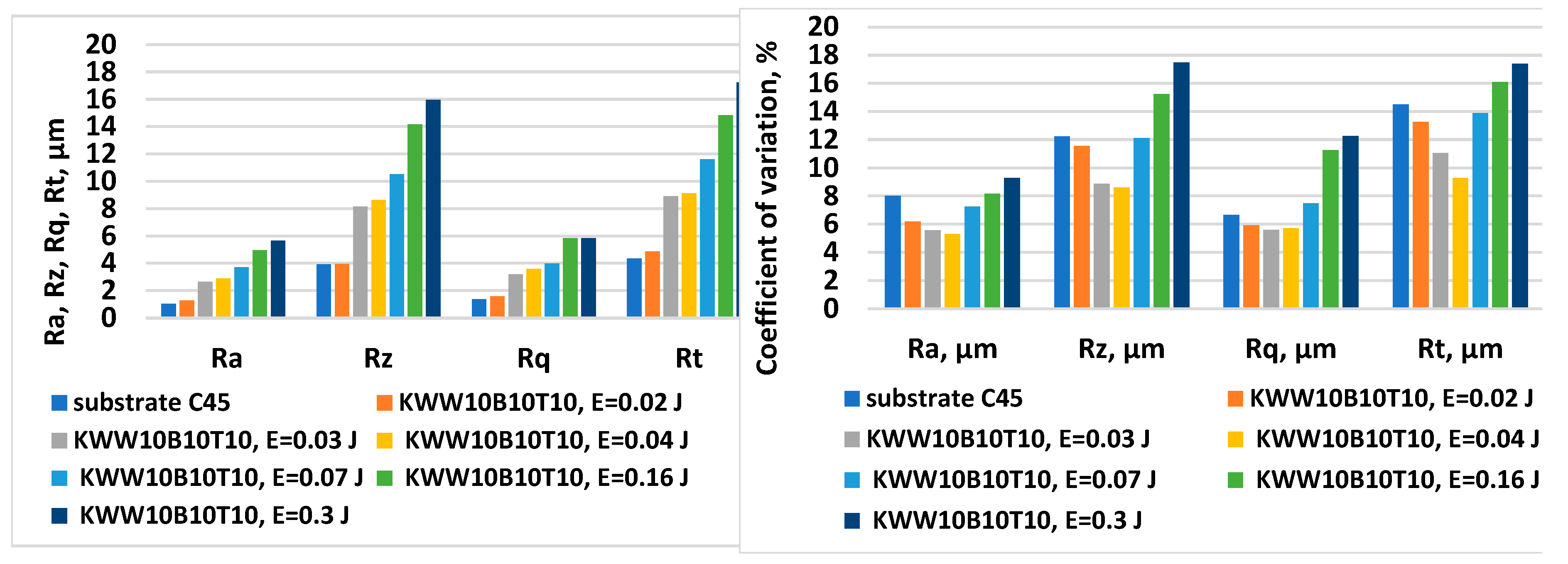
Figure 2.
Variation of the roughness Ra of the electrode coated with KWW10B10T20 as a function of the pulse energy.
Figure 2.
Variation of the roughness Ra of the electrode coated with KWW10B10T20 as a function of the pulse energy.
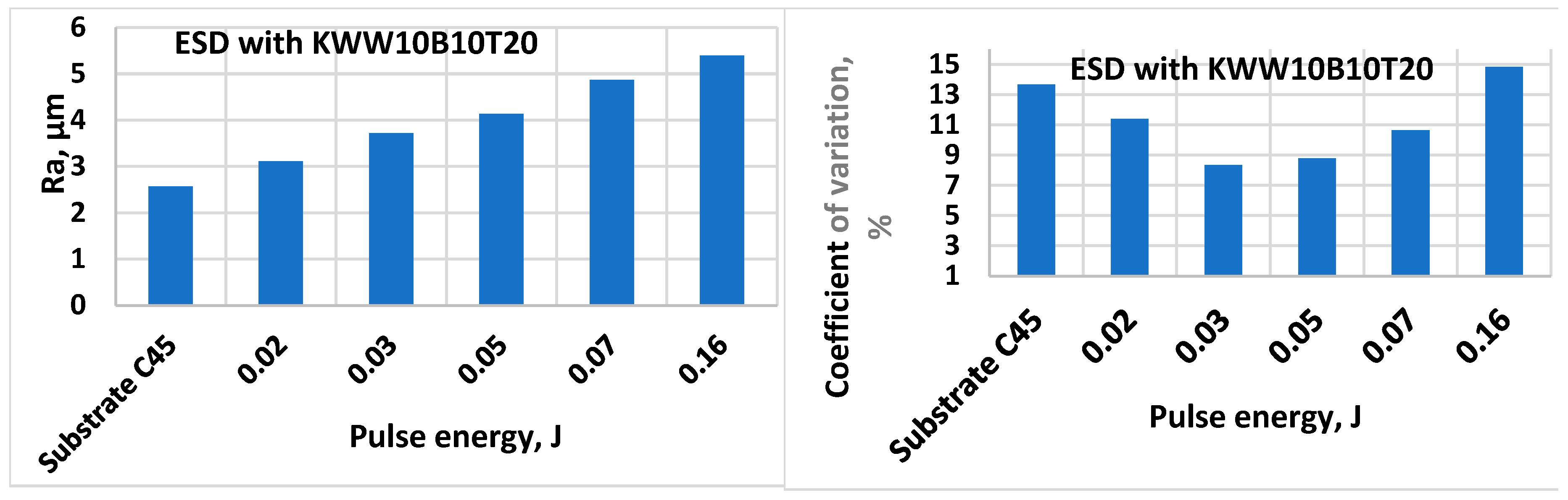
Figure 3.
Photographs of the topography and surface relief of KWW10B10T10 and KWB10T10 coatings deposited on C45 steel at low and high pulse energy.
Figure 3.
Photographs of the topography and surface relief of KWW10B10T10 and KWB10T10 coatings deposited on C45 steel at low and high pulse energy.
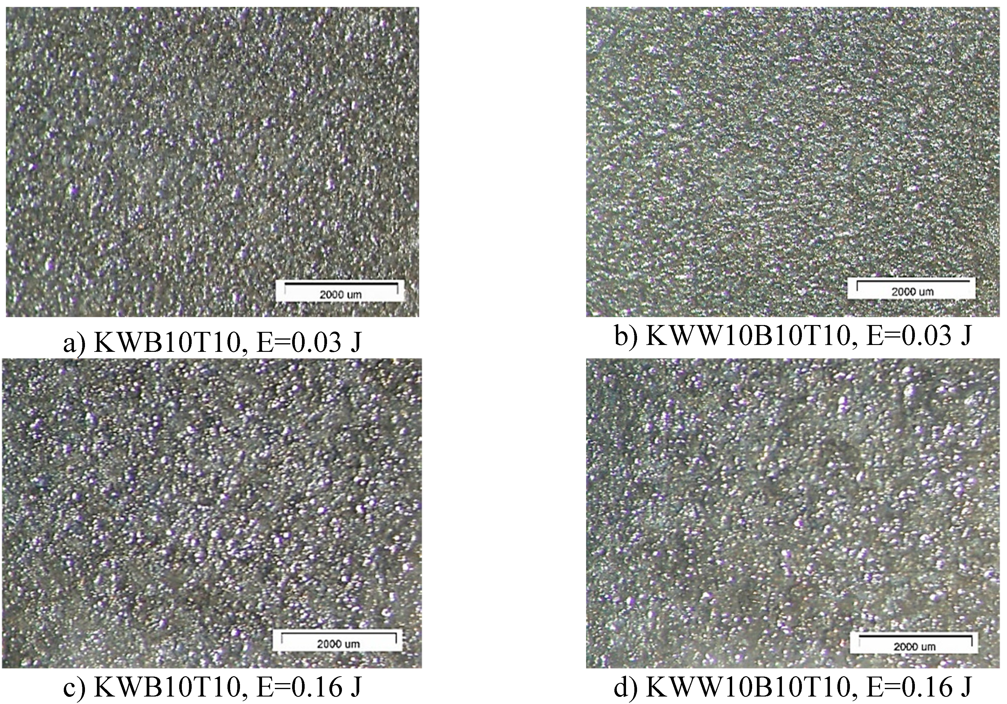
Figure 4.
Photographs of the topography and surface relief of KWW10B10T20 and KWB10T20 coatings deposited on C45 steel at low and high pulse energy.
Figure 4.
Photographs of the topography and surface relief of KWW10B10T20 and KWB10T20 coatings deposited on C45 steel at low and high pulse energy.
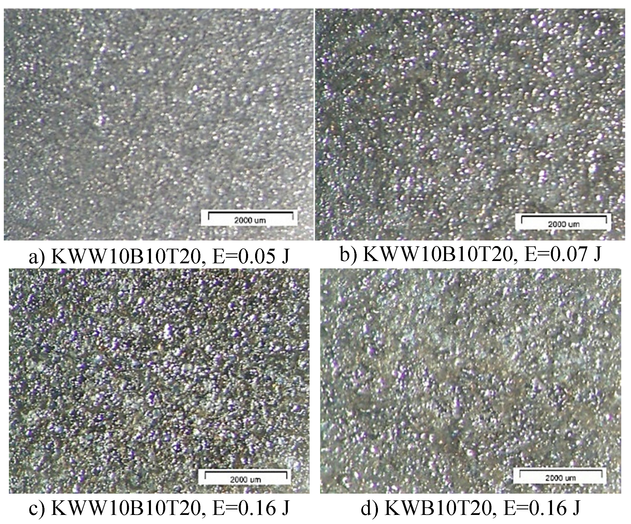
Figure 5.
Photographs of the topography and surface relief of KWW10B20T20 and KWB20T20 coatings deposited on C45 steel at low and high pulse energy.
Figure 5.
Photographs of the topography and surface relief of KWW10B20T20 and KWB20T20 coatings deposited on C45 steel at low and high pulse energy.
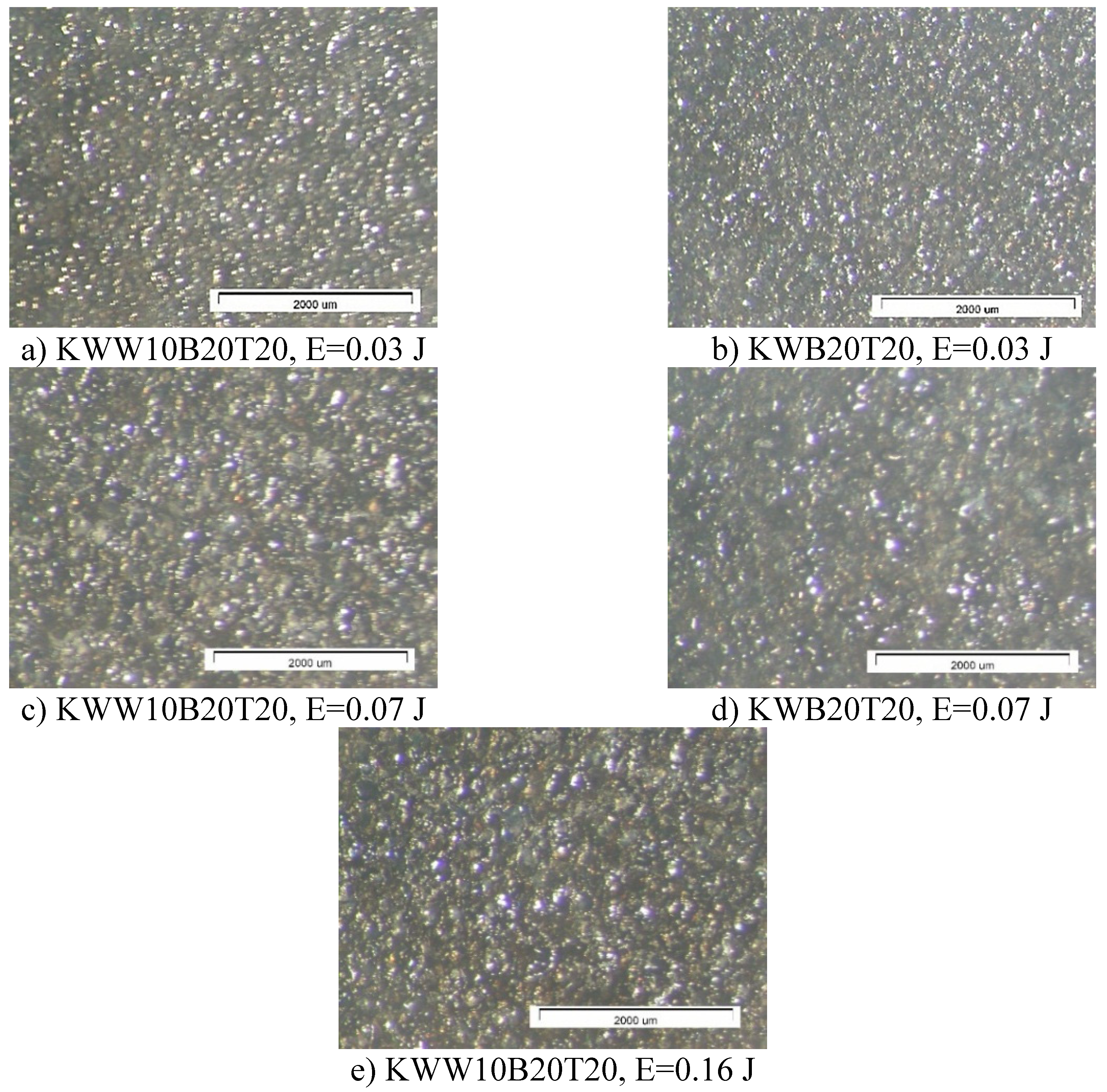
Figure 6.
SEM images of coatings from KWW10B10T10 and KWW10B10T20 electrodes deposited on steel 45 at different pulse energies.
Figure 6.
SEM images of coatings from KWW10B10T10 and KWW10B10T20 electrodes deposited on steel 45 at different pulse energies.
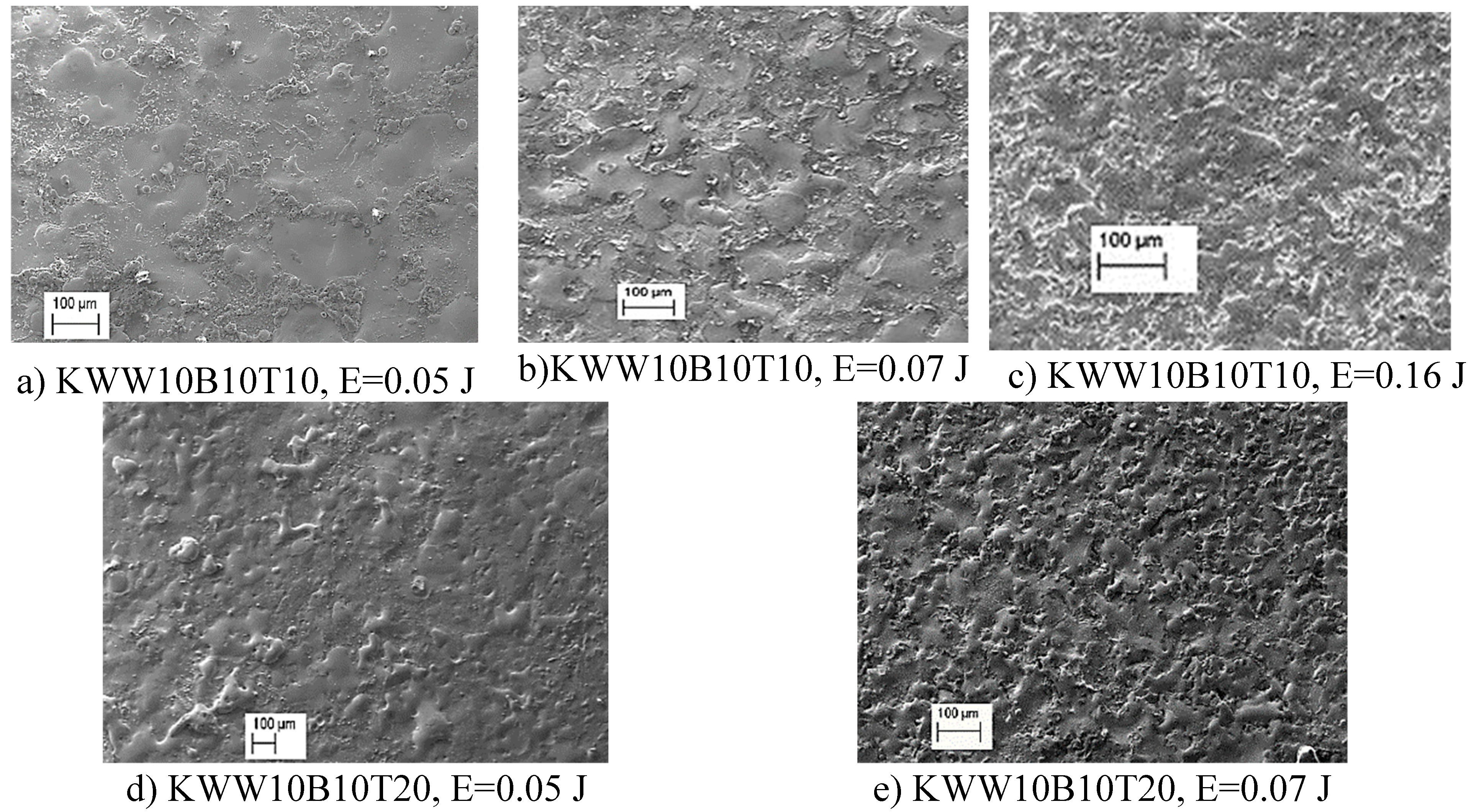
Figure 7.
SEM images at different magnifications of coatings from the studied electrodes deposited on steel 45.
Figure 7.
SEM images at different magnifications of coatings from the studied electrodes deposited on steel 45.
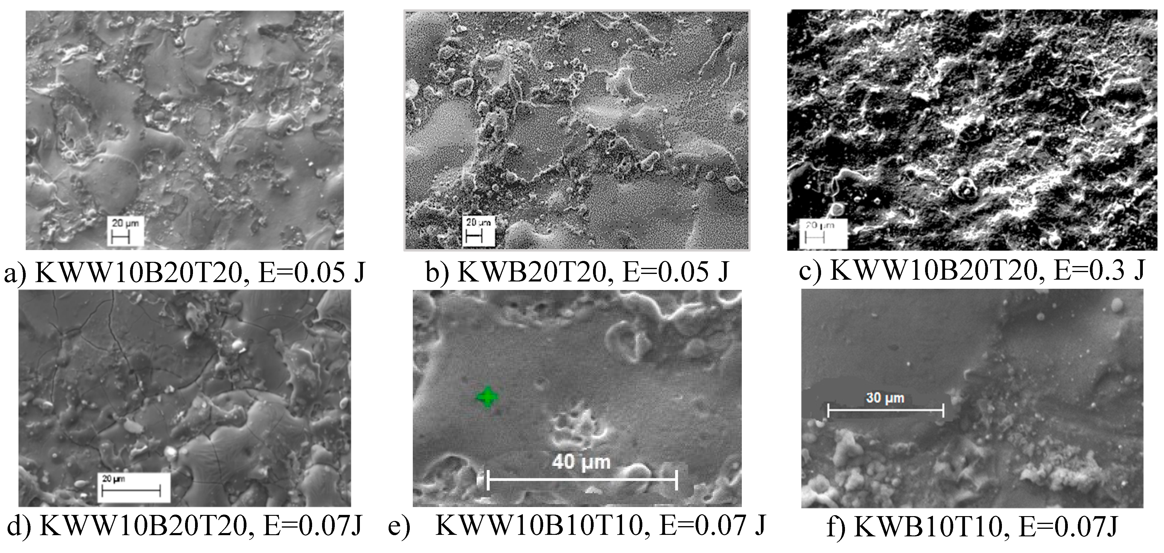
Figure 8.
Cross-section of coatings from KWW10B10T10 (a), KWW10B10T20 (b,c) and KWW10B20T20 (d) electrodes deposited at pulse energy E=0.07 J.
Figure 8.
Cross-section of coatings from KWW10B10T10 (a), KWW10B10T20 (b,c) and KWW10B20T20 (d) electrodes deposited at pulse energy E=0.07 J.
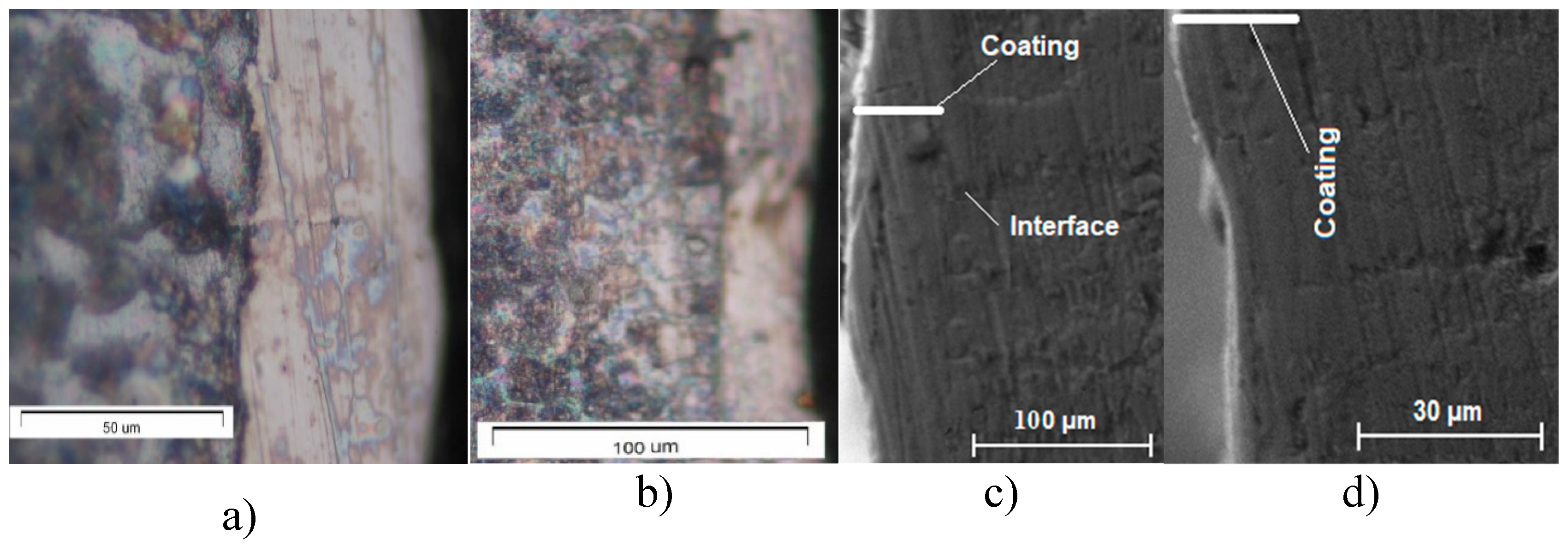
Figure 9.
XRD diffraction patterns of coatings from electrodes at different pulse energy.
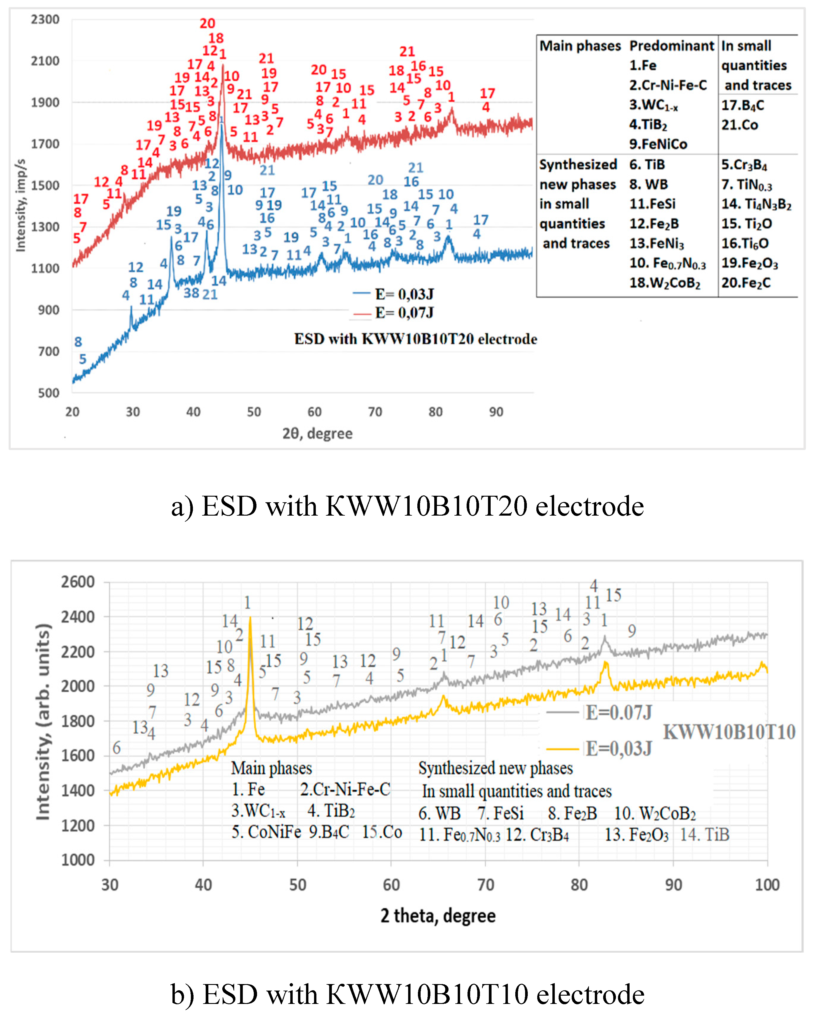
Figure 10.
XRD diffraction patterns of coatings from electrodes at pulse energy 0.05 J.
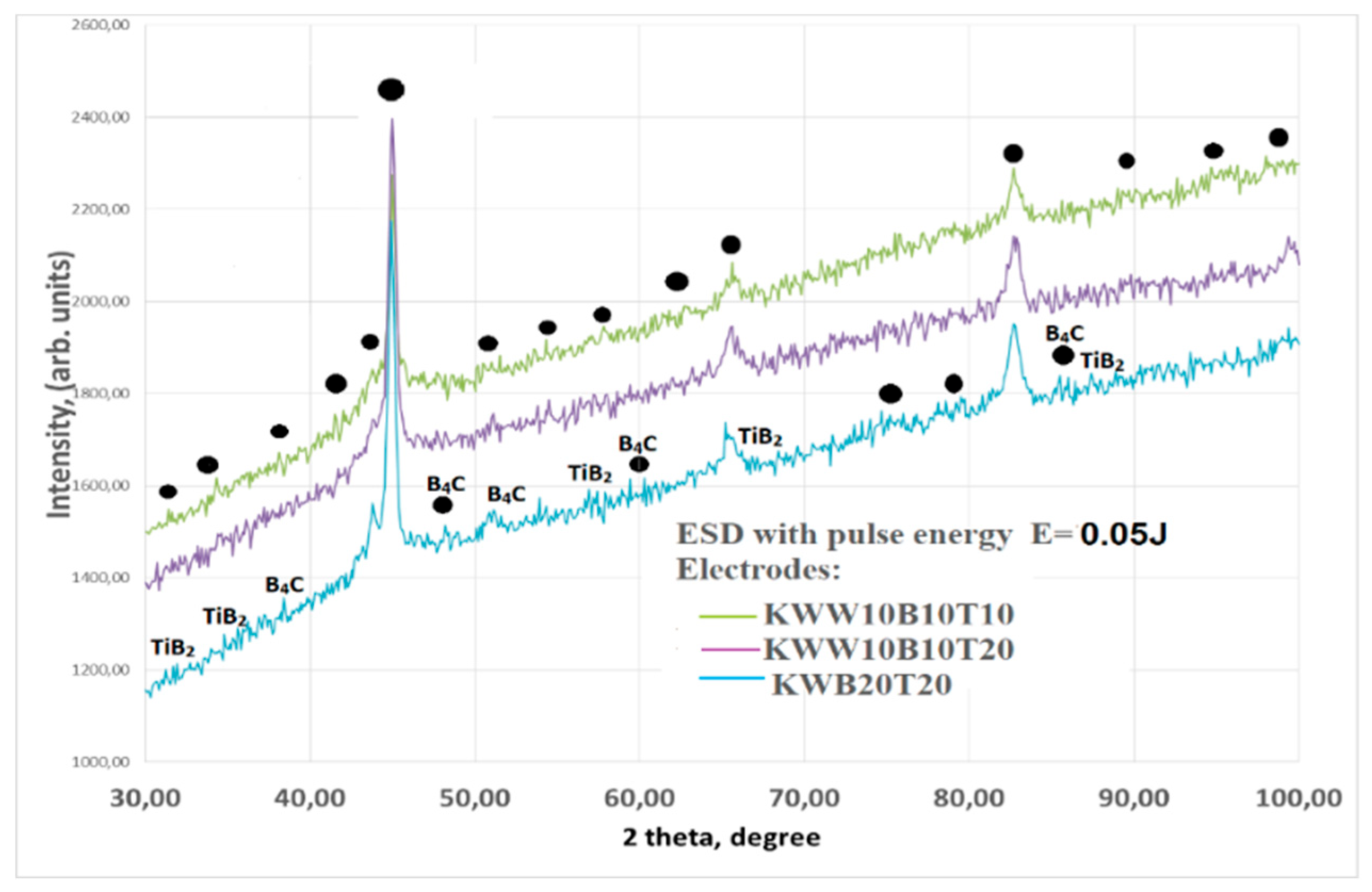
Figure 11.
EDX spectrum of coatings from KWW10B10T10, KWW10B10T20 and KWW10B10T20 electrodes.
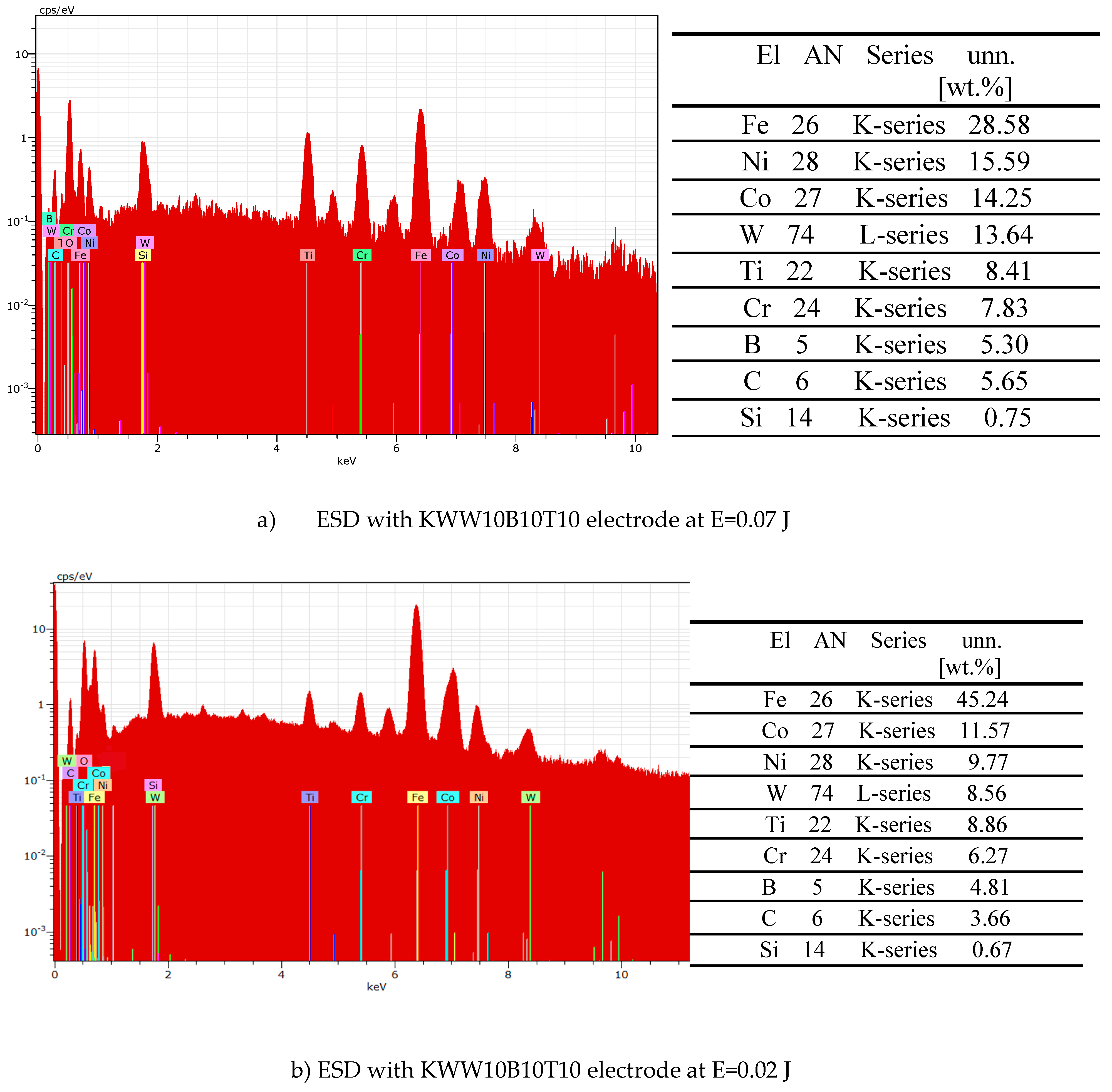
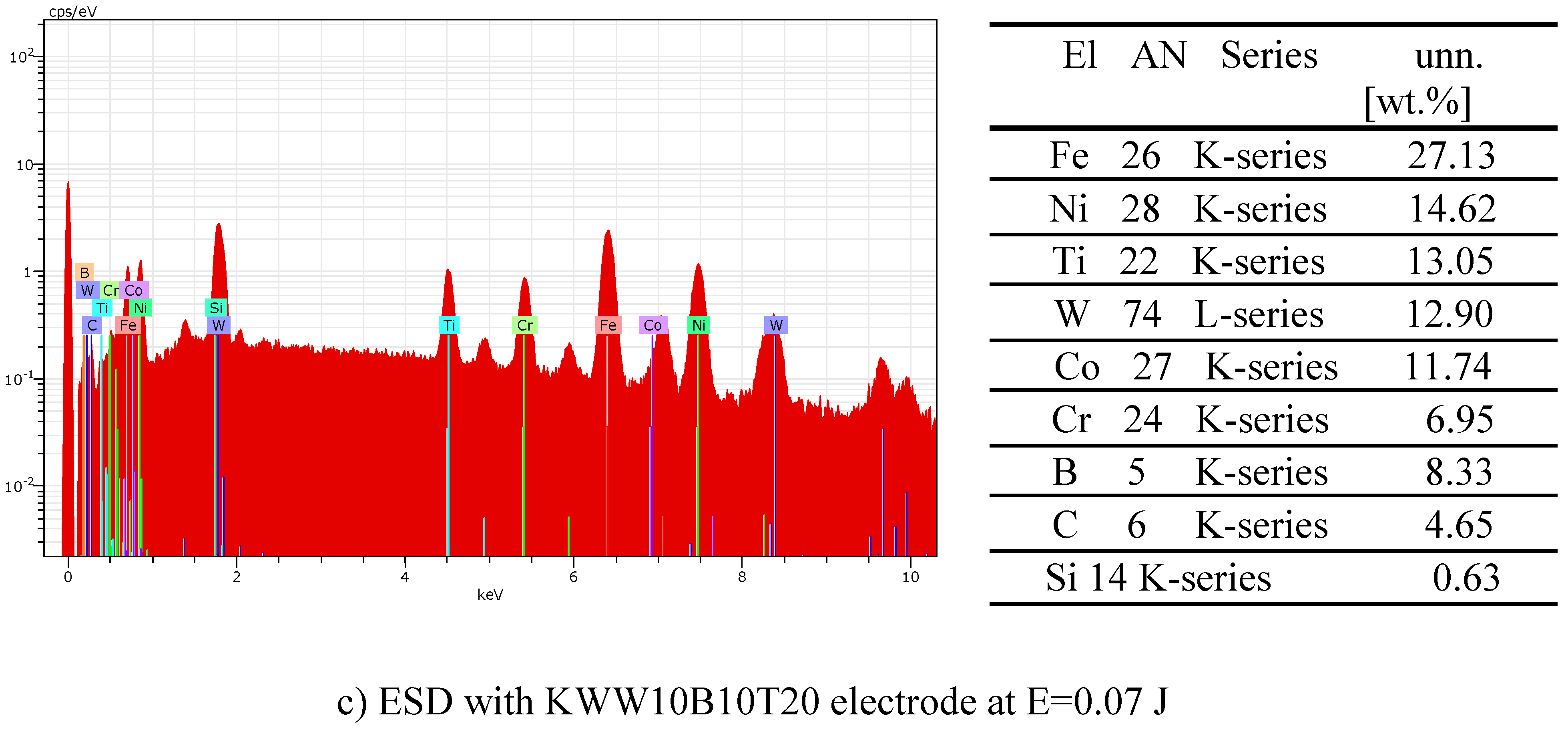
Figure 12.
COF, Tangential Force, Scrach traces and Acoustic Emission of ESD Coatings at E=0.07 J versus the Normal Force.
Figure 12.
COF, Tangential Force, Scrach traces and Acoustic Emission of ESD Coatings at E=0.07 J versus the Normal Force.
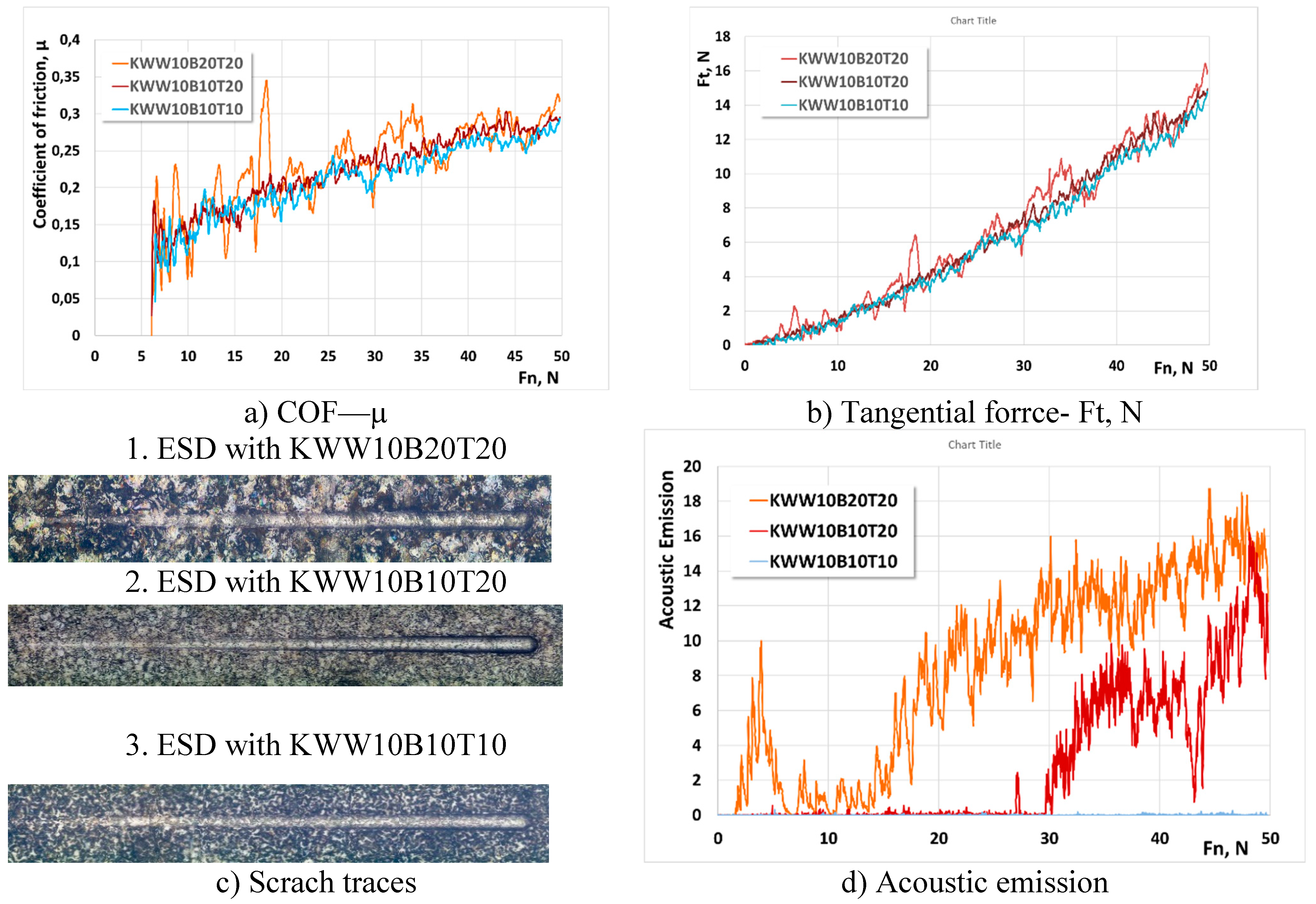
Figure 13.
Mass loss(a) and wear rate(b) of coatings from KWW10B10T10 electrode as a function of friction path and pulse energy at a load of 10 N.
Figure 13.
Mass loss(a) and wear rate(b) of coatings from KWW10B10T10 electrode as a function of friction path and pulse energy at a load of 10 N.
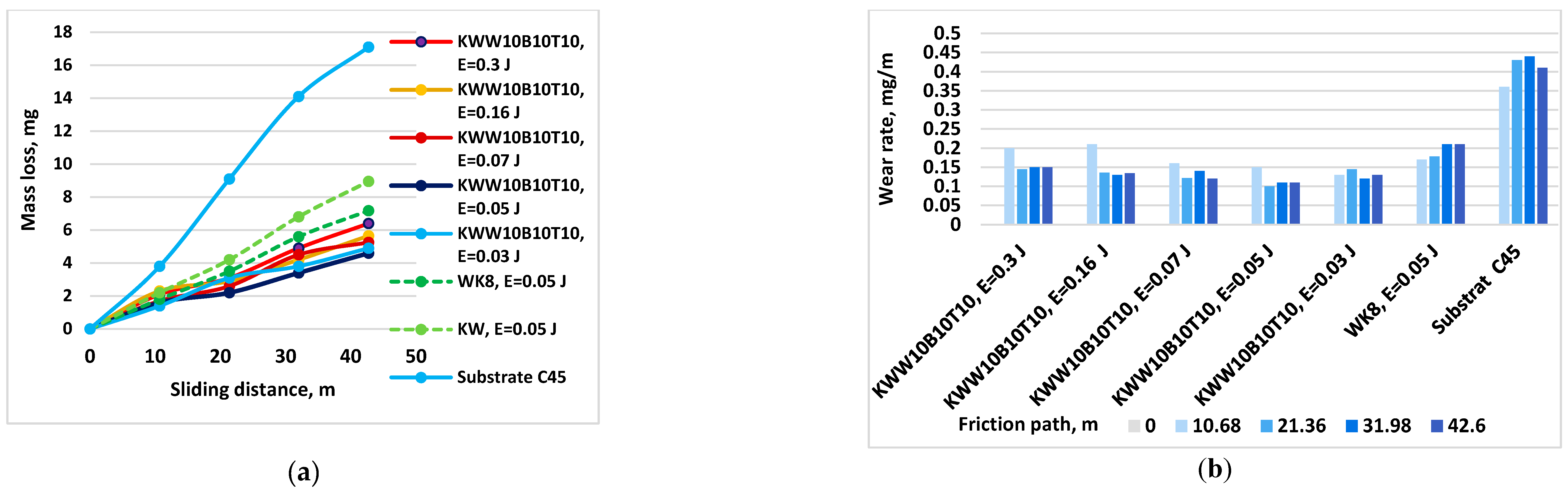
Figure 14.
Mass loss (a) and wear rate(b) of coatings from “KW”” and “”KWW” electrodes as a function of friction path and pulse energy at a load of 10N.
Figure 14.
Mass loss (a) and wear rate(b) of coatings from “KW”” and “”KWW” electrodes as a function of friction path and pulse energy at a load of 10N.
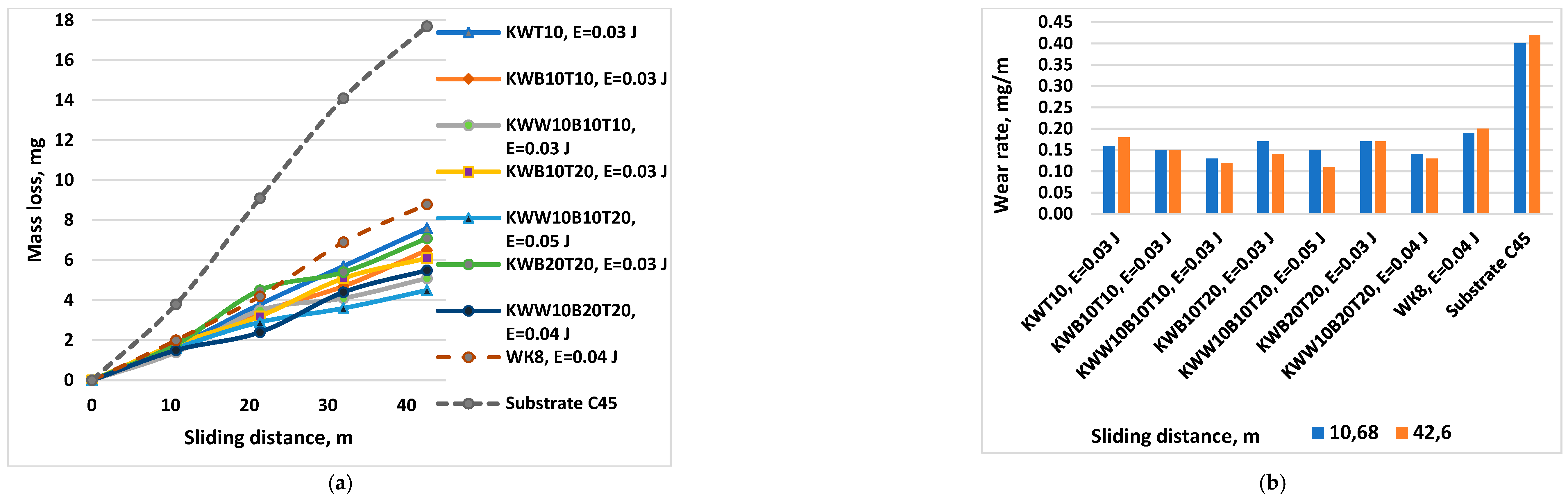
Figure 15.
Mass loss (a)and wear rate(b)of coatings from KW and KWW electrodes as a function of friction path and pulse energy at a load of 5 N.
Figure 15.
Mass loss (a)and wear rate(b)of coatings from KW and KWW electrodes as a function of friction path and pulse energy at a load of 5 N.
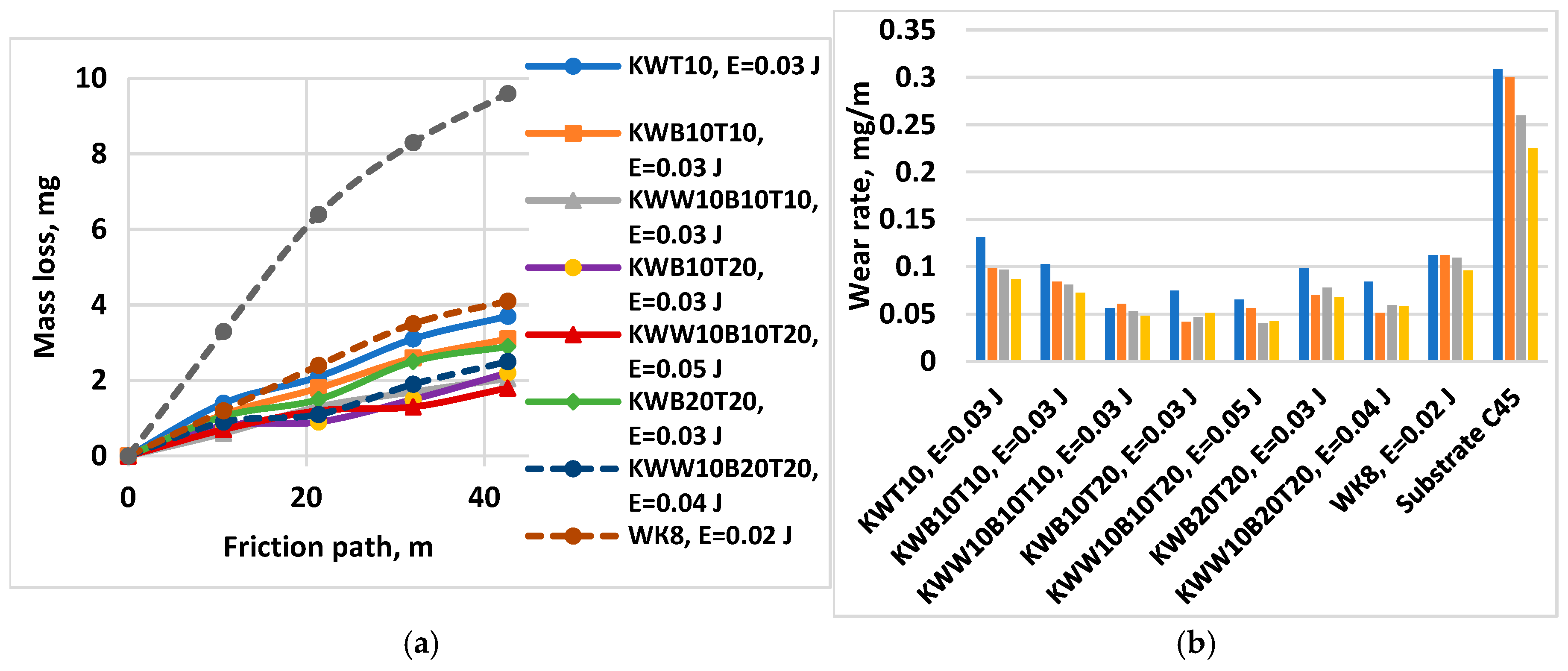

Table 1.
Chemical composition of the bonding powder mixtures. .
| Element , % | С | Si | Cr | Fe | B | Co | Ni | Designation of composition |
|---|---|---|---|---|---|---|---|---|
| CoNiCrBSi | 1.5 | 1.5 | 23 | 0.5 | 1.5 | 40 | balance | KW=45%CoNiCrBSi + 55%WC |
Table 2.
Composition and designation of multicomponent electrode materials for ESD.
| Designation/ Composition, % | KW | WC- Сo8 | TiB2 | B4C |
|---|---|---|---|---|
| KWT10 | 90 | - | 10 | - |
| KWB10T10 | 80 | - | 10 | 10 |
| KWW10B10T10 | 70 | 10 | 10 | 10 |
| KWB10T20 | 70 | - | 20 | 10 |
| KWW10B10T20 | 50 | 10 | 20 | 20 |
| KWB20T20 | 60 | - | 20 | 20 |
| KWW10B20T20 | 50 | 10 | 20 | 20 |
| WК8 | 92/8 |
Table 3.
Used ESD Modes with Vibrating Electrode.
| № of regimes | 1 | 2 | 3 | 4 | 5 | 6 |
|---|---|---|---|---|---|---|
| Сapacity, С, µF | 5 | 10 | 15 | 20 | 50 | 100 |
| Pulse energy Е, J | 0.02 | 0.03 | ≈0.05 | ≈0.07 | ≈0.16 | ≈0.3J |
Table 5.
Parameters of coatings obtained with ESD with vibrating apparatus.
| № | Electrode, Е= 0.03÷0.3 J | Ra, mm | d, mm | Hv, GPa | Coeff. Of hardening |
|---|---|---|---|---|---|
| 1 | WК8 | 1.8÷5.5 | 14÷42 | 7.8÷12 | 3÷5 |
| 2 | KWТ10 | 2.5÷5.3 | 19÷66 | 8÷12 | 3÷5 |
| 3 | KWB10T10 | 2.5÷5.3 | 18÷63 | 8.3÷12.5 | 3÷5.3 |
| 4 | KWW10B10T10 | 2.3÷5.6 | 16÷59 | 8.8÷13 | 3.5÷5.6 |
| 5 | KWB10T20 | 2.2÷5.5 | 16÷56 | 8.8÷13 | 3.5÷5.6 |
| 6 | KWW10B10Т20 | 2.2÷5.9 | 20÷53 | 9.5÷14.5 | 3.6÷6.2 |
| 7 | KWB20T20 | 2.1÷5.8 | 18÷55 | 9÷14 | 3.8÷6 |
| 8 | KWW10B20T20 | 2.1÷6.8 | 18÷55 | 9.5÷15 | 3.8÷6.4 |
Table 6.
Roughness, thickness and growth of the cathode in ESD with vibrating apparatus.
| Electrode, Impulse energy, J | Roughness and thickness δ of the coating after 3 electrode passes | Average thickness | Cathode growth, mg/cm2 | |||||
|---|---|---|---|---|---|---|---|---|
| Roughness, µm | Thickness δ, µm | µm | mg/cm2 | |||||
| Ra | Rz | Rt | min | max | ||||
| Substrate | 2.38 | 9.56 | 2.7 | 9.65 | - | - | - | - |
| KWW10B20T20,Е=0.07 | 4.84 | 14.12 | 5.50 | 17.63 | 27.6 | 35.5 | 30 | 0.67 |
| KWB20T20, Е=0.07 | 4.46 | 12.72 | 5.16 | 15.58 | 30.2 | 38.1 | 33 | 0.83 |
| KWW10B10T10, E0.07 | 4.29 | 12.62 | 4.67 | 14.63 | 33.6 | 41.9 | 36 | 1.2 |
| KWW10B10T10, E0.05 | 4.04 | 11.8 | 4.44 | 13.48 | 23.7 | 30.3 | 28 | 0.88 |
| KWB10T10, E=0.07 | 3.87 | 12.2 | 3.6 | 14.11 | 35.6 | 43.5 | 40 | 1.43 |
| KWB10T10, E=0.05 | 3.38 | 9.56 | 3.7 | 11.65 | 26.5 | 35.9 | 32 | 1.05 |
Disclaimer/Publisher’s Note: The statements, opinions and data contained in all publications are solely those of the individual author(s) and contributor(s) and not of MDPI and/or the editor(s). MDPI and/or the editor(s) disclaim responsibility for any injury to people or property resulting from any ideas, methods, instructions or products referred to in the content. |
© 2025 by the authors. Licensee MDPI, Basel, Switzerland. This article is an open access article distributed under the terms and conditions of the Creative Commons Attribution (CC BY) license (http://creativecommons.org/licenses/by/4.0/).
Copyright: This open access article is published under a Creative Commons CC BY 4.0 license, which permit the free download, distribution, and reuse, provided that the author and preprint are cited in any reuse.


