
Submitted:
03 April 2025
Posted:
04 April 2025
You are already at the latest version
Abstract
Silicon modulators play a crucial role in optical communication systems. Over the past thirty years, there has been a notable enhancement in the bandwidth of silicon modulators; however, their operational speed remains constrained by the resistance-capacitance (RC) time constant. This study presents a silicon strip waveguide-based modulator configured in a series push-pull (SPP) arrangement, which effectively mitigates the limitations imposed by the RC time factor. The modulator exhibits a flat electro-optic (EO) response extending up to 68 GHz. Additionally, it achieves a phase shift of 0.022 radians for a C-band optical wave when subjected to a 15 GHz radio-frequency (RF) modulation signal with an amplitude of 2.45 V.
Keywords:
capacitive coupling
; bandwidth enhancement
; silicon modulators
; series push-pull configuration
1. Introduction
Integrated modulators are key components in modern optical communication systems, especially in short-reach optical communication systems [1,2,3]. Silicon-on-insulator (SOI) based integrated modulators are attractive for their CMOS (complementary metal-oxide semiconductor) compatibility, high bandwidth, and low insertion loss. Among the different types of silicon modulators, the depletion type silicon modulator is the most popular in the field of optical communications because of its high-speed operation. In most cases the depletion type silicon modulator consists of a rib waveguide with a lightly doped lateral PN diode in the core region and metal electrodes placed on the highly doped silicon slabs on either side of the waveguide core region. For high-speed operation such modulators are operated in the reverse bias regime [4]. The bandwidth of these modulators are limited to ∼40 GHz because of the RC time constant which comes from the highly doped silicon slabs [5]. Although the bandwidth of silicon modulators has been enhanced using travelling wave electrodes (TWE) [6], segmented TWEs [7], and slow light effects [8], very few approaches have been made to get rid of the RC time limitation. In our previous reports, we have demonstrated a novel approach to enhance the bandwidth by coupling the electrical signal to the waveguide core capacitively. We also demonstrated a silicon strip waveguide-based silicon modulator or a capacitively coupled silicon (CC-Si) Mach-Zehnder interferometer (MZI) modulator in single drive configuration [9,10,11].
In this paper, we present a CC-Si MZI modulator configured in a series push-pull (SPP) arrangement, which was fabricated in a multi-project wafer (MPW) run at the Advanced Micro Foundry (AMF). The EO characterization of the modulator reveals the capability to generate sidebands reaching frequencies of up to 68 GHz around a continuous wave (CW) optical carrier in the C-band, with a flat EO response observed across this frequency range. Notably, for an RF modulation signal of 15 GHz, a linear correlation was established between the phase shift of the C-band optical carrier and the amplitude of the RF modulation signal. Specifically, the phase shift of the optical signal was observed to increase from 0.014 radians to 0.022 radians in a linear manner as the RF signal amplitude was elevated from 1.35 V to 2.45 V.
2. Device Structure
The CC-Si modulator was fabricated on a standard SOI wafer with a 220 nm thick silicon device layer () on a 2 m thick buried oxide (BOX) layer () and 725 m thick silicon substrate (). Figure 1(a) shows the cross-sectional view of the modulator in the SPP configuration. Each arm of the MZI consists of a 650 nm wide () silicon strip waveguide to ensure single mode operation for the fundamental transverse electric (TE) optical mode. The lightly doped PN junction is in the center of the waveguide. A highly P-doped (P++) silicon slab and a highly N-doped (N++) silicon slab with a thickness () of 90 nm thickness () are placed 500 nm away from the P side and the N side of the waveguide respectively. There are two aluminum metal layers (Mt1 and Mt2) used for DC (direct current) bias and RF transmission lines. There are two aluminum vias (Via1 and Via2) which establish electrical connections between the highly doped silicon slab layer and the Mt1 layers and between the Mt1 and the Mt2 layers respectively. All layers are covered with a ∼3 m () silicon dioxide upper cladding. The bond pad opening layer exposes the Mt2 layer at the contact pad area for external DC and RF electrical connections. To enhance the electric field inside the waveguide the Mt1 layer of the DC contact is extended above the strip waveguide and the Via1 layer of the signal and ground contacts are pushed away from the waveguide sufficiently to avoid electrical field confinement between two Mt1 layers. Lumerical Device was used to perform electrostatic simulations by applying different DC bias voltage, between –3V and -30V maintaining the signal terminal voltage, = 0 V. For these simulations, we considered Mt1 layer thickness, = 50 nm, Mt2 layer thickness, = 100 nm, Via-1 layer thickness, = 750 nm, and Via-2 layer thickness, = 2 m. We also considered the P, N, P++ and N++ doping concentrations to be ∼3.5 ×, ∼5 ×, ∼1.8 ×, and ∼8.7 × respectively. Figure 1(b) & Figure 1(c) show the electron concentrations and Figure 1(d) & Figure 1(e) show the hole concentrations in the waveguide region of the left arm of the MZI for the abovementioned respectively. We notice a change of carrier concentrations when is reduced from -3 V to -30 V. As a result, we get a change of effective refractive index, . An estimation of has been calculated in [9,11]. We use this change in effective index, combined with an asymmetric bias between the two signal and ground electrodes to produce the push-pull modulator. The RF modulation signal is applied between the signal and the ground contacts of the device. A negative DC bias is applied at the central electrical contact. For fast operation, the PN diode in both arms of the MZI must be at reverse bias all the time. Therefore, the magnitude of the DC bias voltage must be at least equal to the amplitude of the RF signal. This is how a differential push-pull operation is achieved by an MZI modulator in SPP configuration.
3. Experimental Demonstration
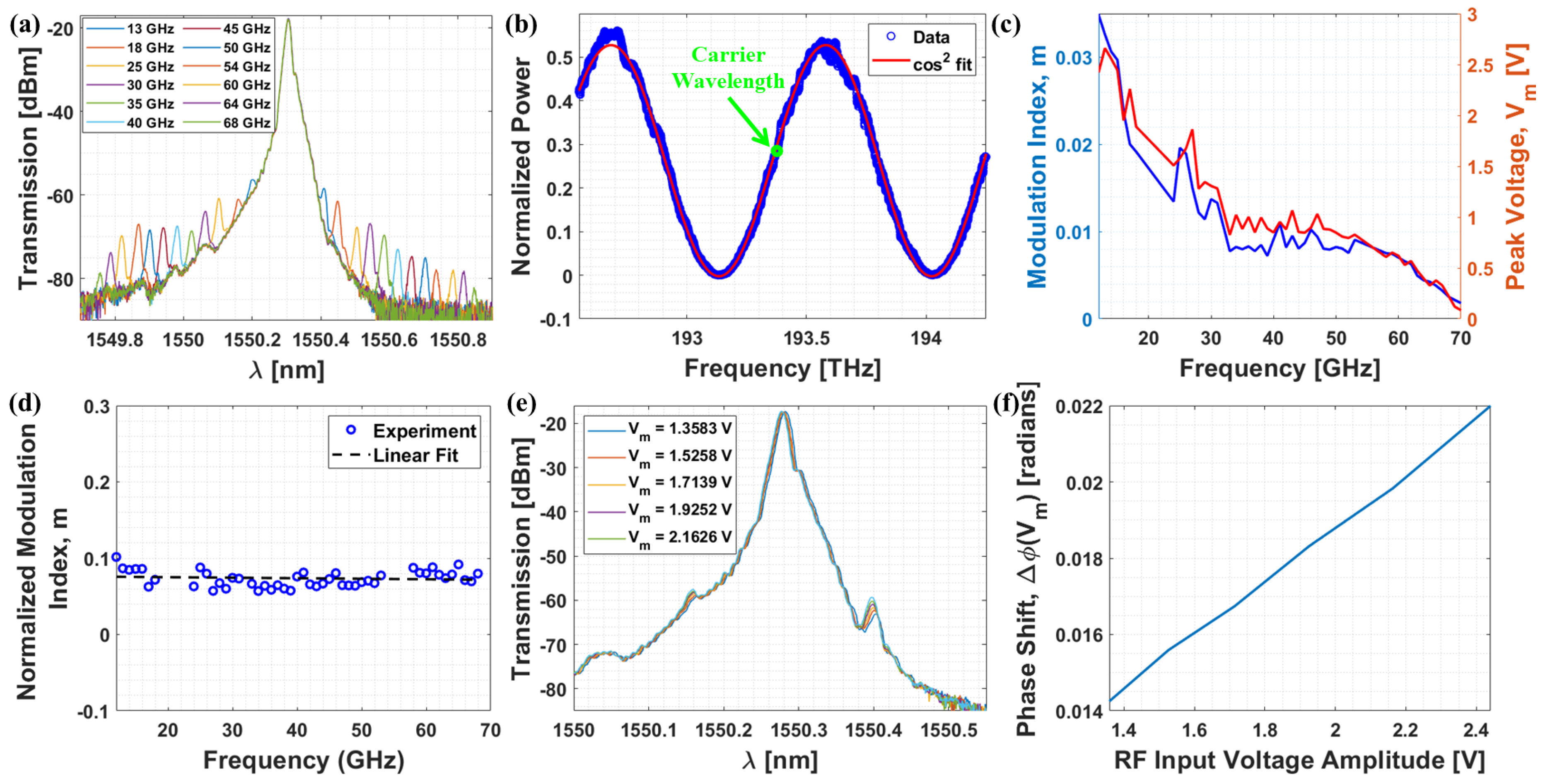
To demonstrate the EO response of the CC-Si MZI modulator in SPP configuration we built an experimental setup in Figure 1(f). A high-power RF signal generator which can generate sinusoidal signal up to 70 GHz with +25 dBm power was used. The RF signals are applied between the signal and ground terminal of the MZI. A 50 Ω termination load is used to terminate the other end of the RF transmission line of the modulator. A negative DC bias should be applied to the DC bias contact, however, the RF signal generator is very sensitive to the DC voltages and therefore, for the safety of the instrument we avoid applying any DC bias. We use a tunable laser source (TLS) to generate a +9 dBm CW optical carrier at 1550.31 nm wavelength which is near the quadrature point of the MZI. The optical carrier is coupled to the chip using a grating coupler after passing through a polarization controller (PC). The coupled optical carrier signal is split into two MZI arms using a 1×2 multimode interference (MMI) coupler. After phase modulation optical signals from both arms are combined using a 2×2 MMI coupler. These modulated optical signals are coupled out of the chip using two other grating couplers. One of the modulated signals is detected by a high-resolution optical spectrum analyzer (OSA). In this way, we can generate sidebands up to 68 GHz, which can be seen from Figure 2(a). The frequency dependent modulation indices, is calculated from the carrier-sideband power ratio expressed by Eq. 1 [12].
Here, and (=) are the optical carrier frequency and frequency of the modulation RF signals respectively. ϕ is the constant phase difference between two arms of the unbalanced MZI. and are the Bessel functions of first kind for orders 0 and 1 respectively. Carrier nulling is difficult to achieve in this case due to the distortions of the function of an unbalanced MZI CC-Si modulator and noise. To reduce the relevant uncertainties, the normalized transmission spectrum of the unbalanced MZI modulator is measured over a wider spectral range that includes the current operating optical carrier. In order to estimate the exact phase shift, ϕ, a fit of a model function of an unbalanced MZI modulator shown in Eq. 2 is performed with the experimental data.
In Eq. 2, , , and where, is the path length difference between the two arms of the MZI, and , and are the propagation constant, the first and the second order derivatives of the propagation constant respectively. is the center frequency of the frequency range of the unbalanced MZI spectrum. The fitting parameters , , , , and are determined using the least-square fit method. The phase shift, ϕ of an unbalanced CC-Si MZI modulator can be calculated from Eq. 3.
After eliminating the effect of the grating couplers, the measured transmission spectrum is shown by the blue circles in Figure 2(b). The fit to the measured data using Eq. 2 is shown by the red line in Figure 2(b) and the operating optical carrier is pointed out with a green circle in Figure 2(b). The phase shift value, ϕ, and the carrier to sideband ratio, are used to calculate the using Eq. 1, the blue line of Figure 2(c). The signal generator can generate a power of +25 dBm for all frequencies. However, the losses of the RF probes and the RF cable are frequency dependent. Hence, the RF power which is actually applied at the modulator terminal is microwave frequency dependent. We measure the RF power for different frequencies using an RF power meter. The associated frequency dependent peak voltages, based on these RF power measurements are plotted in the red line of Figure 2(c). It is observed that the curve of follow the curve of . Later, the curve is normalized with respect to a frequency independent +2 dBm RF power which is plotted in Figure 2(d). A liner fit of the normalized is also shown in Figure 2(d) which shows that the the CC-Si MZI modulator has a very flat frequency response.
Followed by the EO measurement, we measure transmission spectra of different modulated optical signals for 15 GHz RF sinusoidal signals with different powers i.e., different peak voltage, . The measured transmission spectra are shown in Figure 2(e). Before applying the 15 GHz RF signals, we measure the powers of different RF signals using an RF power meter. Thus, we determine the phase shift, ϕ for 15 GHz RF-signal which is voltage dependent. Figure 2(f) shows the phase shifts for different RF powers i.e., different of 15 GHz signals. We observe a linear relationship between between and ϕ. increase from 0.014 radians to 0.022 radians almost linearly as the amplitude of the 15 GHz RF signal was raised from 1.35 V to 2.45 V. These devices are expected to have comparatively lower phase shifts, since we use silicon dioxide cladding with low dielectric constant that reduces the electrical field confinement within the waveguide region [9].
4. Conclusions
To summarize, we have demonstrated a CC-Si modulator which can enhance the bandwidth of silicon devices by eliminating the RC time limitation. Lumerical Device simulations were performed to show the working principle of the CC-Si modulator. We performed the EO measurement of a CC-Si MZI modulator in SPP configuration and observe a flat EO frequency response up to 68 GHz which proves the broadband nature of this device. 15 GHz RF modulation signals with different amplitudes were used to calculate the voltage dependent phase shift, ϕ. We observed almost linear relationship between the phase shift of a C-band optical carrier and the amplitude of the RF modulation signal. The phase shift of the optical signal increased from 0.014 radians to 0.022 radians almost linearly while the RF signal amplitude was elevated from 1.35 V to 2.45 V.
The EO response of the CC-Si modulator clearly shows that it will be flat beyond 68 GHz. We are currently limited by the RF power and the maximum frequency provided by the signal generator. The of this modulator is high due to the low dielectric constant silicon dioxide ( = 3.9) cladding [13] around a comparatively higher dielectric constant silicon ( = 11.9) waveguide [14] which results in more electrical field drop outside of the waveguide core. This limitation can be improved by replacing the silicon dioxide cladding with a very high dielectric constant material like barium titanate which has been found effective in different platforms like silicon-organic hybrid (SOH) platform [15,16,17,18] and lithium niobate-on insulator (LNOI) platform [19,20,21]. However, deposition of a high dielectric constant material is not a standard for existing silicon photonic foundries. But we are currently investigating this approach by doing back-end-of-line (BEOL) post-fabrication processes. Moreover, due to the resolution of the OSA we chose a sideband at comparatively higher frequency (15 GHz) of RF signal where different other factors such as impedance mismatch, microwave propagation loss, velocity mismatch between the optical and the RF mode play a significant role. Thus, the voltage dependent phase shift, ϕ in such high frequency will be much lower compared to the phase shift values measured at kHz range frequencies. Also, for the safety of the signal generator no DC bias is applied which leads to higher chirping by generating positive in both MZI arms. As a result, the differential phase shift between two arms is smaller than the phase shift with a negative DC bias. Thus, the absence of negative DC bias leads to lower phase shifts. Additionally, without any DC bias for half-cycle of an RF modulation sinusoidal signal the PN diode will be in forward bias which can potentially limit the bandwidth of the device. Nevertheless, with progress in characterization and fabrication techniques we believe that these challenges can be solved which will allow high-performance devices.
Funding
This work is supported by the Natural Sciences and Engineering Research Council of Canada (NSERC) discovery grant (RGPIN-2022-04871), and by CMC Microsystems.
Data Availability Statement
The data sets generated and/or analyzed during the current study are available from the corresponding authors on reasonable request.
Acknowledgments
We express our gratitude to Prof. Joyce Poon for her assistance in characterizing the device. We also thank Prof. George Eleftheriades & Alex MacKay for use of the high-power signal generator and the RF power meter, and Prof. Li Qian & Alexander Greenwood for access to the high-resolution optical spectrum analyzer.
Conflicts of Interest
The authors declare no conflict of interest.
Abbreviations
The following abbreviations are used in this manuscript:
| RC | Resistance-capacitance |
| SPP | Series push-pull |
| RF | Radio-frequency |
| CMOS | Complementary metal-oxide semiconductor |
| TWE | Traveling wave electrode |
| CC-Si | Capacitively coupled silicon |
| MZI | Mach-Zehnder interferometer |
| MPW | Multi-project wafer |
| AMF | Advanced Micro Foundry |
| EO | Electro-optic |
| CW | Continuous wave |
| PN | P-type/N-Type |
| DC | Direct current |
| TLS | Tunable laser source |
| PC | Polarization controller |
| MMI | Multimode interference |
| OSA | Optical spectrum analyzer |
| LNOI | Lithium niobate on insulator |
| BEOL | Back-end-of-line |
References
- Dong, P.; Lee, J.; Chen, Y.K.; Buhl, L.L.; Chandrasekhar, S.; Sinsky, J.H.; Kim, K. Four-channel 100-Gb/s per channel discrete multi-tone modulation using silicon photonic integrated circuits. In Proceedings of the 2015 Optical Fiber Communications Conference and Exhibition (OFC); 2015; pp. 1–3. [Google Scholar] [CrossRef]
- Xie, C.; Magill, P.; Li, D.; Zhang, Y.; Zheng, L.; Wang, A.; Bao, Y.; Sui, C.; Streshinsky, M.; Mu, J.; et al. Real-Time Demonstration of Silicon-Photonics-Based QSFP-DD 400GBASE-DR4 Transceivers for Datacenter Applications. In Proceedings of the 2020 Optical Fiber Communications Conference and Exhibition (OFC); 2020; pp. 1–3. [Google Scholar] [CrossRef]
- Yu, H.; Patel, D.; Liu, W.; Malinge, Y.; Doussiere, P.; Lin, W.; Gupta, S.; Narayanan, K.; Hoshino, I.; Bresnehan, M.; et al. 800 Gbps Fully Integrated Silicon Photonics Transmitter for Data Center Applications. In Proceedings of the 2022 Optical Fiber Communications Conference and Exhibition (OFC); 2022; pp. 1–3. [Google Scholar] [CrossRef]
- Liao, L.; Liu, A.; Rubin, D.; Basak, J.; Chetrit, Y.; Nguyen, H.; Cohen, R.; Izhaky, N.; Paniccia, M. 40 Gbit/s silicon optical modulator for high-speed applications. Electronics Letters 2007, 43, 1196–1197. [Google Scholar] [CrossRef]
- Watts, M.R.; Zortman, W.A.; Trotter, D.C.; Young, R.W.; Lentine, A.L. Low-Voltage, Compact, Depletion-Mode, Silicon Mach–Zehnder Modulator. IEEE Journal of Selected Topics in Quantum Electronics 2010, 16, 159–164. [Google Scholar] [CrossRef]
- Zhang, H.; Li, M.; Zhang, Y.; Zhang, D.; Liao, Q.; He, J.; Hu, S.; Zhang, B.; Wang, L.; Xiao, X.; et al. 800 Gbit/s transmission over 1 km single-mode fiber using a four-channel silicon photonic transmitter. Photon. Res. 2020, 8, 1776–1782. [Google Scholar] [CrossRef]
- Mohammadi, A.; Zheng, Z.; Lin, J.; Rad, M.M.; Zhang, X.; Rusch, L.A.; Shi, W. Segmented Silicon Photonic Modulator with a 67-GHz Bandwidth for High-Speed Signaling. In Proceedings of the Optical Fiber Communication Conference (OFC) 2022. Optica Publishing Group; 2022; p. Th3C.1. [Google Scholar] [CrossRef]
- Han, C.; Zheng, Z.; Shu, H.; Jin, M.; Qin, J.; Chen, R.; Tao, Y.; Shen, B.; Bai, B.; Yang, F.; et al. Slow-light silicon modulator with 110-GHz bandwidth. Science Advances 2023, 9, eadi5339. [Google Scholar] [CrossRef] [PubMed]
- Alam, A.S.; Sun, H.; Masnad, M.; Alamgir, I.; na, J.A.; Aitchison, J.S. Carrier Dispersion Modulation in a Silicon Strip Waveguide. In Proceedings of the CLEO 2024. Optica Publishing Group; 2024; p. JTh2A.195. [Google Scholar] [CrossRef]
- Alam, A.S.; Sun, H.; Masnad, M.M.; Alamgir, I.; Azaña, J.; Aitchison, J.S. Bandwidth Estimation of a Silicon Strip Waveguide Based Optical Modulator. In Proceedings of the Frontiers in Optics + Laser Science 2024 (FiO, LS). Optica Publishing Group; 2024; p. JW4A.50. [Google Scholar] [CrossRef]
- Alam, A.S.; Aitchison, J.S. Capacitively Coupled Silicon Modulator Fabricated on the Standard Silicon-on-Insulator Platform. IEEE Photonics Journal 2025. [Google Scholar] [CrossRef]
- Shi, Y.; Yan, L.; Willner, A. High-speed electrooptic modulator characterization using optical spectrum analysis. Journal of Lightwave Technology 2003, 21, 2358–2367. [Google Scholar] [CrossRef]
- Reynard, J.; Verove, C.; Sabouret, E.; Motte, P.; Descouts, B.; Chaton, C.; Michailos, J.; Barla, K. Integration of fluorine-doped silicon oxide in copper pilot line for 0.12-μm technology. Microelectronic Engineering 2002, 60, 113–118. [Google Scholar] [CrossRef]
- Alfaraj, N.; Lin, C.C.C.; Nasif, S.; Rajput, S.; Helmy, A.S. Facile integration of electro-optic SiO2/ITO heterointerfaces in MIS structures for CMOS-compatible plasmonic waveguide modulation. Light: Advanced Manufacturing 2023, 4, 420. [Google Scholar] [CrossRef]
- Alam, A.S. Design, Fabrication and Characterization of Capacitively Coupled Silicon-Organic Hybrid Modulators. Master’s Thesis, Karlsruhe Institute of Technology (KIT), 2017. [Google Scholar] [CrossRef]
- Ummethala, S.; Kemal, J.N.; Lauermann, M.; Alam, A.S.; Zwickel, H.; Harter, T.; Kutuvantavida, Y.; Hahn, L.; Nandam, S.H.; Elder, D.L.; et al. Capacitively Coupled Silicon-Organic Hybrid Modulator for 200 Gbit/s PAM-4 Signaling. In Proceedings of the Conference on Lasers and Electro-Optics. Optica Publishing Group; 2019; p. JTh5B.2. [Google Scholar] [CrossRef]
- Ummethala, S.; Kemal, J.N.; Alam, A.S.; Lauermann, M.; Kuzmin, A.; Kutuvantavida, Y.; Nandam, S.H.; Hahn, L.; Elder, D.L.; Dalton, L.R.; et al. Hybrid electro-optic modulator combining silicon photonic slot waveguides with high-k radio-frequency slotlines. Optica 2021, 8, 511–519. [Google Scholar] [CrossRef]
- Ummethala, S. Plasmonic-Organic and Silicon-Organic Hybrid Modulators for High-Speed Signal Processing. Ph.D. Thesis, 43.32.03; LK 01. Karlsruhe Institute of Technology (KIT), 2021. [Google Scholar] [CrossRef]
- Alam, A.S.; Aitchison, J.S. Low Half-Wave-Voltage Lithium Niobate Modulator Using High-K Dielectric Material Cladding. In Proceedings of the Optica Advanced Photonics Congress 2022. Optica Publishing Group; 2022; p. JTu2A.9. [Google Scholar] [CrossRef]
- Alam, A.S.; Aitchison, J.S. Optimization of a Broadband Lithium Niobate-Barium Titanate Hybrid Modulator With Low Half-Wave-Voltage-Length Product. IEEE Photonics Journal 2023, 15, 1–7. [Google Scholar] [CrossRef]
- Chen, N.; Lou, K.; Yu, Y.; He, X.; Chu, T. High-Efficiency Electro-Optic Modulator on Thin-Film Lithium Niobate with High-Permittivity Cladding. Laser & Photonics Reviews 2023, 17, 2200927. [Google Scholar] [CrossRef]
Figure 1.
(a) Cross-sectional view of a CC-Si MZI modulator in SPP configuration. Lumerical Device simulations for the electron concentrations for of (b) -3 V & (c) -30 V respectively and for the hole concentrations for of (d) -3 V & (e) -30 V respectively. (f) Experimental setup for EO measurement of the CC-Si MZI modulator in SPP configuration.
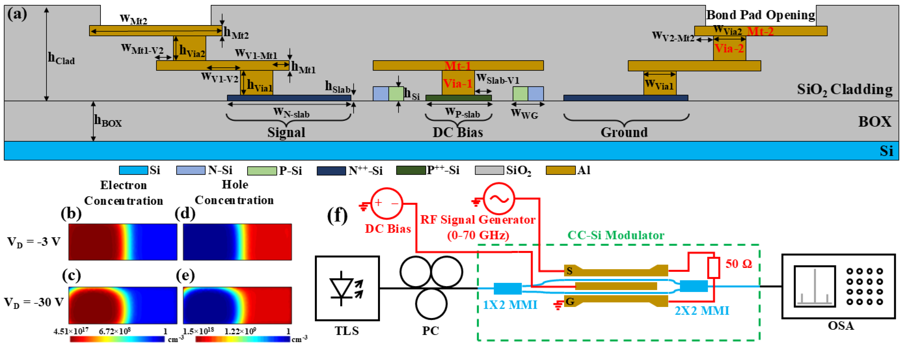
Figure 2.
(a) Transmission spectra of the modulated optical signal for RF signal of different frequencies. (b) Measured intensity spectra of an unbalanced MZI CC-Si modulator (blue circles) in SPP configuration and associated fit (red line) according to Eq. 2. The carrier wavelength is pointed out with a green circle. (c) Frequency dependent (blue line) and associated (red line). (d) Normalized and associated linear fit. (e) Transmission spectra of modulated optical signal for different RF power at 15 GHz. (f) Voltage dependent phase shift, ϕ at 15 GHz.
Disclaimer/Publisher’s Note: The statements, opinions and data contained in all publications are solely those of the individual author(s) and contributor(s) and not of MDPI and/or the editor(s). MDPI and/or the editor(s) disclaim responsibility for any injury to people or property resulting from any ideas, methods, instructions or products referred to in the content. |
© 2025 by the authors. Licensee MDPI, Basel, Switzerland. This article is an open access article distributed under the terms and conditions of the Creative Commons Attribution (CC BY) license (http://creativecommons.org/licenses/by/4.0/).
Copyright: This open access article is published under a Creative Commons CC BY 4.0 license, which permit the free download, distribution, and reuse, provided that the author and preprint are cited in any reuse.


