Submitted:
28 March 2025
Posted:
31 March 2025
You are already at the latest version
Abstract
This paper presents a low-power, wide-tuning range voltage-controlled oscillator (VCO) for C-band applications, fabricated in a TSMC 0.18-μm CMOS process. The proposed VCO achieves a tuning range of 1124 MHz (5.829-4.705 GHz) and a low phase noise of -117.6 dBc/Hz at 1 MHz offset. By employing body-bias technology and an optimized varactor structure, the design significantly improves tuning capability while reducing power consumption to 3.4 mW at a supply voltage of 0.8V. Compared with conventional designs, this VCO achieves a 10-20% increase in tuning range, along with a 5 dB improvement in phase noise performance, making it a compelling solution for emerging RF front-end applications. The ultra-low power consumption makes it particularly advantageous for battery-powered IoT and edge AI devices, extending device operational time while maintaining RF performance. With its wide tuning range, low phase noise, and ultra-low power consumption, this VCO is an ideal solution for emerging RF and millimeter-wave applications, including 5G transceivers, satellite communications, and ultra-low-power IoT devices.
Keywords:
VCO
; tuning range
; phase noise
; low-power design
; C-band
; body-bias technique
; CMOS RF circuits
; IoT applications
1. Introduction
In modern wireless and optical communication systems, efficient voltage-controlled oscillators (VCOs) play a critical role in signal generation. CMOS VCOs have been widely utilized due to their cost-effectiveness and compatibility with System-on-Chip (SoC) integration. However, achieving a wide tuning range and low power consumption while maintaining low phase noise remains a challenge in traditional designs.
Previous research has extensively investigated the fundamental limitations of phase noise and power efficiency in CMOS VCO designs [1,2,3,4]. Several techniques have been proposed to optimize phase noise performance, including approaches aimed at minimizing flicker noise and enhancing the tuning range [4,5,6,7]. More recent studies have introduced advanced techniques such as switched-biasing and resistive tuning to achieve low-power operation and wide frequency tunability. However, these techniques generally suffer from increased design complexity, limited reduction in power consumption, or constrained frequency tuning ranges. Therefore, designing a VCO that simultaneously achieves ultra-low power consumption, low phase noise, wide tuning range, and simplified circuit architecture remains a significant challenge and warrants further exploration.
This work presents a novel CMOS VCO that employs body-bias technology and an optimized buffer circuit to significantly extend the tuning range and enhance power efficiency. Operating at an ultra-low voltage of 0.8 V, the proposed design demonstrates substantially reduced power consumption compared to conventional designs typically requiring supply voltages of 1.2 V or higher. The design achieves a wide tuning range of 1124 MHz and maintains excellent phase noise performance, making it an attractive solution for 5G, satellite communications, and optical networking applications.
2. VCO Design
2.1. Phase Noise
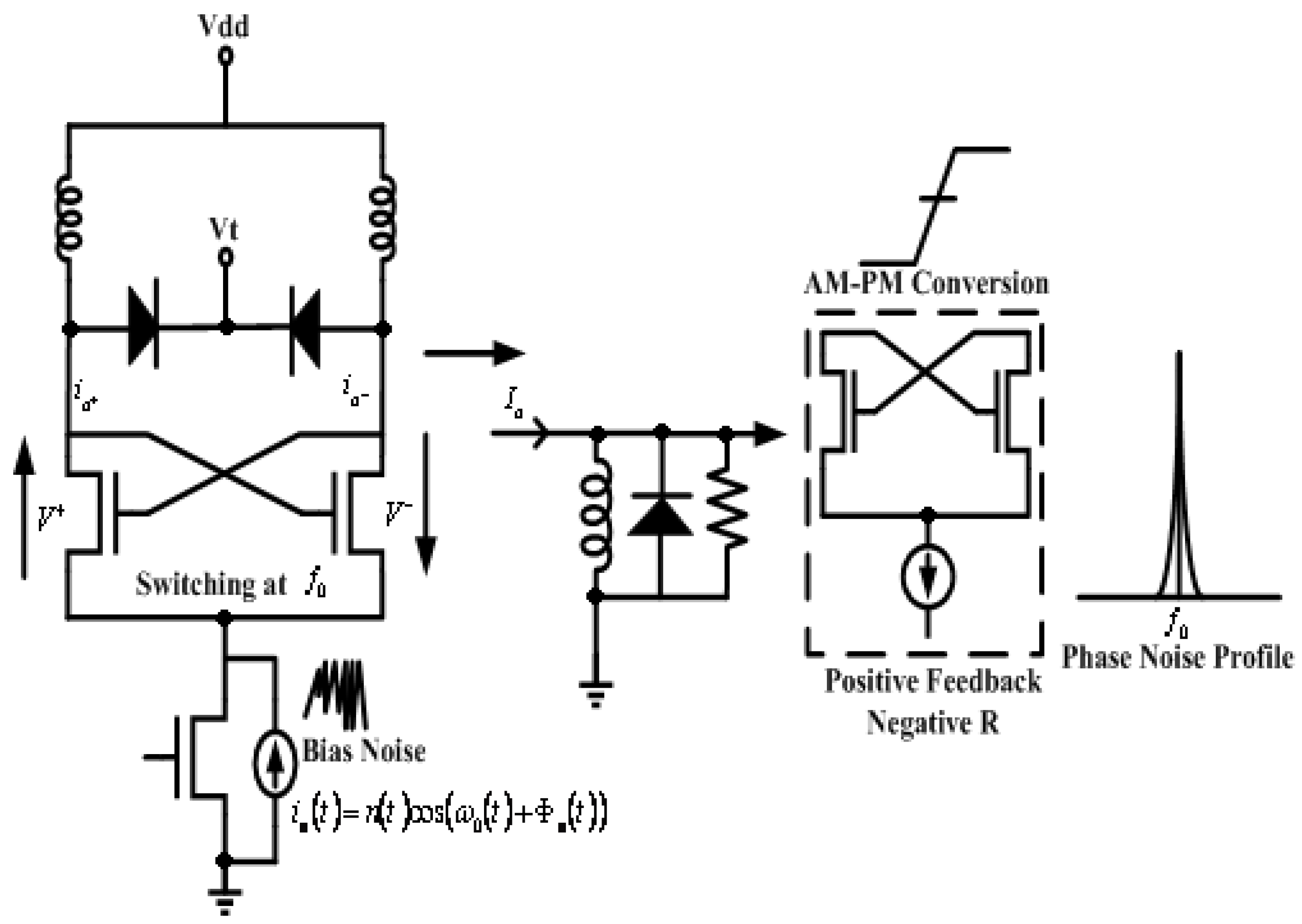
In addition to the noise generated by the circuits, noise from the power supply also affects phase noise [8,9,10]. Using the transistor as the tail current source can decrease the noise from the power supply to the VCO. For PMOS-only VCO, the active region provides the VCO better protection against noise from the power supply [11].
Figure 1.
Conversion of bias noise into phase noise.
That the phase noise improves as quality factor Q increases. The Q of standard inductor L1 is around 8.62, and the Q value of the center tapped inductor L3 is around 5.39. The LC-tank Q is about 7.9, and the impedance at resonance frequency is about 0.75 Ω which is shown in Figure 2.
2.2. VCO Design
The cross-coupled pair is used to suppress parasitic effects introduced by the transistors. It can increase the ratio of tuning capacitance (Cv) and parasitic capacitance (Cparasitic). High Cv/ Cparasitic ratio can achieve a wider frequency tuning range. The PMOS varactor Cv value at different control voltage is shown in Figure 3. Figure 3 shows a good Cmax/Cmin ratio of about 2.78 which can be achieved in a 0.18um bulk CMOS technology with a tuning voltage ± 2V. The oscillator frequency can be determined with Equation (1).
where Cind is the equivalent parallel capacitance of the inductor, Cv is the equivalent capacitance of one varactor, and CMOS is the equivalent parallel capacitance of the NMOS crossed-coupled transistor.
The architecture of the proposed VCO is based on a negative resistance LC-tank oscillator with an NMOS cross-coupled pair (M1 and M2) as the core active components, is shown in Figure 4. The tuning mechanism utilizes a pair of varactors (C1, C2), controlled by the tuning voltage (Vt), enabling frequency adjustment between 5.829 GHz and 4.705 GHz.
To achieve low power consumption, the circuit operates at a reduced supply voltage of 0.8V. A body-biasing technique is applied to transistors M3 and M4, lowering the threshold voltage and enabling operation with minimal power dissipation. This results in a measured power consumption of 3.4 mW. For phase noise optimization, a buffer stage comprising transistors M5, M6, and inductors L3, L4 is included to enhance the output signal swing and minimize phase noise degradation.
Although switched-biasing techniques effectively reduce flicker noise, they typically require additional control circuits, which increase design complexity and power consumption. Instead, our approach utilizes a carefully designed buffer circuit to achieve a comparable improvement in phase noise while maintaining ultra-low power consumption. The measured phase noise at 1 MHz offset is -117.6 dBc/Hz. The buffer circuit also improves waveform symmetry, reducing flicker noise contributions and enhancing overall signal integrity.
3. Simulation and Measurement Results
3.1. Simulation Results
3.2. Measurement Results
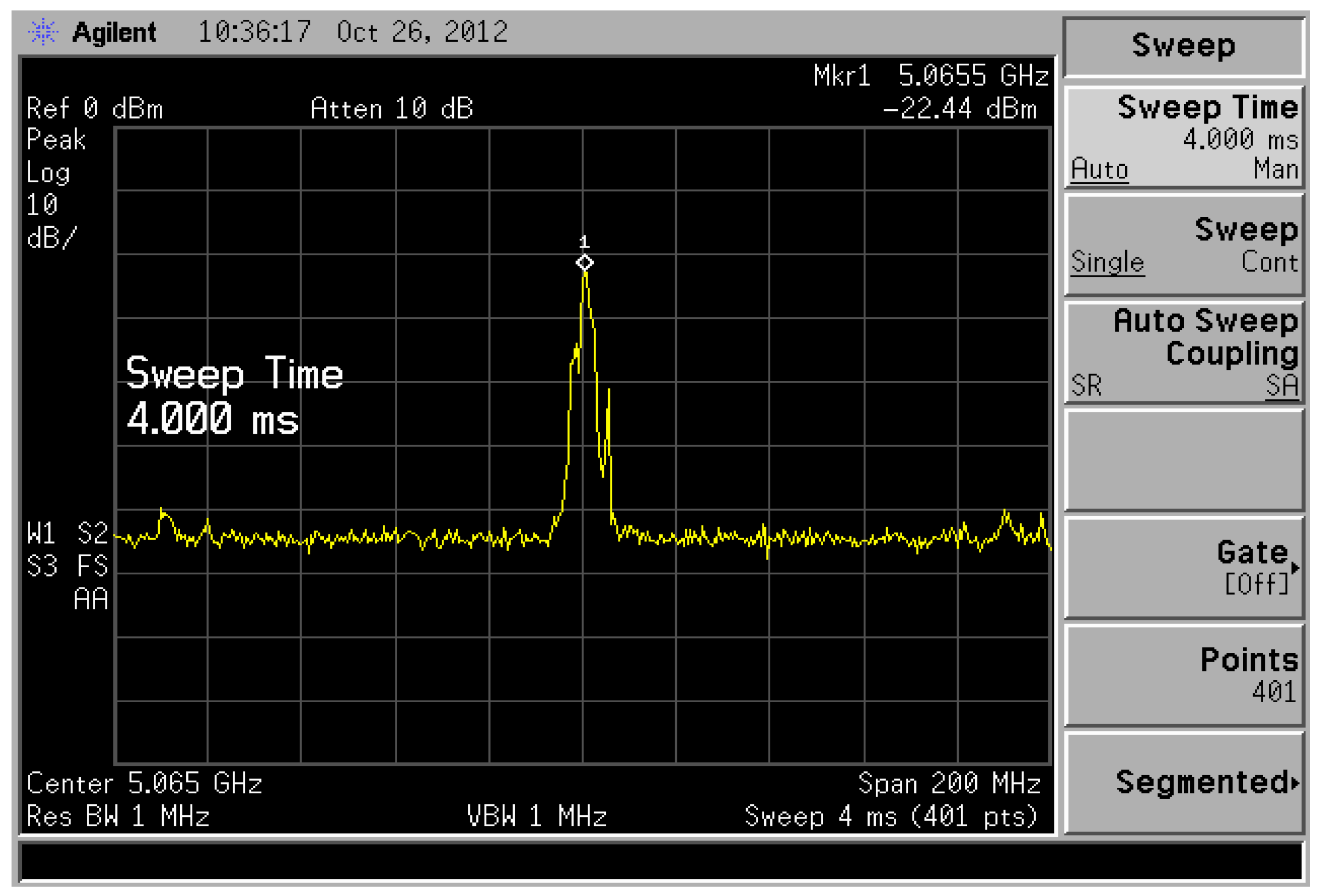
The VCO circuit is designed and fabricated in TSMC’s 0.18-μm CMOS process. The process offers six metal layers for interconnect, and various kinds of RF inductors and varactors. The physical dimensions of the low-phase-noise VCO chip is 0.499 mm2 including pads. The VCO die photo is shown in Figure 7. The measured tuning range is 1124 MHz for control voltage from 0~1.3 V. The VCO exhibits a wide tuning range of 22.2%, as shown in Figure 8. Figure 9 shows the phase noise measurement results. The phase noise at the offset frequencies of 1 MHz is -117.69 dBc/Hz. The frequency spectrum of VCO at 5.06 GHz with power of -22.44 dBm is shown in Figure 10. The FOM value is about -196.6 dBc/Hz and it is calculated using the FOM defined as [12]:
is the oscillation frequency, is the measured phase noise at offset frequency, and PDC is the DC power consumption in mW. The power-frequency-tuning-normalized (PFTN) factor of the proposed VCO is calculated as [13]:
TR is the tuning range and k is Boltzmann’s constant. A temperature of is used for the PFTN calculation.
Table 1 compares the VCO post-simulation and our measured results. Table 2 compares the performance of VCOs based on different CMOS technologies from five previous studies. Most studies use CMOS technology with 0.18 μm, except for [16], which uses 0.13 μm. All designs operate around 5 GHz, with a frequency range of 5.0 to 5.3 GHz. Although our result has slightly worse phase noise performance (-117.7 dBc/Hz) than other studies, it achieves the widest tuning range (22.2%) and the lowest power consumption (3.4 mW) while maintaining a competitive FOM. These characteristics are ideal for low-power wireless communication applications.
Figure 7.
The photograph of the fabricated VCO chip (size: 0.499 mm²).
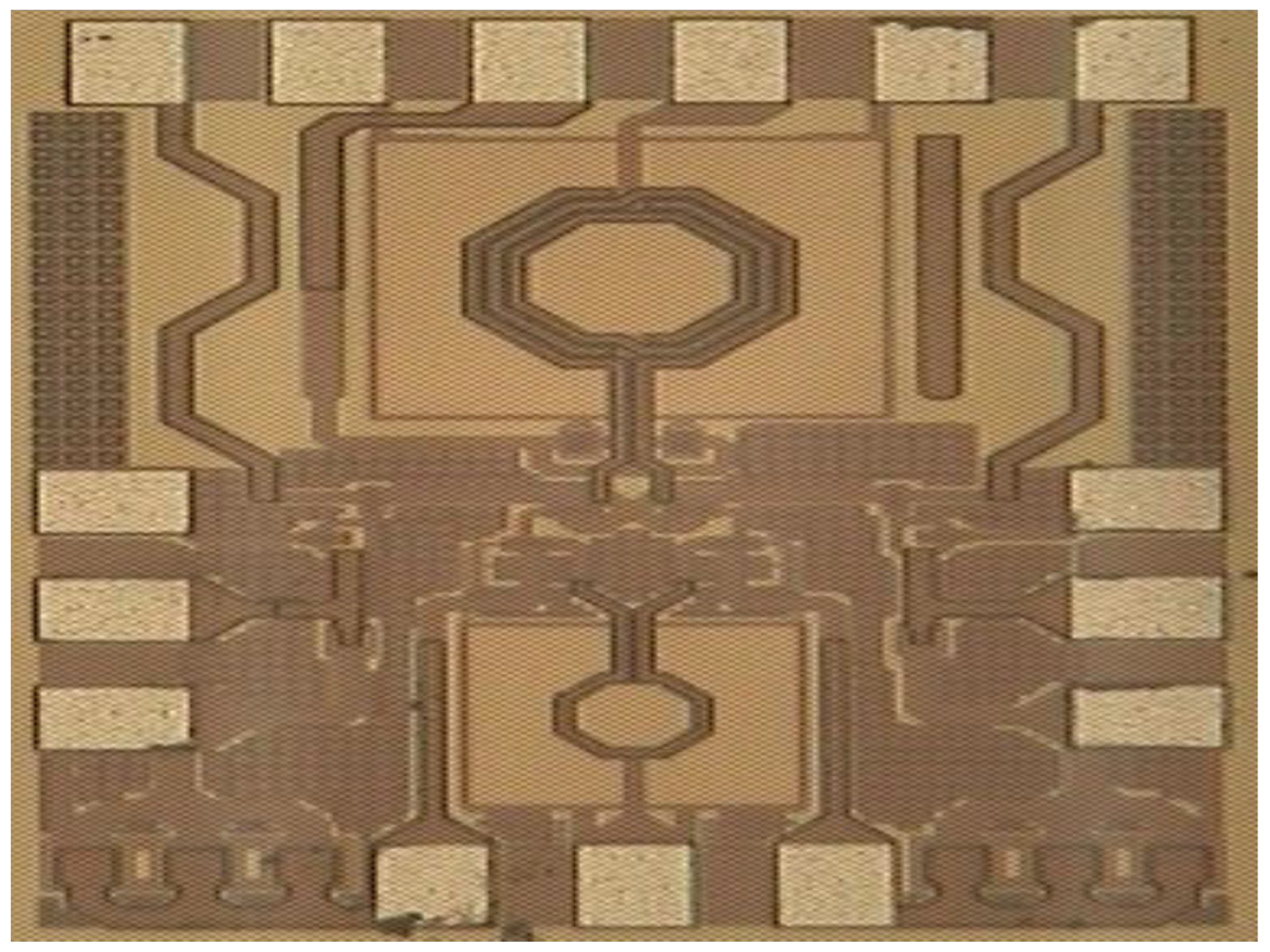
Figure 8.
Measured tuning curve of the VCO.
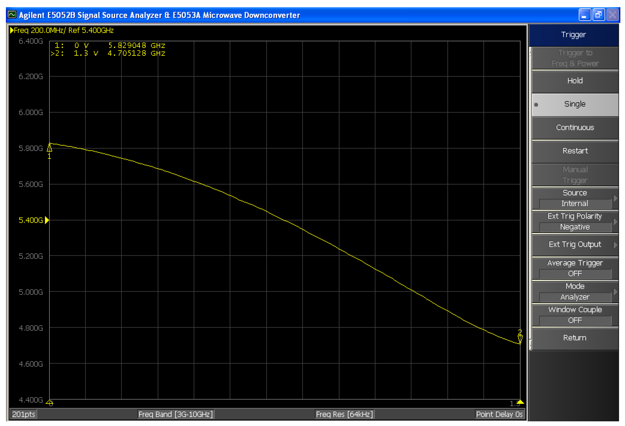
Figure 9.
Measured phase noise at 1 MHz offset showing -117.69 dBc/Hz performance.
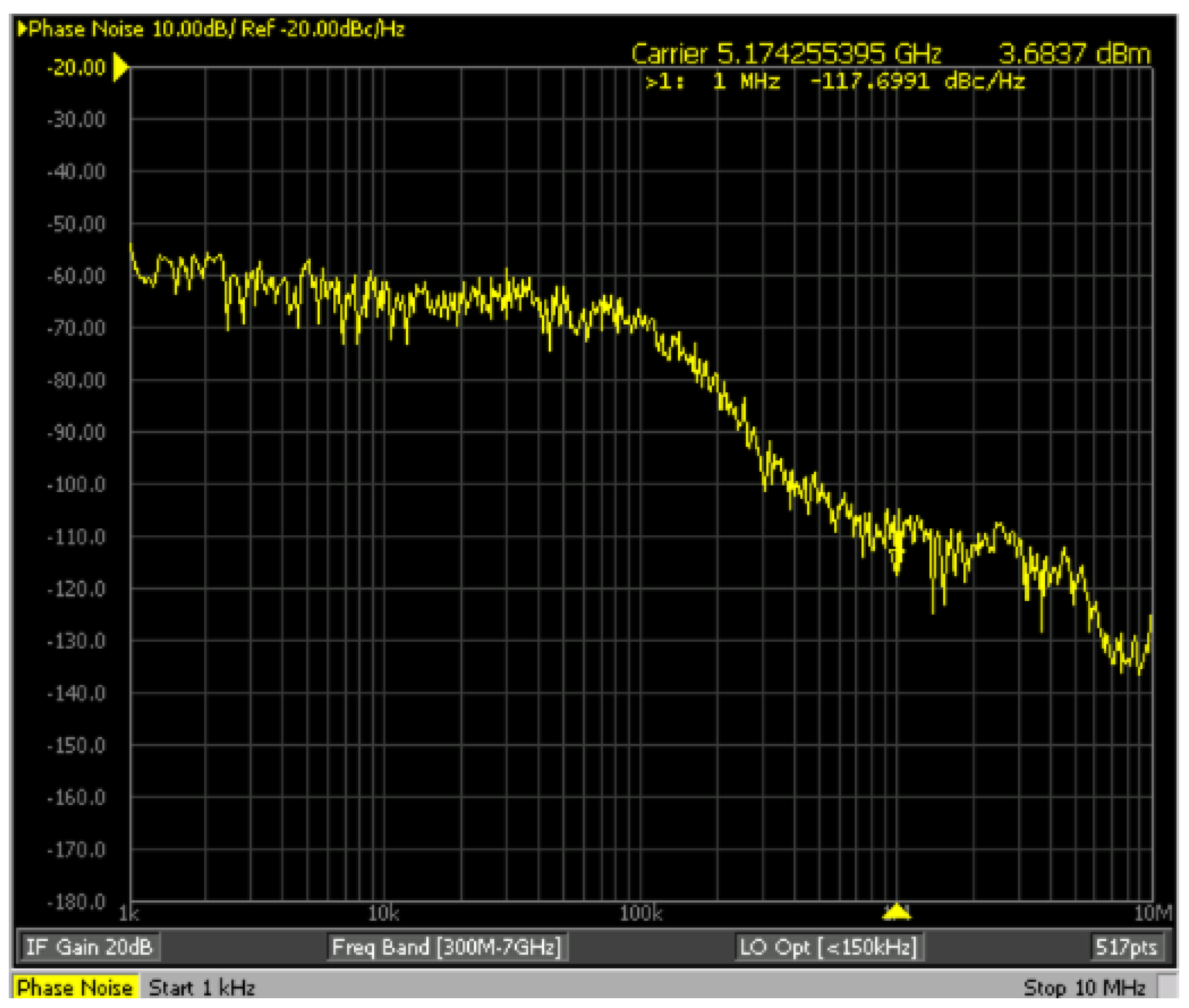
Figure 10.
Measured spectrum of the VCO at 5.065-GHz.
4. Conclusions
In this work, a low-power, wide-tuning-range voltage-controlled oscillator (VCO) for C-band applications has been proposed and successfully implemented using the TSMC 0.18 μm 1P6M CMOS process. The design incorporates several techniques such as body-biasing and an optimized varactor structure to enhance tuning range and reduce power consumption, while maintaining low phase noise. The measured phase noise at a 1 MHz offset is as low as −117.6 dBc/Hz, and the achieved figure-of-merit (FOM) is −188.6 dBc/Hz. The VCO achieves a tuning range of 1124 MHz with a core power consumption of only 3.4 mW. These results demonstrate the proposed VCO’s suitability for modern low-power communication systems, particularly in compact and battery-constrained IoT and 5G applications.
Author Contributions
Conceptualization, J.-J.H.; Methodology, J.-J.H. and Y.-C.L; Software, Y.-C. L.; Formal analysis, Y.-C.L; Data curation, J.-J.H.; Writing – review & editing, J.-J.H.; Supervision, S.J.H.Y.
Funding
This research received no external funding.
Data Availability Statement
No new data were created or analyzed in this study. Data sharing is not applicable to this article.
Conflicts of Interest
The authors declare no conflicts of interest.
References
- Singh, S.; Arya, R.K.; Sahana, B.C. RF Circuits for 5G Applications: Designing with mmWave Circuitry, 1st ed.; Wiley-Scrivener: USA, 2023. [Google Scholar]
- Sobot, R. Wireless Communication Electronics: Introduction to RF Circuits and Design Technique, 2nd ed.; Springer: Switzerland, 2021. [Google Scholar]
- Free, C.E.; Aitchison, C.S. RF and Microwave Circuit Design: Theory and Applications, 1st ed.; Wiley: USA, 2021. [Google Scholar]
- De Cock, W.; Steyaert, M.A. CMOS 10GHz voltage controlled, LC-oscillator with integrated high-Q inductor. In Proceedings of the 27th European Solid-State Circuits Conference, Villach, Austria; 2001; pp. 498–501. [Google Scholar]
- Hung, C.M.; Shi, L.; Lagnado, I.; O, K.K. A 25.9-GHz Voltage-controlled oscillator fabricated in a CMOS process. 2000 Symposium on VLSI Circuits. Digest of Technical Papers (Cat. No.00CH37103), Honolulu, HI, USA, 2000; pp. 100–101. [Google Scholar]
- Razavi, B. Design of Analog CMOS Integrated Circuits, 2nd ed.; McGraw-Hill Education: New York, USA, 2017. [Google Scholar]
- Lesson, D.B. A simple model of feedback oscillator noise spectrum. Proceedings of the IEEE, 1966, 54, 329–330. [Google Scholar] [CrossRef]
- Hajimiri, A.; Lee, T.H. A general theory of phase noise in electrical oscillators. IEEE J. Solid-State Circuits, 1998, 33, 179–194. [Google Scholar] [CrossRef]
- Hajimiri, A.; Lee T., H. Design Issuse in CMOS Differential LC Oscillators. IEEE J. Solid-State Circuits 1999, 34, 717–724. [Google Scholar] [CrossRef]
- Hajimiri, A.; Lee, T.H. Oscillator Phase Noise: A Tutorial. IEEE J. Solid-State Circuits 2000, 35, 326–335. [Google Scholar]
- Jerng, A. .; Sodini, C.G. The impact of device type and sizing on phase noise mechanisms. IEEE J. Solid-State Circuits, 2005, 40, 360–369. [Google Scholar] [CrossRef]
- Perraud, L.; Bonnot, L.; Sornin, N.; Pinatel, C. Fully Integrated 10 GHz CMOS VCO for Multi-Band WLAN Applications. Proceedings of 29th Eurpean Solid-State Circuits Conference (ESSCIRC), 2003; pp. 353–356. [Google Scholar]
- Ham, D.; Hajimiri, A. Concepts and methods in optimization of integrated LC VCOS. IEEE J. Solid-State Circuits, 2001, 36, 896–909. [Google Scholar] [CrossRef]
- Liu, J.; Liao, H.; Huang, R. A 5-GHz low-phase noise CMOS VCO with swing boosting technique. Microwave and Optical Technology Letter, 2009, 51, 2061–2064. [Google Scholar] [CrossRef]
- Moon, Y.J.; Roh, Y.-S.; Jeong, C.-Y.; Yoo, C. A 4.39-5.26 GHz LC-Tank CMOS voltage controlled oscillator with small VCO-gain variation. IEEE Microw. Wirel. Compon. Lett., 2009, 19, 524–526. [Google Scholar] [CrossRef]
- Lo, Y.-C.; Silva-Martinez, J. A 5-GHz CMOS LC quadrature VCO with dynamic current-clipping coupling to improve phase noise and phase accuracy. IEEE Trans. Microw. Theory Tech., 2013, 61, 2632–2640. [Google Scholar] [CrossRef]
Figure 2.
Simulated impedance and quality factor versus frequency characteristics in the LC tank.
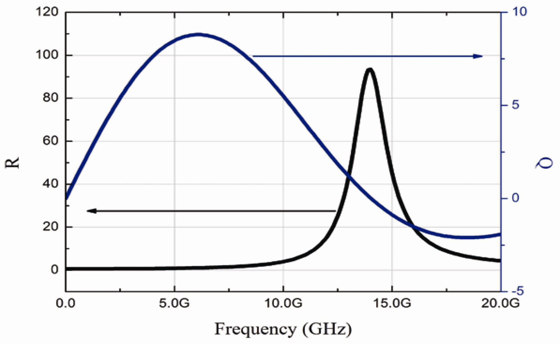
Figure 3.
Simulation C-V curve of the PMOS varactor.
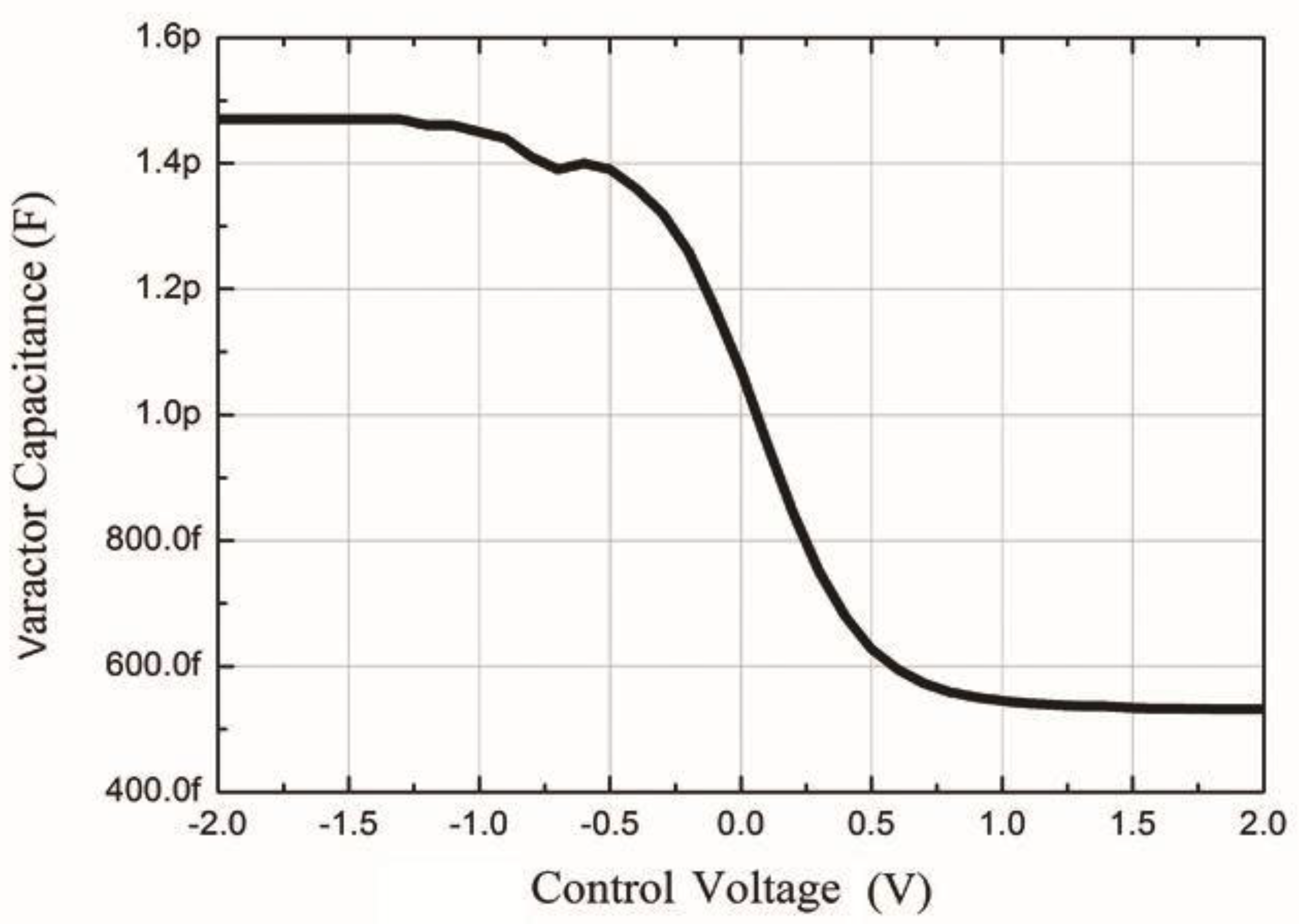
Figure 4.
Circuit schematic of the VCO.
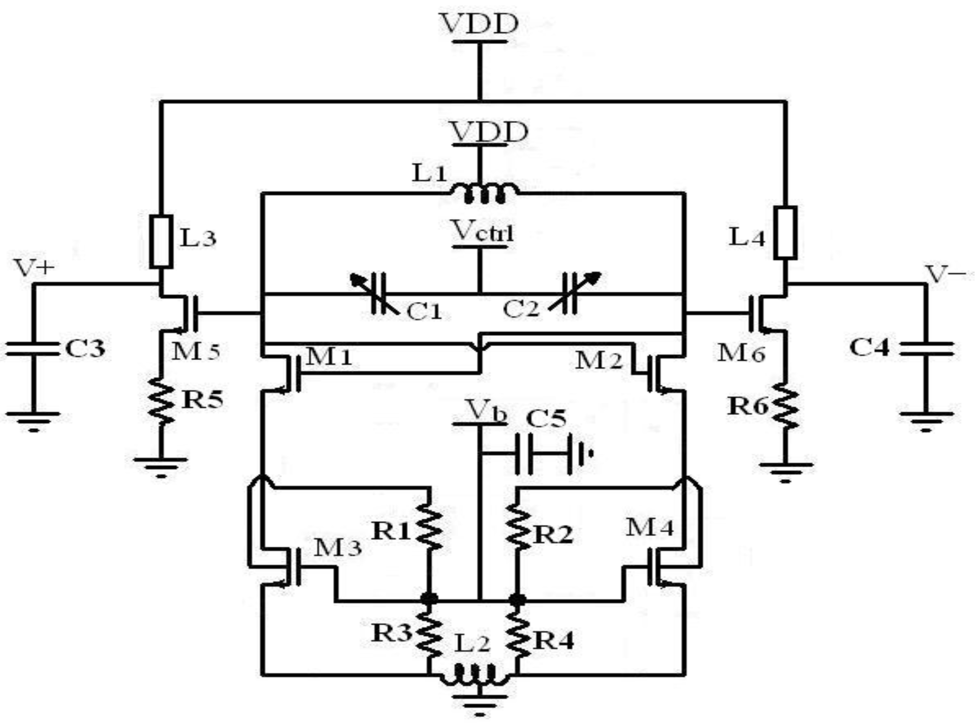
Figure 5.
Simulation result of the phase noise.
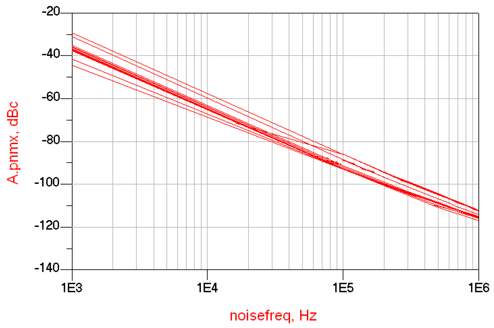
Figure 6.
Simulated tuning range of the VCO.
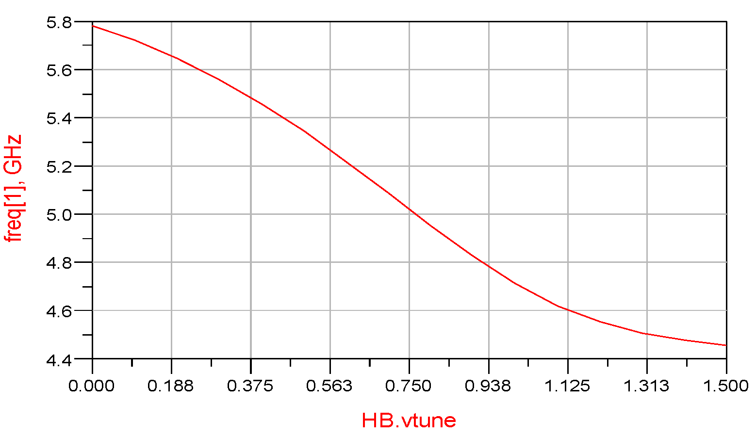

Table 1.
Comparison between post-simulation and measured results of the proposed VCO.
| Post-simulation | Measurement | |
|---|---|---|
| Frequency (GHz) | 5 | 5.06 |
| Tuning range (MHz) | 1324 | 1124 |
| Phase Noise (dBc/Hz) | -116.5 | -117.69 |
| FOM (dBc/Hz @MHz) | -181.4 | -196.6 |
| Output Power (dBm) | -4.6 | -22.44 |
| Power Consumption (mW) | 8.1 | 3.4 |
| Chip size (mm2) | 0.499 | |
Table 2.
Performance comparison with other reported VCOs.
| Ref. | CMOS Tech. (μm) |
Frequency (GHz) |
Phase Noise, dBc/Hz @1MHz | Tuning Range (%) | FOM (dBc/Hz) | PDC (mW) |
PFTN (dB) |
|---|---|---|---|---|---|---|---|
| [11] | 0.18 | 5.3 | -124 | 8 | -190 | 13.5 | -9.09 |
| [14] | 0.18 | 5 | -122.7 | 6.4 | -189.3 | 5.28 | -8.25 |
| [15] | 0.18 | 5.2 | -113.7 | 9.56 | -180 | 9.7 | N/A |
| [16] | 0.13 | 5 | -121 | 20 | -189 | 4.2 | N/A |
| This work | 0.18 | 5.06 | -117.7 | 22.2 | -188.6 | 3.4 | -4.3 |
Disclaimer/Publisher’s Note: The statements, opinions and data contained in all publications are solely those of the individual author(s) and contributor(s) and not of MDPI and/or the editor(s). MDPI and/or the editor(s) disclaim responsibility for any injury to people or property resulting from any ideas, methods, instructions or products referred to in the content. |
© 2025 by the authors. Licensee MDPI, Basel, Switzerland. This article is an open access article distributed under the terms and conditions of the Creative Commons Attribution (CC BY) license (http://creativecommons.org/licenses/by/4.0/).
Copyright: This open access article is published under a Creative Commons CC BY 4.0 license, which permit the free download, distribution, and reuse, provided that the author and preprint are cited in any reuse.


