
Submitted:
31 March 2025
Posted:
31 March 2025
You are already at the latest version
Abstract
We designed lens systems for SPOCNN using optical software to analyze image spread and estimate alignment tolerance for various kernel sizes. The design, based on a three-element lens, was reoptimized to minimize spot size while meeting system constraints. Simulations included root mean square spot and encircled energy diagrams, showing that geometric aberration increases with the scale factor, while diffraction effect remains constant. Alignment tolerance was determined by combining geometric image size with image spread analysis. While the preliminary scaling analysis predicted a limit at a kernel array size of 66 × 66, simulations showed that a size of 61 × 61 maintains sufficient alignment tolerance, well above the critical threshold. The discrepancy is likely due to lower angular aberration in the simulated optical design. This study confirms that an array size of 61 × 61 is feasible for SPOCNN, validating the scaling analysis for predicting image spread trends caused by aberration and diffraction.
Keywords:
optical neural network
; convolution
; smart pixel
1. Introduction
Deep learning has revolutionized various fields, including computer vision, speech recognition, and natural language processing, by leveraging artificial neural networks (ANNs) with deep architectures [1,2]. Among these, convolutional neural networks (CNNs) have become a fundamental tool for image and video analysis due to their ability to automatically extract hierarchical features such as edges, textures, and patterns [3]. CNNs achieve this by applying convolutional operations using kernels of different sizes, followed by pooling, nonlinear activation functions, and successive convolutional layers. These operations enable CNNs to recognize complex patterns in large datasets, making them highly effective for classification and object detection tasks. However, despite their superior performance, CNNs demand extensive computational resources, especially as the depth of the network and the size of the input images increase.
The computational complexity of CNNs is largely attributed to convolution operations, which scale with both image resolution and kernel size. For an image with n × n pixels convolved with a k × k kernel, the number of computations is proportional to n² × k², leading to substantial processing requirements. This challenge becomes more pronounced when dealing with real-time applications, where high latency and power consumption pose significant limitations. Although graphics processing units (GPUs) have been widely used to accelerate CNN inference through parallel processing, they suffer from inefficiencies such as high energy consumption and memory bandwidth constraints [4,5,6]. Furthermore, deploying CNNs on large-scale systems often requires multiple GPUs, which introduces additional communication overhead and synchronization delays [7,8]. These limitations highlight the necessity for alternative hardware architectures that can offer improved computational efficiency, reduced power consumption, and real-time processing capabilities, paving the way for innovations in specialized AI hardware and optical computing solutions.
To address the challenges of CNNs, researchers are increasingly exploring the feasibility of optical convolutional neural networks (OCNNs). Traditionally, OCNNs have been implemented using the 4f correlator system [9,10,11,12], which leverages Fourier optics for convolution operations [13]. While this approach offers certain advantages, it also has inherent limitations that hinder its practicality in optical neural networks. One major drawback is the limited scalability of input images due to the finite space-bandwidth product (SBP) of the lens used for Fourier transformation [9]. This issue is further exacerbated by geometric aberrations, which degrade the optical system’s resolution as image size increases.
Another significant limitation is the latency introduced by spatial light modulators (SLMs), which are essential for generating coherent optical inputs. Most SLMs operate at relatively low speeds, typically in the kilohertz range [14,15], significantly reducing the potential parallelism of optical computing. This becomes particularly problematic in multilayer optical neural networks, where the output of one layer serves as the input for the next. The need to update SLM pixels at each layer transition introduces additional delays, ultimately reducing throughput. Furthermore, reconfiguring convolution kernels in a 4f system is computationally intensive, as the kernel representation is based on its Fourier transform. This additional computational requirement further slows real-time processing, making the 4f correlator system less suitable for scalable and efficient optical deep learning applications.
To solve these problems, we first proposed a scalable optical convolutional neural network (SOCNN) [16] based on free-space optics utilizing a lens array and an SLM. Later, we improved the original design by replacing the SLM with a smart-pixel light modulator (SPLM) [17,18,19,20]. This improved architecture is referred to as the smart-pixel-based optical convolutional neural network (SPOCNN) [19]. The introduction of the SPLM resolves several issues related to the slow switching speed and limited cascading capability of the SLM. Additionally, the fast refresh rate and memory capabilities of the SPLM enable the development of other architectures, such as the smart-pixel-based bidirectional optical convolutional neural network (SPBOCNN) and the two-mirror-like SPBOCNN (TML-SPBOCNN) [19]. These two derived architectures are highly effective in making the SPOCNN scalable in both transverse and longitudinal directions across layers. The enhanced scalability makes the SPOCNN more adaptable, allowing it to handle large input array sizes and an arbitrary number of convolution layers based on software, without the need for expanded hardware resources.
In the previous study [19], the SPOCNN architecture was proposed only conceptually, with its performance analyzed through rough estimations. Consequently, many researchers may have questioned the feasibility of the SPOCNN design. Additionally, scaling analysis indicated that the kernel size was primarily limited by geometric aberrations. While this limitation can theoretically be overcome by implementing clustering methods [21] or software-based scaling with smart pixel memory [19,20], these approaches introduce additional hardware requirements or processing delays. Therefore, it is crucial to evaluate the performance and scaling limits of concrete SPOCNN designs before implementing specialized scaling techniques.
In this study, we verify the optical design of the SPOCNN using optical design software. We present design examples with various kernel sizes, utilizing three-element lenses optimized through optical design software. Performance is evaluated by analyzing spot size and encircled energy diagrams to estimate alignment tolerance, minimize crosstalk between channels, and examine the overall scalability of the SPOCNN.
2. Materials and Methods
Before presenting the optical designs of SPOCNNs, it is useful to first explain the fundamental concepts of the architecture. This allows for a more effective comparison between the performance estimations from previous studies and those obtained through simulations using concrete optical designs. The schematic in Figure 1a illustrates an SPOCNN comprising SPLMs, lenses, and photodetectors (PDs), along with mathematical formulas representing convolution.
The input signal originates from PD(0) in the zeroth layer and is sent to the electronic processor (EP) in the same layer, which is connected to SPLM(0) on the substrate. The internal structure of the SPLM is depicted in Figure 1b, where the electrical fan-out distributes the input signal across multiple pixels. Within the SPLM, EPs amplify the input signal according to the weight values stored in memory and then transmit the processed signal to the light-emitting diode (LED) within the same pixel. Each set of weight values controlled by an SPLM subarray corresponds to a kernel or filter in the SPOCNN.
The LED in the SPLM emits light, which then passes through a lens that refracts the beams based on their relative positions to the optical axis. The varying ray angles allow the transmission of signals from a single input node to multiple PDs in the first layer. PD(1) collects the light from multiple SPLMs, performing convolution calculations. The computed results are then sent to the EP connected to the PD, where additional operations such as bias addition and activation functions (e.g., sigmoid function) are applied. The final output is then forwarded to SPLM(1) in the first layer.
Because the pixels in SPLM(0) are optically conjugate to PD(1) via the lens, the image of an SPLM pixel is sharply projected onto the PD(1) plane. The magenta dotted line in Figure 1a represents the marginal ray of the projection lens, demonstrating this conjugation relationship, while the other rays, known as chief rays, indicate the positions of pixel images relative to one another.
Although Figure 1a illustrates a one-dimensional array of SPLMs, lenses, and PDs, this structure can be readily extended to a two-dimensional array, as shown in Figure 1c. The example in Figure 1c depicts a 3 × 3 kernel array. The lens magnification is determined by the kernel array size [16,19]. Suppose the pixel size and pitch are denoted by ε and d, respectively, as shown in Figure 1c. The pitch of the kernel subarray, represented as b, is equal to both the pitch of the detectors in the first layer and the lens diameter. For an M × M kernel array, the kernel subarray size is given by Md, satisfying b = Md. Since the detector pitch corresponds to the magnified image of the pixel pitch, the relationship b = M'd holds, where M' is the lens magnification which is . Therefore, the lens magnification M' is equivalent to the kernel size M.
As mentioned in the introduction, SPOCNN does not have a limitation on input array size, unlike the 4f correlator system. However, it does have a scaling limit for the kernel array size, primarily due to the geometric aberration of the lens [16,19]. Consequently, the scaling limit of the kernel array depends on the lens design and its imaging performance. The previous scaling analysis was based on the assumption that the lens has an f/# of 2 and an angular aberration of approximately 3 mrad.
Before discussing the scaling properties of SPOCNN, it is useful to review how the scaling analysis was conducted in previous research [16,19]. The analysis began with a 5 × 5 kernel array, examining the lens’s spot size under specific constraints as the kernel size increased. If the image size of a pixel exceeded the detector pitch or the remaining alignment tolerance became too small for practical implementation, it was considered the limiting factor for the kernel array size.
A similar approach can be applied to analyzing the scaling limit of the SPOCNN kernel, despite the differences in optical setups between SPOCNN and SOCNN. SPOCNN utilizes a single projection lens, whereas SOCNN consists of both a condenser lens and a projection lens, comprising a three-lens system. However, the scaling limits are assumed to be similar, as the projection lens primarily determines the scaling characteristics. The only distinction is that the projection lens in SPOCNN consists of a single lens group, whereas in SOCNN, it comprises two lens groups forming a relay lens system.
Suppose SPOCNN has a 5 × 5 kernel array with a square pixel of 10 μm and a period of 40 μm. The side length of the square kernel subarray is 200 μm, which corresponds to the lens diameter and the detector pitch in the first substrate. According to the notations in Figure 1c, ε, d, and b are 10, 40, and 200 μm, respectively. As mentioned earlier, the lens magnification M is equal to the row size of the kernel array, which is 5. Consequently, the geometric image size of a pixel is 50 μm, corresponding to a 25% duty cycle of the detector pitch, as it accounts for 25% of the pixel pitch in the SPLM plane.
To estimate the geometric aberration spread, we must determine the distance l2 between the lens and the detector plane. Given that the lens has an f/# of 2, the focal length is 0.4 mm, as dictated by the given diameter b. Using the lens formula and magnification, l2 is calculated to be 2.4 mm. Assuming the lens has an angular aberration of 3 mrad, the image spread due to geometric aberration is 7.2 μm, which accounts for 3.6% of the detector pitch.
Regarding diffraction spread, the diameter of the Airy disc is given by . For a wavelength of 850 nm, this results in 20.4 μm, accounting for 10.2% of the detector pitch. Therefore, the total image spread sums up to 39% of the detector pitch. The remaining duty cycle of the detector pitch can serve as an alignment tolerance in either the detector plane or the SPLM pixel plane. Since pixel plane alignment is more critical, it must be managed with greater precision. The alignment tolerance in the pixel plane is 61% of the pixel pitch, approximately 24 μm, which can be readily achieved using modern optomechanical techniques.
If the kernel array size is scaled up by a factor of α, it expands to a 5α × 5α array. With fixed values of ε and d, b increases by a factor of α. As the lens diameter increases by a scale factor, the focal length must also increase proportionally to maintain the same f/#. Since the subarray row size equals the magnification, the magnification also scales up by α times. The maximum image height increases by α2 times, as both the maximum object height and magnification increase by α times. Additionally, l1 and l2 grow by approximately α and α2 times, respectively.
To determine the critical factor in the scaling limitation, we analyze the effects of scaling on geometric image size, geometric aberration, and diffraction spread. When the kernel array is scaled up by a factor of α, the geometric image size of a pixel increases proportionally due to the increase in magnification. However, the duty cycle of the pixel image in the detector pitch remains constant since the detector pitch also scales by α. In terms of geometric aberration, the image spread due to aberration increases by α2 because l2 increases α2 times, while the angular aberration remains approximately constant. Consequently, the duty cycle of image spread due to aberration increases by α within the detector pitch, making geometric aberration a more significant factor as the kernel size scales up.
Similarly, diffraction spread also increases by α, following the relation , where λ is the wavelength. Since the lens aperture increases by α and l2 increases by α2, the duty cycle of diffraction spread in the detector pitch remains unchanged with scale-up. Thus, while diffraction effects remain constant, geometric aberration becomes the primary limiting factor in scaling. If the minimum alignment tolerance is set to a duty cycle of 13%, the remaining duty cycle available for geometric aberration is 48%. Given that the aberration of a 5 × 5 kernel array occupies 3.6% of the duty cycle, the maximum feasible scale-up factor is approximately 13.3, leading to a kernel array of about 66 × 66, as noted in previous studies [16,19]. The minimum alignment tolerance in the SPLM plane corresponds to approximately 5 μm, which can be achieved using modern optical packaging techniques.
This estimation of the scaling limit is based on approximations and several assumptions. Therefore, a more precise assessment would require simulations using optical design software applied to specific lens designs.
3. Results
A design example of SPOCNN is presented in Figure 2. The optical design was performed using CodeV (Ver. 2023.03). The initial design was based on US Patent 2,298,090, retrieved through the patent lens search feature in CodeV. This initial design consisted of a three-lens system with an infinite conjugate configuration. However, since SPOCNN operates as a finite conjugate system with a limited object distance, the lens arrangement was flipped and scaled to accommodate the maximum object height. The initial kernel array size was set to 61, as a larger array size closely approximates the infinite conjugate system of the original design. This similarity required fewer modifications during the optimization process when transitioning from an infinite to a finite conjugate system.
The maximum object height is determined by the kernel array size and pixel pitch. Given that the pixel size and pitch are set to 10 μm and 40 μm, respectively, the side length of the kernel array measures 2.44 mm, which also defines the maximum lens diameter. The object heights were set at 0.0 mm, 1.24 mm, and 1.86 mm. Notably, the third field value of 1.86 mm slightly exceeds 1.72 mm, which represents the distance from the center to the corner of the kernel subarray. The effective focal length and entrance pupil diameter were set to 6.2 mm and 2.48 mm, respectively, yielding an f/# of 2.5. The design utilizes a wavelength of 850 nm.
The lens parameters were further optimized to minimize spot size while meeting target specifications, such as effective focal length and magnification. The final optimized lens data is shown in Figure 2a, with the lens structure and its magnified view depicted in Figure 2b and Figure 2c, respectively. The corresponding spot diagram and encircled energy diagram are displayed in Figure 2d and Figure 2e. As seen in the second field of Figure 2d, the largest root-mean-square (RMS) spot diameter is 360 μm. Given that the distance from the last lens surface to the image plane is 365 mm, the resulting angular aberration is approximately 1 mrad. The encircled energy diameter, incorporating both geometric aberration and diffraction effects, is 647 μm, as shown in Figure 2e. Within this diameter, 80% of the total energy is contained.
In this design, the encircled energy diameter accounts for 26% of the detector pitch, which measures 2.48 mm. Considering that the geometric image of a pixel occupies 25% of the detector pitch, the remaining duty cycle is 49%, which can be utilized for alignment tolerance. This 49% duty cycle corresponds to 19.6 μm in the pixel plane, ensuring ease of alignment.
To demonstrate different kernel array sizes, we first scale down and then reoptimize the lens parameters with reduced magnification constraints. The tested array sizes, or magnifications, include 31, 21, 11, and 5. The simulation results are presented as lens views, spot diagrams, and encircled energy diagrams, as shown in Figures 3, 4, and 5, respectively. As the magnification decreases, the image distance decreases proportionally to the square of the scale-down factor, as illustrated in Figure 3.
As shown in Figure 4, the maximum RMS spot sizes occur in the second field rather than at the third field point. The resulting spot sizes are 94 μm, 45 μm, 16 μm, and 4 μm for magnifications (M) of 31, 21, 11, and 5, respectively. The spot size decreases approximately in proportion to the square of the scale-down factor, as predicted by the scaling analysis in the previous section. This result indicates that the angular aberration remains around 1 mrad, even after the reoptimization of the lens parameters.
As shown in Figure 5, the encircled energy fractions are plotted as a function of diameter for various kernel sizes. As the kernel size decreases, the encircled energy diameter also decreases. Since the encircled energy diameter is determined by both aberration and diffraction, the final image size is the sum of this encircled energy diameter and the geometric image size. Therefore, this diameter can be used to assess the alignment tolerance for different kernel sizes.
4. Discussion
The simulation results for various kernel sizes are summarized in Table 1. The encircled energy diameters were obtained from the software's text output and can be converted into the duty cycle within the detector pitch using the detector pitch value. This duty cycle, along with the duty cycle of the geometric image size (25%), can be used to determine the remaining duty cycle available for alignment tolerance. Since the duty cycle within the detector pitch is equivalent to that within the pixel pitch, it can be converted into the alignment tolerance in the pixel plane, measured in micrometers, as shown in Table 1.
For a kernel size of 31, the RMS spot diameter is 94 μm, accounting for 7.6% of the detector pitch. If the contribution of the RMS spot size is subtracted from the duty cycle of the encircled energy diameter (22%), the remaining duty cycle of 14% can be attributed to diffraction effects. The portion of aberration decreases approximately in proportion to the square of the scale-down factor. For a kernel size of 5, the RMS spot diameter is 4 μm, accounting for 2% of the detector pitch. Thus, the duty cycle attributed to diffraction remains approximately 14%, the same as that for a kernel size of 31. Although the diffraction duty cycle obtained from the simulation differs slightly from the 10% expected from the scaling analysis in the previous section, it remains consistent as the kernel size decreases.
The last column of the Table 1 shows the alignment tolerance in the pixel plane. Although it decreases as the kernel size increases, it does not reach the critical level of difficulty for the array size of 61 × 61. In the scaling analysis of the previous section, a kernel size of 66 has an alignment tolerance of only 5 μm, which is considered the limit of practical alignment. It may be ascribed to the different assumption on the angular aberration of the three-element lens. The angular aberrations of the designs in the simulation are usually about 1 mrad which is 3 times smaller than that assumed in the preliminary scaling analysis.
Therefore, the actual optical designs confirm that an array size of 61× 61 is feasible for the SPOCNN architecture with a reasonable alignment tolerance. They also validate that the previous scaling analysis is generally accurate in predicting the trends of image spread caused by geometric aberration and diffraction as the kernel array size increases.
5. Conclusions
We designed the lens system for SPOCNN using optical software for various kernel sizes and calculated the image spread to estimate the alignment tolerance. The design, based on a three-element lens, was flipped and scaled up to accommodate the characteristics of SPOCNN. Additionally, the designs were reoptimized to minimize spot size while meeting the constraints required for SPOCNN.
The simulation results include the RMS spot diagram and the encircled energy diagram. The RMS spot diameter demonstrates that geometric aberration increases proportionally to the square of the scale factor, as predicted by the preliminary scaling analysis. In terms of the duty cycle within the detector pitch, the duty cycle of the RMS spot size increases in proportion to the scale factor, while the duty cycle attributed to diffraction remains constant. By combining this with the geometric image size, we calculated the available duty cycle for alignment tolerance, ultimately determining the alignment tolerance in the pixel plane for various kernel sizes. Although the preliminary scaling analysis predicted a limit at a kernel size of approximately 66, the simulations indicate that a size of 61 still maintains sufficient alignment tolerance, well above the critical threshold. This discrepancy may be due to the angular aberration in the optical designs from the simulations being much smaller than the assumption made in the preliminary analysis.
This study confirms that a kernel array size of 61 × 61 is viable for the SPOCNN architecture, providing sufficient alignment tolerance. It also validates that the previous scaling analysis generally predicts trends in image spread caused by geometric aberration and diffraction as the kernel array size increases.
Funding
This research received no external funding.
Data Availability Statement
The datasets generated during and/or analyzed during the current study are available from the corresponding author on reasonable request.
Conflicts of Interest
The authors declare no conflicts of interest.
References
- Hinton, G.; Deng, L.; Yu, D.; Dahl, G.E.; Mohamed, A.R.; Jaitly, N.; Senior, A.; Vanhoucke, V.; Nguyen, P.; Sainath, T.N.; et al. Deep neural networks for acoustic modeling in speech recognition: The shared views of four research groups. IEEE Signal Process. Mag. 2012, 29, 82–97. [Google Scholar] [CrossRef]
- LeCun, Y.; Bengio, Y.; Hinton, G. Deep learning. Nature 2015, 521, 436–444. [Google Scholar] [CrossRef] [PubMed]
- Lecun, L.; Bottou, L.; Bengio, Y.; Haffner, P. Gradient-based learning applied to document recognition. Proc. IEEE 1998, 86, 2278–2324. [Google Scholar] [CrossRef]
- Chetlur, S.; Woolley, C.; Vandermersch, P.; Cohen, J.; Tran, J.; Catanzaro, B.; Shelhamer, E. cuDNN: Efficient primitives for deep learning. arXiv 2014, arXiv:1410.0759v3. [Google Scholar]
- Han, S.; Pool, J.; Tran, J.; Dally, W. Learning both weights and connections for efficient neural network. Adv. Neural Inf. Process. Syst. 2015, 28, 1135–1143. [Google Scholar]
- Rhu, M.; Gimelshein, N.; Clemons, J.; Zulfiqar, A.; Keckler, S.W. vDNN: Virtualized deep neural networks for scalable, memory-efficient neural network design. In Proceedings of the 2016 49th Annual IEEE/ACM International Symposium on Microarchitecture (MICRO), Taipei, Taiwan, 15–19 October 2016; pp. 1–13. [Google Scholar]
- Chen, T.; Moreau, T.; Jiang, Z.; Zheng, L.; Yan, E.; Shen, H.; Cowan, M.; Wang, L.; Hu, Y.; Ceze, L.; et al. TVM: An automated end-to-end optimizing compiler for deep learning. In Proceedings of the 13th USENIX Symposium on Operating Systems Design and Implementation (OSDI 18), Carlsbad, CA, USA, 8–10 October 2018; pp. 578–594. [Google Scholar]
- Jouppi, N.P.; Young, C.; Patil, N.; Patterson, D.; Agrawal, G.; Bajwa, R.; Bates, S.; Bhatia, S.; Boden, N.; Borchers, A.; et al. In-datacenter performance analysis of a tensor processing unit. In Proceedings of the 44th Annual International Symposium on Computer Architecture, Toronto, ON, Canada, 24–28 June 2017; pp. 1–12. [Google Scholar]
- Colburn, S.; Chu, Y.; Shilzerman, E.; Majumdar, A. Optical frontend for a convolutional neural network. Appl. Opt. 2019, 58, 3179–3186. [Google Scholar] [CrossRef] [PubMed]
- Chang, J.; Sitzmann, V.; Dun, X.; Heidrich, W.; Wetzstein, G. Hybrid optical-electronic convolutional neural networks with optimized diffractive optics for image classification. Sci. Rep. 2018, 8, 12324. [Google Scholar] [CrossRef] [PubMed]
- Lin, X.; Rivenson, Y.; Yardimci, N.T.; Veli, M.; Luo, Y.; Jarrahi, M.; Ozcan, A. All-optical machine learning using diffractive deep neural networks. Science 2018, 361, 1004–1008. [Google Scholar] [CrossRef] [PubMed]
- Sui, X.; Wu, Q.; Liu, J.; Chen, Q.; Gu, G. A review of optical neural networks. IEEE Access 2020, 8, 70773–70783. [Google Scholar] [CrossRef]
- Goodman, J.W. Introduction to Fourier Optics; Roberts and Company Publishers: Greenwood Village, CO, USA, 2005. [Google Scholar]
- Cox, M.A.; Cheng, L.; Forbes, A. Digital micro-mirror devices for laser beam shaping. In Proceedings of the SPIE 11043, Fifth Conference on Sensors, MEMS, and Electro-Optic Systems, Skukuza, South Africa, 8–10 October 2018; Volume 110430Y. [Google Scholar]
- Mihara, K.; Hanatani, K.; Ishida, T.; Komaki, K.; Takayama, R. High Driving Frequency (>54 kHz) and Wide Scanning Angle (>100 Degrees) MEMS Mirror Applying Secondary Resonance For 2K Resolution AR/MR Glasses. In Proceedings of the 2022 IEEE 35th Inter-national Conference on Micro Electro Mechanical Systems Conference (MEMS), Tokyo, Japan, 9–13 January 2022; pp. 477–482. [Google Scholar]
- Ju, Y.G. Scalable Optical Convolutional Neural Networks Based on Free-Space Optics Using Lens Arrays and a Spatial Light Modulator. J. Imaging 2023, 9, 241. [Google Scholar] [CrossRef] [PubMed]
- Seitz, P. Smart Pixels. In Proceedings of the EDMO 2001/VIENNA, Vienna, Austria, 15–16 November 2001; pp. 229–234. [Google Scholar]
- Hinton, H.S. Progress in the smart pixel technologies. IEEE J. Sel. Top. Quantum Electron. 1996, 2, 14–23. [Google Scholar] [CrossRef]
- Ju, Y.-G. A Conceptual Study of Rapidly Reconfigurable and Scalable Optical Convolutional Neural Networks Based on Free-Space Optics Using a Smart Pixel Light Modulator. Computers 2025, 14, 111. [Google Scholar] [CrossRef]
- Ju, Y.-G. A Conceptual Study of Rapidly Reconfigurable and Scalable Bidirectional Optical Neural Networks Leveraging a Smart Pixel Light Modulator. Photonics 2025, 12, 132. [Google Scholar] [CrossRef]
- Ju, Y.G. A scalable optical computer based on free-space optics using lens arrays and a spatial light modulator. Opt. Quan-tum Electron. 2023, 55, 1–21. [Google Scholar] [CrossRef]
Figure 1.
Illustration of SPOCNN: (a) Diagram of SPOCNN with mathematical formulation. represents the i-th node in the l-th layer, while denotes the weight connecting the j-th input to the i-th output. The bias associated with the i-th node is given by . N defines the input array size, whereas Nm indicates either the kernel dimensions or the number of weights assigned to each node. The activation function σ corresponds to the sigmoid function; (b) Internal structure of the SPLM with electrical fan-out, as utilized in SPOCNN; (c) Three-dimensional representation of SPOCNN with a 3 × 3 input and 3 × 3 output. ε represents the size of the light source in the SPLM, while b and d indicate the spacing between detectors (or kernel subarrays) and smart pixels, respectively. L1 and l2 denote the distances from the lens to the SPLM and from the lens to the detector, respectively.
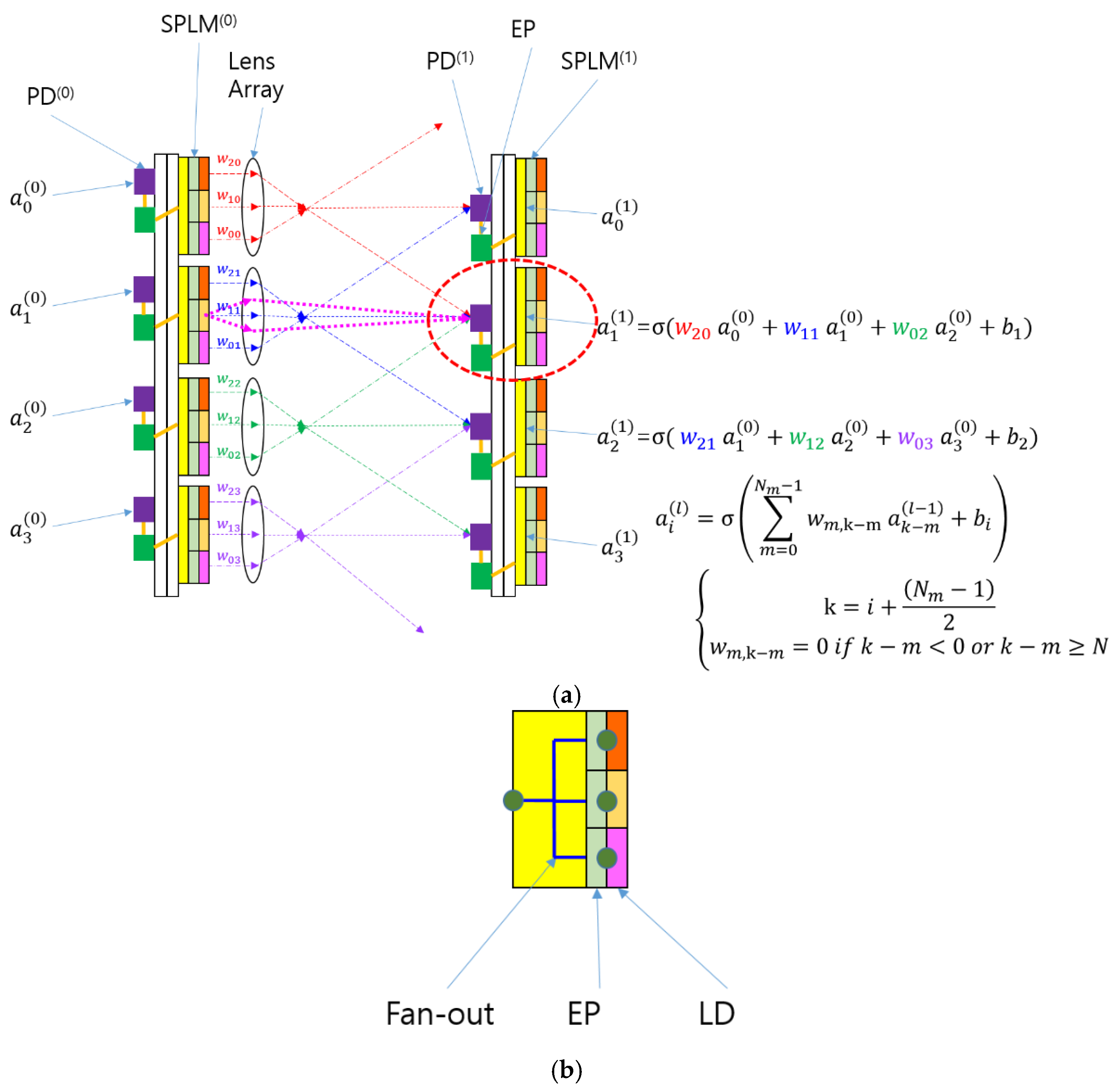
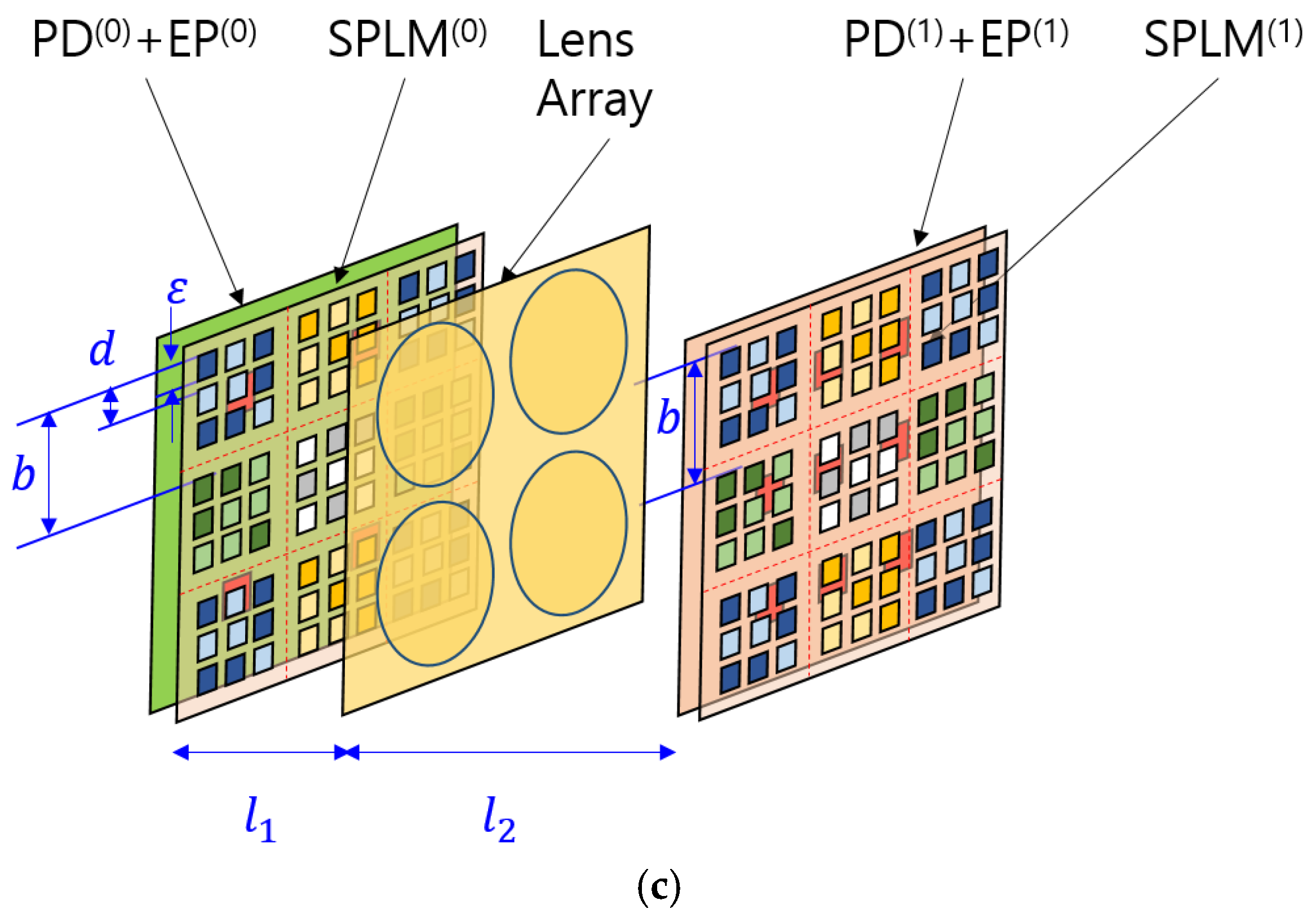
Figure 2.
An optical design example of SPOCNN with a magnification (M) of 61, corresponding to a 61 × 61 kernel array size. (a) Lens specifications; (b) Lens layout; (c) Magnified view of the lenses; (d) Spot diagram; (e) Diffraction encircled energy.
Figure 2.
An optical design example of SPOCNN with a magnification (M) of 61, corresponding to a 61 × 61 kernel array size. (a) Lens specifications; (b) Lens layout; (c) Magnified view of the lenses; (d) Spot diagram; (e) Diffraction encircled energy.
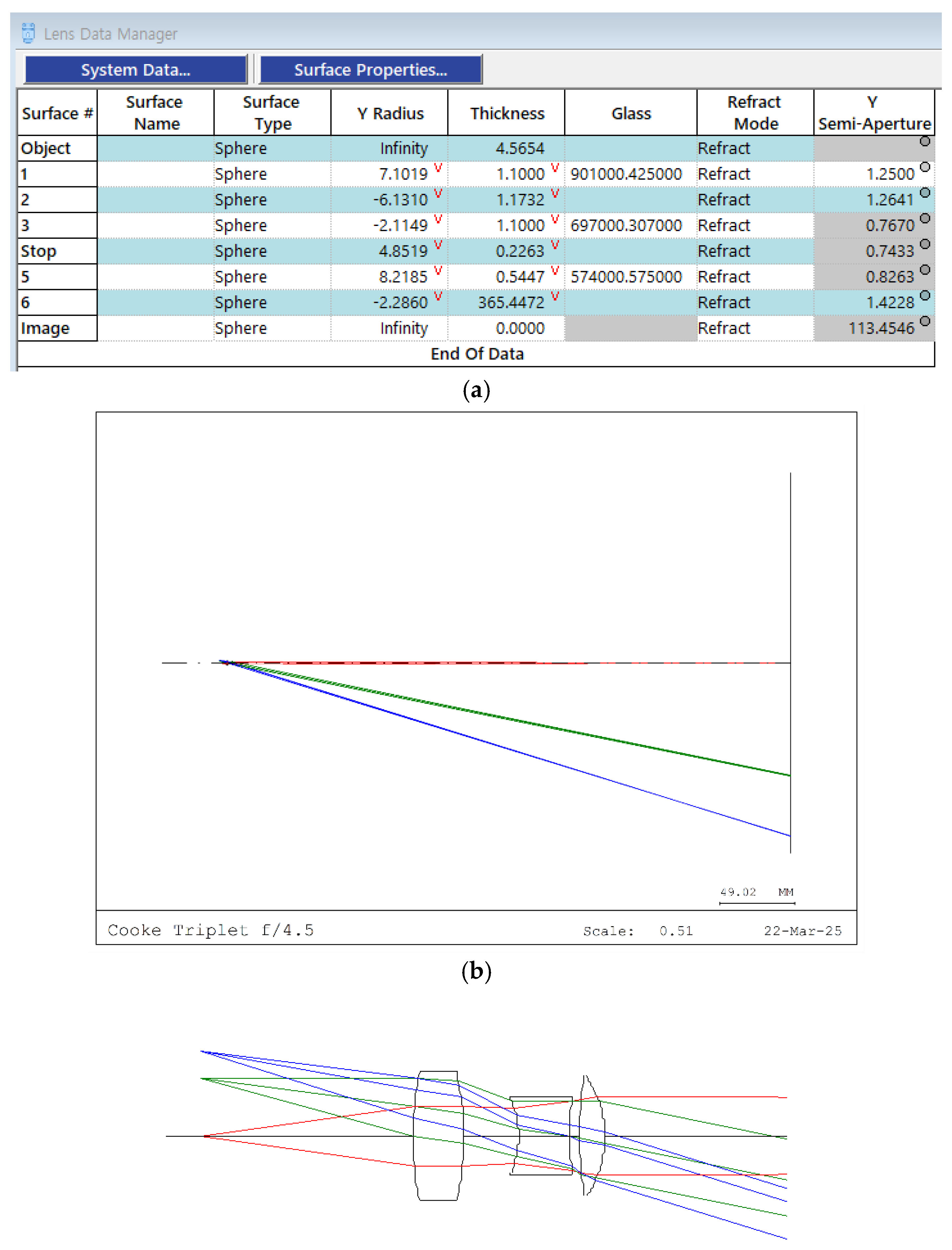
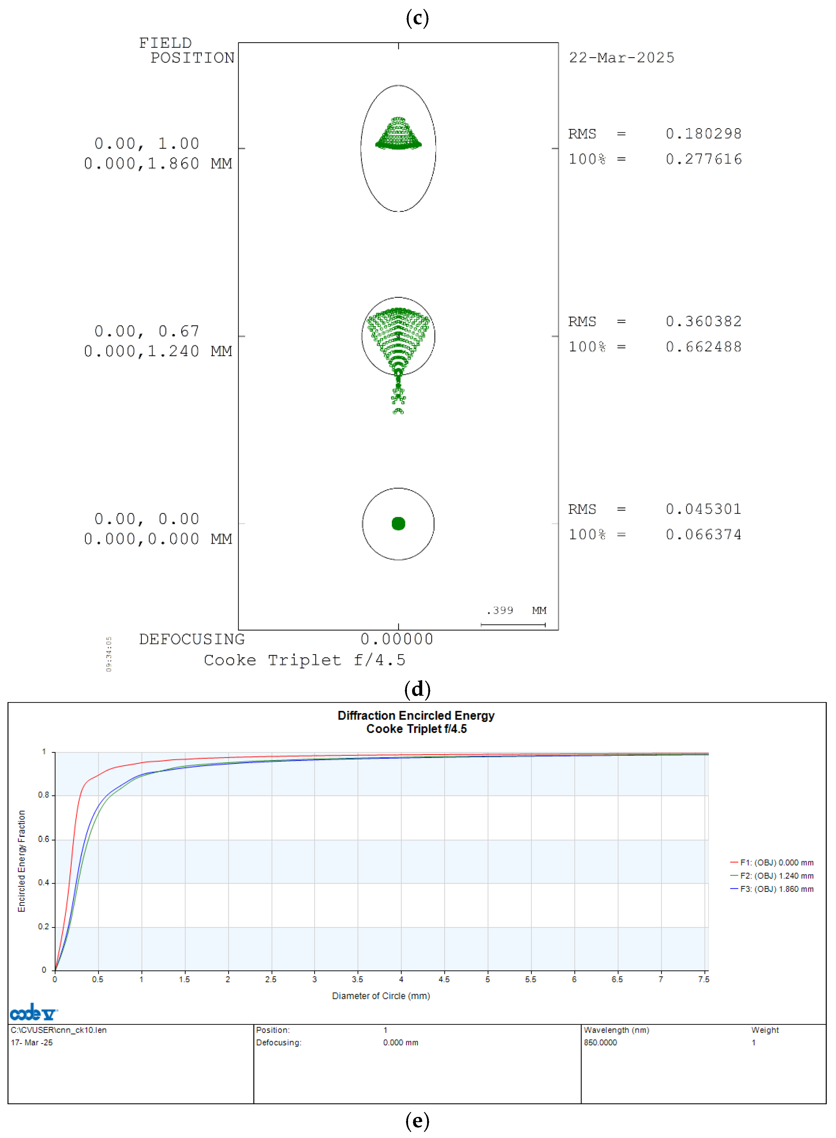
Figure 3.
Lens views at different magnifications: (a) M = 31; (b) M = 21; (c) M = 11; (d) M = 5.
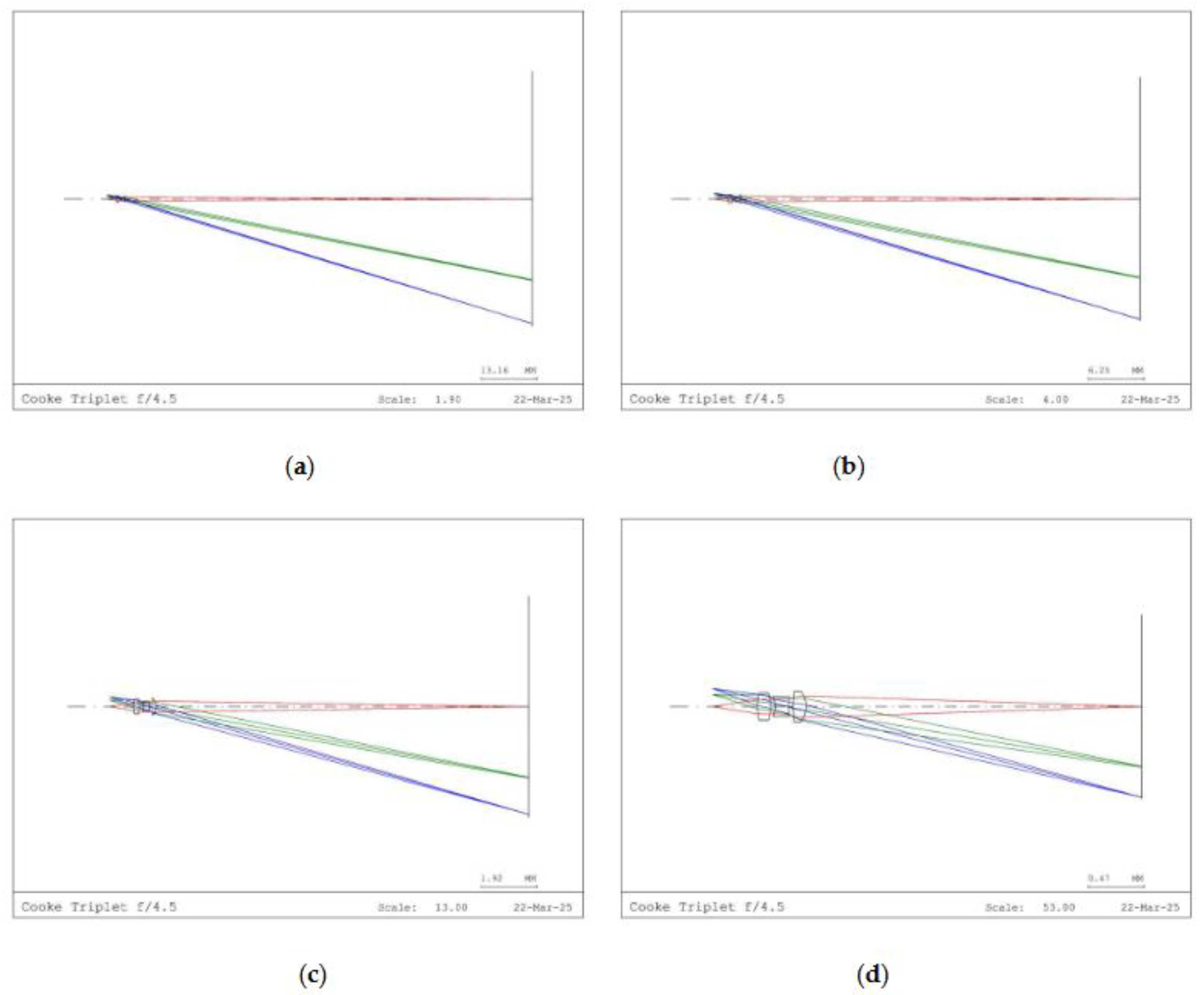
Figure 4.
Spot diagrams at different magnifications: (a) M = 31; (b) M = 21; (c) M = 11; (d) M = 5.
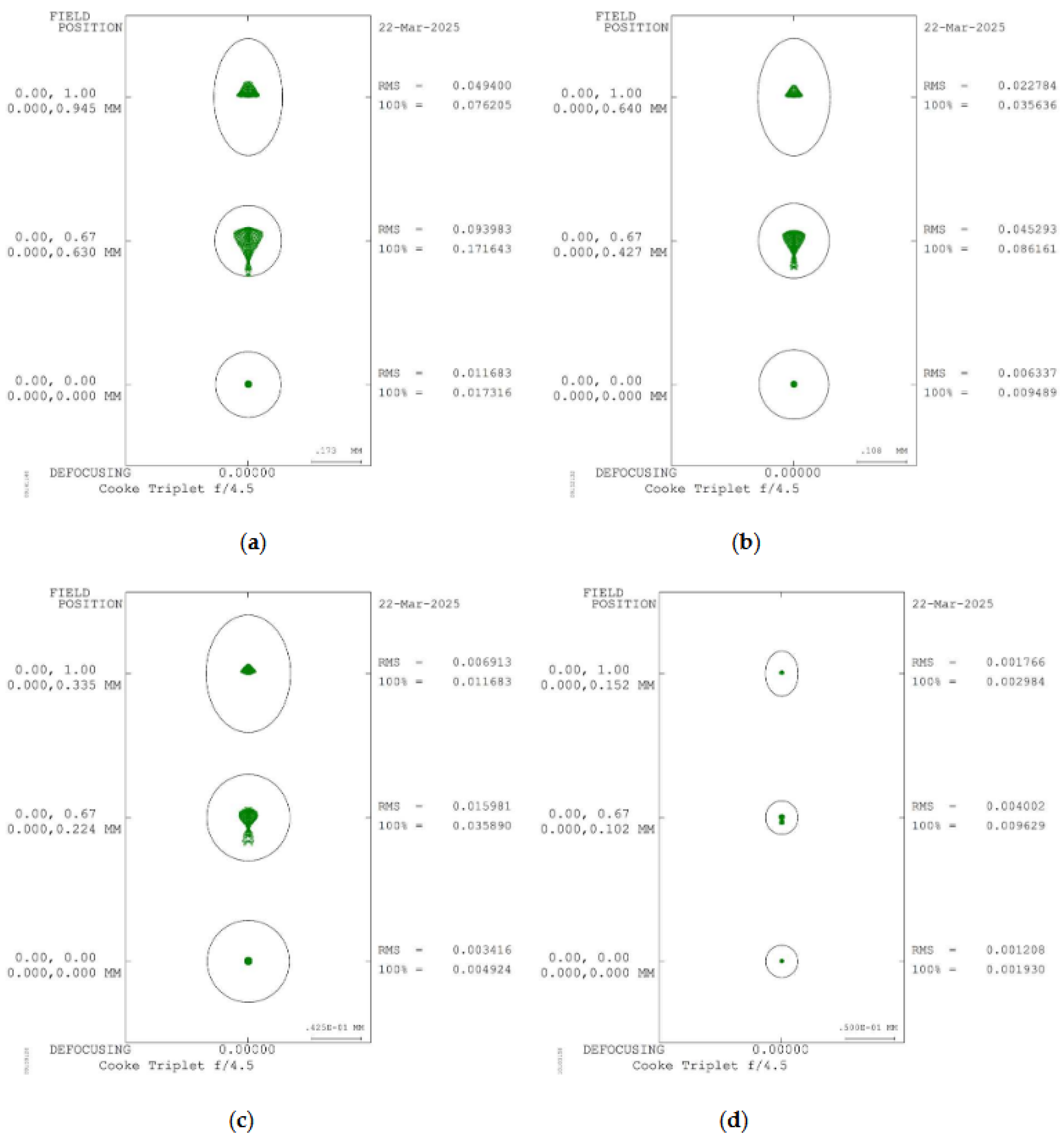
Figure 5.
Diffraction encircled energy diagrams at different magnifications: (a) M = 31; (b) M = 21; (c) M = 11; (d) M = 5.
Figure 5.
Diffraction encircled energy diagrams at different magnifications: (a) M = 31; (b) M = 21; (c) M = 11; (d) M = 5.
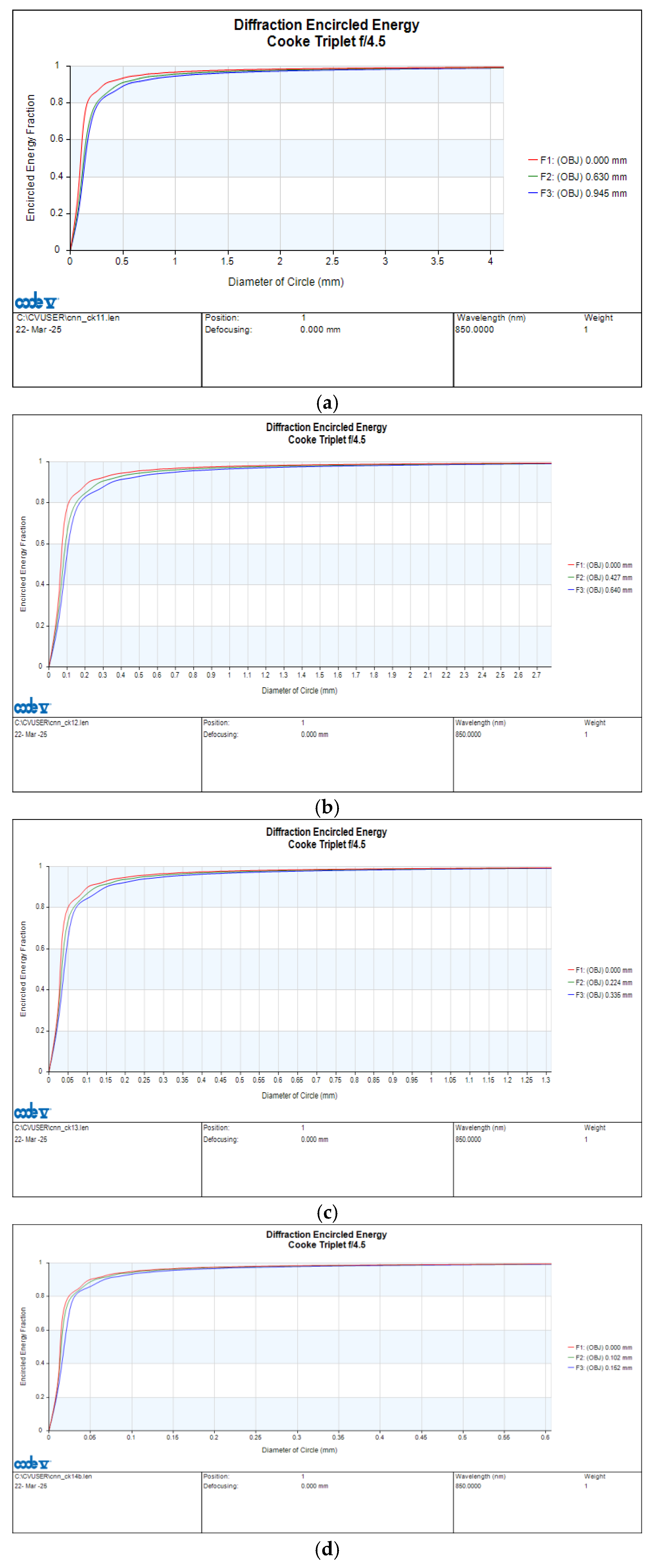

Table 1.
Image spread and alignment tolerance for various kernel array sizes.
| Kernel size (M) : M × M array |
RMS spot diameter (μm) |
Encircled energy diameter (μm) |
Detector pitch (μm) |
Duty cycle within detector pitch (%) |
Alignment tolerance in the pixel plane (μm) |
|---|---|---|---|---|---|
| 61 | 360 | 647 | 2480 | 26 | 19.6 |
| 31 | 94 | 274 | 1240 | 22 | 21.2 |
| 21 | 45 | 170 | 840 | 20 | 22.0 |
| 11 5 |
16 4 |
73 32 |
440 200 |
17 16 |
23.2 23.6 |
Disclaimer/Publisher’s Note: The statements, opinions and data contained in all publications are solely those of the individual author(s) and contributor(s) and not of MDPI and/or the editor(s). MDPI and/or the editor(s) disclaim responsibility for any injury to people or property resulting from any ideas, methods, instructions or products referred to in the content. |
© 2025 by the authors. Licensee MDPI, Basel, Switzerland. This article is an open access article distributed under the terms and conditions of the Creative Commons Attribution (CC BY) license (http://creativecommons.org/licenses/by/4.0/).
Copyright: This open access article is published under a Creative Commons CC BY 4.0 license, which permit the free download, distribution, and reuse, provided that the author and preprint are cited in any reuse.


