
Submitted:
26 March 2025
Posted:
27 March 2025
You are already at the latest version
Abstract
Colloidal quantum dots (QDs) and graphene hybrids have emerged as promising platforms for optoelectronic and biosensing applications due to their unique photophysical and electronic properties. This study investigates the fundamental mechanism underlying the photoluminescence (PL) quenching and recovery in graphene–QD hybrid systems using single-layer graphene field-effect transistors (SLG-FETs) and time-resolved photoluminescence (TRPL) spectroscopy. We demonstrate that PL quenching and its recovery are primarily driven by charge transfer, as evidenced by an unchanged fluorescence lifetime upon quenching. Density functional theory calculations reveal a significant charge redistribution at the graphene–QD interface, corroborating experimental observations. We also provide a simple analytical quantum mechanical model to differentiate charge transfer-induced PL quenching from resonance energy transfer. Furthermore, we leverage the charge transfer mechanism for ultrasensitive biosensing to detect biomarkers such as immunoglobulin G (IgG) at femtomolar concentrations. The sensor’s electrical response, characterized by systematic shifts in the Dirac point of SLG-FETs, confirms the role of analyte-induced charge modulation in PL recovery. Our findings provide a fundamental framework for designing next-generation graphene-based biosensors with exceptional sensitivity and specificity.
Keywords:
graphene
; quantum dots
; biosensing
; photoluminescence
; field-effect transistor
1. Introduction
Colloidal quantum dots (QDs) received significant attention in optoelectronic and sensing applications due to their high quantum yield, size-tunable band gap, narrow spectral emission, and robust photostability [1,2,3]. Their integration with two-dimensional (2D) materials, such as graphene, has opened new avenues for exploring light–matter interactions at the nanoscale [4,5]. Single-layer graphene (SLG) exhibits a linear energy dispersion at the K and K’ points in the Brillouin zone with the Fermi energy (EF) at the Dirac point [6,7]. The ability to tune EF in SLG with simple electrostatic gating or through SLG-QD hybrids paved the way for SLG-field effect transistors (SLG-FETs), which have been widely used as sensors [8,9,10,11,12]. Given the broad applicability of hybrid SLG-QD architectures for biomedical sensing to next-generation photovoltaics, understanding their interaction mechanisms is of particular interest.
Graphene is known to perturb the photoluminescence (PL) emission from a fluorophore or QDs in its close vicinity [13,14,15]. Kasry et al. showed that graphene is an efficient quencher of PL emission with quenching efficiency higher than gold [16]. Brus et al. reported a high quench factor of ∼ 25 for an CdSe/ZnS QDs on SLG surface [17]. Similarly, Federspiel et al. demonstrated that the quenching of CdSe QDs on MgO/graphene substrates shows d-4 distance dependence [13].
The recovery of PL emission from graphene-QD hybrids has been used widely in biosensors [18,19,20,21,22,23]. The first-ever application of quenching followed by Förster resonance energy transfer (FRET) at the QD-graphene oxide (GO) interface for biomolecular detection was proposed by Dong et al[24]. The sensing mechanism in such sensors relies on the disruption of quenching in the presence of the target analyte. In this methodology, it is proposed that when the analyte binds functionalized QDs immobilized on GO or SLG surface, the distance between the QDs and GO/SLG increases significantly hindering FRET. Consequently, PL emission from QDs is recovered [25,26,27,28,29]. However, this distance-dependent PL modulation has remained a subject of debate, particularly given the inconsistencies in the type of graphene used (e.g., SLG or few-layer graphene, exfoliated graphene, graphene oxide or GO, reduced graphene oxide or rGO etc). Alternative studies have proposed that PL quenching in graphene-QD systems may be attributed to mechanisms such as charge transfer rather than energy transfer[30,31,32,33].
In this study, we aim to clarify the underlying mechanism of PL quenching and recovery in graphene-QD hybrid sensors. Utilizing SLG-FET measurements and time-resolved photoluminescence (TRPL) spectroscopy, we show that quenching occurs through rapid charge transfer before optical excitation. Our findings indicate that the fluorescence lifetime remains unchanged upon quenching, supporting the charge transfer-induced static quenching mechanism. To further elucidate this mechanism, we present a heuristic quantum mechanical model demonstrating how analyte interactions with either QDs, SLG, or both can alter charge transfer characteristics, leading to PL recovery. This model offers a simple understanding of the PL modulation in graphene-QD hybrids, which is crucial for the rational design of advanced sensing platforms.
Building on the charge transfer quenching mechanism, we utilized two well-characterized biological interactions: biotin-streptavidin and immunoglobulin G (IgG)-anti-IgG antibody recognition to develop femtomolar biosensors with dual detection capability (optical and electrical). The biotin-streptavidin system is a model bioaffinity pair, widely used in biosensors due to its exceptionally strong binding affinity (dissociation constant Kd ≈ 10-15 M). We show that when biotin interacts with streptavidin-functionalized CdSe QDs, the resulting biomolecular interactions alter the charge transfer dynamics between the QD and graphene, disrupting the quenching effect and restoring QD fluorescence. We observed a linear PL recovery with increasing biotin concentration, with significant signal enhancement at femtomolar concentrations, highlighting the ultrasensitive nature of the detection mechanism. Similarly, we investigated the detection of IgG, a key biomarker in immune response and disease diagnostics. The interaction between IgG and its corresponding anti-antibody (anti-IgG) conjugated with CdSe QDs leads to charge redistribution at the graphene interface, modulating both optical and electrical properties. Notably, FET measurements revealed a systematic shift in the Dirac point voltage (VCNP) with increasing IgG concentration, confirming the doping effect of biomolecules on the graphene channel. The recovery of PL intensity was highly sensitive to IgG concentrations as low as 0.5 fM, underscoring the ability of our sensor to detect minute molecular changes. We found little to no change in the decay time of anti-IgG conjugated QD/SLG hybrids in the presence of different IgG concentrations further confirming the charge transfer mechanism.
2. Materials and Methods
2.1. Materials and Reagents
The SLG-FET sensor array (0.8 ), monolayer graphene on a 90 nm Si / SiO2 (10 mm2) and quartz substrate, all grown with chemical vapor deposition, were purchased from Graphenea Semiconductor SLU. The SLG-GFET array (model: mGFET-4D) comprises 28 graphene channels with Au metal pads passivated with 50 nm Al2O3 via atomic layer deposition. The non-encapsulated electrode at the center of the chip enables liquid gating. CdSe QDs (Invitrogen, Cat. # Q10123MP), anti-human IgG antibody (Ab) (Abcam, Cat.# ab109489), Biotin, bovine serum albumin (BSA), phosphate buffered saline (PBS), and Tween20 were purchased from Thermo Fisher Scientific. Sample preparation and CdSe QD- Antibody conjugation: A standard buffer was prepared by mixing 0.5% (v/v) of Tween-20 and 1% (w/v) of BSA in 0.01 M PBS. This standard buffer was used as a solvent for all further studies. A stock solution of conjugated CdSe QDs was prepared by mixing QDs with antihuman IgG antibody (Ab) to a final concentration of 100 nM for QDs and 200 g ml−1 for Ab on a continuous shaker for 30 mins.
2.2. Raman Spectroscopy and Fluorescence Measurements:
All Raman and fluorescence intensity measurements were performed at room temperature using Renishaw inVia micro spectrometer with 532 nm excitation laser at a laser power of 1 mW at the sample at 10x magnifications. All measurements were performed in triplicates and averaged to obtain the final spectrum.
2.3. Fluorescence Microscopy:
Fluorescence images at different stages of the experiment were captured using Zeiss Axio Imager A1 upright microscope equipped with a 120-watt metal halide lamp as a light source and Axiocam MRc 5 camera for live image recording. All imaging was carried out under Zeiss Filter set 20 (488020-0000) with excitation 546 nm and emission in the range of 575-640 nm with 20X/40X objectives.
2.4. Time-Resolved Fluorescence Measurements:
Fluorolog®-3 spectrometer with a NanoLED 375L pulsed laser source was used for all TRPL estudies. The detector monochromator was set at 655 nm with 15 nm bandpass for data acquisition. A custom 3D-printed sample holder was used to mount the sample substrate inside the instrument.
2.5. Electrical Measurements:
Following the desiccation of Streptavidin/ Ab conjugated QD on the graphene surface, the electrical measurements on the SLG-FET device were carried out using the portable printed circuit board (PCB) readout system. Two Keithley 2400 source/measure units (SMU) were used to measure the source-drain current Ids as a function of the gate voltage Vg. For the measurements, the source-drain voltage (Vds) was kept biased at 100 mV while the gate was swept in the -1.5-1.5 V window while measuring the Ids. A 500 ms delay was applied between the source and measurement to stabilize the applied gate voltage (step size- 1 mV). For all measurements, a dormancy period of 5 min. was maintained following the analyte drop cast.
2.6. Atomic Force Microscopy:
Surface morphology of SLG-FET device was analyzed using AFM workshop TT-2 with 50 x 50 x 17 m scanner and Budget sensor Tap190Al-G cantilevers of tip radius <10 nm and res= 190 kHz in vibrating mode. All scans were carried out in dry conditions and were analyzed via Gwyddion image analysis software.
2.7. Density Functional Theory (DFT):
An estimation of the charge transfer between graphene and CdSe QDs was performed using DFT-D2 approach. The calculations were performed using the Quantum ESPRESSO package with ultrasoft pseudopotentials for a plane wave basis set. The generalized gradient approximation (GGA) was applied with the Perdew-Burke-Ernzerhof (PBE) exchange-correlation functional, incorporating London dispersion interactions. Exact parameters, including cell dimensions, k-mesh, and energy cutoff for the plane wave basis, were obtained beforehand by optimizing each system individually. System staking was achieved by placing 4×4 supercell size (16 Cd and 16 Se atoms each) of CdSe system over 7×7 supercell size (98 carbon atoms) of graphene.
3. Results
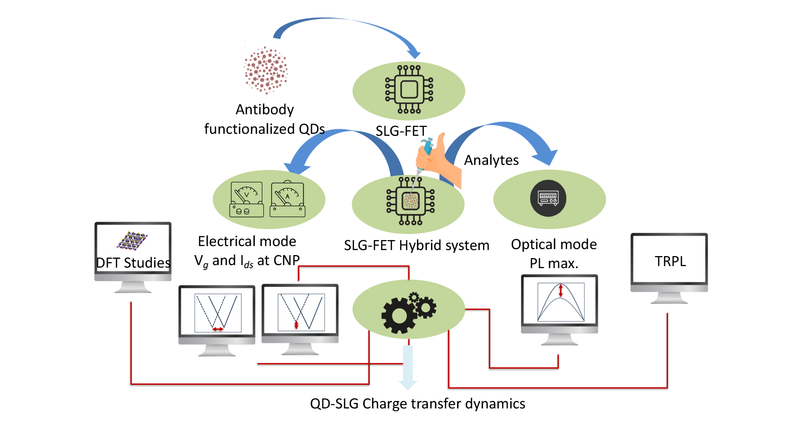
Our graphene-based sensing platform uses highly photoluminescent QDs pre-coated with detection antibodies that are deposited on the surface of SLG (Figure 1). Initially, PL emission from QDs is quenched by SLG. When the analyte binds the detection antibody, quenching is disrupted, and QD PL is restored, enabling analyte detection in a single step. We hypothesize that the quenching and restoration of QD PL is closely linked to the charge transfer (prior to optical excitation) between SLG and QDs. In order to simultaneously investigate both PL quenching and charge transfer, we adopted the experimental approach shown in Figure 1a by using SLG-FETs for both optical and electrical characterization.
The Raman spectra of single-layer graphene (SLG) on Si/SiO2 (Figure 1b) exhibited the characteristic sharp graphitic (G) and double-resonant harmonic of in-plane transverse optical phonon (2D) peaks. The ratio of integrated intensities of the 2D and G-band (I2D/IG) was found to be 3.2 from the Raman fits. The full width at half maximum of 2D-band 27 cm-1, along with high I2D/IG value, confirms the purity of SLG structure in the samples used in this work. The AFM images (Figure 1c-d) obtained after air drying QDs dropcast on SLG provide a qualitative comparison of the surface morphology of the samples, with the average root mean square roughness increasing from 90 pm to 120 nm, after the deposition of 10 nM CdSe QDs.
CdSe QDs on a SLG exhibited ∼ 94 % decline in PL intensity when compared to those on bare Si/SiO2 substrate. Such a decrease is often attributed to FRET or non-radiative transfer of an excited electron-hole pair from the emitter (donor) to an absorbing medium (acceptor) through near-field interactions [17,34]. Steady-state luminescence microscopy images also show a significant reduction in the visibility of CdSe QDs on Si/SiO2/SLG/QDs (Figure 2b and c).
TRPL analysis of CdSe QDs deposited on quartz and SLG revealed a significant quenching effect in the presence of graphene. The normalized PL decay curves were fitted to a triexponential function
yielding three characteristic lifetimes (1 , 2 and 3) and their corresponding pre-exponential coefficients ( , and ). A bi-exponential fit was found to be insufficient in accounting for the long PL decay observed in our experiments. Previous studies suggested that a tri-exponential fit is often required due to multiple factors such as the distribution in the lifetimes of QDs and lifetime blinking [35,36,37,38]. On quartz, the short-lived component 1 exhibits a lifetime of ∼ 2.5 ns with a pre-exponential factor A1 of ∼ 0.98, while the intermediate (/long)-lived components 2 (/3) decay with a lifetime of 120 ns (/2500 ns) and an amplitude A2(/A3) of 0.021 (/0.002). In contrast, when CdSe QDs are deposited on SLG, A1, A2 and A3 were significantly reduced to 0.86 and 0.003, and 0.001 respectively, indicating strong static quenching. The quenching efficiency for each type of decay process is given by
where i is the order of the decay process. and were found to be ∼ 0.8 and 0.45 for the second and third decay processes suggesting significant static quenching due to the presence of SLG. for the shorter relaxation (1) however remained small (0.12) indicating a lesser contribution to the overall PL quenching.
Interestingly, 1 and 2 of QDs on SLG did not show significant changes suggesting that a substantial fraction of QDs undergoes charge transfer while the remaining emissive population experiences no modifications in its radiative recombination pathways. This behavior is consistent with a static quenching mechanism, wherein QD excitation is suppressed due to charge transfer between QDs and SLG prior to optical excitation rather than an increase in non-radiative decay rates typically observed in dynamic quenching. The quenching of CdSe QDs on SLG can be understood as follows. Let the basis states include the exciton state of QDs and the SLG conduction state . The system Hamiltonian can be expressed as a sum of the Hamiltonians for SLG (), QD (), SLG-QD interaction (), and light excitation (), as shown below.
where t is the nearest-neighbor hopping parameter, and and are the electron creation operators on graphene’s A and B sublattices.
where are the creation and annihilation operators for the exciton states in QD, and are the discrete energy levels of QD.
where represents the tunneling matrix element between the QD exciton states and graphene electronic states, and are the creation and annihilation operators for graphene electrons.
where is the coupling constant for optical excitation and is the photon annihilation operator.
In the absence of excitation, one can express the system Hamiltonian in and basis as
where is the exciton energy of QD, is the energy of the electronic state in graphene, and represents the SLG-QD coupling, which facilitates charge transfer.
Diagonalization of this Hamiltonian yields hybridized energy eigenvalues,
which define the modified energy states of the system due to charge transfer interactions. The corresponding eigenstates take the form
where the mixing angle satisfies
The mixing of the QD and SLG states is controlled by . If = 0, then =0, meaning the eigenstates remain purely QD or SLG states. If , then approaches 45° meaning the QD exciton state is strongly mixed with SLG conduction states. In these new energy eigenstates, and , the exciton is partially or fully delocalized into graphene based on . As a result, QD PL is quenched, because the exciton is not confined in the QD long enough for radiative recombination.
The charge-transfer rate is given by Fermi’s golden rule as
where is the density of states of graphene. When is high, the charge transfer time is very rapid, particularly when aligns with any available electronic states in graphene.
The probability that a QD is excited before charge transfer occurs is given by
where is the photon absorption rate. When , charge transfer dominates, and most QDs do not undergo optical excitation, leading to the quenching of PL emission. However, decay time remains unchanged (cf. Figure 3a) because only the fraction of QDs that remain optically active contribute to the observed lifetime, confirming that the quenching is most likely driven by charge transfer. Our DFT study of CdSe-SLG stacked system revealed the formation of a charge transfer (Figure 3b-c). As shown in the charge transfer profile (Figure 3d) along the axis orthogonal to the CdSe-SLG plane (z-axis with SLG at z=0 ), the total amount of charge transferred between SLG and CdSe was found to be 0.18e after integrating the shaded area.
The introduction of an analyte molecule into the QD-SLG hybrid system alters leading to weaker hybridization and a lower or a higher resulting in the recovery of PL emission. Any charge transfer between the analyte and graphene also alters the QD-SLG hybridization and results in a shift in the Dirac point of the transfer curve. If the analyte donates electrons, graphene experiences an increase in electron density, shifting the Dirac point toward more negative gate voltages. Conversely, if the analyte acts as an electron acceptor, graphene becomes hole-doped, shifting the Dirac point toward more positive gate voltages. If the analyte molecules form a dipole layer on the graphene surface, they can introduce an effective gate potential that alters the charge carrier density without direct doping. The combination of these effects significantly changes the transfer characteristics of the SLG-FET, enabling the detection of molecular interactions through electrical transport measurements. Accordingly, we performed electrical measurements on SLG-FET in a liquid gating configuration (cf. Figure 1a).
The typical ambipolar transfer characteristics of the SLG-FET are shown in Figure 4a. The electron (right) and hole (left) branches extend linearly from the CNP following the relation [39,40]. The pristine SLG channel with the standard buffer exhibited ∼ 0.25 V indicating that it is slightly p-doped. In general, > 0 V (/<0 V) indicates p-doping (/n-doping) with holes (/electrons) being majority carriers.
The corresponding optical, AFM, and fluorescence images of pristine SLG-FET are shown in Figure 4b-d. We did not observe any PL with pristine SLG. However, some PL was observed (from areas where QD is not on the SLG channel) after the deposition of QDs (Figure 4e). A positive shift in (∼0.25 V) was observed for QDs deposited on SLG implying increased p-doping or a downshifted Fermi level (Figure 4a inset). Such a positive shift in concurs with our DFT calculations (cf. Figure 3b-d).
Leveraging the effects of charge redistribution between SLG and QDs, we performed sequential optical and electrical characterization of different analytes on the SLG-FET surface (Figure 5). We used streptavidin-coated QDs to evaluate the binding with biotin as biotin-streptavidin is known to be one of the strongest non-covalent biological interactions. The variation of biotin concentration from 0.5 to 20 fM showed a linear recovery of the PL intensity (up to 70 %), which can be attributed to the binding of biotin (analyte) to streptavidin (antibody) coated CdSe QDs (Figure 5a) disrupting the charge transfer. Figure 5b-d shows the transfer curves (Ids-Vg) recorded from three independent transistor channels (cf. Figure 4b) of streptavidin-CdSe QD immobilized SLG-FET devices. The polarity of the CNP point (VCNP) exhibited a shift to negative voltages with increasing biotin concentration. The interaction between biotin-streptavidin QDs and SLG disrupts the overall charge distribution restoring VCNP towards 0 V due to the n-doping effect (Figure 5e). The interactions, result in an upward shift in graphene’s Fermi level, which in turn enhances the net carrier density, consistent with the relation, , where n represents the charge carrier density.
A concomitant decline in Ids at the neutrality point was observed across all three channels (Figure 5f). For a SLG channel of length: l and width: w, the current modulation can be expressed as, , where e is the electron charge, is the charge carrier mobility, and is the source-drain voltage [41]. The observed decrease in can be thus be attributed to either a decline in n or or a combination of both. Based on our TRPL results that showed no change in recombination times, it is likely that the increasing biotin concentration results in the formation of localized charge puddles that decrease the electric current.
To validate the feasibility of SLG-FET system in ultrasensitive detection of specific biomarkers, we recorded the optical and electrical response with different IgG concentrations. For this, the SLG surface was modified with anti-IgG Ab conjugated CdSe QDs. IgG is one of the most abundant proteins in human serum consisting of two heavy (H) chains and two or light (L) chains, interconnected by inter-chain disulfide bonds. The specific Y-shape with identical arms provides the antigen-binding site for antigen-antibody interactions [42]. IgG plays a vital role in the human immune system by defending against most bacterial and viral infections. Any fluctuations in IgG levels can be used as a direct indication of immune deficiencies, chronic infections, or inflammatory diseases, making it a critical biomarker in immunological diagnostics. Furthermore, simple sensors to measure IgG can also help determine the effectiveness and duration of protection following vaccination. As shown Figure 6a, we observed a clear recovery of PL with increasing IgG concentrations. The corresponding electrical measurements on SLG-FET were able to detect IgG concentrations as low as 0.5 fM (Figure 6 b-e). Unlike the biotin-streptavidin complex, we observed a further positive shift in VCNP on all three channels indicating increased p-type doping. Our SLG-FET sensor is able to sense femtomolar changes in IgG concentration in real-time in terms of gradual step decline in Ids as a function of time (Figure 6f).
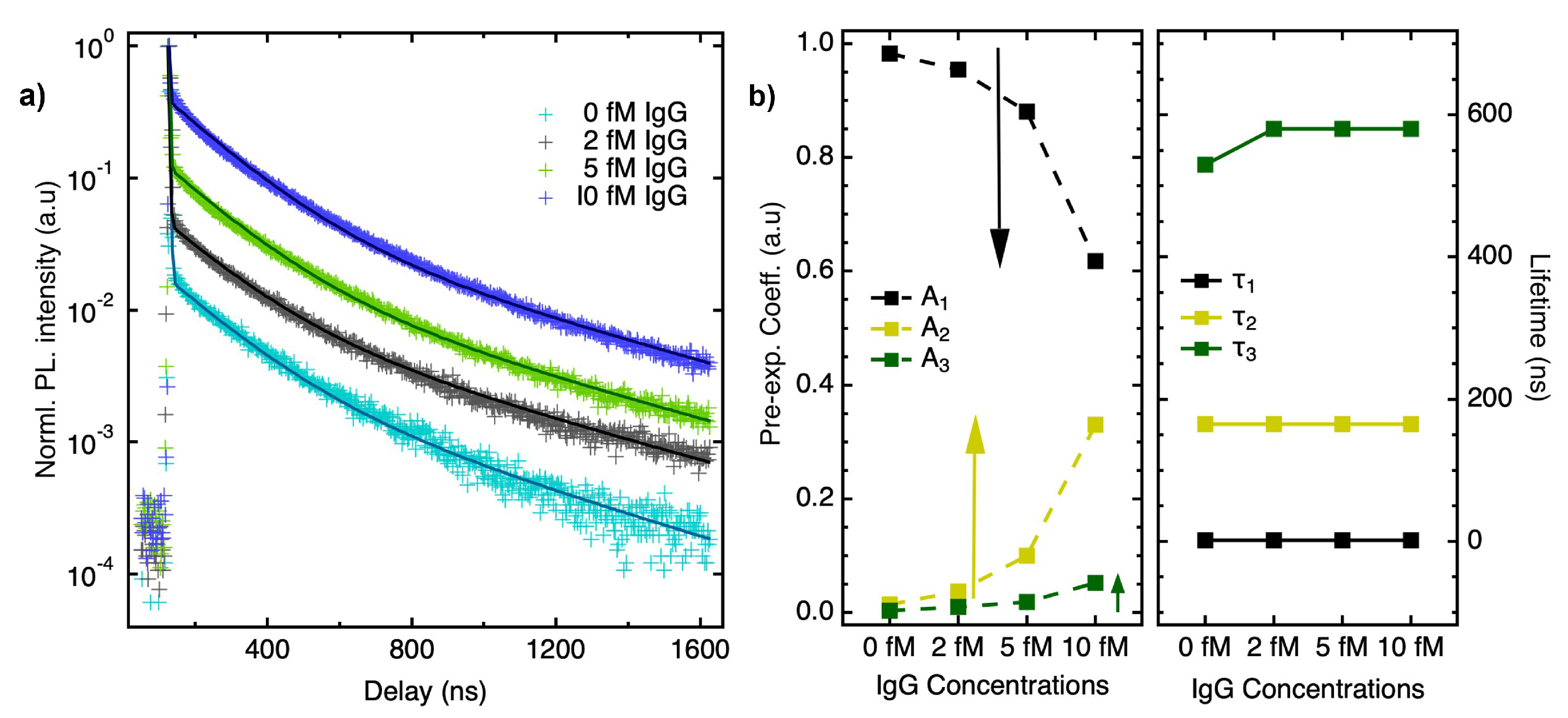
TRPL measurements (Figure 7a) with different concentrations of IgG on anti-IgG functionalized CdSe QDs/SLG further validated the lack of changes in decay times with increasing concentrations of IgG. As shown in Figure 7b, the amplitudes of the second and third exponential decay processes corresponding to and , which are primarily dominant in SLG quenching (cf. Equation 2), were found to increase concomitantly with increasing IgG concentration while the decay times mostly remained unchanged. Based on this observation, it may be asserted that the binding of IgG to anti-IgG coated QDs disrupts the charge redistribution at the QD/SLG interface resulting in an increase in the emissive QD population rather than alterations in the distance between QDs and SLG.
4. Conclusions
This study provides a comprehensive investigation of PL quenching and recovery mechanisms in graphene–QD hybrid systems, with implications for ultrasensitive biosensing applications. Using a combination of SLG-FET measurements, TRPL spectroscopy, and DFT calculations, we demonstrate that charge transfer, rather than Förster-like resonance energy transfer, is the dominant quenching mechanism. The unaltered PL lifetime upon quenching, combined with theoretical charge redistribution analysis, supports a static quenching model governed by rapid electron transfer to graphene prior to optical excitation. Building on these findings, we successfully applied the graphene–QD platform for molecular detection, demonstrating its ability to sense biotin-streptavidin interactions and IgG biomarkers at femtomolar concentrations. The systematic shifts in the Dirac point of the SLG-FET, correlated with PL recovery, provide a robust dual-mode detection strategy that integrates optical and electrical readouts. These results establish a fundamental understanding of charge transfer interactions in graphene-based hybrid nanostructures and open pathways for developing next-generation biosensors with exceptional sensitivity, selectivity, and real-time monitoring capabilities.
Author Contributions
Conceptualization, S.F. and R.P.; methodology, S.F., H.S., and R.P.; formal analysis, S.F. and R.P.; resources, H.S. and R.P.; data curation, S.F and R.P.; writing—original draft preparation, S.F and R.P.; writing—review and editing, H.S. and R.P; visualization, S.F. and R.P.; supervision, H.S. and R.P.; project administration, R.P.; funding acquisition, R.P. All authors have read and agreed to the published version of the manuscript.
Funding
This research was funded by NASA EPSCoR and CORE SC grant numbers 2026213 and 2016773.
Institutional Review Board Statement
Not applicable
Informed Consent Statement
Not applicable
Data Availability Statement
The raw data supporting the conclusions of this article will be made available by the authors on request.
Acknowledgments
R.P. and S.F. thank Clemson Nanomaterials Institute (CNI) for help with Renishaw InVia system to perform continuous wave PL measurements. The authors thank Dr. Prakash Parajuli for his help with quantum espresso in performing DFT calculations.
Conflicts of Interest
The authors declare no conflicts of interest
Abbreviations
The following abbreviations are used in this manuscript:
| QDs | Quantum dots |
| SLG | Single-layer graphene |
| PL | Photoluminescence |
| TRPL | Time-resolved photoluminescence |
| FET | Field-effect transistor |
| RET | Resonance energy transfer |
| DFT | Density functional theory |
| IgG | Immunoglobulin G |
References
- Salihoglu, O.; Kakenov, N.; Balci, O.; et al. Graphene as a Reversible and Spectrally Selective Fluorescence Quencher. Scientific Reports 2016, 6, 33911. [Google Scholar] [CrossRef]
- Meng, L.; Xu, Q.; Zhang, J.; Wang, X. Colloidal quantum dot materials for next-generation near-infrared optoelectronics. Chem. Commun. 2024, 60, 1072–1088. [Google Scholar] [CrossRef]
- Mondal, J.; Lamba, R.; Yukta, Y.; Yadav, R.; Kumar, R.; Pani, B.; Singh, B. Advancements in semiconductor quantum dots: expanding frontiers in optoelectronics, analytical sensing, biomedicine, and catalysis. J. Mater. Chem. C 2024, 12, 10330–10389. [Google Scholar] [CrossRef]
- Liu, C.; Chang, Y.; Norris, T.; et al. Graphene photodetectors with ultra-broadband and high responsivity at room temperature. Nature Nanotechnology 2014, 9, 273–278. [Google Scholar] [CrossRef]
- Abbas, K.; Ji, P.; Ullah, N.; et al. Graphene photodetectors integrated with silicon and perovskite quantum dots. Microsystems & Nanoengineering 2024, 10, 81. [Google Scholar] [CrossRef]
- Geim, A.K. Graphene: Status and Prospects. Science 2009, 324, 1530–1534. [Google Scholar] [CrossRef]
- Geim, A.; Novoselov, K. The rise of graphene. Nature Materials 2007, 6, 183–191. [Google Scholar] [CrossRef]
- Sun, M.; Zhang, C.; Lu, S.; Mahmood, S.; Wang, J.; Sun, C.; Pang, J.; Han, L.; Liu, H. Recent Advances in Graphene Field-Effect Transistor Toward Biological Detection. Advanced Functional Materials 2024, 34, 2405471. [Google Scholar] [CrossRef]
- Zhao, W.; Zhang, W.; Chen, J.; Li, H.; Han, L.; Li, X.; Wang, J.; Song, W.; Xu, C.; Cai, X.; et al. Sensitivity-Enhancing Strategies of Graphene Field-Effect Transistor Biosensors for Biomarker Detection. ACS Sensors 2024, 9, 2705–2727. [Google Scholar] [CrossRef] [PubMed]
- Pourmadadi, M.; Soleimani Dinani, H.; Saeidi Tabar, F.; Khassi, K.; Janfaza, S.; Tasnim, N.; Hoorfar, M. Properties and Applications of Graphene and Its Derivatives in Biosensors for Cancer Detection: A Comprehensive Review. Biosensors 2022, 12. [Google Scholar] [CrossRef]
- Kanai, Y.; Ohmuro-Matsuyama, Y.; Tanioku, M.; Ushiba, S.; Ono, T.; Inoue, K.; Kitaguchi, T.; Kimura, M.; Ueda, H.; Matsumoto, K. Graphene Field Effect Transistor-Based Immunosensor for Ultrasensitive Noncompetitive Detection of Small Antigens. ACS Sensors 2020, 5, 24–28. [Google Scholar] [CrossRef] [PubMed]
- Fu, W.; Jiang, L.; van Geest, E.P.; Lima, L.M.C.; Schneider, G.F. Sensing at the Surface of Graphene Field-Effect Transistors. Advanced Materials 2017, 29, 1603610. [Google Scholar] [CrossRef]
- Federspiel, F.; Froehlicher, G.; Nasilowski, M.; Pedetti, S.; Mahmood, A.; Doudin, B.; Park, S.; Lee, J.O.; Halley, D.; Dubertret, B.; et al. Distance Dependence of the Energy Transfer Rate from a Single Semiconductor Nanostructure to Graphene. Nano Letters 2015, 15, 1252–1258. [Google Scholar] [CrossRef] [PubMed]
- Gaudreau, L.; Tielrooij, K.J.; Prawiroatmodjo, G.E.D.K.; Osmond, J.; de Abajo, F.J.G.; Koppens, F.H.L. Universal Distance-Scaling of Nonradiative Energy Transfer to Graphene. Nano Letters 2013, 13, 2030–2035. [Google Scholar] [CrossRef] [PubMed]
- Prasai, D.; Klots, A.R.; Newaz, A.; Niezgoda, J.S.; Orfield, N.J.; Escobar, C.A.; Wynn, A.; Efimov, A.; Jennings, G.K.; Rosenthal, S.J.; et al. Electrical Control of near-Field Energy Transfer between Quantum Dots and Two-Dimensional Semiconductors. Nano Letters 2015, 15, 4374–4380. [Google Scholar] [CrossRef] [PubMed]
- Kasry, A.; Ardakani, A.A.; Tulevski, G.S.; Menges, B.; Copel, M.; Vyklicky, L. Highly Efficient Fluorescence Quenching with Graphene. The Journal of Physical Chemistry C 2012, 116, 2858–2862. [Google Scholar] [CrossRef]
- Chen, Z.; Berciaud, S.; Nuckolls, C.; Heinz, T.F.; Brus, L.E. Energy Transfer from Individual Semiconductor Nanocrystals to Graphene. ACS Nano 2010, 4, 2964–2968. [Google Scholar] [CrossRef] [PubMed]
- Wen, L.X.; Lv, J.J.; Chen, L.; Li, S.B.; Mou, X.J.; Xu, Y. A fluorescent probe composed of quantum dot labeled aptamer and graphene oxide for the determination of the lipopolysaccharide endotoxin. Mikrochimica Acta 2019, 186, 122. [Google Scholar] [CrossRef]
- Zhang, Y.; Xiao, J.Y.; Zhu, Y.; Tian, L.J.; Wang, W.K.; Zhu, T.T.; Li, W.W.; Yu, H.Q. Fluorescence Sensor Based on Biosynthetic CdSe/CdS Quantum Dots and Liposome Carrier Signal Amplification for Mercury Detection. Analytical Chemistry 2020, 92, 3990–3997. [Google Scholar] [CrossRef]
- Li, M.; Zhou, X.; Guo, S.; Wu, N. Detection of lead (II) with a “turn-on” fluorescent biosensor based on energy transfer from CdSe/ZnS quantum dots to graphene oxide. Biosensors and Bioelectronics 2013, 43, 69–74. [Google Scholar] [CrossRef]
- Sharma, B.; Parajuli, P.; Podila, R. Rapid detection of urokinase plasminogen activator using flexible paper-based graphene-gold platform. Biointerphases 2020, 15, 011004. [Google Scholar] [CrossRef]
- Liu, Z.; Zhou, J.; Wang, X.; Zhao, J.; Zhao, P.; Ma, Y.; Zhang, S.; Huo, D.; Hou, C.; Ren, K. Graphene oxide mediated CdSe quantum dots fluorescent aptasensor for high sensitivity detection of fluoroquinolones. Spectrochimica Acta Part A: Molecular and Biomolecular Spectroscopy 2024, 305, 123497. [Google Scholar] [CrossRef]
- Reznik, I.; Zlatov, A.; Baranov, M.; Zakoldaev, R.; Veniaminov, A.; Moshkalev, S.; Orlova, A. Photophysical Properties of Multilayer Graphene–Quantum Dots Hybrid Structures. Nanomaterials 2020, 10. [Google Scholar] [CrossRef]
- Dong, H.; Gao, W.; Yan, F.; Ji, H.; Ju, H. Fluorescence Resonance Energy Transfer between Quantum Dots and Graphene Oxide for Sensing Biomolecules. Analytical Chemistry 2010, 82, 5511–5517. [Google Scholar] [CrossRef] [PubMed]
- Clapp, A.; Medintz, I.; Mattoussi, H. Förster resonance energy transfer investigations using quantum-dot fluorophores. Chemphyschem 2006, 7, 47–57. [Google Scholar] [CrossRef]
- Raja, A.; Montoya-Castillo, A.; Zultak, J.; Zhang, X.X.; Ye, Z.; Roquelet, C.; Chenet, D.A.; van der Zande, A.M.; Huang, P.; Jockusch, S.; et al. Energy Transfer from Quantum Dots to Graphene and MoS2: The Role of Absorption and Screening in Two-Dimensional Materials. Nano Letters 2016, 16, 2328–2333. [Google Scholar] [CrossRef]
- Neema, P.; Tomy, A.M.; Cyriac, J. Chemical sensor platforms based on fluorescence resonance energy transfer (FRET) and 2D materials. TrAC Trends in Analytical Chemistry 2020, 124, 115797. [Google Scholar] [CrossRef]
- Bharathi, G.; Lin, F.; Liu, L.; Ohulchanskyy, T.Y.; Hu, R.; Qu, J. An all-graphene quantum dot Förster resonance energy transfer (FRET) probe for ratiometric detection of HE4 ovarian cancer biomarker. Colloids and Surfaces B: Biointerfaces 2021, 198, 111458. [Google Scholar] [CrossRef]
- Li, R.; Schneider, L.; Heimbrodt, W.; et al. Gate Tuning of Förster Resonance Energy Transfer in a Graphene - Quantum Dot FET Photo-Detector. Scientific Reports 2016, 6, 28224. [Google Scholar] [CrossRef]
- Xiao, X.; Zhang, Y.; Zhou, L.; Li, B.; Gu, L. Photoluminescence and Fluorescence Quenching of Graphene Oxide: A Review. Nanomaterials (Basel) 2022, 12, 2444. [Google Scholar] [CrossRef]
- Dutta, R.; Kakkar, S.; Mondal, P.; Chauhan, N.; Basu, J.K. Electrical Tuning of Optical Properties of Quantum Dot–Graphene Hybrid Devices: Interplay of Charge and Energy Transfer. The Journal of Physical Chemistry C 2021, 125, 8314–8322. [Google Scholar] [CrossRef]
- Praveena, M.; Mukherjee, A.; Venkatapathi, M.; Basu, J.K. Plasmon-mediated emergence of collective emission and enhanced quantum efficiency in quantum dot films. Phys. Rev. B 2015, 92, 235403. [Google Scholar] [CrossRef]
- Zhu, N.; Zheng, K.; Karki, K.; et al. Sandwiched confinement of quantum dots in graphene matrix for efficient electron transfer and photocurrent production. Scientific Reports 2015, 5, 9860. [Google Scholar] [CrossRef]
- Guo, X.T.; Hua Ni, Z.; Yan Liao, C.; Yan Nan, H.; Zhang, Y.; Wei Zhao, W.; Hui Wang, W. Fluorescence quenching of CdSe quantum dots on graphene. Applied Physics Letters 2013, 103, 201909. [Google Scholar] [CrossRef]
- Sun, Y.; Zhu, H.; Jin, N.; Chen, O.; Zhao, J. Fast lifetime blinking in compact CdSe/CdS core/shell quantum dots. The Journal of Physical Chemistry C 2021, 125, 15433–15440. [Google Scholar]
- Sun, Y.; Wang, Y.; Zhu, H.; Jin, N.; Mohammad, A.; Biyikli, N.; Chen, O.; Chen, K.; Zhao, J. Excitation wavelength-dependent photoluminescence decay of single quantum dots near plasmonic gold nanoparticles. The Journal of Chemical Physics 2022, 156. [Google Scholar]
- Gallagher, S.A.; Moloney, M.P.; Wojdyla, M.; Quinn, S.J.; Kelly, J.M.; Gun’ko, Y.K. Synthesis and spectroscopic studies of chiral CdSe quantum dots. Journal of Materials Chemistry 2010, 20, 8350–8355. [Google Scholar]
- De, C.K.; Routh, T.; Roy, D.; Mandal, S.; Mandal, P.K. Highly photoluminescent InP based core alloy shell QDs from air-stable precursors: excitation wavelength dependent photoluminescence quantum yield, photoluminescence decay dynamics, and single particle blinking dynamics. The Journal of Physical Chemistry C 2018, 122, 964–973. [Google Scholar] [CrossRef]
- Béraud, A.; Sauvage, M.; Bazán, C.M.; Tie, M.; Bencherif, A.; Bouilly, D. Graphene field-effect transistors as bioanalytical sensors: design, operation and performance. Analyst 2021, 146, 403–428. [Google Scholar] [CrossRef]
- Lin, W.; Tian, B.; Zhuang, P.; Yin, J.; Zhang, C.; Li, Q.; Shih, T.m.; Cai, W. Graphene-Based Fluorescence-Quenching-Related Fermi Level Elevation and Electron-Concentration Surge. Nano Letters 2016, 16, 5737–5741. [Google Scholar] [CrossRef] [PubMed]
- Fu, W.; Jiang, L.; van Geest, E.P.; Lima, L.M.C.; Schneider, G.F. Sensing at the Surface of Graphene Field-Effect Transistors. Advanced Materials 2017, 29, 1603610. [Google Scholar] [CrossRef] [PubMed]
- Vidarsson, G.; Dekkers, G.; Rispens, T. IgG subclasses and allotypes: from structure to effector functions. Frontiers in Immunology 2014, 5, 520. [Google Scholar] [CrossRef] [PubMed]
Figure 1.
a) A schematic representation of the SLG-FET device and the measurement scheme showing both optical and electrical detection. While a 532 nm incident laser excites the QDs for optical detection, transfer characteristics are simultaneously measured using the FET channels, b) Raman spectrum of the chemical vapor deposition grown pristine SLG sample obtained under 532 nm excitation shows a 2D band that is more intense than the graphitic or G band consistent with SLG. The solid-line shows the fit to the experimental spectrum. AFM images of the graphene sample (c) before and (d) after CdSe QD deposition show the increase in average surface roughness from 90 pm to 120 nm.
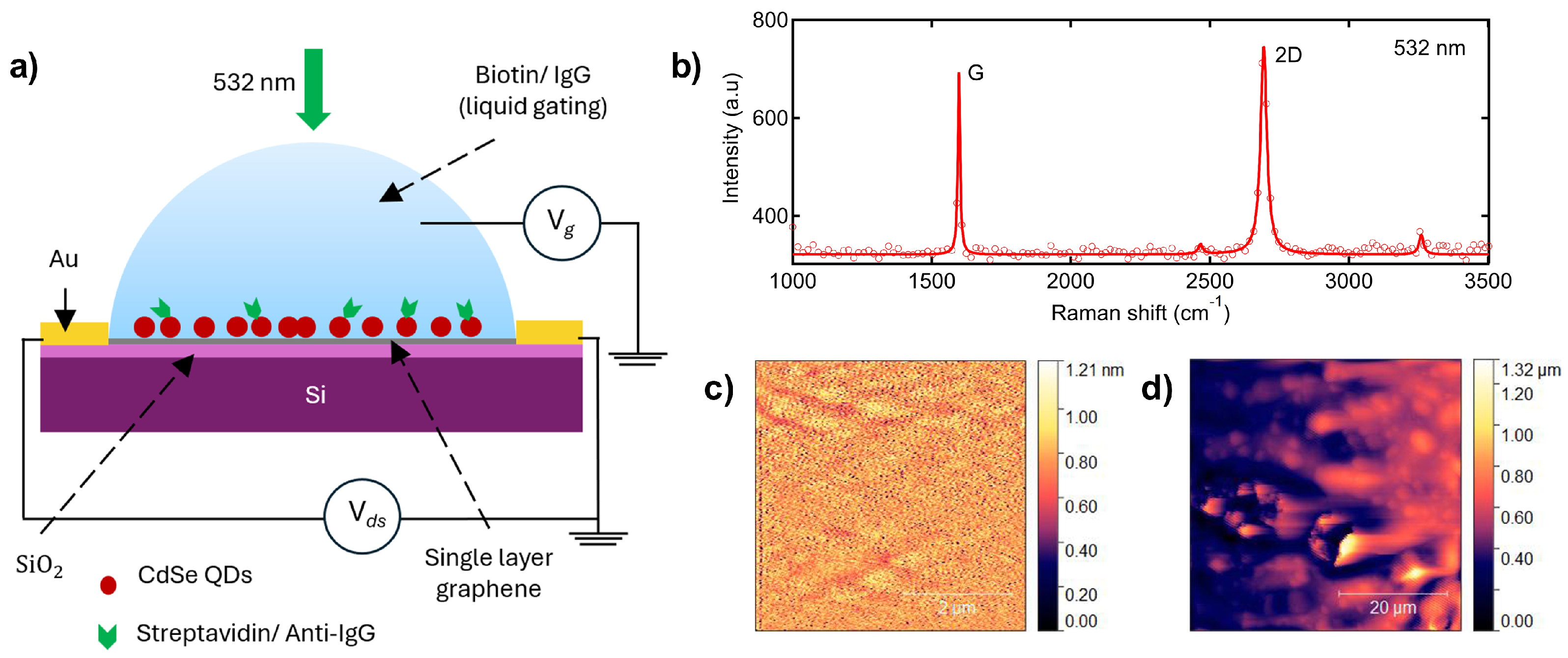
Figure 2.
a) PL emission spectra obtained from 10 nM QDs dropcasted on Si/SiO2 and SLG coated Si/SiO2 substrates. All data was averaged over at least three measurements. The background PL emission from bare Si/SiO2 is also shown (green line). A magnified view of the quenched emission is shown in the inset. The quenching of CdSe QD PL on SLG surface is clearly seen from the fluorescence microscopy images of QDs on Si/SiO2 and SLG coated Si/SiO2 substrates (b-c).
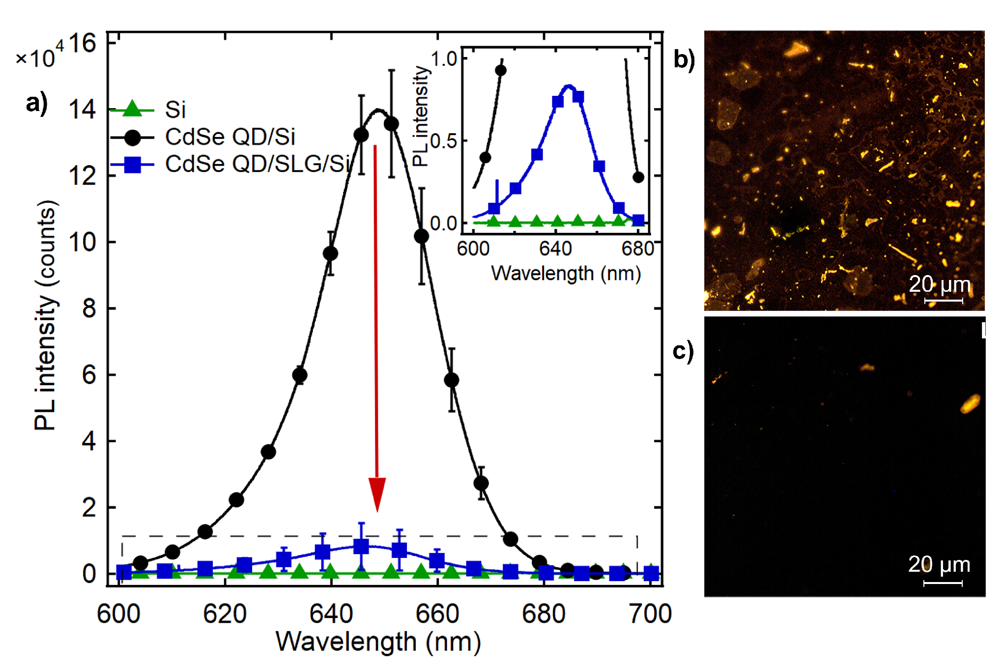
Figure 3.
a) Normalized TRPL traces of a) CdSe QDs deposited on bare quartz and SLG-quartz substrates. Solid lines are obtained through triexponential fits. The fit parameters are shown in the inset. Measurements were taken drop casting 5 µl of 10 nM QDs onto the substrate, followed by overnight ambient drying. (b-c) Three-dimensional images of CdSe/SLG hybrids from Quantum Espresso with charge depletion (/accumulation) shown in blue (/red) color, and d) Charge transfer profile along the z-axis. The total amount of charge transfer between the graphene and the CdSe layer was calculated by integrating the shaded area.
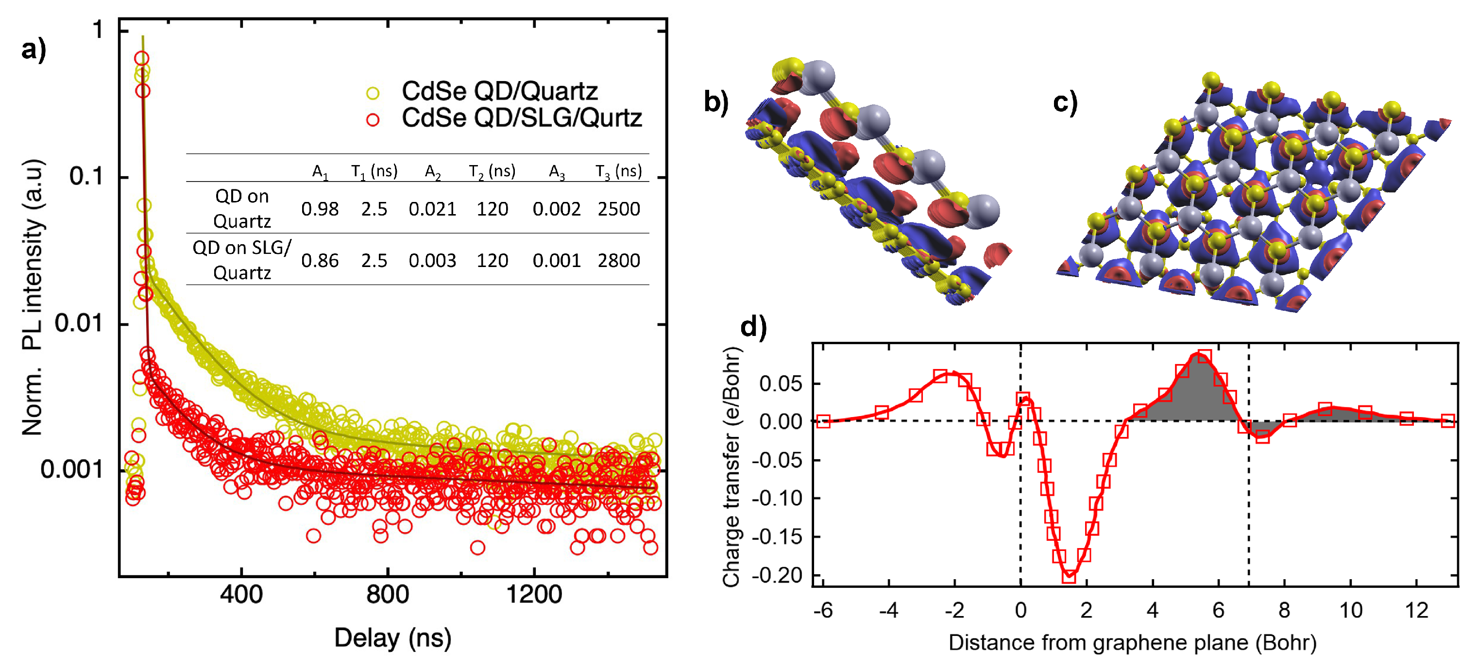
Figure 4.
a) Typical transfer curves showing of our SLG-FET before and after CdSe QD deposition. The deposition was carried out by dropcasting 5 µl of 10 nM QD in the standard buffer. The inset at the bottom displays typical ambipolar transfer characteristics showing that the type of carriers in graphene can continuously be modulated from holes (left branch) to electrons (right branch) by varying the gate voltage . The charge-neutrality point (CNP) is located at the transition between the electron and hole regime, where the current is minimum. A schematic illustration of the shift in the Fermi level across graphene’s Dirac cone upon n and p-type doping is shown in the top inset. b) Optical microscopy and c) AFM images of the SLG-FET device showing graphene channels with common drain and individual sources. Contacts were made using non-encapsulated Au gate channel enabling liquid gating. Fluorescence microscopy images before (d) and after (e) QD deposition show strong QD luminescence everywhere except on the SLG area within the circular area (middle dark region).
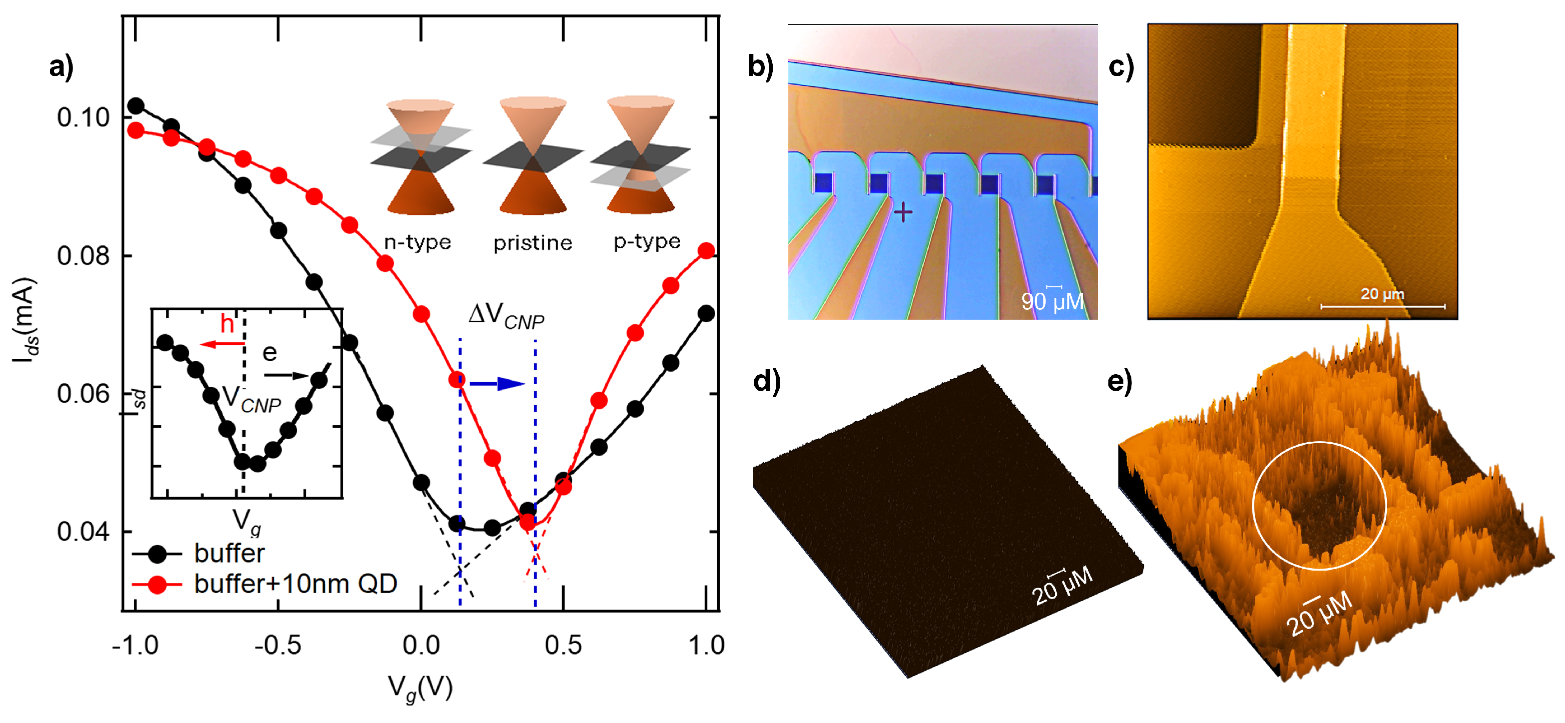
Figure 5.
a) PL Emission from streptavidin-conjugated CdSe QDs deposited on SLG increased with the addition of biotin. PL measurements were performed in triplicates for each biotin concentration. The inset shows the maximum PL intensity as a function of biotin concentration. (b-d) A lateral shift in the transfer characteristics (VCNP) was observed upon the addition of biotin to streptavidin QDs on SLG-FET. All the FET measurements were also performed in triplicates on three different SLG-FET channels shown in (b-d). Sample deposition was carried out by drop casting 4 µl of biotin samples prepared in the standard buffer. The shift in (e) and (f) Ids at VCNP as a function of biotin concentration ranging from 0.5-160 fM with buffer solution as the background control. A saturation of the sample sensitivity is observed for concentrations above 20 fM.
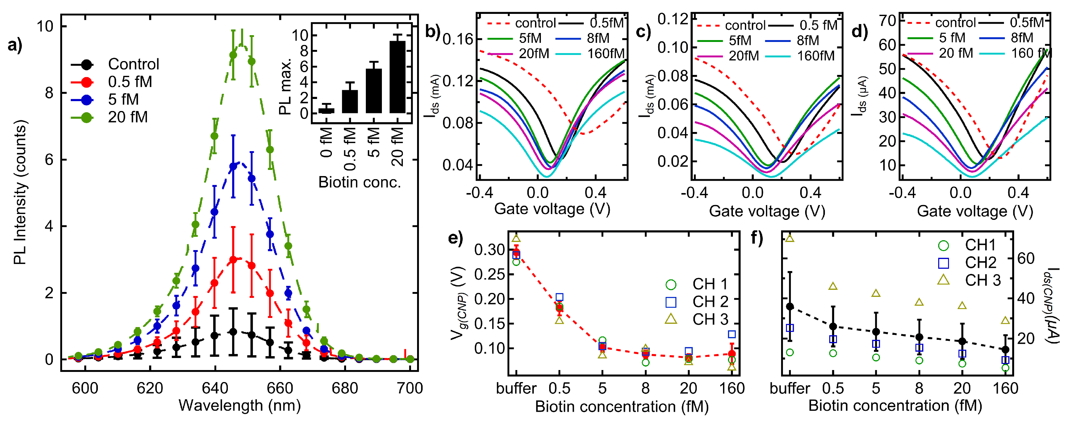
Figure 6.
Sensing characteristics of our SLG-FET device functionalized with anti-IgG antibody-coated CdSe QDs for sensing IgG (0.5-25 fM). (a) PL emission at different IgG concentrations. All measurements were performed in triplicates. The inset shows the maximum PL as a function of IgG concentrations, (b-e) Electrical characteristics were measured similar to biotin. In contrast to biotin, IgG exhibits a positive shift due to p-type doping. All measurements were performed on at least three different SLG channels, (f) Real-time monitoring of Ids demonstrates the ability of SLG-FET to rapidly detect changes on SLG surface upon antigen-antibody binding, highlighting its potential as a robust biosensor.
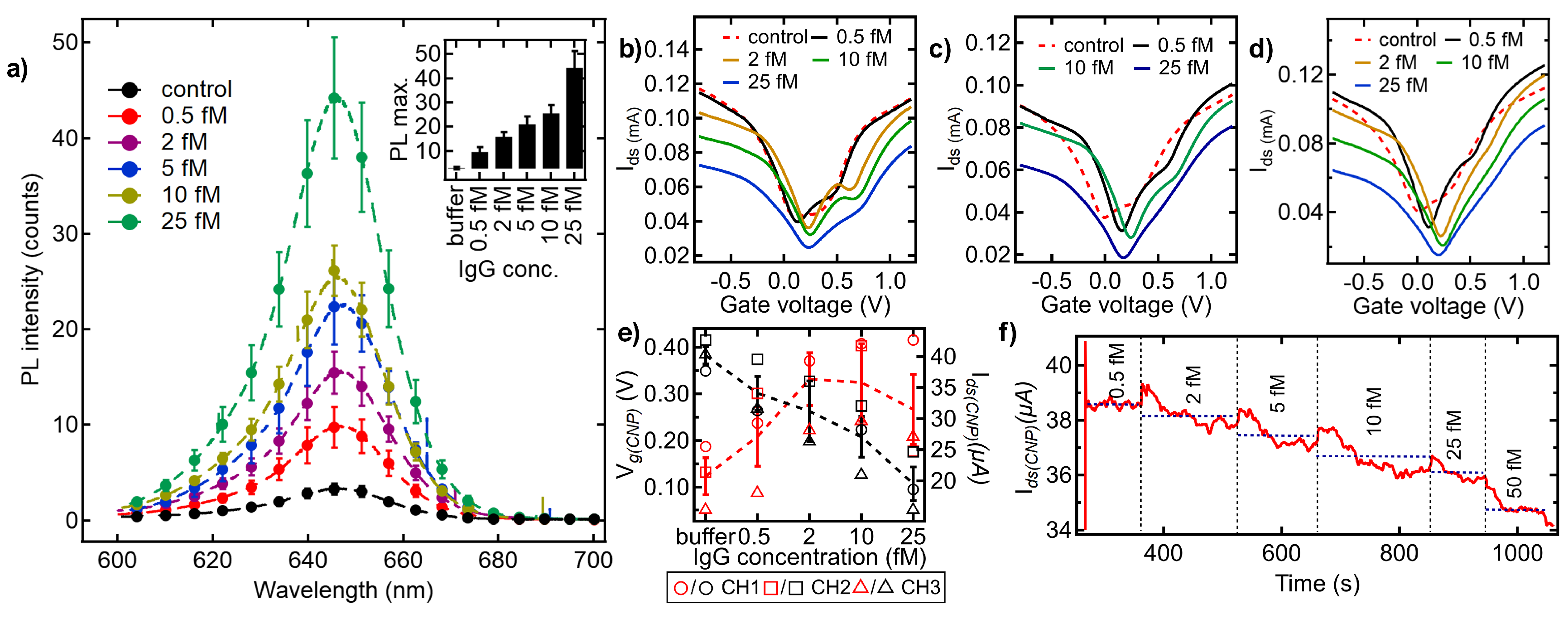
Figure 7.
TRPL traces for different IgG concentrations (0- 10 fM ) added to anti-IgG conjugated CdSe/SLG/Quartz surface. The data was fitted to tri-exponential, which are shown as solid lines. b) A detailed comparison of all pre-exponential amplitudes and decay times obtained from the fits.
Figure 7.
TRPL traces for different IgG concentrations (0- 10 fM ) added to anti-IgG conjugated CdSe/SLG/Quartz surface. The data was fitted to tri-exponential, which are shown as solid lines. b) A detailed comparison of all pre-exponential amplitudes and decay times obtained from the fits.
Disclaimer/Publisher’s Note: The statements, opinions and data contained in all publications are solely those of the individual author(s) and contributor(s) and not of MDPI and/or the editor(s). MDPI and/or the editor(s) disclaim responsibility for any injury to people or property resulting from any ideas, methods, instructions or products referred to in the content. |
© 2025 by the authors. Licensee MDPI, Basel, Switzerland. This article is an open access article distributed under the terms and conditions of the Creative Commons Attribution (CC BY) license (http://creativecommons.org/licenses/by/4.0/).
Copyright: This open access article is published under a Creative Commons CC BY 4.0 license, which permit the free download, distribution, and reuse, provided that the author and preprint are cited in any reuse.


